Äîêóìåíòàöèÿ è îïèñàíèÿ www.docs.chipfind.ru
Philips
Semiconductors
74LVC2952A
Octal registered tranceiver with 5-volt
tolerant inputs/ouputs (3-State)
Product specification
1998 Jul 29
INTEGRATED CIRCUITS
Philips Semiconductors
Product specification
74LVC2952A
Octal registered tranceiver with 5-volt tolerant
inputs/ouputs (3-State)
2
1998 Jul 29
853-1993 19803
FEATURES
·
5-volt tolerant inputs/outputs, for interfacing with 5-volt logic
·
Wide supply voltage range of 1.2 V to 3.6 V
·
In accordance with the JEDEC standard no. 8-1 A
·
Inputs accept voltages up to 5.5 V
·
CMOS low power consumption
·
Flow-through pin-out architecture
·
3-State outputs
·
Direct interface with TTL levels
·
Integrated 30
W
damping resistor
DESCRIPTION
The 74LVC2952A is a low-power, low-voltage, Si-gate CMOS device
and superior to most advanced CMOS compatible TTL families. The
74LVC2952A is an octal non-inverting registered transceiver. Two 8-bit
back to back registers store data flowing in both directions between two
bidirectional busses. Data applied to the inputs is entered and stored on
the rising edge of the clock (CPnn) provided that the clock enable CE
nn
)
is LOW. The data is then present at the 3-State output buffers, but is
only accessible when the output enable input (OE
nn
) is LOW. Data flow
from A inputs to B outputs is the same as for B inputs to A outputs. The
74LVC2952A is identical to the 74LVC2953A but has non-inverting
outputs.
QUICK REFERENCE DATA
GND = 0 V; T
amb
= 25
°
C; t
r
=t
f
2.5 ns
SYMBOL
PARAMETER
CONDITIONS
TYPICAL
UNIT
t
PHL
/t
PLH
Propagation delay
CP
nn
to A
n
, B
n
C
L
= 50 pF;
V
CC
= 3.3 V
4.3
ns
f
max
Maximum clock frequency
150
MHz
C
I
Input capacitance
5
pF
C
I/O
Input/output capacitance
10
pF
C
PD
Power dissipation capacitance per buffer
V
CC
= 3.3V
1
31
pF
NOTE:
1
C
PD
is used to determine the dynamic power dissipation (P
D
in
µ
W)
P
D
= C
PD
×
V
CC
2
×
f
i
)
(C
L
×
V
CC
2
×
f
o
) where:
f
i
= input frequency in MHz; C
L
= output load capacity in pF;
f
o
= output frequency in MHz; V
CC
= supply voltage in V;
(C
L
×
V
CC
2
×
f
o
) = sum of the outputs.
ORDERING INFORMATION
PACKAGES
TEMPERATURE RANGE
OUTSIDE NORTH AMERICA
NORTH AMERICA
PKG. DWG. #
24-Pin Plastic SO
40
°
C to +125
°
C
74LVC2952A D
74LVC2952A D
SOT137-1
24-Pin Plastic SSOP Type II
40
°
C to +125
°
C
74LVC2952A DB
74LVC2952A DB
SOT340-1
24-Pin Plastic TSSOP Type I
40
°
C to +125
°
C
74LVC2952A PW
74LVC2952APW DH
SOT355-1
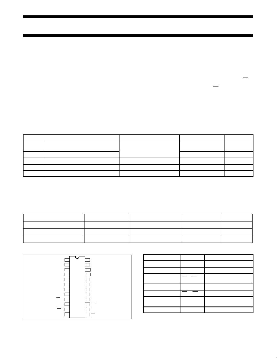
PIN CONFIGURATION
SV01716
B
7
B
6
B
5
B
4
B
3
B
2
B
1
B
0
OE
AB
CP
AB
CE
AB
CE
BA
CP
BA
OE
BA
1
2
3
4
5
6
7
8
9
10
11
12
GND
V
CC
A
7
A
6
A
5
A
4
A
3
A
2
A
1
A
0
24
23
22
21
20
19
18
17
16
15
14
13
PIN DESCRIPTION
PIN NUMBER
SYMBOL
FUNCTION
8, 7, 6, 5, 4, 3, 2, 1,
B
0
to B
7
B data inputs/outputs
12
GND
Ground (0 V)
9, 15
OE
AB
,OE
BA
Output enable inputs
(active LOW)
10, 14
CP
AB
, CP
BA
Clock inputs
11, 13,
CE
AB
, CE
BA
Clock enable inputs
16, 17, 18, 19, 20,
21, 22, 23
A
0
to A
7
A data inputs/outputs
24
V
CC
Positive supply voltage
Philips Semiconductors
Product specification
74LVC2952A
Octal registered tranceiver with 5-volt tolerant
inputs/ouputs (3-State)
1998 Jul 29
3
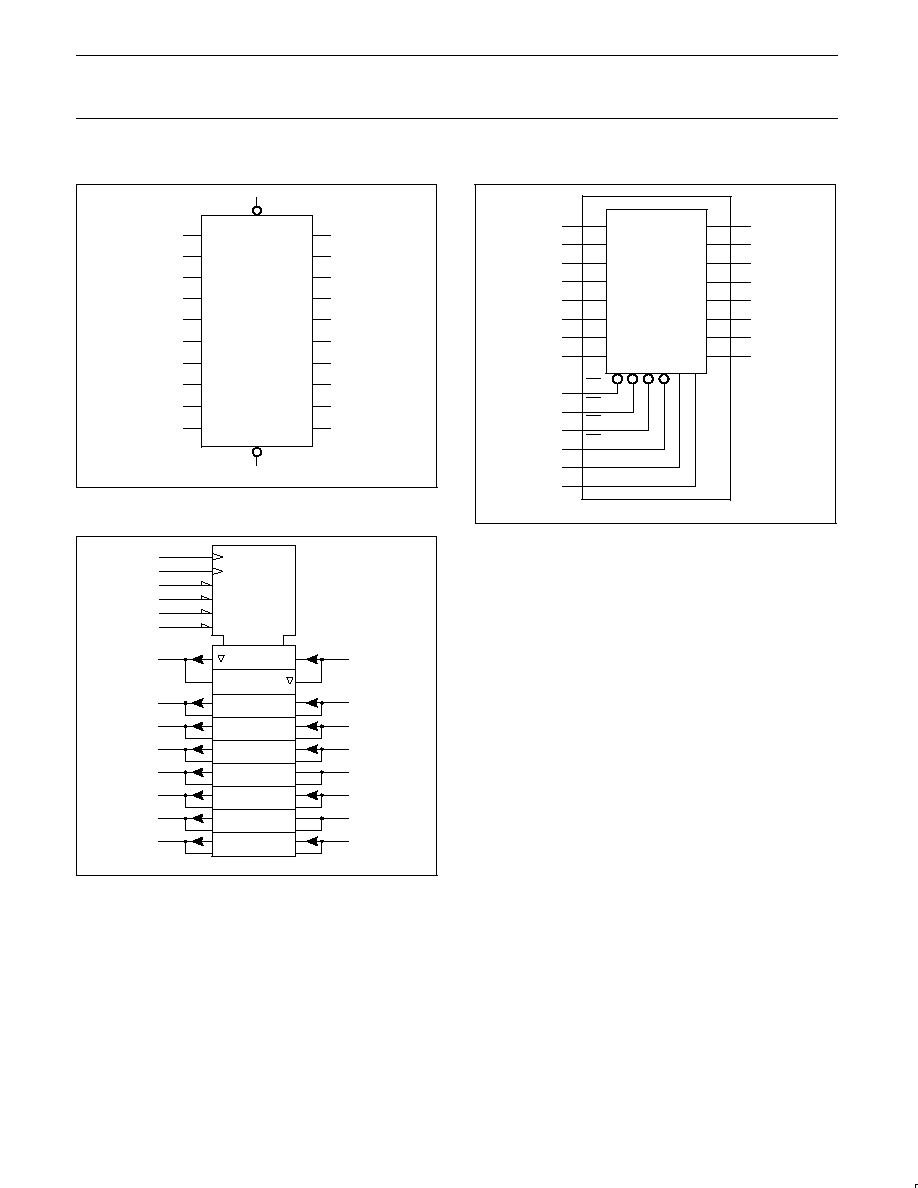
LOGIC SYMBOL (IEEE/IEC)
SV01717
15
16
17
18
19
20
21
22
23
10
11
CP AB
CE AB
A 0
A 1
A 2
A 3
A 4
A 5
A 6
A 7
OE AB
OE BA
9
B 0
B 1
B 2
B 3
B 4
B 5
B 6
B 7
CP BA
CE BA
14
13
8
7
6
5
4
3
2
1
LOGIC SYMBOL
SV01718
3
4
5D
6D
16
17
18
19
20
21
22
23
8
7
6
5
4
3
2
1
1
1
G1
13
G2
11
2 C6
1 C5
10
14
EN4
EN3
15
9
FUNCTIONAL DIAGRAM
SV01719
B 0
8
16
A 0
B 1
7
17
A 1
B 2
6
18
A 2
B 3
5
19
A 3
B 4
4
20
A 4
B 5
3
21
A 5
OE AB
OE BA
CE AB
CE BA
CP AB
CP BA
B 6
2
22
A 6
B 7
1
23
A 7
14
10
13
11
15
9
Philips Semiconductors
Product specification
74LVC2952A
Octal registered tranceiver with 5-volt tolerant
inputs/ouputs (3-State)
1998 Jul 29
4
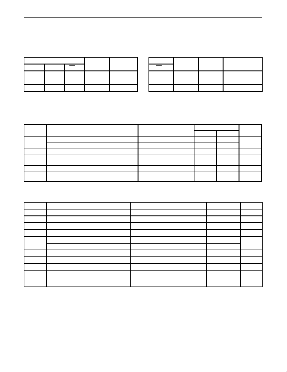
FUNCTION TABLE for register A
n
or B
n
INPUTS
INTERNAL
OPERATING
A
n
or B
n
CP
nn
CE
nn
Q
MODE
X
X
H
NC
Hold data
L
L
L
Load data
H
L
H
Load data
NOTES:
H
=
HIGH voltage level
L
=
LOW voltage level
X
=
don't care
FUNCTION TABLE for output enable
INPUTS
INTERNAL
A
n
or B
n
OPERATING MODE
OE
nn
Q
n
n
OUTPUTS
OPERATING MODE
H
X
Z
Disable outputs
L
L
L
Enable outputs
L
H
H
Enable outputs
Z
=
high impedance OFF-state
=
Low-to-High transition
NC =
no change
RECOMMENDED OPERATING CONDITIONS
SYMBOL
PARAMETER
CONDITIONS
LIMITS
UNIT
SYMBOL
PARAMETER
CONDITIONS
MIN
MAX
UNIT
V
CC
DC supply voltage (for max. speed performance)
2.7
3.6
V
V
CC
DC supply voltage (for low-voltage applications)
1.2
3.6
V
V
I
DC input voltage range
0
5.5
V
V
I/O
DC output voltage range; output HIGH or LOW state
0
V
CC
V
V
I/O
DC input voltage range; output 3-State
0
5.5
V
T
amb
Operating free-air temperature range
40
+85
°
C
t
r
, t
f
Input rise and fall times
V
CC
= 1.2 to 2.7V
V
CC
= 2.7 to 3.6V
0
0
20
10
ns/V
ABSOLUTE MAXIMUM RATINGS
1
In accordance with the Absolute Maximum Rating System (IEC 134).
Voltages are referenced to GND (ground = 0 V).
SYMBOL
PARAMETER
CONDITIONS
RATING
UNIT
V
CC
DC supply voltage
0.5 to +6.5
V
I
IK
DC input diode current
V
I
t
0
50
mA
V
I
DC input voltage
Note 2
0.5 to +6.5
V
I
OK
DC output diode current
V
O
u
V
CC
or V
O
t
0
"
50
mA
V
I/O
DC output voltage; output HIGH or LOW
Note 2
0.5 to V
CC
+0.5
V
V
I/O
DC output voltage; output 3-State
Note 2
0.5 to 6.5
V
I
O
DC output source or sink current
V
O
= 0 to V
CC
"
50
mA
I
GND
, I
CC
DC V
CC
or GND current
"
100
mA
T
stg
Storage temperature range
65 to +150
°
C
Power dissipation per package
P
TOT
plastic mini-pack (SO)
above +70
°
C derate linearly with 8 mW/K
500
mW
plastic shrink mini-pack (SSOP and TSSOP)
above +60
°
C derate linearly with 5.5 mW/K
500
mW
NOTES:
1
Stresses beyond those listed may cause permanent damage to the device. These are stress ratings only and functional operation of the
device at these or any other conditions beyond those indicated under "recommended operating conditions" is not implied. Exposure to
absolute-maximum-rated conditions for extended periods may affect device reliability.
2
The input and output voltage ratings may be exceeded if the input and output current ratings are observed.
Philips Semiconductors
Product specification
74LVC2952A
Octal registered tranceiver with 5-volt tolerant
inputs/ouputs (3-State)
1998 Jul 29
5
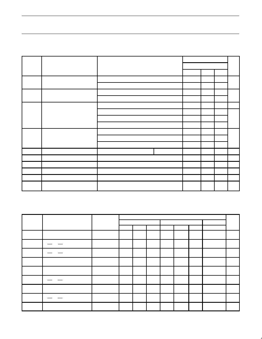
DC ELECTRICAL CHARACTERISTICS
Over recommended operating conditions voltages are referenced to GND (ground = 0V)
LIMITS
SYMBOL
PARAMETER
TEST CONDITIONS
Temp = -40
°
C to +85
°
C
UNIT
MIN
TYP
1
MAX
V
HIGH level Input voltage
V
CC
= 1.2V
V
CC
V
V
IH
HIGH level Input voltage
V
CC
= 2.7 to 3.6V
2.0
V
V
LOW level Input voltage
V
CC
= 1.2V
GND
V
V
IL
LOW level Input voltage
V
CC
= 2.7 to 3.6V
0.8
V
V
CC
= 2.7V; V
I
= V
IH
or V
IL
; I
O
= 12mA
V
CC
*
0.5
V
V
CC
= 3 0V; V = V
or V ; I
O
= 100
µ
A
V
CC
0 2
V
CC
V
O
HIGH level output voltage
V
CC
= 3.0V; V
I
= V
IH
or V
IL
; I
O
= 100
µ
A
V
CC
*
0.2
V
CC
V
OH
HIGH level output voltage
V
CC
= 3.0V; V
I
= V
IH
or V
IL;
I
O
= 18mA
V
CC
*
0.6
V
V
CC
= 3.0V; V
I
= V
IH
or V
IL;
I
O
= 24mA
V
CC
*
0.8
V
CC
= 2.7V; V
I
= V
IH
or V
IL
; I
O
= 12mA
0.40
V
OL
LOW level output voltage
V
CC
= 3.0V; V
I
= V
IH
or V
IL
; I
O
= 100
µ
A
0.20
V
V
CC
= 3.0V; V
I
= V
IH
or V
IL;
I
O
= 24mA
0.55
I
I
Input leakage current
V
CC
= 3.6V; V
I
= 5.5V or GND
Not for I/O pins
"
0.1
"
5
µ
A
I
IHZ
/I
ILZ
Input current for common I/O pins
V
CC
= 3.6V; V
I
= 5.5V or GND
"
0.1
"
15
µ
A
I
OZ
3-State output OFF-state current
V
CC
= 3.6V; V
I
= V
IH
or V
IL
; V
O
= 5.5V or GND
0.1
"
5
µ
A
I
off
Power off leakage supply
V
CC
= 0.0V; V
I
or V
O
= 5.5V
"
10
µ
A
I
CC
Quiescent supply current
V
CC
= 3.6V; V
I
= V
CC
or GND; I
O
= 0
0.1
10
µ
A
I
CC
Additional quiescent supply
current per input pin
V
CC
= 2.7V to 3.6V; V
I
= V
CC
0.6V; I
O
= 0
5
500
µ
A
NOTES:
1
All typical values are at V
CC
= 3.3V and T
amb
= 25
°
C.
AC CHARACTERISTICS
GND = 0 V; t
r
= t
f
v
2.5 ns; C
L
= 50 pF; R
L
= 500
W
LIMITS
SYMBOL
PARAMETER
WAVEFORM
V
CC
= 3.3V
±
0.3V
V
CC
= 2.7V
V
CC
= 1.2V
UNIT
MIN
TYP
MAX
MIN
TYP
MAX
TYP
t
PHL
/t
PLH
Propagation delay
CP
BA
, CP
AB
to A
n
, B
n
Figures 1, 4
1.5
4.1
7.6
1.5
4.4
8.6
16
ns
t
PZH/
t
PZL
3-state output enable time
OE
BA
, OE
AB
, to A
n
, B
n
Figures 3, 4
1.5
3.9
7.6
1.5
4.7
8.6
16
ns
t
PHZ/
t
PLZ
3-state output disable time
OE
BA
, OE
AB
, to A
n
, B
n
Figures 3, 4
1.5
3.4
6.6
1.5
3.8
7.6
8
ns
t
w
CP
AB
, CP
BA
pulse width,
HIGH or LOW
Figure 1
3.0
1.5
3.0
1.5
ns
t
su
Set-up time HIGH or LOW
A
n
, B
n
to CP
AB
, CP
BA
Figure 2
2.0
0.5
2.0
ns
t
su
Set-up time, HIGH or LOW
CE
AB
, CE
BA
to CP
AB
, CP
BA
Figure 2
2.0
0.5
2.0
ns
t
h
Hold time
A
n
, B
n
to CP
AB
, CP
BA
Figure 2
1.5
0.6
1.5
ns
t
h
Hold time
CE
AB
, CE
BA
to CP
AB
, CP
BA
Figure 2
1.5
0
1.5
ns
f
max
Maximum clock pulse
frequency
Figure 2
100
150
80
MHz
NOTE:
These typical values are at V
CC
= 3.3V and T
amb
= 25
°
C.
Philips Semiconductors
Product specification
74LVC2952A
Octal registered tranceiver with 5-volt tolerant
inputs/ouputs (3-State)
1998 Jul 29
6
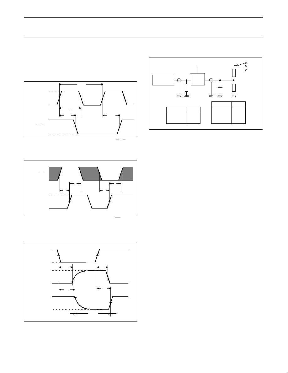
AC WAVEFORMS
V
M
= 0.6 V at V
CC
=
1.2 V
V
M
= 1.0 V at V
CC
=
2.0 V
V
M
= 1.5 V at V
CC
=
3.0 V
V
OL
and V
OH
are the typical output voltage drop that occur with the
3-State output load.
SV01720
GND
V
OL
V
I
V
OH
A
n
, B
n
OUTPUT
V
M
CP
XX
INPUT
V
M
t
PLH
t
PHL
1/f
max
t
W
Figure 1. Clock input (CP
BA
, CP
AB
) to output (B
n
, A
n
)
propagation delays, the clock pulse width
and the maximum clock frequency.
SV01721
V
M
A
n
, B
n
, CE
nn
INPUT
CP
XX
INPUT
V
M
t
su
t
su
t
h
t
h
GND
GND
V
I
V
I
Figure 2. Set-up and hold times for the A
n
, B
n
and CE
nn
inputs.
NOTE:
The shaded areas indicate when the input is permitted to
change for predictable output performance
SV01722
GND
V
I
V
CC
V
X
V
Y
outputs
disabled
outputs
enabled
outputs
enabled
t
PHZ
t
PZH
t
PZL
t
PLZ
V
OL
V
OH
GND
V
M
V
M
V
M
CP
XX
INPUT
OUTPUT
LOWtoOFF
OFFtoLOW
OUTPUT
HIGH-to-OFF
OFF-to-HIGH
Figure 3. 3-State enable and disable times.
TEST CIRCUIT
PULSE
GENERATOR
V
I
R
T
D.U.T.
V
O
C
L
50pF
S
1
2 x V
CC
Open
GND
500
500
V
CC
V
I
t
2.7V
V
CC
2.7V 3.6V
2.7V
Test
S
1
GND
t
PLZ
/t
PZL
2 x V
CC
t
PHZ
/t
PZH
t
PLH
/t
PHL
Open
SY00003
V
CC
Figure 4. Load circuitry for switching times.
Philips Semiconductors
Product specification
74LVC2952A
Octal registered tranceiver with 5-volt tolerant
inputs/ouputs (3-State)
1998 Jul 29
7
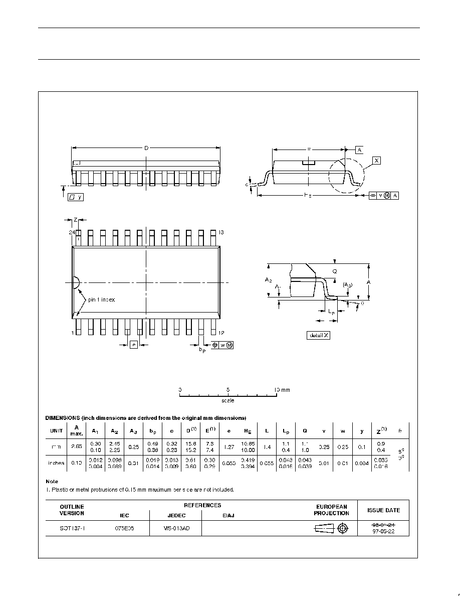
SO24:
plastic small outline package; 24 leads; body width 7.5 mm
SOT137-1
Philips Semiconductors
Product specification
74LVC2952A
Octal registered tranceiver with 5-volt tolerant
inputs/ouputs (3-State)
1998 Jul 29
8
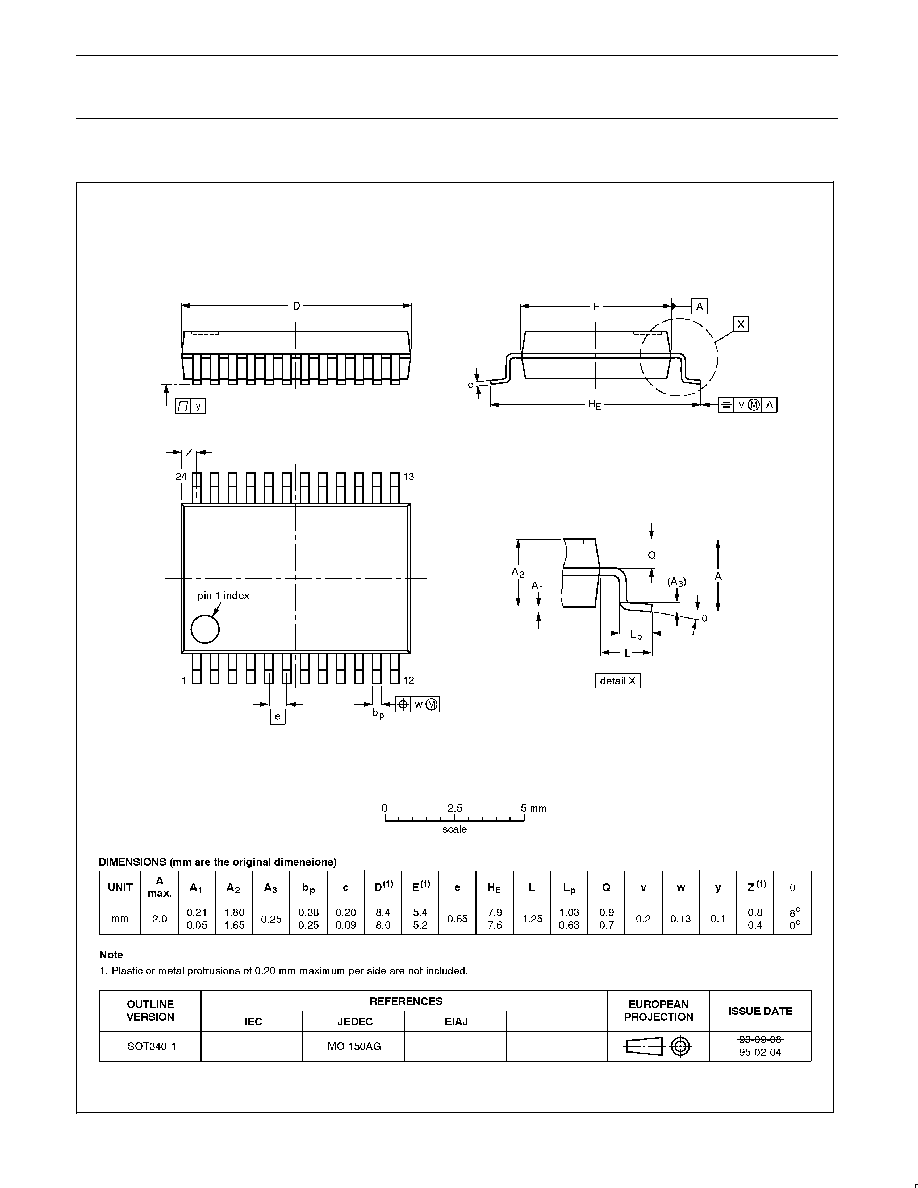
SSOP24:
plastic shrink small outline package; 24 leads; body width 5.3 mm
SOT340-1
Philips Semiconductors
Product specification
74LVC2952A
Octal registered tranceiver with 5-volt tolerant
inputs/ouputs (3-State)
1998 Jul 29
9
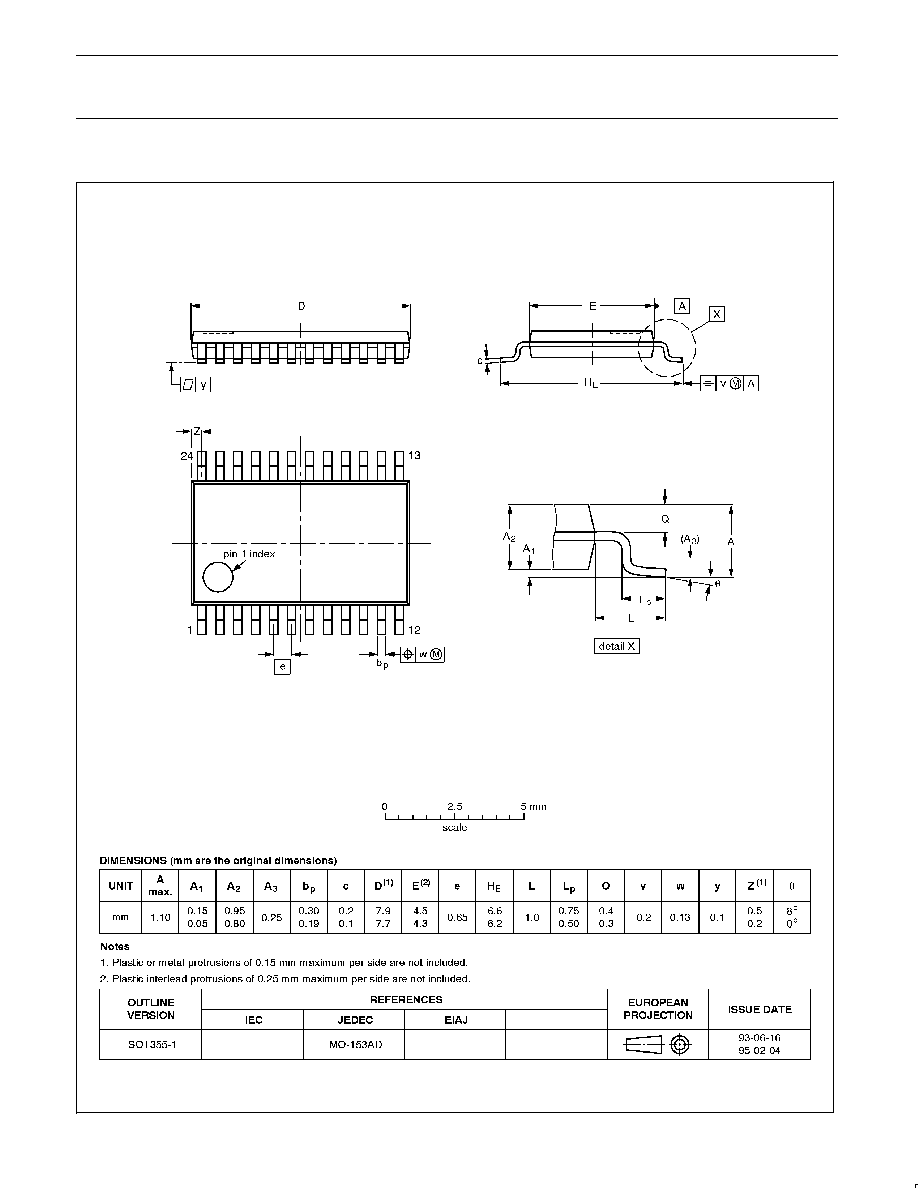
TSSOP24:
plastic thin shrink small outline package; 24 leads; body width 4.4 mm
SOT355-1

Philips Semiconductors
Product specification
74LVC2952A
Octal registered tranceiver with 5-volt tolerant
inputs/ouputs (3-State)
1998 Jul 29
10
NOTES
Philips Semiconductors
Product specification
74LVC2952A
Octal registered tranceiver with 5-volt tolerant
inputs/ouputs (3-State)
yyyy mmm dd
11
Definitions
Short-form specification -- The data in a short-form specification is extracted from a full data sheet with the same type number and title. For
detailed information see the relevant data sheet or data handbook.
Limiting values definition -- Limiting values given are in accordance with the Absolute Maximum Rating System (IEC 134). Stress above one
or more of the limiting values may cause permanent damage to the device. These are stress ratings only and operation of the device at these or
at any other conditions above those given in the Characteristics sections of the specification is not implied. Exposure to limiting values for extended
periods may affect device reliability.
Application information -- Applications that are described herein for any of these products are for illustrative purposes only. Philips
Semiconductors make no representation or warranty that such applications will be suitable for the specified use without further testing or
modification.
Disclaimers
Life support -- These products are not designed for use in life support appliances, devices or systems where malfunction of these products can
reasonably be expected to result in personal injury. Philips Semiconductors customers using or selling these products for use in such applications
do so at their own risk and agree to fully indemnify Philips Semiconductors for any damages resulting from such application.
Right to make changes -- Philips Semiconductors reserves the right to make changes, without notice, in the products, including circuits, standard
cells, and/or software, described or contained herein in order to improve design and/or performance. Philips Semiconductors assumes no
responsibility or liability for the use of any of these products, conveys no license or title under any patent, copyright, or mask work right to these
products, and makes no representations or warranties that these products are free from patent, copyright, or mask work right infringement, unless
otherwise specified.
Philips Semiconductors
811 East Arques Avenue
P.O. Box 3409
Sunnyvale, California 940883409
Telephone 800-234-7381
©
Copyright Philips Electronics North America Corporation 1998
All rights reserved. Printed in U.S.A.
print code
Date of release: 08-98
Document order number:
9397-750-04524
Philips
Semiconductors
Data sheet
status
Objective
specification
Preliminary
specification
Product
specification
Product
status
Development
Qualification
Production
Definition
[1]
This data sheet contains the design target or goal specifications for product development.
Specification may change in any manner without notice.
This data sheet contains preliminary data, and supplementary data will be published at a later date.
Philips Semiconductors reserves the right to make chages at any time without notice in order to
improve design and supply the best possible product.
This data sheet contains final specifications. Philips Semiconductors reserves the right to make
changes at any time without notice in order to improve design and supply the best possible product.
Data sheet status
[1]
Please consult the most recently issued datasheet before initiating or completing a design.