
1.
General description
The 74LVC2G74 is a high-performance, low-voltage, Si-gate CMOS device, superior to
most advanced CMOS compatible TTL families.
The 74LVC2G74 is a single positive edge triggered D-type flip-flop with individual data (D)
inputs, clock (CP) inputs, set (SD) and (RD) inputs, and complementary Q and Q outputs.
This device is fully specified for partial power down applications using I
OFF
.
The I
OFF
circuitry disables the output, preventing damaging backflow current through the
device when it is powered down.
The set and reset are asynchronous active LOW inputs and operate independently of the
clock input. Information on the data input is transferred to the Q output on the
LOW-to-HIGH transition of the clock pulse. The D inputs must be stable, one set-up time
prior to the LOW-to-HIGH clock transition for predictable operation.
Schmitt-trigger action at all inputs makes the circuit highly tolerant to slower input rise and
fall times.
2.
Features
s
Wide supply voltage range from 1.65 V to 5.5 V
s
5 V tolerant inputs for interfacing with 5 V logic
s
High noise immunity
s
Complies with JEDEC standard:
x
JESD8-7 (1.65 V to 1.95 V)
x
JESD8-5 (2.3 V to 2.7 V)
x
JESD8-B/JESD36 (2.7 V to 3.6 V)
s
±
24 mA output drive (V
CC
= 3.0 V)
s
ESD protection:
x
HBM EIA/JESD22-A114-C exceeds 2000 V
x
MM EIA/JESD22-A115-A exceeds 200 V
s
CMOS low power consumption
s
Latch-up performance exceeds 250 mA
s
Direct interface with TTL levels
s
Inputs accept voltages up to 5 V
s
Multiple package options
s
Specified from
-
40
∞
C to +85
∞
C and
-
40
∞
C to +125
∞
C
74LVC2G74
Single D-type flip-flop with set and reset; positive edge trigger
Rev. 01 -- 3 November 2005
Product data sheet

74LVC2G74_1
© Koninklijke Philips Electronics N.V. 2005. All rights reserved.
Product data sheet
Rev. 01 -- 3 November 2005
2 of 20
Philips Semiconductors
74LVC2G74
Single D-type flip-flop with set and reset; positive edge trigger
3.
Quick reference data
[1]
C
PD
is used to determine the dynamic power dissipation (P
D
in
µ
W).
P
D
= C
PD
◊
V
CC
2
◊
f
i
◊
N +
(C
L
◊
V
CC
2
◊
f
o
) where:
f
i
= input frequency in MHz;
f
o
= output frequency in MHz;
C
L
= output load capacitance in pF;
V
CC
= supply voltage in V;
N = number of inputs switching;
(C
L
◊
V
CC
2
◊
f
o
) = sum of the outputs.
[2]
The condition is V
I
= GND to V
CC
.
4.
Ordering information
5.
Marking
Table 1:
Quick reference data
GND = 0 V; T
amb
= 25
∞
C; t
r
= t
f
2.5 ns.
Symbol
Parameter
Conditions
Min
Typ
Max
Unit
t
PHL
, t
PLH
propagation delay
CP to Q, Q
C
L
= 50 pF; V
CC
= 3.3 V
-
3.5
-
ns
SD to Q, Q
C
L
= 50 pF; V
CC
= 3.3 V
-
3.0
-
ns
RD to Q, Q
C
L
= 50 pF; V
CC
= 3.3 V
-
3.0
-
ns
f
max
maximum input clock
frequency
C
L
= 50 pF; V
CC
= 3.3 V
-
280
-
MHz
C
i
input capacitance
-
4.0
-
pF
C
PD
power dissipation
capacitance
V
CC
= 3.3 V
[1] [2]
-
15
-
pF
Table 2:
Ordering information
Type number
Package
Temperature range
Name
Description
Version
74LVC2G74DP
-
40
∞
C to +125
∞
C
TSSOP8
plastic thin shrink small outline package; 8 leads;
body width 3 mm; lead length 0.5 mm
SOT505-2
74LVC2G74DC
-
40
∞
C to +125
∞
C
VSSOP8
plastic very thin shrink small outline package;
8 leads; body width 2.3 mm
SOT765-1
74LVC2G74GT
-
40
∞
C to +125
∞
C
XSON8
plastic extremely thin small outline package;
no leads; 8 terminals; body 1
◊
1.95
◊
0.5 mm
SOT833-1
Table 3:
Marking
Type number
Marking code
74LVC2G74DP
V74
74LVC2G74DC
V74
74LVC2G74GT
V74
74LVC2G74_1
© Koninklijke Philips Electronics N.V. 2005. All rights reserved.
Product data sheet
Rev. 01 -- 3 November 2005
3 of 20
Philips Semiconductors
74LVC2G74
Single D-type flip-flop with set and reset; positive edge trigger
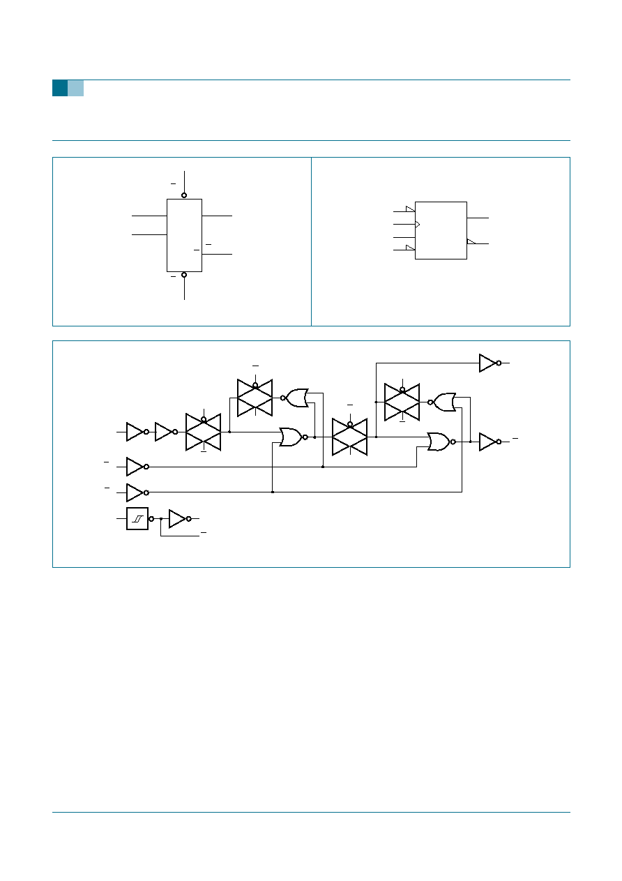
6.
Functional diagram
Fig 1.
Logic symbol
Fig 2.
IEC logic symbol
mnb139
RD
FF
SD
7
Q
Q
Q
5
2
1
3
Q
SD
CP
CP
D
D
6
RD
mnb140
3
1
2
C1
7
S
1D
6
R
5
Fig 3.
Logic diagram
mna421
SD
CP
RD
D
C
C
Q
C
C
C
C
C
C
Q
C
C

74LVC2G74_1
© Koninklijke Philips Electronics N.V. 2005. All rights reserved.
Product data sheet
Rev. 01 -- 3 November 2005
4 of 20
Philips Semiconductors
74LVC2G74
Single D-type flip-flop with set and reset; positive edge trigger
7.
Pinning information
7.1 Pinning
7.2 Pin description
8.
Functional description
8.1 Function table
[1]
H = HIGH voltage level;
L = LOW voltage level;
X = don't care.
Fig 4.
Pin configuration TSSOP8 and
VSSOP8
Fig 5.
Pin configuration XSON8
74
CP
V
CC
D
SD
Q
RD
GND
Q
001aab659
1
2
3
4
6
5
8
7
74
RD
SD
V
CC
Q
Q
D
CP
GND
001aab658
3
6
2
7
1
8
4
5
Transparent top view
Table 4:
Pin description
Symbol
Pin
Description
CP
1
clock input (LOW-to-HIGH, edge-triggered)
D
2
data input
Q
3
complement flip-flop output
GND
4
ground (0 V)
Q
5
true flip-flop output
RD
6
asynchronous reset-direct input (active LOW)
SD
7
asynchronous set-direct input (active LOW)
V
CC
8
supply voltage
Table 5:
Function table for asynchronous operation
[1]
Input
Output
SD
RD
CP
D
Q
Q
L
H
X
X
H
L
H
L
X
X
L
H
L
L
X
X
H
H

74LVC2G74_1
© Koninklijke Philips Electronics N.V. 2005. All rights reserved.
Product data sheet
Rev. 01 -- 3 November 2005
5 of 20
Philips Semiconductors
74LVC2G74
Single D-type flip-flop with set and reset; positive edge trigger
[1]
H = HIGH voltage level;
L = LOW voltage level;
X = don't care;
= LOW-to-HIGH CP transition;
Q
n+1
= state after the next LOW-to-HIGH CP transition.
9.
Limiting values
[1]
The input and output voltage ratings may be exceeded if the input and output current ratings are observed.
[2]
When V
CC
= 0 V (Power-down mode), the output voltage can be 5.5 V in normal operation.
10. Recommended operating conditions
Table 6:
Function table for synchronous operation
[1]
Input
Output
SD
RD
CP
D
Q
n+1
Q
n+1
H
H
L
L
H
H
H
H
H
L
Table 7:
Limiting values
In accordance with the Absolute Maximum Rating System (IEC 60134). Voltages are referenced to
GND (ground = 0 V).
Symbol
Parameter
Conditions
Min
Max
Unit
V
CC
supply voltage
-
0.5
+6.5
V
I
IK
input clamping current
V
I
< 0 V
-
-
50
mA
V
I
input voltage
[1]
-
0.5
+6.5
V
I
OK
output clamping current V
O
> V
CC
or V
O
< 0 V
-
±
50
mA
V
O
output voltage
active mode
[1] [2]
-
0.5
V
CC
+ 0.5 V
Power-down mode
[1] [2]
-
0.5
+6.5
V
I
O
output current
V
O
= 0 V to V
CC
-
±
50
mA
I
CC
quiescent supply
current
-
±
100
mA
I
GND
ground current
-
±
100
mA
T
stg
storage temperature
-
65
+150
∞
C
P
tot
total power dissipation
T
amb
=
-
40
∞
C to +125
∞
C
-
250
mW
Table 8:
Recommended operating conditions
Symbol
Parameter
Conditions
Min
Typ
Max
Unit
V
CC
supply voltage
1.65
-
5.5
V
V
I
input voltage
0
-
5.5
V
V
O
output voltage
active mode
0
-
V
CC
V
Power-down mode;
V
CC
= 0 V
0
-
5.5
V
T
amb
ambient temperature
-
40
-
+125
∞
C
t
/
V
input transition rise and
fall rate
V
CC
= 1.65 V to 2.7 V
0
-
20
ns/V
V
CC
= 2.7 V to 5.5 V
0
-
10
ns/V