 | ÐлекÑÑоннÑй компоненÑ: 74LVC374A | СкаÑаÑÑ:  PDF PDF  ZIP ZIP |
Äîêóìåíòàöèÿ è îïèñàíèÿ www.docs.chipfind.ru
Philips
Semiconductors
74LVC374A
Octal D-type flip-flop with 5-volt tolerant
inputs/outputs; positive edge-trigger
(3-State)
Product specification
1998 Jul 29
INTEGRATED CIRCUITS
Philips Semiconductors
Product specification
74LVC374A
Octal D-type flip-flop with 5-volt tolerant
inputs/outputs; positive edge-trigger (3-State)
2
1998 Jul 29
853-1861 19802
FEATURES
·
5-volt tolerant inputs/outputs, for interfacing with 5-volt logic
·
Supply voltage range of 2.7V to 3.6V
·
Complies with JEDEC standard no. 8-1A
·
CMOS low power consumption
·
Direct interface with TTL levels
·
High impedance when V
CC
= 0V
·
8-bit positive edge-triggered register
·
Independent register and 3-State buffer operation
DESCRIPTION
The 74LVC374A is a high-performance, low-power, low-voltage,
Si-gate CMOS device, superior to most advanced CMOS
compatible TTL families.
Inputs can be driven from either 3.3V or 5V devices. In 3-State
operation, outputs can handle 5V. This feature allows the use of
these devices as translators in a mixed 3.3V/5V environment.
The 74LVC374A is an octal D-type flip-flop featuring separate
D-type inputs for each flip-flop and 3-State outputs for bus-oriented
applications. A clock (CP) and an output enable (OE) input are
common to all flip-flops.
The eight flip-flops will store the state of their individual D-inputs
that meet the setup and hold times requirements on the
LOW-to-HIGH CP transition.
When OE is LOW, the contents of the eight flip-flops is available at
the outputs. When OE is HIGH, the outputs go to the high
impedance OFF-state. Operation of the OE input does not affect the
state of the flip-flops.
The '374' is functionally identical to the '574', but the '574' has a
different pin arrangement.
QUICK REFERENCE DATA
GND = 0V; T
amb
=25
°
C; t
r
= t
f
v
2.5ns
SYMBOL
PARAMETER
CONDITIONS
TYPICAL
UNIT
t
PHL
/t
PLH
Propagation delay
CP to Q
n
C
L
= 50pF
V
CC
= 3.3V
4.8
ns
f
max
maximum clock frequency
150
MHz
C
I
Input capacitance
5.0
pF
C
PD
Power dissipation capacitance per
flip-flop
Notes 1 and 2
20
pF
NOTE:
1. C
PD
is used to determine the dynamic power dissipation (P
D
in
m
W):
P
D
= C
PD
x V
CC
2
x f
i
+
S
(C
L
x V
CC
2
x f
o
) where:
f
i
= input frequency in MHz; C
L
= output load capacity in pF;
f
o
= output frequency in MHz; V
CC
= supply voltage in V;
S
(C
L
x V
CC
2
x f
o
) = sum of outputs.
2. The condition is V
I
= GND to V
CC
ORDERING INFORMATION
PACKAGES
TEMPERATURE
RANGE
OUTSIDE
NORTH AMERICA
NORTH AMERICA
PKG. DWG. #
20-Pin Plastic Shrink Small Outline (SO)
40
°
C to +85
°
C
74LVC374A D
74LVC374A D
SOT163-1
20-Pin Plastic Shrink Small Outline (SSOP) Type II
40
°
C to +85
°
C
74LVC374A DB
74LVC374A DB
SOT339-1
20-Pin Plastic Thin Shrink Small Outline (TSSOP) Type I
40
°
C to +85
°
C
74LVC374A PW
7LVC374APW DH
SOT360-1
Philips Semiconductors
Product specification
74LVC374A
Octal D-type flip-flop with 5-volt tolerant
inputs/outputs; positive edge-trigger (3-State)
1998 Jul 29
3
PIN CONFIGURATION
1
2
3
4
5
6
7
8
9
10
11
12
13
14
15
16
17
18
19
20
OE
Q0
D0
D1
Q1
Q2
D2
D3
Q3
Q4
GND
D4
D5
Q5
Q6
D6
D7
Q7
V
CC
CP
SA00389
PIN DESCRIPTION
PIN NUMBER
SYMBOL
FUNCTION
1
OE
Output enable input (active-Low)
3, 4, 7, 8, 13,
14, 17, 18
D0-D7
Data inputs
2, 5, 6, 9, 12,
15, 16, 19
Q0-Q7
3-state flip-flop outputs
11
CP
Clock input (LOW-to-HIGH,
edge-triggered)
10
GND
Ground (0V)
20
V
CC
Positive supply voltage
LOGIC SYMBOL
3
4
7
8
13
14
18
17
2
5
6
9
12
15
16
19
1
11
SA00390
D0
D1
D2
D3
D4
D5
D6
D7
Q0
Q1
Q2
Q3
Q4
Q5
Q6
Q7
OE
CP
LOGIC SYMBOL (IEEE/IEC)
11
3
2
4
5
7
6
8
9
C1
13
12
14
15
17
16
18
19
1
EN1
1D
SA00391
FUNCTIONAL DIAGRAM
1
2
3
4
5
6
7
8
9
11
12
13
14
15
16
17
18
19
OE
Q0
D0
D1
Q1
Q2
D2
D3
Q3
Q4
D4
D5
Q5
Q6
D6
D7
Q7
CP
FF1
to
FF8
3-State
OUTPUTS
SA00392
Philips Semiconductors
Product specification
74LVC374A
Octal D-type flip-flop with 5-volt tolerant
inputs/outputs; positive edge-trigger (3-State)
1998 Jul 29
4
LOGIC DIAGRAM
Q
D
D0
Q0
D
D1
D
D2
D
D3
D
D4
D
D5
D
D6
D
D7
Q1
Q2
Q3
Q4
Q5
Q6
Q7
CP
OE
Q
Q
Q
Q
Q
Q
Q
SA00393
CP
CP
CP
CP
CP
CP
CP
CP
FF1
FF2
FF3
FF4
FF5
FF6
FF7
FF8
FUNCTION TABLE
OPERATING MODES
INPUTS
INTERNAL FLIP-FLOPS
OUTPUTS
OPERATING MODES
OE
LE
D
n
INTERNAL FLIP-FLOPS
Q
0
to Q
7
Load and read register
L
L
°
°
l
h
L
H
L
H
Load register and
disable outputs
H
H
°
°
l
h
L
H
Z
Z
H = HIGH voltage level
h
= HIGH voltage level one setup time prior to the LOW-to-HIGH CP transition
L
= LOW voltage level
l
= LOW voltage level one setup time prior to the LOW-to-HIGH CP transition
Z = High impedance OFF-state
°
= LOW-to-HIGH clock transition
Philips Semiconductors
Product specification
74LVC374A
Octal D-type flip-flop with 5-volt tolerant
inputs/outputs; positive edge-trigger (3-State)
1998 Jul 29
5
RECOMMENDED OPERATING CONDITIONS
SYMBOL
PARAMETER
CONDITIONS
LIMITS
UNIT
SYMBOL
PARAMETER
CONDITIONS
MIN
MAX
UNIT
V
CC
DC supply voltage (for max. speed performance)
2.7
3.6
V
V
CC
DC supply voltage (for low-voltage applications)
1.2
3.6
V
V
I
DC input voltage range
0
5.5
V
V
O
DC output voltage range; output HIGH or LOW
state
0
V
CC
V
O
DC output voltage range; output 3-State
0
5.5
T
amb
Operating ambient temperature range in free-air
40
+85
°
C
t
r
, t
f
Input rise and fall times
V
CC
= 1.2 to 2.7V
V
CC
= 2.7 to 3.6V
0
0
20
10
ns/V
ABSOLUTE MAXIMUM RATINGS
1
In accordance with the Absolute Maximum Rating System (IEC 134)
Voltages are referenced to GND (ground = 0V)
SYMBOL
PARAMETER
CONDITIONS
RATING
UNIT
V
CC
DC supply voltage
0.5 to +6.5
V
I
IK
DC input diode current
V
I
t
0
50
mA
V
I
DC input voltage
Note 2
0.5 to +6.5
V
I
OK
DC output diode current
V
O
u
V
CC
or V
O
t
0
"
50
mA
V
O
DC output voltage; output HIGH or LOW state
Note 2
0.5 to V
CC
+0.5
V
V
O
DC output voltage; output 3-State
Note 2
0.5 to 6.5
V
I
O
DC output source or sink current
V
O
= 0 to V
CC
"
50
mA
I
GND
, I
CC
DC V
CC
or GND current
"
100
mA
T
stg
Storage temperature range
65 to +150
°
C
Power dissipation per package
P
TOT
plastic mini-pack (SO)
above +70
°
C derate linearly with 8 mW/K
500
mW
plastic shrink mini-pack (SSOP and TSSOP)
above +60
°
C derate linearly with 5.5 mW/K
500
mW
NOTES:
1. Stresses beyond those listed may cause permanent damage to the device. These are stress ratings only and functional operation of the
device at these or any other conditions beyond those indicated under "recommended operating conditions" is not implied. Exposure to
absolute-maximum-rated conditions for extended periods may affect device reliability.
2. The input and output voltage ratings may be exceeded if the input and output current ratings are observed.
Philips Semiconductors
Product specification
74LVC374A
Octal D-type flip-flop with 5-volt tolerant
inputs/outputs; positive edge-trigger (3-State)
1998 Jul 29
6
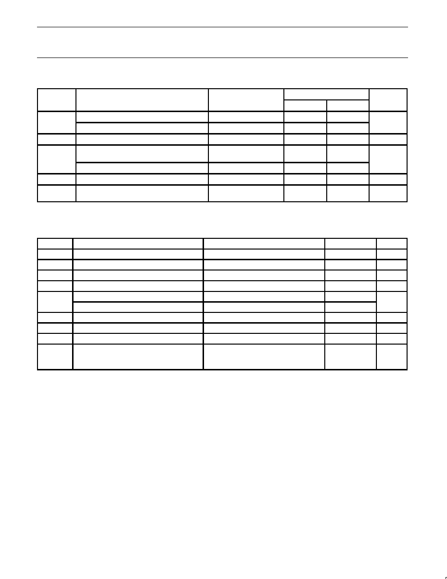
DC ELECTRICAL CHARACTERISTICS
Over recommended operating conditions voltages are referenced to GND (ground = 0V)
LIMITS
SYMBOL
PARAMETER
TEST CONDITIONS
Temp = -40
°
C to +85
°
C
UNIT
MIN
TYP
1
MAX
V
HIGH level Input voltage
V
CC
= 1.2V
V
CC
V
V
IH
HIGH level Input voltage
V
CC
= 2.7 to 3.6V
2.0
V
V
LOW level Input voltage
V
CC
= 1.2V
GND
V
V
IL
LOW level Input voltage
V
CC
= 2.7 to 3.6V
0.8
V
V
CC
= 2.7V; V
I
= V
IH
or V
IL
; I
O
= 12mA
V
CC
*
0.5
V
O
HIGH level output voltage
V
CC
= 3.0V; V
I
= V
IH
or V
IL
; I
O
= 100
µ
A
V
CC
*
0.2
V
CC
V
V
OH
HIGH level output voltage
V
CC
= 3.0V; V
I
= V
IH
or V
IL;
I
O
= 18mA
V
CC
*
0.6
V
V
CC
= 3.0V; V
I
= V
IH
or V
IL;
I
O
= 24mA
V
CC
*
0.8
V
CC
= 2.7V; V
I
= V
IH
or V
IL
; I
O
= 12mA
0.40
V
OL
LOW level output voltage
V
CC
= 3.0V; V
I
= V
IH
or V
IL
; I
O
= 100
µ
A
GND
0.20
V
V
CC
= 3.0V; V
I
= V
IH
or V
IL;
I
O
= 24mA
0.55
I
Input leakage current
2
V
= 3 6V; V = 5 5V or GND
"
0 1
"
5
µ
A
I
I
Input leakage current
2
V
CC
= 3.6V; V
I
= 5.5V or GND
"
0.1
"
5
µ
A
I
OZ
3-State output OFF-state current
V
CC
= 3.6V; V
I
= V
IH
or V
IL
; V
O
= 5.5V or GND
0.1
"
10
µ
A
I
off
Power off leakage supply
V
CC
= 0.0V; V
I
or V
O
= 5.5V
0.1
"
10
µ
A
I
CC
Quiescent supply current
V
CC
= 3.6V; V
I
= V
CC
or GND; I
O
= 0
0.1
10
µ
A
I
CC
Additional quiescent supply current
per input pin
V
CC
= 2.7V to 3.6V; V
I
= V
CC
0.6V; I
O
= 0
5
500
µ
A
NOTES:
1. All typical values are at V
CC
= 3.3V and T
amb
= 25
°
C.
2. The specified overdrive current at the data input forces the data input to the opposite logic input state.
AC CHARACTERISTICS
GND = 0V; t
r
= t
f
v
2.5ns; C
L
= 50pF; R
L
= 500
; T
amb
= 40
°
C to +85
°
C.
LIMITS
SYMBOL
PARAMETER
WAVEFORM
V
CC
= 3.3V
±
0.3V
V
CC
= 2.7V
V
CC
= 1.2V
UNIT
MIN
TYP
1
MAX
MIN
MAX
TYP
t
PHL
t
PLH
Propagation delay
CP to Q
n
1, 4
1.5
4.8
7.0
1.5
8.0
21
ns
t
PZH
t
PZL
3-State output enable time
OE to Q
n
2, 4
1.5
4.8
7.5
1.5
8.5
22
ns
t
PHZ
t
PLZ
3-State output disable time
OE to Q
n
2, 4
1.5
4.3
6.0
1.5
7.0
15
ns
t
W
Clock pulse width HIGH or LOW
1
3.0
1.5
3.0
ns
t
SU
Setup time
D
n
to CP
3
2.0
0
2.0
ns
t
h
Hold time
D
n
to CP
3
1.5
0.6
1.5
ns
f
max
maximum clock pulse frequency
1
100
80
MHz
NOTE:
1. Unless otherwise stated, all typical values are at V
CC
= 3.3V and T
amb
= 25
°
C.
Philips Semiconductors
Product specification
74LVC374A
Octal D-type flip-flop with 5-volt tolerant
inputs/outputs; positive edge-trigger (3-State)
1998 Jul 29
7
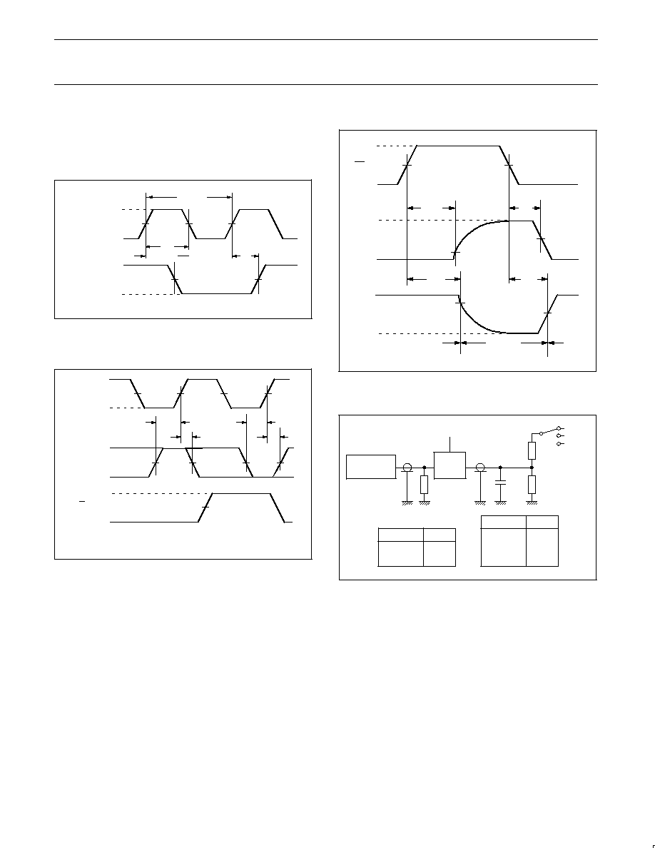
AC WAVEFORMS
V
M
= 1.5V at V
CC
w
2.7V; V
M
= 0.5 V
CC
at V
CC
t
2.7V.
V
OL
and V
OH
are the typical output voltage drop that occur with the
output load.
V
X
= V
OL
+ 0.3V at V
CC
w
2.7V; V
X
= V
OL
+ 0.1 V
CC
at V
CC
t
2.7V
V
Y
= V
OH
0.3V at V
CC
w
2.7V; V
Y
= V
OH
0.1 V
CC
at V
CC
t
2.7V
t
w
t
PLH
CP INPUT
Qn OUTPUT
V
M
V
M
V
M
V
M
V
M
V
I
GND
V
OH
V
OL
SA00394
t
PHL
1/f
max
Waveform 1. Clock (CP) to output (Q
n
) propagation delays, the
clock pulse width, output transition times and the maximum
clock pulse frequency.
VM
SW00107
V
I
GND
ÉÉÉÉ
ÉÉÉÉ
ÉÉÉÉ
ÉÉÉÉÉÉÉ
ÉÉÉÉÉÉÉ
ÉÉÉÉÉÉÉ
ÉÉ
ÉÉ
ÉÉ
V
M
Dn
INPUT
V
I
GND
VM
V
OH
Qn
OUTPUT
V
OL
CP
INPUT
t
su
t
h
t
su
t
h
NOTE: The shaded areas indicate when the input is permitted to change
for predictable output performance.
Waveform 2. Data setup and hold times for the D
n
input to the
CP input.
t
PLZ
t
PZL
V
I
nOE INPUT
GND
V
CC
Q
n
OUTPUT
LOW-to-OFF
OFF-to-LOW
V
OL
V
OH
Q
n
OUTPUT
HIGH-to-OFF
OFF-to-HIGH
GND
outputs
enabled
outputs
enabled
outputs
disabled
t
PHZ
V
M
V
M
V
M
t
PZH
V
X
V
Y
SW00207
Waveform 3. 3-State enable and disable times.
TEST CIRCUIT
PULSE
GENERATOR
V
I
R
T
D.U.T.
V
O
C
L
50pF
S
1
2 x V
CC
Open
GND
500
500
V
CC
V
I
t
2.7V
V
CC
2.7V 3.6V
2.7V
Test
S
1
GND
t
PLZ
/t
PZL
2 x V
CC
t
PHZ
/t
PZH
t
PLH
/t
PHL
Open
SY00003
V
CC
Waveform 4. Load circuitry for switching times.
Philips Semiconductors
Product specification
74LVC374A
Octal D-type flip-flop with 5-volt tolerant
inputs/outputs; positive edge-trigger (3-State)
1998 Jul 29
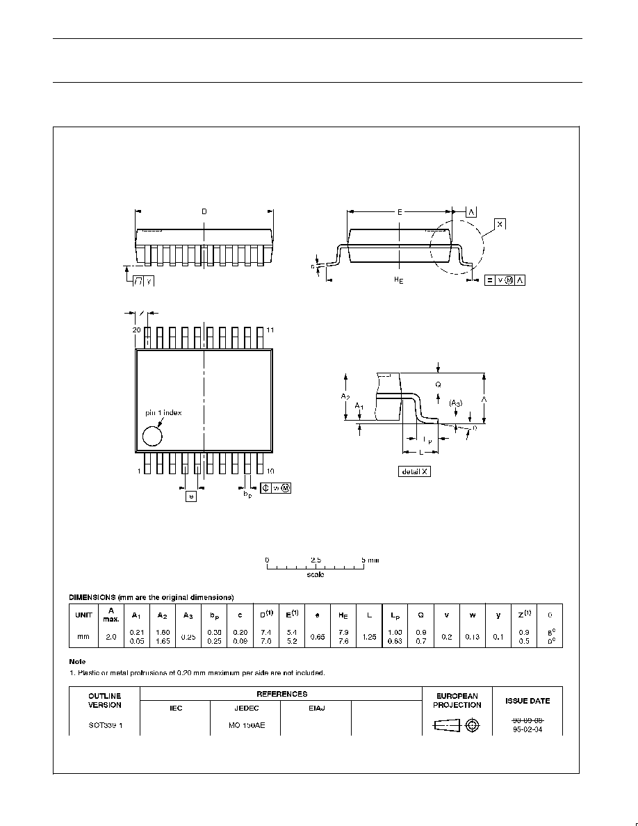
8
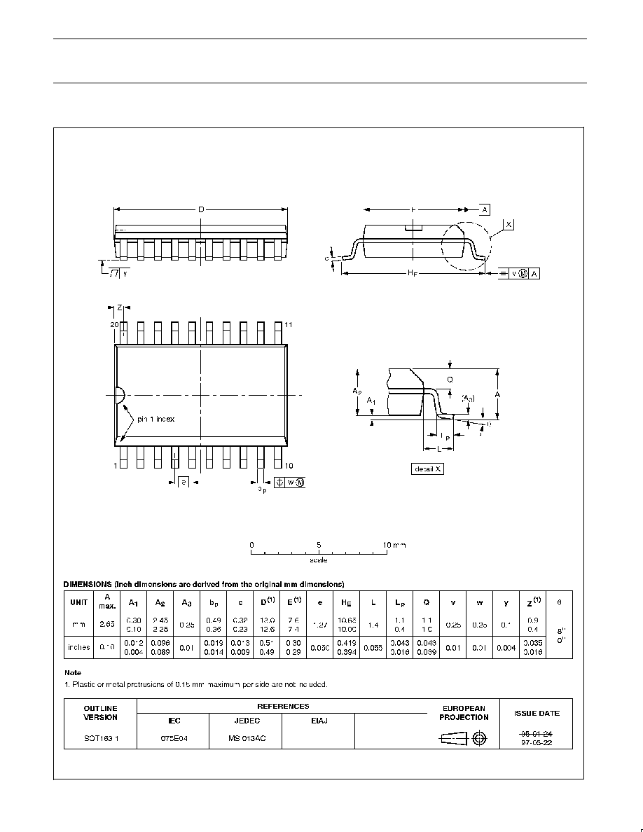
SO20:
plastic small outline package; 20 leads; body width 7.5 mm
SOT163-1
Philips Semiconductors
Product specification
74LVC374A
Octal D-type flip-flop with 5-volt tolerant
inputs/outputs; positive edge-trigger (3-State)
1998 Jul 29
9
SSOP20:
plastic shrink small outline package; 20 leads; body width 5.3 mm
SOT339-1
Philips Semiconductors
Product specification
74LVC374A
Octal D-type flip-flop with 5-volt tolerant
inputs/outputs; positive edge-trigger (3-State)
1998 Jul 29
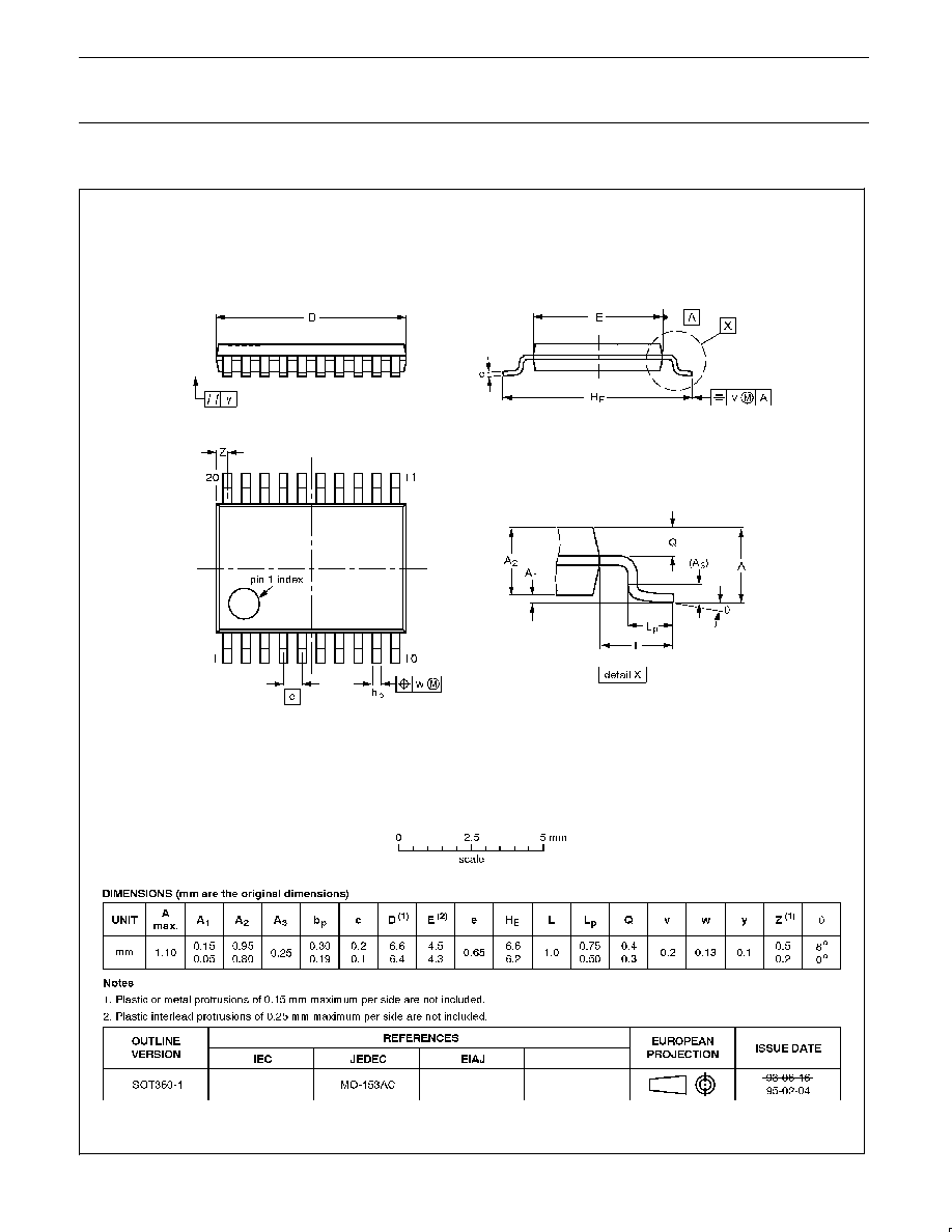
10
TSSOP20:
plastic thin shrink small outline package; 20 leads; body width 4.4 mm
SOT360-1

Philips Semiconductors
Product specification
74LVC374A
Octal D-type flip-flop with 5-volt tolerant
inputs/outputs; positive edge-trigger (3-State)
1998 Jul 29
11
NOTES
Philips Semiconductors
Product specification
74LVC374A
Octal D-type flip-flop with 5-volt tolerant
inputs/outputs; positive edge-trigger (3-State)
yyyy mmm dd
12
Definitions
Short-form specification -- The data in a short-form specification is extracted from a full data sheet with the same type number and title. For
detailed information see the relevant data sheet or data handbook.
Limiting values definition -- Limiting values given are in accordance with the Absolute Maximum Rating System (IEC 134). Stress above one
or more of the limiting values may cause permanent damage to the device. These are stress ratings only and operation of the device at these or
at any other conditions above those given in the Characteristics sections of the specification is not implied. Exposure to limiting values for extended
periods may affect device reliability.
Application information -- Applications that are described herein for any of these products are for illustrative purposes only. Philips
Semiconductors make no representation or warranty that such applications will be suitable for the specified use without further testing or
modification.
Disclaimers
Life support -- These products are not designed for use in life support appliances, devices or systems where malfunction of these products can
reasonably be expected to result in personal injury. Philips Semiconductors customers using or selling these products for use in such applications
do so at their own risk and agree to fully indemnify Philips Semiconductors for any damages resulting from such application.
Right to make changes -- Philips Semiconductors reserves the right to make changes, without notice, in the products, including circuits, standard
cells, and/or software, described or contained herein in order to improve design and/or performance. Philips Semiconductors assumes no
responsibility or liability for the use of any of these products, conveys no license or title under any patent, copyright, or mask work right to these
products, and makes no representations or warranties that these products are free from patent, copyright, or mask work right infringement, unless
otherwise specified.
Philips Semiconductors
811 East Arques Avenue
P.O. Box 3409
Sunnyvale, California 940883409
Telephone 800-234-7381
©
Copyright Philips Electronics North America Corporation 1998
All rights reserved. Printed in U.S.A.
print code
Date of release: 08-98
Document order number:
9397-750-04507
Philips
Semiconductors
Data sheet
status
Objective
specification
Preliminary
specification
Product
specification
Product
status
Development
Qualification
Production
Definition
[1]
This data sheet contains the design target or goal specifications for product development.
Specification may change in any manner without notice.
This data sheet contains preliminary data, and supplementary data will be published at a later date.
Philips Semiconductors reserves the right to make chages at any time without notice in order to
improve design and supply the best possible product.
This data sheet contains final specifications. Philips Semiconductors reserves the right to make
changes at any time without notice in order to improve design and supply the best possible product.
Data sheet status
[1]
Please consult the most recently issued datasheet before initiating or completing a design.