
2004 Mar 22
2
Philips Semiconductors
Product specification
Quad 2-input NAND gate (open drain)
74LVC38A
FEATURES
∑
5 V tolerant inputs for interfacing with 5 V logic
∑
Wide supply voltage range from 1.2 to 3.6 V
∑
CMOS low power consumption
∑
Direct interface with TTL levels
∑
Open-drain outputs
∑
Inputs accept voltages up to 5.5 V
∑
Complies with JEDEC standard no. 8-1A
∑
Specified from
-
40 to +85
∞
C and
-
40 to +125
∞
C.
DESCRIPTION
The 74LVC38A is a high-performance, low-power,
low-voltage, Si-gate CMOS device, superior to most
advanced CMOS compatible TTL families.
Inputs can be driven from either 3.3 or 5 V devices. This
feature allows the use of these devices as translators in a
mixed 3.3 and 5 V environment.
The 74LVC38A provides the 2-input NAND function.
The outputs of the 74LVC38A devices are open drain and
can be connected to other open-drain outputs to
implement active-LOW wired-OR or active-HIGH
wired-AND functions.
QUICK REFERENCE DATA
GND = 0 V; T
amb
= 25
∞
C; t
r
= t
f
2.5 ns.
Notes
1. C
PD
is used to determine the dynamic power dissipation (P
D
in
µ
W).
P
D
= C
PD
◊
V
CC
2
◊
f
i
◊
N +
(C
L
◊
V
CC
2
◊
f
o
) where:
f
i
= input frequency in MHz;
f
o
= output frequency in MHz;
C
L
= output load capacitance in pF;
V
CC
= supply voltage in Volts;
N = total load switching outputs;
(C
L
◊
V
CC
2
◊
f
o
) = sum of the outputs.
2. The condition is V
I
= GND to V
CC
.
ORDERING INFORMATION
SYMBOL
PARAMETER
CONDITIONS
TYPICAL
UNIT
t
PZL
propagation delay nA, nB to nY
C
L
= 50 pF; V
CC
= 3.3 V
1.7
ns
t
PLZ
propagation delay nA, nB to nY
C
L
= 50 pF; V
CC
= 3.3 V
2.3
ns
C
I
input capacitance
4.0
pF
C
PD
power dissipation capacitance per gate
V
CC
= 3.3 V; notes 1 and 2
5.5
pF
TYPE NUMBER
PACKAGE
TEMPERATURE RANGE
PINS
PACKAGE
MATERIAL
CODE
74LVC38AD
-
40 to +125
∞
C
14
SO14
plastic
SOT108-1
74LVC38ADB
-
40 to +125
∞
C
14
SSOP14
plastic
SOT337-1
74LVC38APW
-
40 to +125
∞
C
14
TSSOP14
plastic
SOT402-1
74LVC38ABQ
-
40 to +125
∞
C
14
DHVQFN14
plastic
SOT762-1

2004 Mar 22
3
Philips Semiconductors
Product specification
Quad 2-input NAND gate (open drain)
74LVC38A
FUNCTION TABLE
See note 1.
Note
1. H = HIGH voltage level;
L = LOW voltage level:
Z = high-impedance OFF-state.
PINNING
INPUTS
OUTPUTS
nA
nB
nY
L
L
Z
L
H
Z
H
L
Z
H
H
L
PIN
SYMBOL
DESCRIPTION
1
1A
data input
2
1B
data input
3
1Y
data output
4
2A
data input
5
2B
data input
6
2Y
data output
7
GND
ground (0 V)
8
3Y
data output
9
3A
data input
10
3B
data input
11
4Y
data output
12
4A
data input
13
4B
data input
14
V
CC
supply voltage
2004 Mar 22
4
Philips Semiconductors
Product specification
Quad 2-input NAND gate (open drain)
74LVC38A
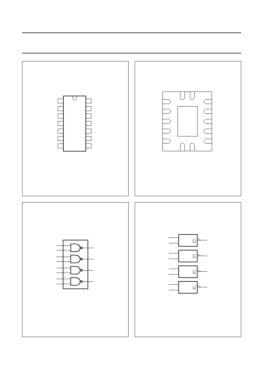
handbook, halfpage
MNA696
38
1
2
3
4
5
6
7
8
14
13
12
11
10
9
1A
1B
1Y
2A
2B
2Y
GND
3Y
3A
3B
4Y
4A
4B
VCC
Fig.1 Pin configuration SO14 and (T)SSOP14.
handbook, halfpage
1
14
GND
(1)
1A
VCC
7
2
3
4
5
6
1B
1Y
2A
2B
2Y
13
12
11
10
9
4B
4A
4Y
3B
3A
8
GND
Top view
3Y
MNA977
Fig.2 Pin configuration (DHVQFN14).
(1) The die substrate is attached to this pad using conductive die
attach material. It can not be used as a supply pin or input.
handbook, halfpage
MNA697
1A
1B
1Y
2
1
3
2A
2B
2Y
5
4
6
3A
3B
3Y
10
9
8
4A
4B
4Y
13
12
11
Fig.3 Logic symbol.
handbook, halfpage
2
3
&
1
5
6
&
4
10
8
&
9
MNA698
13
11
&
12
Fig.4 Logic symbol (IEEE/IEC).

2004 Mar 22
5
Philips Semiconductors
Product specification
Quad 2-input NAND gate (open drain)
74LVC38A
Fig.5 Logic diagram (one gate).
handbook, halfpage
MNA699
Y
GND
A
B
RECOMMENDED OPERATING CONDITIONS
LIMITING VALUES
In accordance with the Absolute Maximum Rating System (IEC 60134); voltages are referenced to GND (ground = 0 V).
Notes
1. The input and output voltage ratings may be exceeded if the input and output current ratings are observed.
2. For SO14 packages: above 70
∞
C derate linearly with 8 mW/K.
For (T)SSOP14 packages: above 60
∞
C derate linearly with 5.5 mW/K.
For DHVQFN14 packages: above 60
∞
C derate linearly with 4.5 mW/K.
SYMBOL
PARAMETER
CONDITIONS
MIN.
MAX.
UNIT
V
CC
supply voltage
for maximum speed performance
2.7
3.6
V
for low-voltage applications
1.2
3.6
V
V
I
input voltage
0
5.5
V
V
O
output voltage
0
5.5
V
T
amb
operating ambient temperature
-
40
+125
∞
C
t
r
, t
f
input rise and fall times
V
CC
= 1.2 to 2.7 V
0
20
ns/V
V
CC
= 2.7 to 3.6 V
0
10
ns/V
SYMBOL
PARAMETER
CONDITIONS
MIN.
MAX.
UNIT
V
CC
supply voltage
-
0.5
+6.5
V
I
IK
input diode current
V
I
< 0
-
-
50
mA
V
I
input voltage
note 1
-
0.5
+6.5
V
I
OK
output diode current
V
O
< 0
-
-
50
mA
V
O
output voltage
note 1
-
0.5
+6.5
V
I
O
output sink current
V
O
= 0 to V
CC
-
50
mA
I
CC
, I
GND
V
CC
or GND current
-
±
100
mA
T
stg
storage temperature
-
65
+150
∞
C
P
tot
power dissipation
T
amb
=
-
40 to +125
∞
C; note 2
-
500
mW
