Philips Semiconductors
Product specification
74LVC573A
Octal D-type transparent latch with 5-volt
tolerant inputs/outputs (3-State)
2
1998 Jul 29
853-1862 19804
FEATURES
·
5-volt tolerant inputs/outputs, for interfacing with 5-volt logic
·
Supply voltage range of 2.7V to 3.6V
·
Complies with JEDEC standard no. 8-1A
·
Inputs accept voltages up to 5.5V
·
CMOS low power consumption
·
Direct interface with TTL levels
·
High impedance when V
CC
= 0V
·
Flow-through pin-out architecture
DESCRIPTION
The 74LVC573A is a high-performance, low-power, low-voltage,
Si-gate CMOS device, superior to most advanced CMOS
compatible TTL families.
Inputs can be driven from either 3.3V or 5V devices. In 3-State
operation, outputs can handle 5V. This feature allows the use of
these devices as translators in a mixed 3.3V/5V environment.
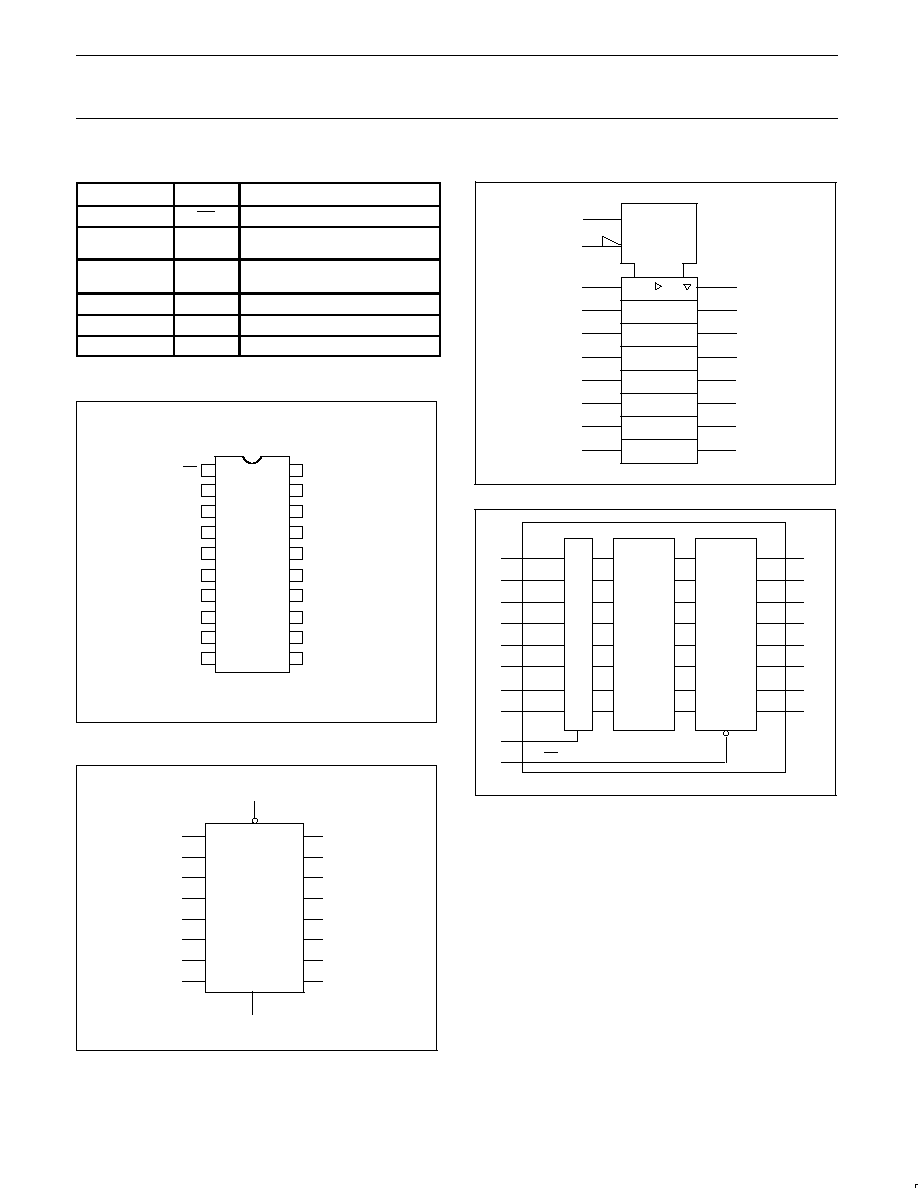
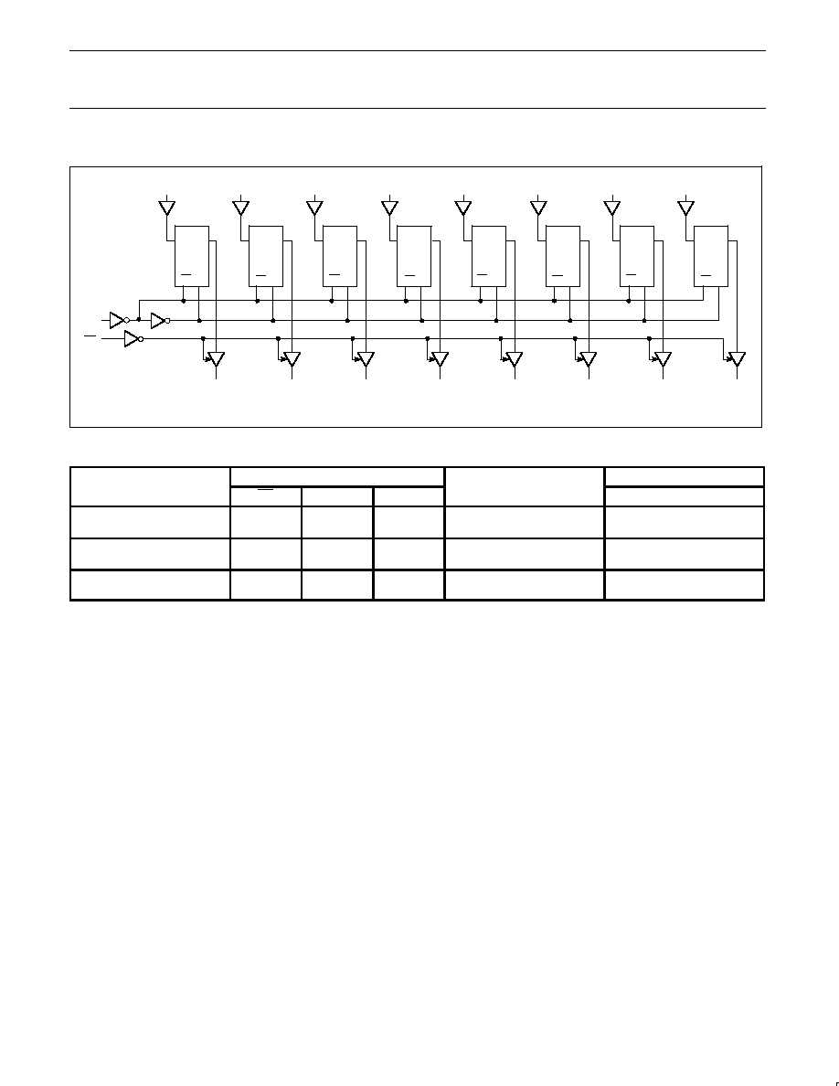
The 74LVC573A is an octal D-type transparent latch featuring
separate D-type inputs for each latch and 3-State outputs for
bus-oriented applications. A latch enable (LE) input and an output
enable (OE) input are common to all internal latches.
The '573A' consists of eight D-type transparent latches with 3-State
true outputs. When LE is HIGH, data at the D
n
inputs enters the
latches. In this condition, the latches are transparent, i.e. a latch
output will change each time its corresponding D-input changes.
When LE is LOW, the latches store the information that was present
at the D-inputs one setup time preceding the HIGH-to-LOW
transition of LE. When OE is LOW, the contents of the eight latches
are available at the outputs. When OE is HIGH, the outputs go to the
high impedance OFF-state. Operation of the OE input does not
affect the state of the latches.
The '573A' is functionally identical to the '373A', but the '373A' has a
different pin arrangement.
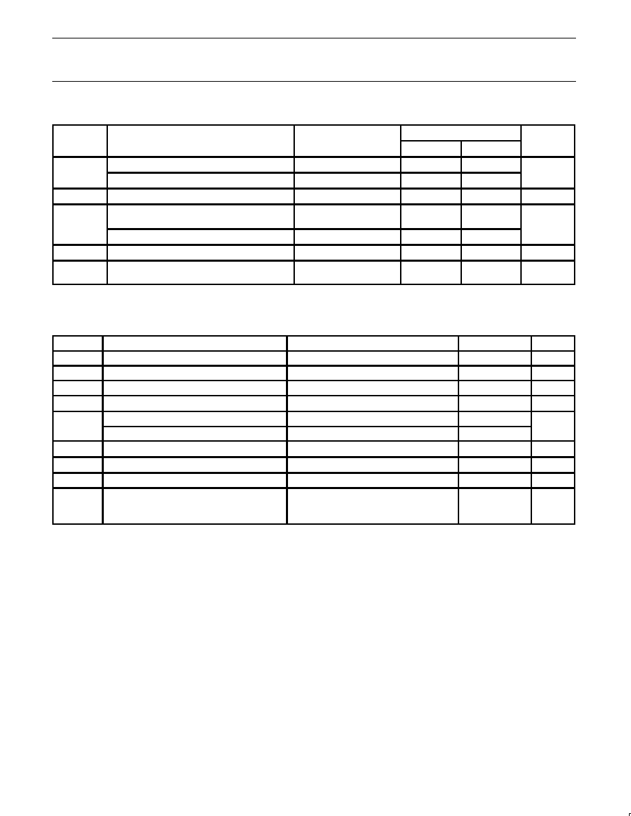
QUICK REFERENCE DATA
SYMBOL
PARAMETER
CONDITIONS
TYPICAL
UNIT
t
PHL
/t
PLH
Propagation delay
D
n
to Q
n;
LE to Q
n
C
L
= 50pF
V
CC
= 3.3V
4.3
4.6
ns
C
I
Input capacitance
5.0
pF
C
PD
Power dissipation capacitance per latch
Notes 1 and 2
20
pF
NOTE:
1. C
PD
is used to determine the dynamic power dissipation (P
D
in
m
W):
P
D
= C
PD
x V
CC
2
x f
i
+
S
(C
L
x V
CC
2
x f
o
) where:
f
i
= input frequency in MHz; C
L
= output load capacity in pF;
f
o
= output frequency in MHz; V
CC
= supply voltage in V;
S
(C
L
x V
CC
2
x f
o
) = sum of outputs.
2. The condition is V
I
= GND to V
CC
ORDERING INFORMATION
PACKAGES
TEMPERATURE
RANGE
OUTSIDE
NORTH AMERICA
NORTH AMERICA
PKG. DWG. #
20-Pin Plastic Shrink Small Outline (SO)
40
°
C to +85
°
C
74LVC573A D
74LVC573A D
SOT163-1
20-Pin Plastic Shrink Small Outline (SSOP) Type II
40
°
C to +85
°
C
74LVC573A DB
74LVC573A DB
SOT339-1
20-Pin Plastic Thin Shrink Small Outline (TSSOP) Type I
40
°
C to +85
°
C
74LVC573A PW
7LVC573APW DH
SOT360-1
Philips Semiconductors
Product specification
74LVC573A
Octal D-type transparent latch with 5-volt
tolerant inputs/outputs (3-State)
1998 Jul 29
5
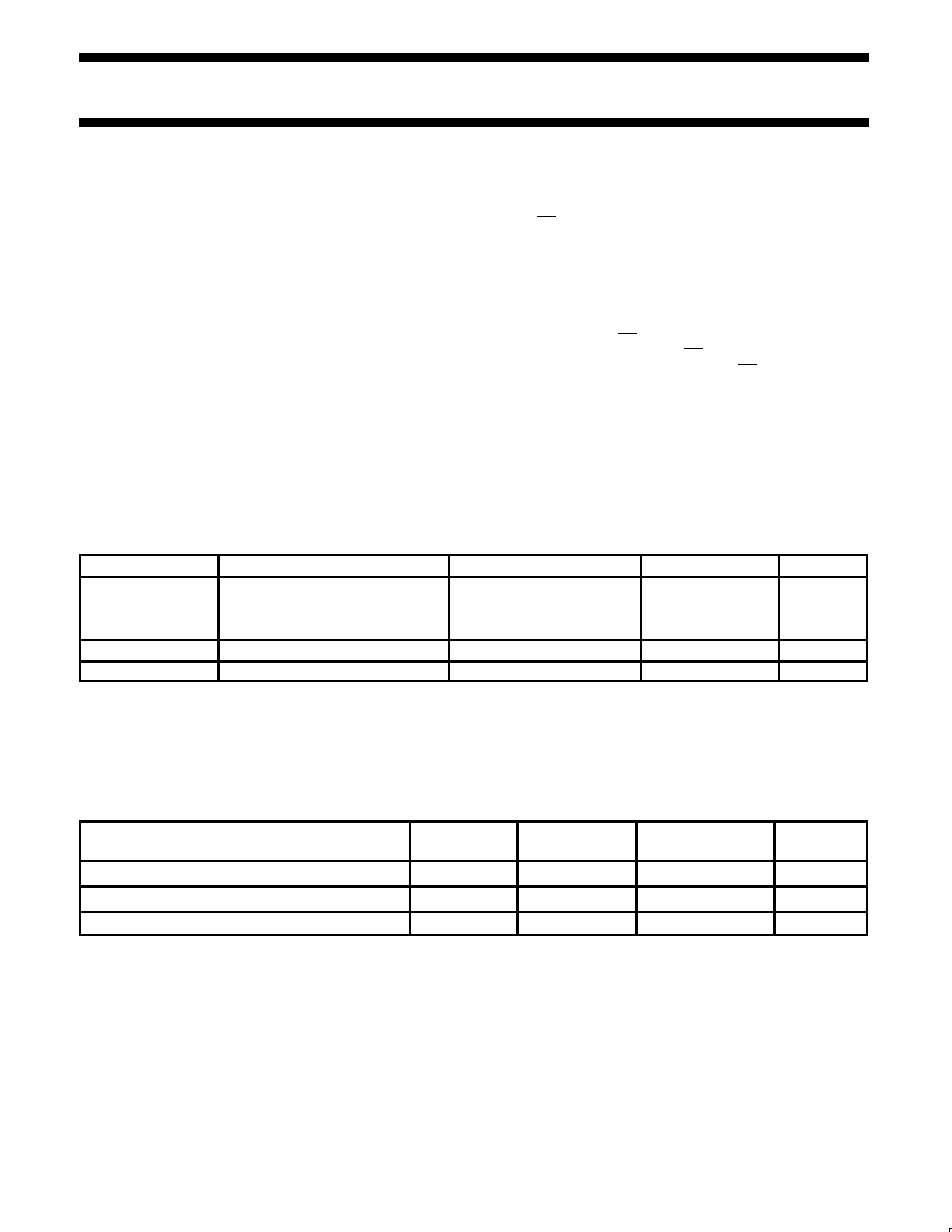
RECOMMENDED OPERATING CONDITIONS
SYMBOL
PARAMETER
CONDITIONS
LIMITS
UNIT
SYMBOL
PARAMETER
CONDITIONS
MIN
MAX
UNIT
V
CC
DC supply voltage (for max. speed performance)
2.7
3.6
V
V
CC
DC supply voltage (for low-voltage applications)
1.2
3.6
V
V
I
DC Input voltage range
0
5.5
V
V
O
DC output voltage range; output HIGH or LOW
state
0
V
CC
V
O
DC output voltage range; output 3-State
0
5.5
T
amb
Operating ambient temperature range in free-air
40
+85
°
C
t
r
, t
f
Input rise and fall times
V
CC
= 1.2 to 2.7V
V
CC
= 2.7 to 3.6V
0
0
20
10
ns/V
ABSOLUTE MAXIMUM RATINGS
1
In accordance with the Absolute Maximum Rating System (IEC 134)
Voltages are referenced to GND (ground = 0V)
SYMBOL
PARAMETER
CONDITIONS
RATING
UNIT
V
CC
DC supply voltage
0.5 to +6.5
V
I
IK
DC input diode current
V
I
t
0
50
mA
V
I
DC input voltage
Note 2
0.5 to +6.5
V
I
OK
DC output diode current
V
O
u
V
CC
or V
O
t
0
"
50
mA
V
O
DC output voltage; output HIGH or LOW state
Note 2
0.5 to V
CC
+0.5
V
V
O
DC output voltage; output 3-State
Note 2
0.5 to 6.5
V
I
O
DC output source or sink current
V
O
= 0 to V
CC
"
50
mA
I
GND
, I
CC
DC V
CC
or GND current
"
100
mA
T
stg
Storage temperature range
65 to +150
°
C
Power dissipation per package
P
TOT
plastic mini-pack (SO)
above +70
°
C derate linearly with 8 mW/K
500
mW
plastic shrink mini-pack (SSOP and TSSOP)
above +60
°
C derate linearly with 5.5 mW/K
500
mW
NOTES:
1. Stresses beyond those listed may cause permanent damage to the device. These are stress ratings only and functional operation of the
device at these or any other conditions beyond those indicated under "recommended operating conditions" is not implied. Exposure to
absolute-maximum-rated conditions for extended periods may affect device reliability.
2. The input and output voltage ratings may be exceeded if the input and output current ratings are observed.