Äîêóìåíòàöèÿ è îïèñàíèÿ www.docs.chipfind.ru
Philips
Semiconductors
74LVC86
Quad 2-input EXCLUSIVE-OR gate
Product specification
Supersedes data of February 1996
IC24 Data Handbook
1997 Mar 18
INTEGRATED CIRCUITS
Philips Semiconductors
Product specification
74LVC86
Quad 2-input EXCLUSIVE-OR gate
2
1997 Mar 18
8531946 17864
FEATURES
·
Wide supply voltage range of 1.2 to 3.6 V
·
In accordance with JEDEC standard no. 8-1A.
·
Inputs accept voltages up to 5.5 V
·
CMOS low power consumption
·
Direct interface with TTL levels
DESCRIPTION
The 74LVC86 is a high-performance, low-power, low-voltage Si-gate
CMOS device that is pin and superior to most advanced CMOS
compatible TTL families.
Inputs can be driven from either 3.3 V or 5 V devices. This feature
allows the use of these devices as translators in a mixed 3.3 V/5 V
environment.
The 74LVC86 provides the 2-input EXCLUSIVE-OR function.
QUICK REFERENCE DATA
GND = 0 V; T
amb
= 25
°
C; t
r
= t
f
2.5 ns
SYMBOL
PARAMETER
CONDITIONS
TYPICAL
UNIT
t
PHL
t
PLH
Propagation delay
nA, nB to nY
C
L
= 15 pF;
V
CC
= 3.3 V
3.7
ns
C
I
Input capacitance
5.0
pF
C
PD
Power dissipation capacitance per gate
V
CC
= 3.3 V, V
I
= GND to V
CC
1
55
pF
NOTE:
1. C
PD
is used to determine the dynamic power dissipation (P
D
in
µ
W)
P
D
= C
PD
×
V
CC
2
×
f
i
)
(C
L
×
V
CC
2
×
f
o
) where:
f
i
= input frequency in MHz; C
L
= output load capacity in pF;
f
o
= output frequency in MHz; V
CC
= supply voltage in V;
(C
L
×
V
CC
2
×
f
o
) = sum of the outputs.
ORDERING INFORMATION
PACKAGES
TEMPERATURE RANGE
OUTSIDE NORTH AMERICA
NORTH AMERICA
PKG. DWG. #
14-Pin Plastic DIL
40
°
C to +85
°
C
74LVC86 N
74LVC86 N
SOT27-1
14-Pin Plastic SO
40
°
C to +85
°
C
74LVC86 D
74LVC86 D
SOT108-1
14-Pin Plastic SSOP Type II
40
°
C to +85
°
C
74LVC86 DB
74LVC86 DB
SOT337-1
14-Pin Plastic TSSOP Type I
40
°
C to +85
°
C
74LVC86 PW
74LVC86PW DH
SOT402-1
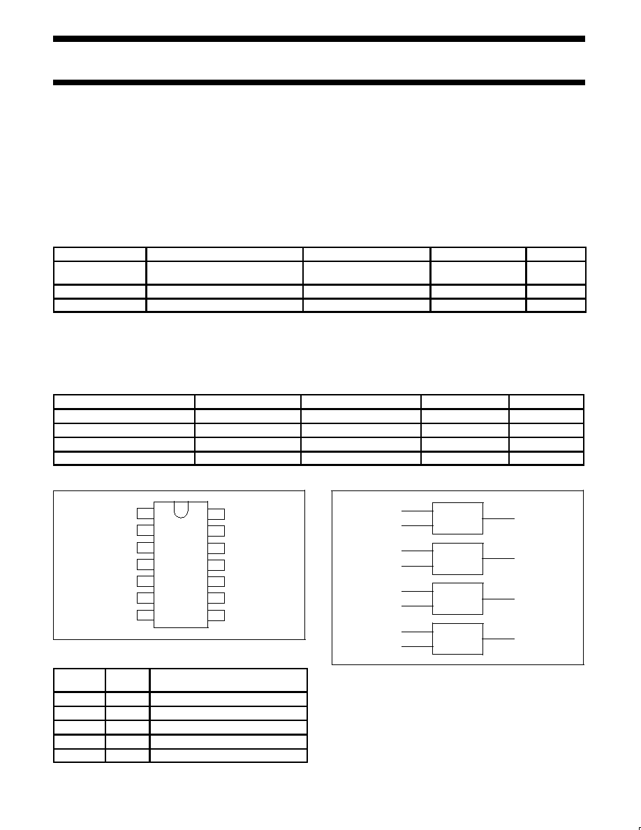
PIN CONFIGURATION
SV00481
1
2
3
4
5
6
7
1A
1B
1Y
2A
2B
2Y
GND
VCC
4B
4A
4Y
3B
3A
3Y
14
13
12
11
10
9
8
PIN DESCRIPTION
PIN
NUMBER
SYMBOL
FUNCTION
1, 4, 9, 12
1A 4A
Data inputs
2, 5, 10, 13
1B 4B
Data inputs
3, 6, 8, 11
1Y 4Y
Data outputs
7
GND
Ground (0 V)
14
V
CC
Positive supply voltage
LOGIC SYMBOL (IEEE/IEC)
SV00479
1
4
9
12
2
5
10
13
3
6
8
11
= 1
= 1
= 1
= 1
Philips Semiconductors
Product specification
74LVC86
Quad 2-input EXCLUSIVE-OR gate
1997 Mar 18
3
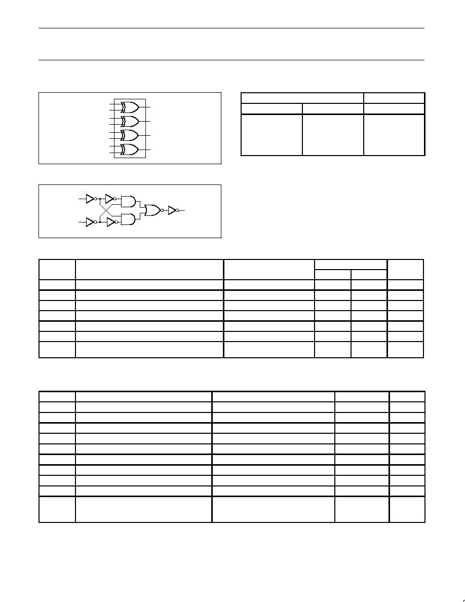
LOGIC SYMBOL
4B
4A
SV00480
1A
1B
2A
2B
3B
3A
1Y
2Y
3Y
4Y
1
2
4
5
13
12
10
9
3
6
11
8
LOGIC DIAGRAM (ONE GATE)
SV00478
A
B
Y
FUNCTION TABLE
INPUTS
OUTPUTS
nA
nB
nY
L
L
L
L
H
H
H
L
H
H
H
L
NOTES:
H = HIGH voltage level
L
= LOW voltage level
RECOMMENDED OPERATING CONDITIONS
SYMBOL
PARAMETER
CONDITIONS
LIMITS
UNIT
SYMBOL
PARAMETER
CONDITIONS
MIN
MAX
UNIT
V
CC
DC supply voltage (for max. speed performance)
2.7
3.6
V
V
CC
DC supply voltage (for low-voltage applications)
1.2
3.6
V
V
I
DC input voltage range
0
5.5
V
V
I/O
DC input voltage range for I/Os
0
V
CC
V
V
O
DC output voltage range
0
V
CC
V
T
amb
Operating free-air temperature range
40
+85
°
C
t
r
, t
f
Input rise and fall times
V
CC
= 1.2 to 2.7V
V
CC
= 2.7 to 3.6V
0
0
20
10
ns/V
ABSOLUTE MAXIMUM RATINGS
1
In accordance with the Absolute Maximum Rating System (IEC 134).
Voltages are referenced to GND (ground = 0V).
SYMBOL
PARAMETER
CONDITIONS
RATING
UNIT
V
CC
DC supply voltage
0.5 to +6.5
V
I
IK
DC input diode current
V
I
t
0
50
mA
V
I
DC input voltage
Note 2
0.5 to +5.5
V
V
I/O
DC input voltage range for I/Os
0.5 to V
CC
+0.5
V
I
OK
DC output diode current
V
O
u
V
CC
or V
O
t
0
"
50
mA
V
OUT
DC output voltage
Note 2
0.5 to V
CC
+0.5
V
I
OUT
DC output source or sink current
V
O
= 0 to V
CC
"
50
mA
I
GND
, I
CC
DC V
CC
or GND current
"
100
mA
T
stg
Storage temperature range
60 to +150
°
C
Power dissipation per package
P
TOT
plastic mini-pack (SO)
above +70
°
C derate linearly with 8 mW/K
500
mW
plastic shrink mini-pack (SSOP and TSSOP)
above +60
°
C derate linearly with 5.5 mW/K
500
mW
NOTES:
1. Stresses beyond those listed may cause permanent damage to the device. These are stress ratings only and functional operation of the
device at these or any other conditions beyond those indicated under "recommended operating conditions" is not implied. Exposure to
absolute-maximum-rated conditions for extended periods may affect device reliability.
2. The input and output voltage ratings may be exceeded if the input and output current ratings are observed.
Philips Semiconductors
Product specification
74LVC86
Quad 2-input EXCLUSIVE-OR gate
1997 Mar 18
4
DC ELECTRICAL CHARACTERISTICS
Over recommended operating conditions. Voltages are referenced to GND (ground = 0V).
LIMITS
SYMBOL
PARAMETER
TEST CONDITIONS
Temp = -40
°
C to +85
°
C
UNIT
MIN
TYP
1
MAX
V
HIGH level Input voltage
V
CC
= 1.2V
V
CC
V
V
IH
HIGH level Input voltage
V
CC
= 2.7 to 3.6V
2.0
V
V
LOW level Input voltage
V
CC
= 1.2V
GND
V
V
IL
LOW level Input voltage
V
CC
= 2.7 to 3.6V
0.8
V
V
CC
= 2.7V; V
I
= V
IH
or V
IL
; I
O
= 12mA
V
CC
*
0.5
V
O
HIGH level output voltage
V
CC
= 3.0V; V
I
= V
IH
or V
IL
; I
O
= 100
µ
A
V
CC
*
0.2
V
CC
V
V
OH
HIGH level output voltage
V
CC
= 3.0V; V
I
= V
IH
or V
IL;
I
O
= 12mA
V
CC
*
0.6
V
V
CC
= 3.0V; V
I
= V
IH
or V
IL;
I
O
= 24mA
V
CC
*
1.0
V
CC
= 2.7V; V
I
= V
IH
or V
IL
; I
O
= 12mA
0.40
V
OL
LOW level output voltage
V
CC
= 3.0V; V
I
= V
IH
or V
IL
; I
O
= 100
µ
A
GND
0.20
V
V
CC
= 3.0V; V
I
= V
IH
or V
IL;
I
O
= 24mA
0.55
I
Input leakage current
V
CC
= 3 6V; V = 5 5V or GND
Not for I/O pins
"
0 1
"
5
µ
A
I
I
Input leakage current
V
CC
= 3.6V; V
I
= 5.5V or GND
Not for I/O pins
"
0.1
"
5
µ
A
I
IHZ
/I
ILZ
Input current for common I/O pins
V
CC
= 3.6V; V
I
= V
CC
or GND
"
0.1
"
15
µ
A
I
OZ
3-State output OFF-state current
V
CC
= 3.6V; V
I
= V
IH
or V
IL
; V
O
= V
CC
or GND
0.1
"
10
µ
A
I
CC
Quiescent supply current
V
CC
= 3.6V; V
I
= V
CC
or GND; I
O
= 0
0.1
20
µ
A
I
CC
Additional quiescent supply current per
input pin
V
CC
= 2.7V to 3.6V; V
I
= V
CC
0.6V; I
O
= 0
5
500
µ
A
NOTE:
1. All typical values are at V
CC
= 3.3V and T
amb
= 25
°
C.
AC CHARACTERISTICS
GND = 0 V; t
r
= t
f
v
2.5 ns; C
L
= 50 pF; R
L
= 500
W
; T
amb
= 40
_
C to +85
_
C
LIMITS
SYMBOL
PARAMETER
WAVEFORM
V
CC
= 3.3V
±
0.3V
V
CC
= 2.7V
V
CC
= 1.2V
UNIT
MIN
TYP
1
MAX
MIN
TYP
1
MAX
TYP
t
PHL
/
t
PLH
Propagation delay
nA, nB to nY
Figures 1, 2
1.5
4.0
6.5
1.5
4.5
7.0
20
ns
NOTE:
1. These typical values are at V
CC
= 3.3V and T
amb
= 25
°
C.
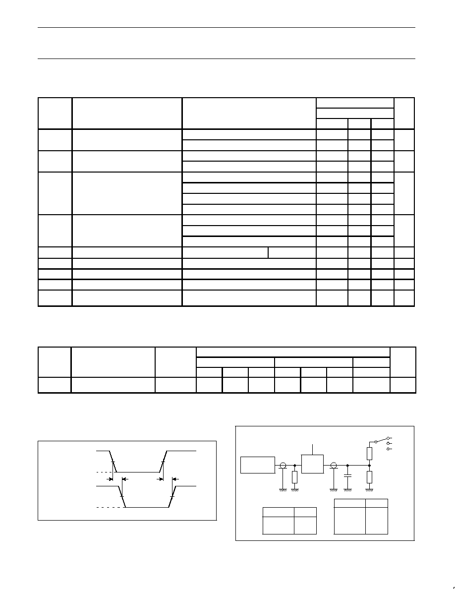
AC WAVEFORMS
V
M
= 1.5 V at V
CC
2.7 V; V
M
= 0.5 at V
CC
< 2.7 V; V
OL
and V
OH
are the typical output voltage drop that occur with the output load.
SV00477
VM
nA, nB INPUT
nY OUTPUT
VM
t PLH
t PHL
GND
V I
VOL
VOH
Figure 1.
Input (nA, nB) to output (nY) propagation delays
TEST CIRCUIT
PULSE
GENERATOR
V
I
R
T
D.U.T.
V
O
C
L
50pF
S
1
2
<
V
CC
Open
GND
500
500
V
CC
V
I
t
2.7V
V
CC
2.7V 3.6V
2.7V
Test
S
1
GND
t
PLZ
/t
PZL
2
<
V
CC
t
PHZ
/t
PZH
t
PLH
/t
PHL
Open
SY00003
V
CC
Figure 2.
Load circuitry for switching times.
Philips Semiconductors
Product specification
74LVC86
Quad 2-input EXCLUSIVE-OR gate
1997 Mar 18
5
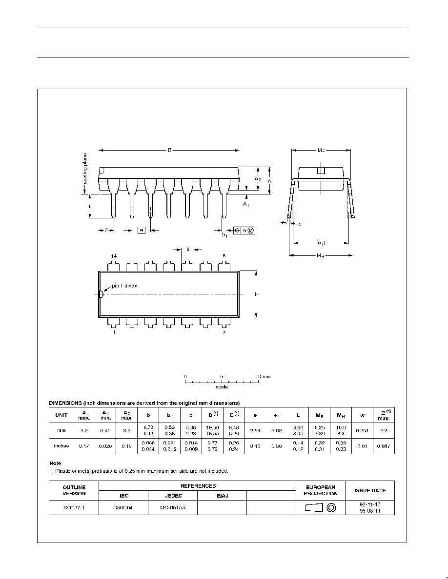
DIP14:
plastic dual in-line package; 14 leads (300 mil)
SOT27-1
Document Outline
- FEATURES
- DESCRIPTION
- QUICK REFERENCE DATA
- ORDERING INFORMATION
- PIN CONFIGURATION
- LOGIC SYMBOL (IEEE/IEC)
- PIN DESCRIPTION
- LOGIC SYMBOL
- FUNCTION TABLE
- LOGIC DIAGRAM (ONE GATE)
- RECOMMENDED OPERATING CONDITIONS
- ABSOLUTE MAXIMUM RATINGS
- DC ELECTRICAL CHARACTERISTICS
- AC CHARACTERISTICS
- AC WAVEFORMS
- TEST CIRCUIT
- PACKAGE OUTLINES
- SOT27-1
- SOT108-1
- SOT337-1
- SOT402-1
- DEFINITIONS