DATA SHEET
Product specification
File under Integrated Circuits, IC24
1999 Aug 05
INTEGRATED CIRCUITS
74LVC162374A; 74LVCH162374A
16-bit edge triggered D-type
flip-flop with 30
series termination
resistors; 5 V input/output tolerant;
3-state
1999 Aug 05
2
Philips Semiconductors
Product specification
16-bit edge triggered D-type flip-flop with 30
series
termination resistors; 5 V input/output tolerant; 3-state
74LVC162374A;
74LVCH162374A
FEATURES
∑
ESD protection:
HBM EIA/JESD22-A114-A
exceeds 2000 V
MM EIA/JESD22-A115-A
exceeds 200 V
∑
5 V tolerant input/output for
interfacing with 5 V logic
∑
Wide supply voltage range of
1.2 to 3.6 V
∑
Complies with JEDEC standard
no. 8-1A
∑
CMOS low power consumption
∑
MULTIBYTE
TM
flow-through
standard pin-out architecture
∑
Low inductance multiple power and
ground pins for minimum noise and
ground bounce
∑
Direct interface with TTL levels
∑
All data inputs have bus hold
(74LVCH162374A only)
∑
High impedance when V
CC
= 0
∑
Power off disables outputs,
permitting live insertion.
DESCRIPTION
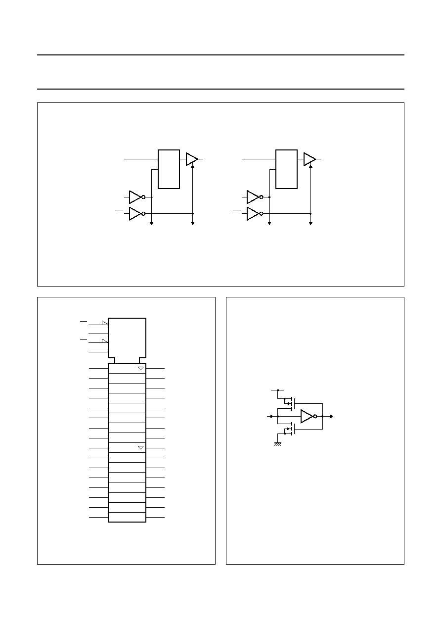
The 74LVC(H)162374A is a 16-bit edge triggered flip-flop featuring separate
D-type inputs for each flip-flop and 3-state outputs for bus oriented applications.
The 74LVC162374A consists of 2 sections of eight edge-triggered flip-flops.
A clock (CP) input and an output enable (OE) are provided for each octal.
Inputs can be driven from either 3.3 or 5 V devices. In 3-state operation,
outputs can handle 5 V. These features allow the use of these devices in a
mixed 3.3 and 5 V environment.
The flip-flops will store the state of their individual D-inputs that meet the set-up
and hold time requirements on the LOW-to-HIGH CP transition.
When OE is LOW, the contents of the flip-flops are available at the outputs.
When OE is HIGH, the outputs go to the high-impedance OFF-state.
Operation of the OE input does not affect the state of the flip-flops.
The 74LVCH162374A bus hold data inputs eliminates the need for external pull
up resistors to hold unused inputs.
The 74LVC(H)162374A is designed with 30
series termination resistors in
both HIGH and LOW output stages to reduce line noise.
FUNCTION TABLE
See note 1.
Note
1. H = HIGH voltage level;
h = HIGH voltage level one set-up time prior to the HIGH-to-LOW LE transition;
L = LOW voltage level;
l = LOW voltage level one set-up time prior to the HIGH-to-LOW LE transition;
Z = high-impedance OFF-state;
= LOW-to-HIGH CP transition.
OPERATION MODES
INPUTS
INTERNAL
FLIP-FLOPS
OUTPUTS
nOE
nCP
nD
n
Q
0
to Q
7
Load and read register
L
l
L
L
L
h
H
H
Latch register and disable outputs
H
l
L
Z
H
h
H
Z

1999 Aug 05
3
Philips Semiconductors
Product specification
16-bit edge triggered D-type flip-flop with 30
series
termination resistors; 5 V input/output tolerant; 3-state
74LVC162374A;
74LVCH162374A
QUICK REFERENCE DATA
GND = 0 V; T
amb
= 25
∞
C; t
r
= t
f
2.5 ns.
Note
1. C
PD
is used to determine the dynamic power dissipation (P
D
in
µ
W).
P
D
= C
PD
◊
V
CC
2
◊
f
i
+
(C
L
◊
V
CC
2
◊
f
o
) where:
f
i
= input frequency in MHz;
f
o
= output frequency in MHz;
(C
L
◊
V
CC
2
◊
f
o
) = sum of outputs;
C
L
= output load capacitance in pF;
V
CC
= supply voltage in Volts.
ORDERING INFORMATION
PINNING
SYMBOL
PARAMETER
CONDITIONS
TYPICAL
UNIT
t
PHL
/t
PLH
propagation delay CP to Q
n
C
L
= 50 pF; V
CC
= 3.3 V
3.8
ns
f
max
maximum clock frequency
150
MHz
C
I
input capacitance
5.0
pF
C
PD
power dissipation capacitance per
flip-flop
V
CC
= 3.3 V; note 1
30
pF
OUTSIDE NORTH
AMERICA
NORTH AMERICA
PACKAGE
TEMPERATURE
RANGE
PINS
PACKAGE
MATERIAL
CODE
74LVC162374ADL
VC162374A DL
-
40 to +85
∞
C
48
SSOP
plastic
SOT370-1
74LVC162374ADGG
VC162374A DGG
48
TSSOP
plastic
SOT362-1
74LVCH162374ADL
VCH162374A DL
48
SSOP
plastic
SOT370-1
74LVCH162374ADGG
VCH162374A DGG
48
TSSOP
plastic
SOT362-1
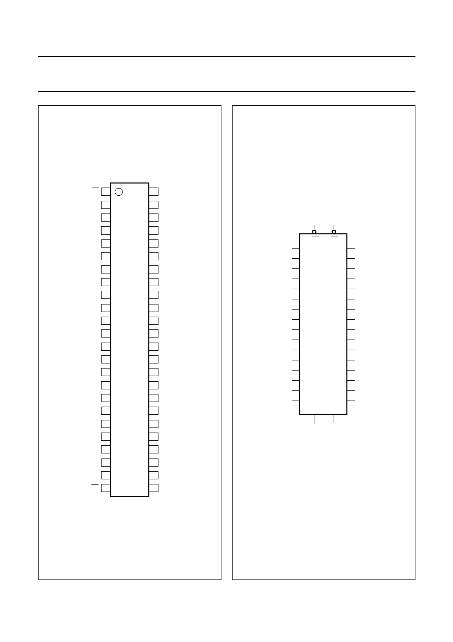
PIN
SYMBOL
DESCRIPTION
1
1OE
output enable input (active LOW)
2, 3, 5, 6, 8, 9, 11, 12
1Q
0
to 1Q
7
3-state flip-flop outputs
4, 10, 15, 21, 28, 34, 39, 45
GND
ground (0 V)
7, 18, 31, 42
V
CC
DC supply voltage
13, 14, 16, 17, 19, 20, 22, 23 2Q
0
to 2Q
7
3-state flip-flop outputs
24
2OE
output enable input (active LOW)
25
2CP
clock input
36, 35, 33, 32, 30, 29, 27, 26 2D
0
to 2D
7
data inputs
47, 46, 44, 43, 41, 40, 38, 37 1D
0
to 1D
7
data inputs
48
1CP
clock input
1999 Aug 05
4
Philips Semiconductors
Product specification
16-bit edge triggered D-type flip-flop with 30
series
termination resistors; 5 V input/output tolerant; 3-state
74LVC162374A;
74LVCH162374A
Fig.1 Pin configuration.
handbook, halfpage
162374A
MNA433
1
2
3
4
5
6
7
8
9
10
11
12
13
14
15
16
17
18
19
20
21
22
23
24
26
25
48
47
46
45
44
43
42
41
40
39
38
37
36
35
34
33
32
31
30
29
28
27
1Q0
1Q1
GND
1Q2
1Q3
VCC
1Q4
1Q5
GND
1Q6
1Q7
2Q0
2Q1
GND
2Q2
2Q3
VCC
2Q4
2Q5
GND
2Q6
2Q7
2OE
1D0
1D1
GND
1D2
1D3
VCC
1D4
1D5
GND
1D6
1D7
2D0
2D1
GND
2D2
2D3
VCC
2D4
2D5
GND
2D6
2D7
2CP
1OE
1CP
Fig.2 Logic symbol.
handbook, halfpage
MNA434
1Q0
1Q1
1CP
2CP
1Q2
1Q3
1Q4
1Q5
1Q6
1Q7
1OE
47
46
48
25
44
43
41
40
38
37
2
3
1
5
6
8
9
11
12
24
2Q0
2Q1
2Q2
2Q3
2Q4
2Q5
2Q6
2Q7
1D0
1D1
1D2
1D3
1D4
1D5
1D6
1D7
2D0
2D1
2D2
2D3
2D4
2D5
2D6
2D7
36
35
33
32
30
29
27
26
13
14
16
17
19
20
22
23
2OE
1999 Aug 05
5
Philips Semiconductors
Product specification
16-bit edge triggered D-type flip-flop with 30
series
termination resistors; 5 V input/output tolerant; 3-state
74LVC162374A;
74LVCH162374A
Fig.3 Logic diagram.
handbook, full pagewidth
MNA435
2CP
D
CP
Q
2OE
to 7 other channels
FF2
2Q0
2D0
1CP
D
CP
Q
1OE
to 7 other channels
FF1
1Q0
1D0
Fig.4 IEC logic symbol.
handbook, halfpage
23
MNA436
37
12
11
9
8
6
5
47
46
44
43
41
40
38
1D7
1D0
1D1
1D2
1D3
1D4
1D5
1D6
2
3
1Q7
1Q6
1Q5
1Q4
1Q3
1Q2
1Q0
1Q1
26
22
20
19
17
16
36
35
33
32
30
29
27
2D5
2D0
2D1
2D2
2D3
2D4
13
14
2Q5
2Q4
2Q3
2Q2
2Q1
2Q0
24
25
2EN
1OE
1
1EN
1CP
2OE
2CP
48
C3
C2
1D
1
2D
2
2D7
2D6
2Q7
2Q6
Fig.5 Bus hold circuit.
handbook, halfpage
to internal circuit
MNA428
VCC
input