1999 Nov 24
2
Philips Semiconductors
Product specification
32-bit transparent D-type latch with
5 V tolerant inputs/outputs; 3-state
74LVCH32373A
FEATURES
∑
5 V tolerant inputs/outputs for interfacing with 5 V logic
∑
Wide supply voltage range from 1.2 to 3.6 V
∑
CMOS low power consumption
∑
MULTIBYTE
TM
flow-trough standard pin-out architecture
∑
Low inductance multiple power and ground pins for
minimum noise and ground bounce
∑
Direct interface with TTL levels
∑
Bus hold on data inputs
∑
Typical output ground bounce voltage:
V
OLP
< 0.8 V at V
CC
= 3.3 V and T
amb
= 25
∞
C
∑
Typical output undershoot voltage:
V
OHV
> 2 V at V
CC
= 3.3 V and T
amb
= 25
∞
C
∑
Power off disables outputs, permitting live insertion
∑
Packaged in plastic fine-pitch ball grid array package.
DESCRIPTION
The 74LVCH32373A is a high-performance, low-power,
low-voltage, Si-gate CMOS device, superior to most
advanced CMOS compatible TTL families.
The inputs can be driven from either 3.3 or 5 V devices.
In 3-state operation, outputs can handle 5 V. These
features allow the use of these devices in a mixed
3.3 or 5 V environment.
The 74LVCH32373A is a 32-bit transparent D-type latch
featuring separate D-type inputs for each latch and 3-state
outputs for bus oriented applications. One latch enable
(nLE) input and one output enable (nOE) are provided for
each octal. Inputs can be driven from either 3.3 or 5 V
devices.
The 74LVCH32373A consists of 4 sections of eight D-type
transparent latches with 3-state true outputs. When input
nLE is HIGH, data at the nD
n
inputs enter the latches. In
this condition the latches are transparent, i.e. a latch
output will change each time its corresponding D-input
changes.
When input nLE is LOW the latches store the information
that was present at the D-inputs one set-up time preceding
the HIGH-to-LOW transition of nLE. When input nOE is
LOW, the contents of the eight latches are available at the
outputs. When input nOE is HIGH, the outputs go to the
high-impedance OFF-state. Operation of the nOE input
does not affect the state of the latches.
The 74LVCH32373A bus hold data input circuits eliminate
the need for external pull-up resistors to hold unused
inputs.
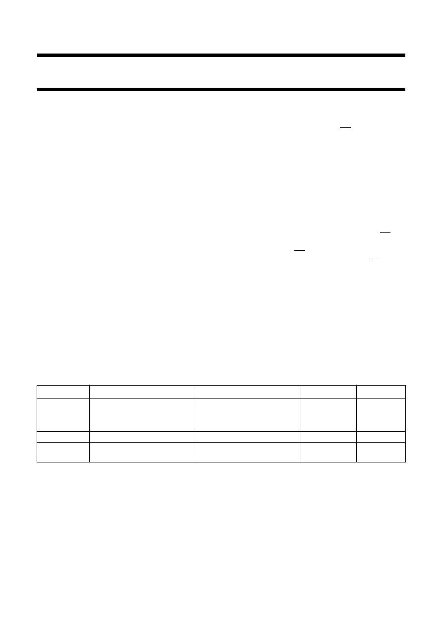
QUICK REFERENCE DATA
GND = 0 V; T
amb
= 25
∞
C; t
r
= t
f
2.5 ns.
Note
1. C
PD
is used to determine the dynamic power dissipation (P
D
in
µ
W).
P
D
= C
PD
◊
V
CC
2
◊
f
i
+
(C
L
◊
V
CC
2
◊
f
o
) where:
f
i
= input frequency in MHz;
f
o
= output frequency in MHz;
C
L
= output load capacitance in pF;
V
CC
= supply voltage in Volts;
(C
L
◊
V
CC
2
◊
f
o
) = sum of the outputs.
SYMBOL
PARAMETER
CONDITIONS
TYPICAL
UNIT
t
PHL
/t
PLH
propagation delay
nD
n
to nQ
n
C
L
= 50 pF; V
CC
= 3.3 V
3.0
ns
nLE to nQ
n
C
L
= 50 pF; V
CC
= 3.3 V
3.4
ns
C
I
input capacitance
5.0
pF
C
PD
power dissipation capacitance
per buffer
V
I
= GND to V
CC
; note 1
26
pF
1999 Nov 24
3
Philips Semiconductors
Product specification
32-bit transparent D-type latch with
5 V tolerant inputs/outputs; 3-state
74LVCH32373A
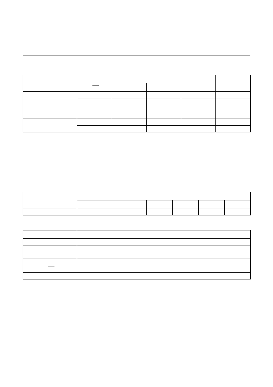
FUNCTION TABLE
See note 1.
Note
1. H = HIGH voltage level;
h = HIGH voltage level one set-up time prior to the HIGH-to-LOW LE transition;
L = LOW voltage level;
l = LOW voltage level one set-up time prior to the HIGH-to-LOW LE transition;
Z = high-impedance OFF-state.
ORDERING INFORMATION
PINNING
OPERATING MODE
INPUTS
INTERNAL
LATCHES
OUTPUTS
nOE
nLE
nD
n
nQ
n
Enable and read register
(transparent mode)
L
H
L
L
L
L
H
H
H
H
Latch and read register
L
L
l
L
L
L
L
h
H
H
Latch register and disable
outputs
H
L
l
L
Z
H
L
h
H
Z
TYPE NUMBER
PACKAGE
TEMPERATURE RANGE
PINS
PACKAGE
MATERIAL
CODE
74LVCH32373AEC
-
40 to +85
∞
C
96
LFBGA96
plastic
SOT536-1
SYMBOL
DESCRIPTION
nD
n
data inputs
nLE
latch enable inputs (active HIGH)
nQ
n
data outputs
GND
ground (0 V)
nOE
output enable inputs (active LOW)
V
CC
DC supply voltage
1999 Nov 24
4
Philips Semiconductors
Product specification
32-bit transparent D-type latch with
5 V tolerant inputs/outputs; 3-state
74LVCH32373A
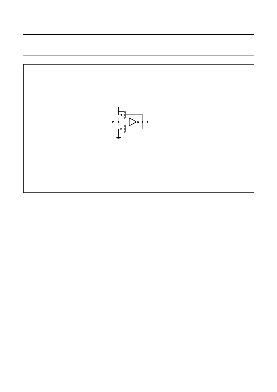
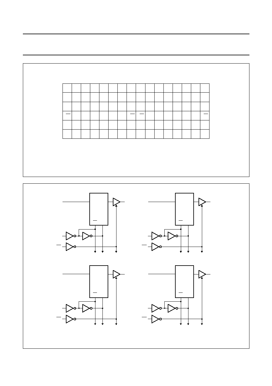
handbook, full pagewidth
MNA492
1D1 1D3 1D5 1D7 2D1 2D3 2D5 2D7 3D1 3D3 3D5 3D7 4D1 4D3 4D5 4D6
1D0 1D2 1D4 1D6 2D0 2D2 2D4 2D6 3D0 3D2 3D4 3D6 4D0 4D2 4D4 4D7
1Q0 1Q2 1Q4 1Q6 2Q0 2Q2 2Q4 2Q6 3Q0 3Q2 3Q4 3Q6 4Q0 4Q2 4Q4 4Q7
1Q1 1Q3 1Q5 1Q7 2Q1 2Q3 2Q5 2Q7 3Q1 3Q3 3Q5 3Q7 4Q1 4Q3 4Q5 4Q6
1LE
2LE
3LE
GND
GND GND
GND
4LE
VCC
VCC
GND
GND GND
GND
VCC
VCC
1OE
6
5
2
1
4
3
2OE 3OE
GND
GND GND
GND
4OE
VCC
VCC
GND
GND GND
GND
VCC
VCC
A
H
J
B
D
E
G
T
C
F
K
M
N
R
L
P
Fig.1 Pin configuration.
handbook, full pagewidth
MNA493
LE
LE
1Q0
LATCH 1
to 7 other channels
D
Q
1OE
1D0
1LE
LE
LE
2Q0
LATCH 9
to 7 other channels
D
Q
2OE
2D0
2LE
LE
LE
3Q0
LATCH 17
to 7 other channels
D
Q
3OE
3D0
3LE
LE
LE
4Q0
LATCH 25
to 7 other channels
D
Q
4OE
4D0
4LE
Fig.2 Logic symbol.
Fig.2 Logic symbol.