Philips Semiconductors
Product specification
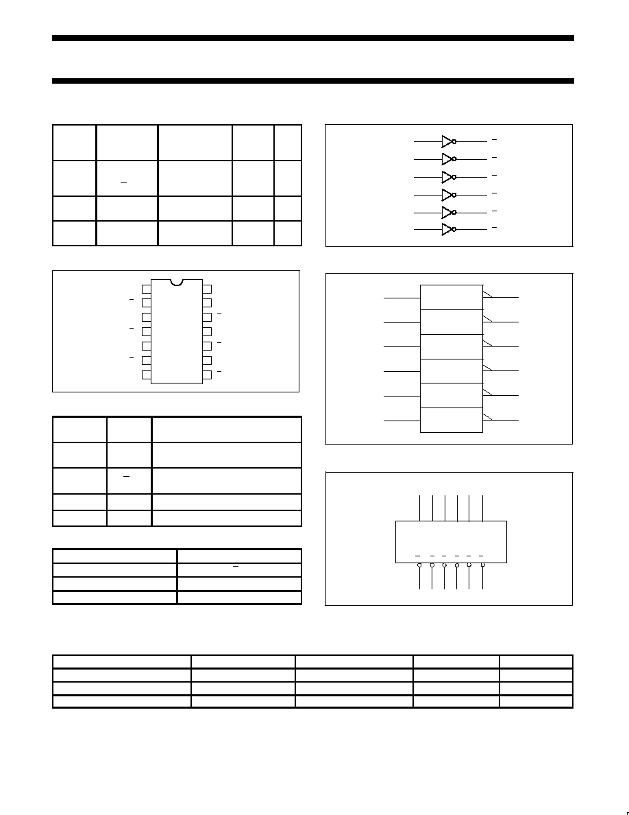
74LVT04
3.3V Hex inverter
1996 Aug 28
3
ABSOLUTE MAXIMUM RATINGS
1, 2
SYMBOL
PARAMETER
CONDITIONS
RATING
UNIT
V
CC
DC supply voltage
0.5 to +4.6
V
I
IK
DC input diode current
V
I
< 0
50
mA
V
I
DC input voltage
3
0.5 to +7.0
V
I
OK
DC output diode current
V
O
< 0
50
mA
V
OUT
DC output voltage
3
Output in Off or High state
0.5 to +7.0
V
I
O
DC output current
Output in High state
32
mA
I
OUT
DC output current
Output in Low state
64
mA
T
stg
Storage temperature range
65 to 150
°
C
NOTES:
1. Stresses beyond those listed may cause permanent damage to the device. These are stress ratings only and functional operation of the
device at these or any other conditions beyond those indicated under "recommended operating conditions" is not implied. Exposure to
absolute-maximum-rated conditions for extended periods may affect device reliability.
2. The performance capability of a high-performance integrated circuit in conjunction with its thermal environment can create junction
temperatures which are detrimental to reliability. The maximum junction temperature of this integrated circuit should not exceed 150
°
C.
3. The input and output negative voltage ratings may be exceeded if the input and output clamp current ratings are observed.
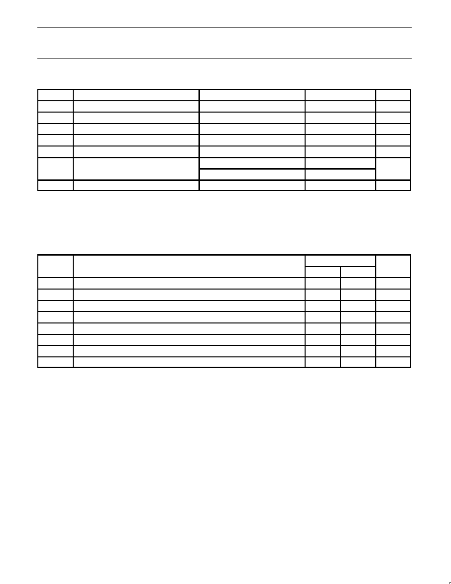
RECOMMENDED OPERATING CONDITIONS
SYMBOL
PARAMETER
LIMITS
UNIT
SYMBOL
PARAMETER
MIN
MAX
UNIT
V
CC
DC supply voltage
2.7
3.6
V
V
I
Input voltage
0
5.5
V
V
IH
High-level input voltage
2.0
V
V
IL
Low-level Input voltage
0.8
V
I
OH
High-level output current
20
mA
I
OL
Low-level output current
32
mA
t/
v
Input transition rise or fall rate; Outputs enabled
10
ns/V
T
amb
Operating free-air temperature range
40
+85
°
C
Philips Semiconductors
Product specification
74LVT04
3.3V Hex inverter
1996 Aug 28
4
DC ELECTRICAL CHARACTERISTICS
Over recommended operating conditions
Voltages are referenced to GND (ground = 0V)
LIMITS
SYMBOL
PARAMETER
TEST CONDITIONS
Temp = -40
°
C to +85
°
C
UNIT
MIN
TYP
1
MAX
V
IK
Input clamp voltage
V
CC
= 2.7V; I
IK
= 18mA
1.2
V
V
CC
= 2.7 to 3.6V; I
OH
= 100
µ
A
V
CC
0.2
V
OH
High-level output voltage
V
CC
= 2.7V; I
OH
= 6mA
2.4
V
V
CC
= 3.0V; I
OH
= 20mA
2.0
V
CC
= 2.7V; I
OL
= 100
µ
A
0.2
V
OL
Lowlevel output voltage
V
CC
= 2.7V; I
OL
= 24mA
0.5
V
V
CC
= 3.0V; I
OL
= 32mA
0.5
I
Input leakage current
V
CC
= 0 or 3.6V; V
I
= 5.5V
10
A
I
I
Input leakage current
V
CC
= 3.6V; V
I
= V
CC
or GND
±
1
µ
A
I
OFF
Output off current
V
CC
= 0V; V
I
or V
O
= 0 to 4.5V
±
100
µ
A
I
CCH
Quiescent supply current
V
CC
= 3.6V; Outputs High, V
I
= GND or
V
CC,
I
O =
0
0.02
mA
I
CCL
Quiescent supply current
V
CC
= 3.6V; Outputs Low, V
I
= GND or V
CC,
I
O =
0
1.5
3
mA
I
CC
Additional supply current per input pin
2
V
CC
= 3V to 3.6V; One input at V
CC
0.6V,
Other inputs at V
CC
or GND
0.2
µ
A
C
I
Input capacitance
V
I
= 3V or 0
3
pF
NOTES:
1. All typical values are at V
CC
= 3.3V and T
amb
= 25
°
C.
2. This is the increase in supply current for each input at the specificed voltage level other than V
CC
or GND.
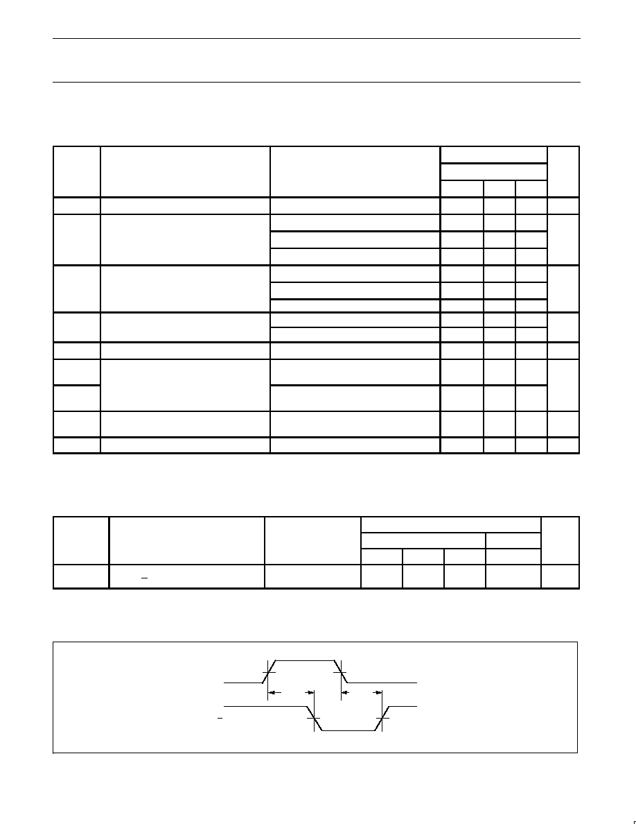
AC CHARACTERISTICS
GND = 0V; t
R
= t
F
= 2.5ns; C
L
= 50pF, R
L
= 500
; T
amb
= 40
°
C to +85
°
C.
LIMITS
SYMBOL
PARAMETER
WAVEFORM
V
CC
= 3.3V
±
0.3V
V
CC
= 2.7V
UNIT
MIN
TYP
1
MAX
MAX
t
PLH
t
PHL
Propagation delay
An to Yn
1
1.0
1.0
2.6
2.5
3.9
3.5
4.7
3.2
ns
NOTE:
1. All typical values are at V
CC
= 3.3V and T
amb
= 25
°
C.
AC WAVEFORMS
V
M
= 1.5V, V
IN
= GND to 2.7V
VM
VM
VM
VM
Y
A
tPHL
tPLH
SF00015
Waveform 1.
Propagation delay for inverting outputs
Philips Semiconductors
Product specification
74LVT04
3.3V Hex inverter
1996 Aug 28
5
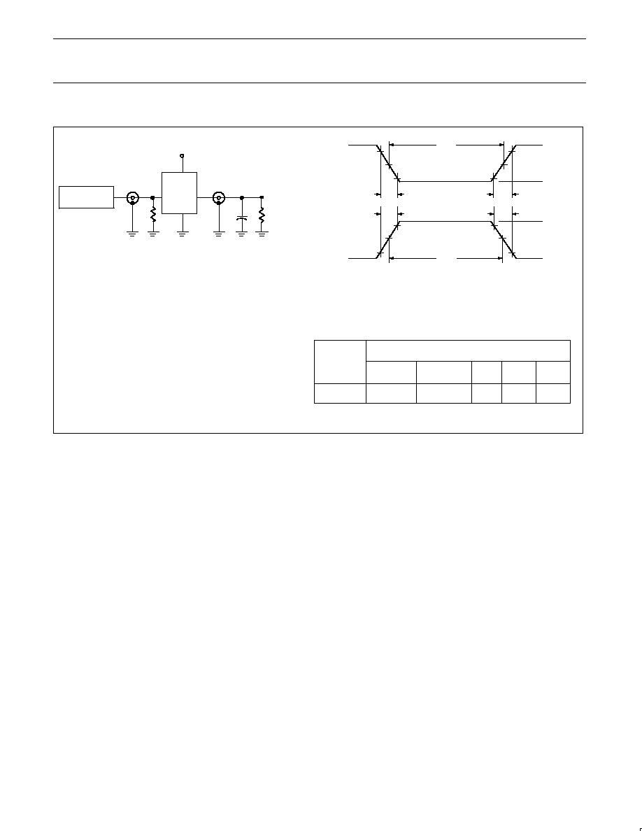
TEST CIRCUIT AND WAVEFORMS
VM
VM
tW
AMP (V)
NEGATIVE
PULSE
10%
10%
90%
90%
0V
VM
VM
tW
AMP (V)
POSITIVE
PULSE
90%
90%
10%
10%
0V
tTHL (tF)
tTLH (tR)
tTHL (tF)
tTLH (tR)
V
M
= 1.5V
Input Pulse Definition
DEFINITIONS
R
L
=
Load resistor; see AC CHARACTERISTICS for value.
C
L
=
Load capacitance includes jig and probe capacitance;
see AC CHARACTERISTICS for value.
R
T
=
Termination resistance should be equal to Z
OUT
of
pulse generators.
INPUT PULSE REQUIREMENTS
FAMILY
Amplitude
Rep. Rate
t
W
t
R
t
F
74LVT
2.7V
10MHz
500ns
2.5ns
2.5ns
PULSE
GENERATOR
VIN
D.U.T.
VOUT
CL
VCC
Test Circuit for Outputs
R
T
RL
SV00022