Äîêóìåíòàöèÿ è îïèñàíèÿ www.docs.chipfind.ru

1.
General description
The LVT125 is a high-performance BiCMOS product designed for V
CC
operation at 3.3 V.
This device combines low static and dynamic power dissipation with high speed and high
output drive. The 74LVT125 device is a quad buffer that is ideal for driving bus lines. The
device features four output enable inputs (1OE, 2OE, 3OE and 4OE), each controlling one
of the 3-state outputs.
2.
Features
s
Quad bus interface
s
3-state buffers
s
Output capability: +64 mA and
-
32 mA
s
TTL input and output switching levels
s
Input and output interface capability to systems at 5 V supply
s
Bus-hold data inputs eliminate the need for external pull-up resistors to hold unused
inputs
s
Live insertion and extraction permitted
s
No bus current loading when output is tied to 5 V bus
s
Power-up 3-state
s
Latch-up protection:
x
JESD78: exceeds 500 mA
s
ESD protection:
x
MIL STD 883 method 3015: exceeds 2000 V
x
Machine model: exceeds 200 V
3.
Quick reference data
74LVT125
3.3 V quad buffer; 3-state
Rev. 05 -- 10 February 2005
Product data sheet
Table 1:
Quick reference data
GND = 0 V; T
amb
= 25
°
C.
Symbol Parameter
Conditions
Min
Typ
Max
Unit
t
PLH
propagation delay nA to nY C
L
= 50 pF; V
CC
= 3.3 V
-
2.7
-
ns
t
PHL
propagation delay nA to nY C
L
= 50 pF; V
CC
= 3.3 V
-
2.9
-
ns
C
I
input capacitance
V
I
= 0 V or 3.0 V
-
4
-
pF
C
O
output capacitance
outputs disabled;
V
O
= 0 V or 3.0 V
-
8
-
pF
I
CC
quiescent supply current
outputs disabled;
V
CC
= 3.6 V
-
0.13
-
mA
9397 750 14703
© Koninklijke Philips Electronics N.V. 2005. All rights reserved.
Product data sheet
Rev. 05 -- 10 February 2005
2 of 15
Philips Semiconductors
74LVT125
3.3 V quad buffer; 3-state
4.
Ordering information
5.
Functional diagram
Table 2:
Ordering information
Type number
Package
Temperature range
Name
Description
Version
74LVT125D
-
40
°
C to +85
°
C
SO14
plastic small outline package; 14 leads;
body width 3.9 mm
SOT108-1
74LVT125DB
-
40
°
C to +85
°
C
SSOP14
plastic shrink small outline package; 14 leads;
body width 5.3 mm
SOT337-1
74LVT125PW
-
40
°
C to +85
°
C
TSSOP14
plastic thin shrink small outline package; 14 leads;
body width 4.4 mm
SOT402-1
74LVT125BQ
-
40
°
C to +85
°
C
DHVQFN14 plastic dual in-line compatible thermal enhanced very thin
quad flat package; no leads; 14 leads terminals;
body 2.5
×
3
×
0.85 mm
SOT762-1
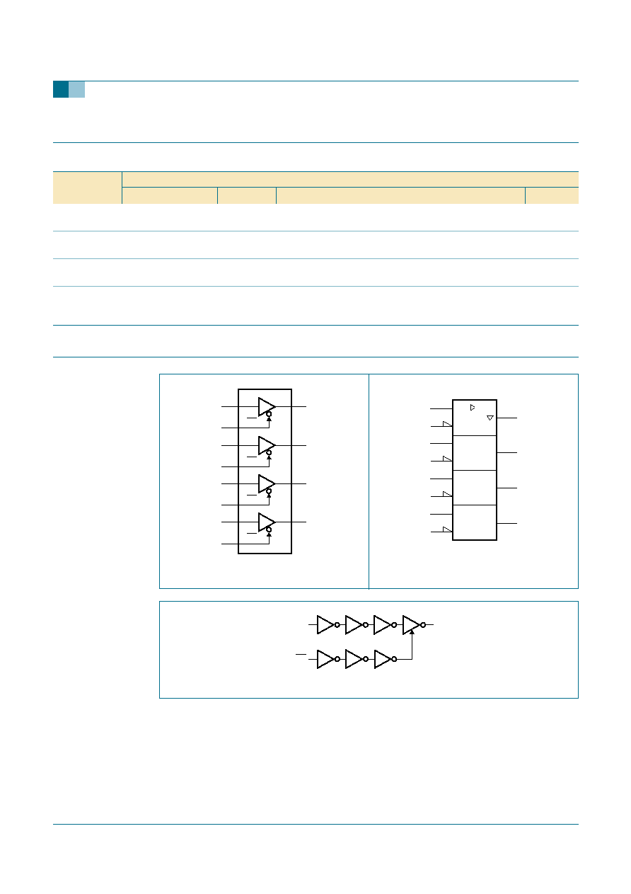
Fig 1.
Logic symbol
Fig 2.
IEC logic symbol
Fig 3.
Logic diagram
mna228
1A
1Y
2
1
3
1OE
2A
2Y
5
4
6
2OE
3A
3Y
9
10
8
3OE
4A
4Y
12
13
11
4OE
mna229
1
EN1
1
3
2
4
6
5
10
8
9
13
11
12
mna227
nOE
nA
nY

9397 750 14703
© Koninklijke Philips Electronics N.V. 2005. All rights reserved.
Product data sheet
Rev. 05 -- 10 February 2005
3 of 15
Philips Semiconductors
74LVT125
3.3 V quad buffer; 3-state
6.
Pinning information
6.1 Pinning
6.2 Pin description
(1) The die substrate is attached to the
exposed die pad using conductive die
attach material. It can not be used as
a supply pin or input.
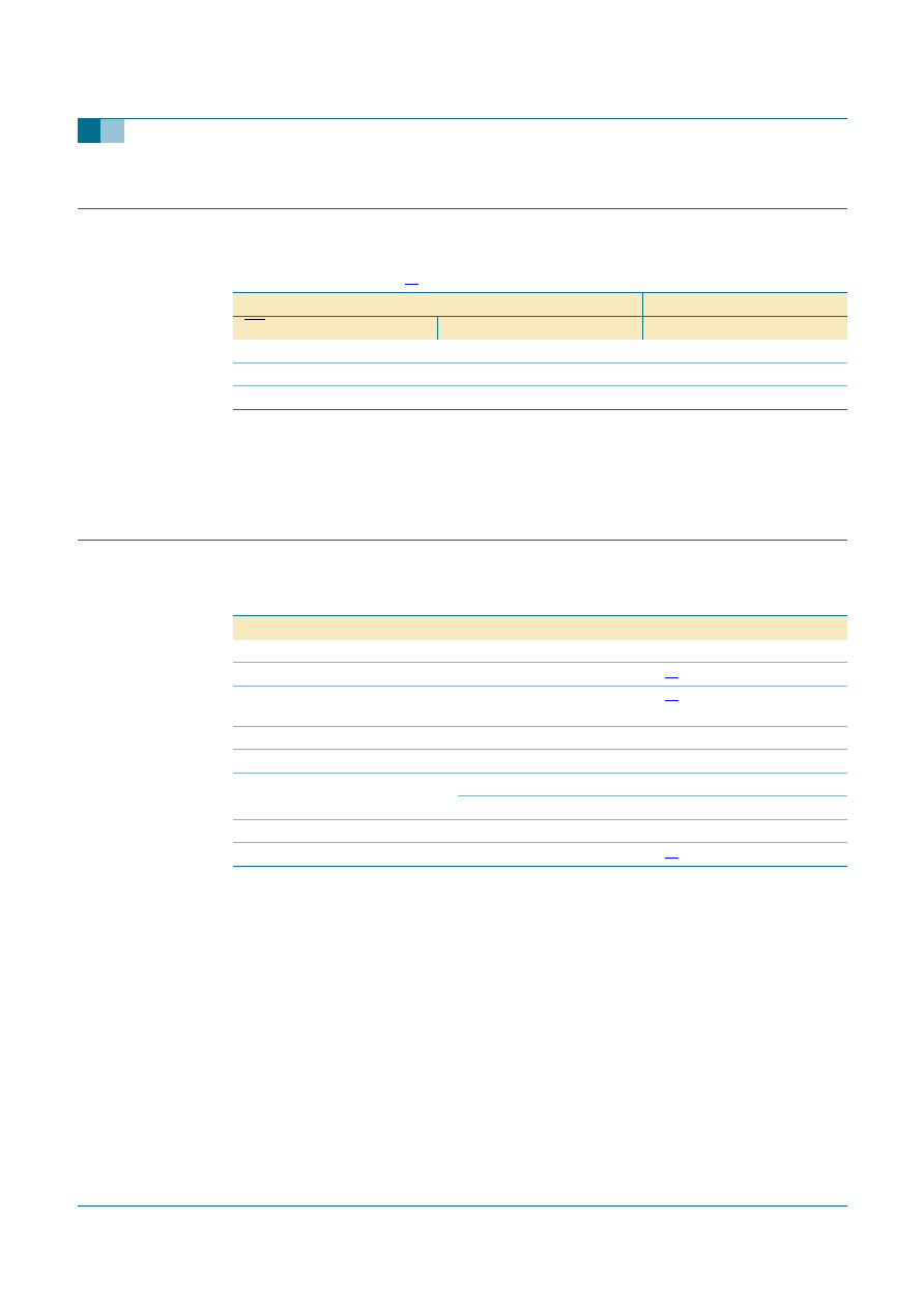
Fig 4.
Pin configuration SO14, SSOP14
and TSSOP14
Fig 5.
Pin configuration DHVQFN14
125
1OE
V
CC
1A
4OE
1Y
4A
2OE
4Y
2A
3OE
2Y
3A
GND
3Y
001aac476
1
2
3
4
5
6
7
8
10
9
12
11
14
13
001aac477
125
Transparent top view
2Y
3A
2A
3OE
2OE
4Y
1Y
4A
1A
4OE
GND
3Y
1OE
V
CC
6
9
5
10
4
11
3
12
2
13
7
8
1
14
terminal 1
index area
GND
(1)
Table 3:
Pin description
Symbol
Pin
Description
1OE
1
1 output enable input (active LOW)
1A
2
1 data input
1Y
3
1 data output
2OE
4
2 output enable input (active LOW)
2A
5
2 data input
2Y
6
2 data output
GND
7
ground (0 V)
3Y
8
3 data output
3A
9
3 data input
3OE
10
3 output enable input (active LOW)
4Y
11
4 data output
4A
12
4 data input
4OE
13
4 output enable input (active LOW)
V
CC
14
supply voltage
9397 750 14703
© Koninklijke Philips Electronics N.V. 2005. All rights reserved.
Product data sheet
Rev. 05 -- 10 February 2005
4 of 15
Philips Semiconductors
74LVT125
3.3 V quad buffer; 3-state
7.
Functional description
7.1 Function table
[1]
H = HIGH voltage level;
L = LOW voltage level;
X = don't care;
Z = high-impedance OFF-state.
8.
Limiting values
[1]
The input and output negative voltage ratings may be exceeded if the input and output clamp current ratings
are observed.
[2]
The performance capability of a high-performance integrated circuit in conjunction with its thermal
environment can create junction temperatures which are detrimental to reliability.
Table 4:
Function table
[1]
Input
Output
nOE
nA
nY
L
L
L
L
H
H
H
X
Z
Table 5:
Limiting values
In accordance with the Absolute Maximum Rating System (IEC 60134). Voltages are referenced to
GND (ground = 0 V).
Symbol Parameter
Conditions
Min
Max
Unit
V
CC
supply voltage
-
0.5
+4.6
V
V
I
input voltage
[1]
-
0.5
+7.0
V
V
O
output voltage
output in OFF-state or
HIGH-state
[1]
-
0.5
+7.0
V
I
IK
input diode current
V
I
< 0 V
-
-
50
mA
I
OK
output diode current
V
O
< 0 V
-
-
50
mA
I
O
output current
output in LOW-state
-
128
mA
output in HIGH-state
-
-
64
mA
T
stg
storage temperature
-
65
+150
°
C
T
j
junction temperature
[2]
-
150
°
C

9397 750 14703
© Koninklijke Philips Electronics N.V. 2005. All rights reserved.
Product data sheet
Rev. 05 -- 10 February 2005
5 of 15
Philips Semiconductors
74LVT125
3.3 V quad buffer; 3-state
9.
Recommended operating conditions
10. Static characteristics
Table 6:
Recommended operating conditions
Symbol Parameter
Conditions
Min
Typ
Max
Unit
V
CC
supply voltage
2.7
-
3.6
V
V
I
input voltage
0
-
5.5
V
V
IH
HIGH-level input voltage
2.0
-
-
V
V
IL
LOW-level input voltage
-
-
0.8
V
I
OH
HIGH-level output current
-
-
-
32
mA
I
OL
LOW-level output current
none
-
-
32
mA
current duty cycle
50 %; f
1 kHz
-
-
64
mA
t/
V
input transition rise or fall
rate
0
-
10
ns/V
T
amb
ambient temperature
in free air
-
40
-
+85
°
C
Table 7:
Static characteristics
At recommended operating conditions; voltages are referenced to GND (ground = 0 V).
Symbol Parameter
Conditions
Min
Typ
Max
Unit
T
amb
=
-
40
°
C to +85
°
C
[1]
V
IK
input diode voltage
I
IK
=
-
18 mA; V
CC
= 2.7 V
-
-
0.9
-
1.2
V
V
OH
HIGH-level output voltage
I
OH
=
-
100
µ
A;
V
CC
= 2.7 V to 3.6 V;
V
CC
-
0.2 V
CC
-
0.1 -
V
I
OH
=
-
8 mA; V
CC
= 2.7 V
2.4
2.5
-
V
I
OH
=
-
32 mA; V
CC
= 3.0 V
2.0
2.2
-
V
V
OL
LOW-level output voltage
V
CC
= 2.7 V
I
OL
= 100
µ
A
-
0.1
0.2
V
I
OL
= 24 mA
-
0.3
0.5
V
V
CC
= 3.0 V
I
OL
= 16 mA
-
0.25
0.4
V
I
OL
= 32 mA
-
0.3
0.5
V
I
OL
= 64 mA
-
0.4
0.55
V
I
LI
input leakage current
all input pins
V
CC
= 0 V or 3.6 V; V
I
= 5.5 V
-
1
10
µ
A
control pins
V
CC
= 3.6 V; V
CC
or GND
-
±
0.1
±
1
µ
A
data pins
V
CC
= 3.6 V; V
I
= V
CC
[2]
-
0.1
1
µ
A
V
CC
= 3.6 V; V
I
= 0 V
[2]
-
-
1
-
5
µ
A
I
OFF
power-down output current
V
CC
= 0 V; V
I
or V
O
= 0 V to 4.5 V
-
1
±
100
µ
A
I
HOLD
bus hold current nA input
V
CC
= 3 V; V
I
= 0.8 V
[3]
75
150
-
µ
A
V
CC
= 3 V; V
I
= 2.0 V
-
75
-
150
-
µ
A
V
CC
= 0 V to 3.6 V; V
I
= 3.6 V
±
500
-
-
µ
A
Document Outline