
Philips
Semiconductors
74LVT14
3.3V Hex inverter Schmitt trigger
Product specification
1996 Aug 28
INTEGRATED CIRCUITS
IC24 Data Handbook

Philips Semiconductors
Product specification
74LVT14
3.3V Hex inverter Schmitt trigger
2
1996 Aug 28
853-1870 17244
DESCRIPTION
The 74LVT14 is a high-performance BiCMOS product designed for
V
CC
operation at 3.3V. They are capable of transforming slowly
changing input signals into sharply defined, jitter free output signals.
In addition, they have greater noise margin than conventional
inverters. Each circuit contains a Schmitt trigger followed by a
Darlington level shifter and a phase splitter driving a TTL totem-pole
output. The Schmitt trigger uses positive feedback to effectively
speed-up slow input transitions, and provide different input threshold
voltages for positive-going and negative-going input threshold
(typically 600mV) is determined internally by resistor ratios and is
insensitive to temperature and supply voltage variations.
QUICK REFERENCE DATA
SYMBOL
PARAMETER
CONDITIONS
T
amb
= 25
�
C;
GND = 0V
TYPICAL
UNIT
t
PLH
t
PHL
Propagation
delay
An to Yn
C
L
= 50pF;
V
CC
= 3.3V
3.2
3.0
ns
C
IN
Input
capacitance
V
I
= 0V or 3.0V
3
pF
I
CCL
Total supply
current
Outputs low;
V
CC
= 3.6V
1.5
mA
PIN CONFIGURATION
14
13
12
11
10
9
8
7
6
5
4
3
2
1
GND
V
CC
Y4
A3
Y3
A4
A5
Y5
A0
Y0
Y2
A1
Y1
A2
SA00338
PIN DESCRIPTION
PIN
NUMBER
SYMBOL
NAME AND FUNCTION
1, 3, 5, 9,
11, 13
An
Data inputs
2, 4, 6, 8,
10, 12
Yn
Data outputs
7
GND
Ground (0V)
14
V
CC
Positive supply voltage
FUNCTION TABLE
INPUTS
OUTPUT
Dn
Qn
L
H
H
L
NOTES:
H = High voltage level
L
= Low voltage level
LOGIC DIAGRAM
V
CC
= Pin 14
GND = Pin 7
SV00087
2
4
6
8
10
12
Y0
Y1
Y2
Y3
Y4
Y5
1
3
5
9
11
13
A0
A1
A2
A3
A4
A5
IEC/IEEE SYMBOL
13
1
SF00031
12
11
10
9
8
5
6
3
4
1
2
ORDERING INFORMATION
PACKAGES
TEMPERATURE RANGE
OUTSIDE NORTH AMERICA
NORTH AMERICA
DWG NUMBER
14-Pin Plastic SO
�40
�
C to +85
�
C
74LVT14 D
74LVT14 D
SOT108-1
14-Pin Plastic SSOP
�40
�
C to +85
�
C
74LVT14 DB
74LVT14 DB
SOT337-1
14-Pin Plastic TSSOP
�40
�
C to +85
�
C
74LVT14 PW
74LVT14 PWDH
SOT402-1

Philips Semiconductors
Product specification
74LVT14
3.3V Hex inverter Schmitt trigger
1996 Aug 28
3
LOGIC SYMBOL
4
6
8
10
1
3
5
9
11
13
V
CC
= Pin 14
GND = Pin 7
SV00088
A0
A1 A2 A3 A4 A5
2
Y0
Y1 Y2 Y3 Y4 Y5
12
ABSOLUTE MAXIMUM RATINGS
1, 2
SYMBOL
PARAMETER
CONDITIONS
RATING
UNIT
V
CC
DC supply voltage
�0.5 to +4.6
V
I
IK
DC input diode current
V
I
< 0
�50
mA
V
I
DC input voltage
3
�0.5 to +7.0
V
I
OK
DC output diode current
V
O
< 0
�50
mA
V
OUT
DC output voltage
3
Output in Off or High state
�0.5 to +7.0
V
I
OUT
DC output current
Output in High state
�32
mA
I
OUT
DC output current
Output in Low state
64
mA
T
stg
Storage temperature range
�65 to 150
�
C
NOTES:
1. Stresses beyond those listed may cause permanent damage to the device. These are stress ratings only and functional operation of the
device at these or any other conditions beyond those indicated under "recommended operating conditions" is not implied. Exposure to
absolute-maximum-rated conditions for extended periods may affect device reliability.
2. The performance capability of a high-performance integrated circuit in conjunction with its thermal environment can create junction
temperatures which are detrimental to reliability. The maximum junction temperature of this integrated circuit should not exceed 150
�
C.
3. The input and output negative voltage ratings may be exceeded if the input and output clamp current ratings are observed.
RECOMMENDED OPERATING CONDITIONS
SYMBOL
PARAMETER
LIMITS
UNIT
SYMBOL
PARAMETER
MIN
MAX
UNIT
V
CC
DC supply voltage
2.7
3.6
V
V
I
Input voltage
0
5.5
V
V
IH
High-level input voltage
2.0
V
V
IL
Low-level Input voltage
0.8
V
I
OH
High-level output current
�20
mA
I
OL
Low-level output current
32
mA
t/
v
Input transition rise or fall rate; Outputs enabled
10
ns/V
T
amb
Operating free-air temperature range
�40
+85
�
C
Philips Semiconductors
Product specification
74LVT14
3.3V Hex inverter Schmitt trigger
1996 Aug 28
4
DC ELECTRICAL CHARACTERISTICS
Over recommended operating conditions
Voltages are referenced to GND (ground = 0V)
PARAMETER
LIMITS
SYMBOL
PARAMETER
TEST CONDITIONS
Temp = -40
�
C to +85
�
C
UNIT
MIN
TYP
1
MAX
V
T+
Positive-going threshold
V
CC
= 3.3V
1.5
1.7
2.0
V
V
T�
Negative-going threshold
V
CC
= 3.3V
0.9
1.1
1.3
V
V
T
Hysteresis
V
CC
= 3.3V
0.4
0.6
V
V
IK
Input clamp voltage
V
CC
= 2.7V; I
IK
= �18mA
�1.2
V
V
OH
High-level output voltage
V
CC
= 2.7 to 3.6V; I
OH
= �100
�
A
V
CC
�0.2
V
V
OH
High-level output voltage
V
CC
= 2.7V; I
OH
= �6mA
2.4
V
V
CC
= 3.0V; I
OH
= �20mA
2.0
V
OL
Low�level output voltage
V
CC
= 2.7V; I
OL
= 100
�
A
0.2
V
V
OL
Low�level output voltage
V
CC
= 2.7V; I
OL
= 24mA
0.5
V
V
CC
= 3.0V; I
OL
= 32mA
0.5
I
I
Input leakage current
V
CC
= 0 or 3.6V; V
I
= 5.5V
10
�
A
I
I
Input leakage current
V
CC
= 3.6V; V
I
= V
CC
or GND
�
1
�
A
I
OFF
Output off current
V
CC
= 0V; V
I
or V
O
= 0 to 4.5V
�
100
�
A
I
CCH
Quiescent supply current
V
CC
= 3.6V; Outputs High, V
I
= GND or
V
CC,
I
O =
0
0.02
mA
I
CCL
Quiescent supply current
V
CC
= 3.6V; Outputs Low, V
I
= GND or V
CC,
I
O =
0
1.5
3
mA
I
CC
Additional supply current per input pin
2
V
CC
= 3V to 3.6V; One input at V
CC
�0.6V,
Other inputs at V
CC
or GND
0.2
�
A
C
I
Input capacitance
V
I
= 3V or 0
3
pF
NOTES:
1. All typical values are at V
CC
= 3.3V and T
amb
= 25
�
C.
2. This is the increase in supply current for each input at the specificed voltage level other than V
CC
or GND
AC ELECTRICAL CHARACTERISTICS
SYMBOL
PARAMETER
TEST
CONDITION
LIMITS
UNIT
SYMBOL
PARAMETER
TEST
CONDITION
V
CC
= 3.3V
�
0.3V
V
CC
= 2.7V
UNIT
CONDITION
MIN
TYP
MAX
MAX
t
PLH
t
PHL
Propagation delay
An to Yn
Waveform 1
1.0
1.0
3.8
3.2
5.7
4.5
6.9
4.1
ns
AC WAVEFORMS
V
M
= 1.5V, V
IN
= GND to 2.7V
VM
VM
VM
VM
Yn
An
tPHL
tPLH
SA00341
Waveform 1.
Propagation delay for inverting outputs

Philips Semiconductors
Product specification
74LVT14
3.3V Hex inverter Schmitt trigger
1996 Aug 28
5
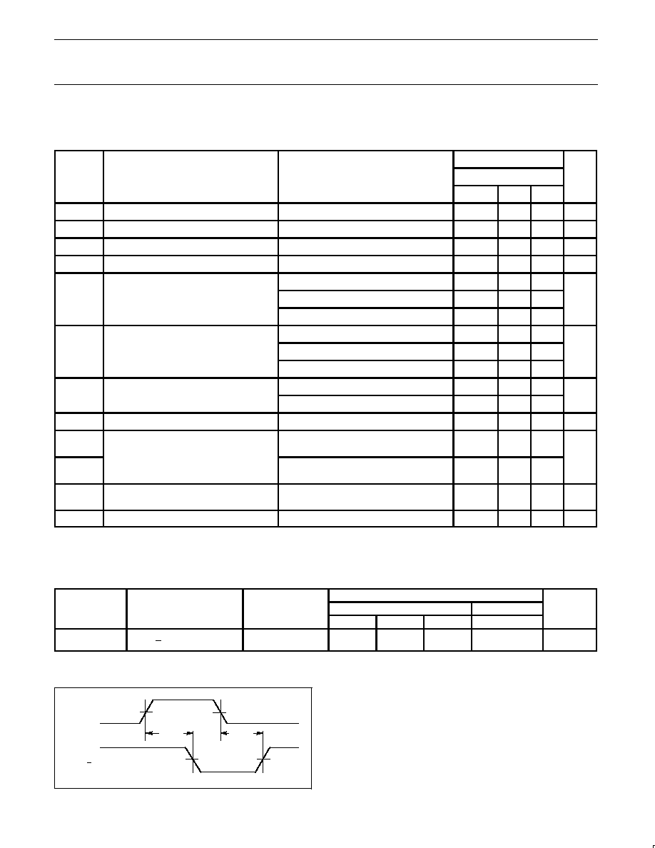
TEST CIRCUIT AND WAVEFORMS
VM
VM
tW
AMP (V)
NEGATIVE
PULSE
10%
10%
90%
90%
0V
VM
VM
tW
AMP (V)
POSITIVE
PULSE
90%
90%
10%
10%
0V
tTHL (tF)
tTLH (tR)
tTHL (tF)
tTLH (tR)
V
M
= 1.5V
Input Pulse Definition
DEFINITIONS
R
L
=
Load resistor; see AC CHARACTERISTICS for value.
C
L
=
Load capacitance includes jig and probe capacitance;
see AC CHARACTERISTICS for value.
R
T
= Termination resistance should be equal to Z
OUT
of
pulse generators.
INPUT PULSE REQUIREMENTS
FAMILY
Amplitude
Rep. Rate
t
W
t
R
t
F
74LVT
2.7V
10MHz
500ns
2.5ns
2.5ns
PULSE
GENERATOR
VIN
D.U.T.
VOUT
CL
VCC
Test Circuit for Outputs
R
T
RL
SV00022