Äîêóìåíòàöèÿ è îïèñàíèÿ www.docs.chipfind.ru
Philips Semiconductors Low Voltage Products
Preliminary specification
74LVT16541A
3.3V ABT 16-bit buffer/driver (3-State)
1
July 1994
FEATURES
·
16-bit universal bus interface
·
3-State buffers
·
Output capability: +64mA/-32mA
·
TTL input and output switching levels
·
Input and output interface capability to
systems at 5V supply
·
Bus-hold data inputs eliminate the need for
external pull-up resistors to hold unused
inputs
·
Live insertion/extraction permitted
·
Power-up 3-State
·
No bus current loading when output is tied
to 5V bus
·
Latch-up protection exceeds 500mA per
JEDEC JC40.2 Std 17
·
ESD protection exceeds 2000V per MIL
STD 883 Method 3015 and 200V per
Machine Model
DESCRIPTION
The LVT16541A is a high-performance
BiCMOS product designed for V
CC
operation
at 3.3V.
This device can be used as two octal buffers
or one 16-bit buffer. The device is ideal for
driving bus lines.
QUICK REFERENCE DATA
SYMBOL
PARAMETER
CONDITIONS
T
amb
= 25
°
C; GND = 0V
TYPICAL
UNIT
t
PLH
t
PHL
Propagation delay
nAx to nYx
C
L
= 50pF;
V
CC
= 3.3V
ns
C
IN
Input capacitance nOEx
V
I
= 0V or 3.0V
4
pF
C
OUT
Output pin capacitance
Outputs disabled; V
O
= 0V or 3.0V
10
pF
I
CCZ
Total supply current
Outputs disabled; V
CC
= 3.6V
100
µ
A
ORDERING INFORMATION
PACKAGES
TEMPERATURE RANGE
ORDER CODE
DRAWING NUMBER
48-Pin Plastic Shrink Small Outline (SSOP) Type III
40
°
C to +85
°
C
74LVT16541ADL
SOT370-1
48-Pin Plastic Thin Shrink Small Outline (TSSOP) Type II
40
°
C to +85
°
C
74LVT16541ADGG
SOT362-1
2
LOGIC SYMBOL
LOGIC SYMBOL (IEEE/IEC)
1
48
46
44
43
41
40
38
37
47
1OE0
1OE1
1A0
1A1
1A2
1A3
1A4
1A5
1A6
1A7
2
3
5
6
8
9
11
12
1Y0
1Y1
1Y2
1Y3
1Y4
1Y5
1Y6
1Y7
2OE0
1OE1
2Y0
24
25
36
35
33
32
30
29
27
26
2A0
2A1
2A2
2A3
2A4
2A5
2A6
2A7
13
14
16
17
19
20
22
23
2Y1
2Y2
2Y3
2Y4
2Y5
2Y6
2Y7
&
EN1
1
48
47
46
44
43
41
40
38
37
2
&
EN2
24
25
36
35
33
32
30
29
27
26
2
3
5
6
8
9
11
12
13
14
16
17
19
20
22
23
Philips Semiconductors Low Voltage Products
Preliminary specification
74LVT16541A
3.3V ABT 16-bit buffer/driver (3-State)
July 1994
2
PIN CONFIGURATION
GND
GND
VCC
VCC
GND
GND
1OE0
1A0
1A1
1A2
1A3
1A4
1A5
1A6
1A7
2A0
2A1
2A2
2A3
2A4
2A5
2A6
2A7
2OE0
1
2
3
4
5
6
7
8
9
10
11
12
13
14
15
16
17
18
19
20
25
26
27
28
29
30
31
32
33
34
35
36
37
38
39
40
21
22
23
24
41
42
43
44
45
46
47
48
1OE1
1Y0
1Y1
GND
1Y2
1Y3
V
CC
1Y4
1Y5
GND
1Y6
1Y7
2Y0
2Y1
GND
2Y2
2Y3
V
CC
2Y4
2Y5
GND
2Y6
2Y7
2OE1
PIN DESCRIPTION
PIN NUMBER
SYMBOL
NAME AND FUNCTION
47, 46, 44, 43, 41, 40, 38, 37,
36, 35, 33, 32, 30, 29, 27, 26
1A01A7
2A02A7
Data inputs
2, 3, 5, 6, 8, 9, 11, 12,13,
14, 16, 17, 19, 20, 22, 23
1Y01Y7
2Y02Y7
Data outputs
1, 48
24, 25
1OE0, 1OE1,
2OE0, 2OE1
Output enables
4, 10, 15, 21,
28, 34, 39, 45
GND
Ground (0V)
7, 18, 31, 42
V
CC
Positive supply voltage
FUNCTION TABLE
INPUTS
OUTPUTS
nOE0
nOE1
nAx
nYx
L
L
L
L
L
L
H
H
X
H
X
Z
H
X
X
Z
H = High voltage level
L = Low voltage level
X = Don't care
Z = High Impedance "off " state
Philips Semiconductors Low Voltage Products
Preliminary specification
74LVT16541A
3.3V ABT 16-bit buffer/driver (3-State)
July 1994
3
ABSOLUTE MAXIMUM RATINGS
1,2
SYMBOL
PARAMETER
CONDITIONS
RATING
UNIT
V
CC
DC supply voltage
0.5 to +4.6
V
I
IK
DC input diode current
V
I
< 0
50
mA
V
I
DC input voltage
3
0.5 to +7.0
V
I
OK
DC output diode current
V
O
< 0
50
mA
V
OUT
DC output voltage
3
Output in Off or High state
0.5 to +7.0
V
I
OUT
DC output current
Output in Low state
128
mA
I
OUT
DC output current
Output in High state
64
mA
T
stg
Storage temperature range
65 to +150
°
C
NOTES:
1. Stresses beyond those listed may cause permanent damage to the device. These are stress ratings only and functional operation of the
device at these or any other conditions beyond those indicated under "recommended operating conditions" is not implied. Exposure to
absolute-maximum-rated conditions for extended periods may affect device reliability.
2. The performance capability of a high-performance integrated circuit in conjunction with its thermal environment can create junction
temperatures which are detrimental to reliability. The maximum junction temperature of this integrated circuit should not exceed 150
°
C.
3. The input and output negative voltage ratings may be exceeded if the input and output clamp current ratings are observed.
RECOMMENDED OPERATING CONDITIONS
SYMBOL
PARAMETER
LIMITS
UNIT
MIN
MAX
V
CC
DC supply voltage
2.7
3.6
V
V
I
Input voltage
0
5.5
V
V
IH
High-level input voltage
2.0
V
V
IL
Input voltage
0.8
V
I
OH
High-level output current
32
mA
I
OL
Low-level output current
32
mA
I
OL
Low-level output current; current duty cycle
50%; f
1kHz
64
mA
t/
v
Input transition rise or fall rate; Outputs enabled
10
ns/V
T
amb
Operating free-air temperature range
40
+85
°
C
Philips Semiconductors Low Voltage Products
Preliminary specification
74LVT16541A
3.3V ABT 16-bit buffer/driver (3-State)
July 1994
4
DC ELECTRICAL CHARACTERISTICS
LIMITS
SYMBOL
PARAMETER
TEST CONDITIONS
Temp = -40
°
C to +85
°
C
UNIT
MIN
TYP
1
MAX
V
IK
Input clamp voltage
V
CC
= 2.7V; I
IK
= 18mA
1.2
V
V
CC
= 2.7 to 3.6V; I
OH
= 100
µ
A
V
CC
-0.2
V
OH
High-level output voltage
V
CC
= 2.7V; I
OH
= 8mA
2.4
V
V
CC
= 3.0V; I
OH
= 32mA
2.0
V
CC
= 2.7V; I
OL
= 100
µ
A
0.2
V
CC
= 2.7V; I
OL
= 24mA
0.5
V
OL
Low-level output voltage
V
CC
= 3.0V; I
OL
= 16mA
0.4
V
V
CC
= 3.0V; I
OL
= 32mA
0.5
V
CC
= 3.0V; I
OL
= 64mA
0.55
I
I
Input leakage current
V
CC
= 3.6V; V
I
= V
CC
or GND
Control pins
±
1
µ
A
I
I
Input leakage current
V
CC
= 0 or 3.6V; V
I
= 5.5V
10
µ
A
I
I
Input leakage current
V
CC
= 3.6V; V
I
= V
CC
Data pins
4
1
µ
A
V
CC
= 3.6V; V
I
= 0
Data pins
4
-5
I
OFF
Output off current
V
CC
= 0V; V
I
or V
O
= 0 to 4.5V
±
100
µ
A
I
HOLD
Bus Hold current A inputs
V
CC
= 3V; V
I
= 0.8V
75
µ
A
I
HOLD
Bus Hold current A inputs
V
CC
= 3V; V
I
= 2.0V
75
µ
A
I
EX
Current into an output in the
High state when V
O
> V
CC
V
O
= 5.5V; V
CC
= 3.0V
125
µ
A
I
PU/PD
Power up/down 3-State output
current
3
V
CC
1.2V; V
O
= 0.5V to V
CC
; V
I
= GND or V
CC
;
OE/OE = Don't care
±
100
µ
A
I
OZH
3-State output High current
V
CC
= 3.6V; V
O
= 3.0V; V
I
= V
IL
or V
IH
5
µ
A
I
OZL
3-State output Low current
V
CC
= 3.6V; V
O
= 0.5V; V
I
= V
IL
or V
IH
5
µ
A
I
CCH
V
CC
= 3.6V; Outputs High, V
I
= GND or V
CC,
I
O =
0
0.13
0.12
I
CCL
Quiescent supply current
V
CC
= 3.6V; Outputs Low, V
I
= GND or V
CC,
I
O =
0
3.5
5
mA
I
CCZ
V
CC
= 3.6V; Outputs Disabled; V
I
= GND or V
CC,
I
O =
0
0.13
0.12
I
CC
Additional supply current per
input pin
2
V
CC
= 3V to 3.6V; One input at V
CC
-0.6V,
Other inputs at V
CC
or GND
0.2
mA
NOTES:
1. All typical values are at V
CC
= 3.3V and T
amb
= 25
°
C.
2. This is the increase in supply current for each input at the specified voltage level other than V
CC
or GND
3. This parameter is valid for any V
CC
between 0V and 1.2V with a transition time of up to 10msec. From V
CC
= 1.2V to V
CC
= 3.3V
±
0.3V a
transition time of 100
µ
sec is permitted. This parameter is valid for T
amb
= 25
°
C only.
4. Unused pins at V
CC
or GND.
AC CHARACTERISTICS
GND = 0V; t
R
= t
F
= 2.5ns; C
L
= 50pF; R
L
= 500
; T
amb
= 40
°
C to +85
°
C.
LIMITS
SYMBOL
PARAMETER
WAVEFORM
V
CC
= 3.3V
±
0.3V
V
CC
= 2.7V
UNIT
MIN
TYP
1
MAX
MAX
t
PLH
t
PHL
Propagation delay
nAx to nYx
1
ns
t
PZH
t
PZL
Output enable time
to High and Low level
2
ns
t
PHZ
t
PLZ
Output disable time
from High and Low Level
2
ns
NOTE:
1. All typical values are at V
CC
= 3.3V and T
amb
= 25
°
C.
Philips Semiconductors Low Voltage Products
Preliminary specification
74LVT16541A
3.3V ABT 16-bit buffer/driver (3-State)
July 1994
5
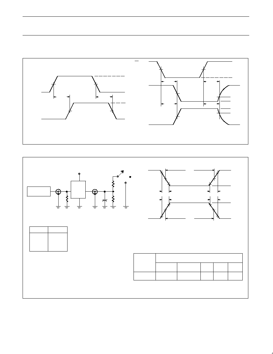
AC WAVEFORMS
V
M
= 1.5V, V
IN
= GND to 2.7V
nOE INPUT
tPZH
tPHZ
nYx
OUTPUT
V
OH
nYx
OUTPUT
V
OL
tPZL
tPLZ
3.0V
0V
V
OL
+ 0.3V
V
OH
0.3V
nAx
INPUT
nYx
OUTPUT
tPLH
tPHL
Waveform 1. Waveforms Showing the Input to Output
Propagation Delays
Waveform 2. Waveforms Showing the 3-State Output
Enable and Disable Times
1.5V
2.7V
0V
1.5V
1.5V
1.5V
2.7V
1.5V
1.5V
1.5V
1.5V
V
OH
V
OL
0V
TEST CIRCUIT AND WAVEFORMS
PULSE
GENERATOR
VIN
D.U.T
VOUT
CL
VCC
RL
Test Circuit for 3-State Outputs
VM
VM
tW
AMP (V)
NEGATIVE
PULSE
10%
10%
90%
90%
0V
VM
VM
tW
AMP (V)
POSITIVE
PULSE
90%
90%
10%
10%
0V
tTHL (tF)
tTLH (tR)
tTHL (tF)
tTLH (tR)
V
M
= 1.5V
Input Pulse Definition
DEFINITIONS
R
L
=
Load resistor; see AC CHARACTERISTICS for value.
C
L
=
Load capacitance includes jig and probe capacitance:
See AC CHARACTERISTICS for value.
R
T
= Termination resistance should be equal to Z
OUT
of
pulse generators.
INPUT PULSE REQUIREMENTS
FAMILY
Amplitude
Rep. Rate
t
W
t
R
t
F
74LVT16
2.7V
10MHz
500ns
2.5ns
2.5ns
SWITCH POSITION
TEST
SWITCH
t
PLZ/
t
PZL
6V
t
PLH/
t
PHL
Open
t
PHZ
/t
PZH
GND
6.0V
R
T
RL
Open
GND
Document Outline
- FEATURES
- DESCRIPTION
- QUICK REFERENCE DATA
- ORDERING INFORMATION
- LOGIC SYMBOL
- LOGIC SYMBOL (IEEE/IEC)
- PIN CONFIGURATION
- PIN DESCRIPTION
- FUNCTION TABLE
- ABSOLUTE MAXIMUM RATINGS
- RECOMMENDED OPERATING CONDITIONS
- DC ELECTRICAL CHARACTERISTICS
- AC CHARACTERISTICS
- AC WAVEFORMS
- TEST CIRCUIT AND WAVEFORMS