Äîêóìåíòàöèÿ è îïèñàíèÿ www.docs.chipfind.ru

Philips
Semiconductors
74LVT623
3.3 V octal transceiver with dual enable
(3-State)
Product specification
Supersedes data of 1996 Feb 15
IC24 Data Handbook
1999 Jul 09
INTEGRATED CIRCUITS
Philips Semiconductors
Product specification
74LVT623
3.3 V octal transceiver with dual enable (3-State)
2
1999 Jul 09
8532164 21957
FEATURES
·
Separate controls for data flow in each direction
·
Output capability: +64 mA/32 mA
·
TTL input and output switching levels
·
Input and output interface capability to systems at 5 V supply
·
Bus-hold data inputs eliminate the need for external pull-up
resistors to hold unused inputs
·
Live insertion/extraction permitted
·
No bus current loading when output is tied to 5 V bus
·
Power-up 3-State
·
Power-up reset
·
Latch-up protection exceeds 500 mA per JEDEC Std 17
·
ESD protection exceeds 2000 V per MIL STD 883 Method 3015
and 200 V per Machine Model
DESCRIPTION
The 74LVT623 is a high-performance BiCMOS product designed for
V
CC
operation at 3.3 V.
The 74LVT623 device is an octal transceiver featuring noninverting
3-State bus compatible outputs in both send and receive directions.
The 74LVT623 is designed for asynchronous two-way
communication between data buses. The control function
implementation allows for maximum flexibility in timing. This device
allows data transmission from the A bus to the B bus or from the B
bus to the A bus, depending upon the logic levels at the Enable
inputs (OEBA and OEAB). The Enable inputs can be used to disable
the device so that the buses are effectively isolated.
Control of data flow from B to A is similar, but using the EBA, LEBA,
and OEBA inputs.
QUICK REFERENCE DATA
SYMBOL
PARAMETER
CONDITIONS
T
amb
= 25
°
C; GND = 0V
TYPICAL
UNIT
t
PLH
t
PHL
Propagation delay
An to Bn or Bn to An
C
L
= 50pF;
V
CC
= 3.3 V
2.3
2.5
ns
C
IN
Input capacitance
V
I
= 0 V or 3.0 V
4
pF
C
I/O
I/O capacitance
Outputs disabled; V
I/O
= 0 V or 3.0 V
7
pF
I
CCZ
Total supply current
Outputs disabled; V
CC
= 3.6 V
0.13
mA
ORDERING INFORMATION
PACKAGES
TEMPERATURE RANGE
OUTSIDE NORTH AMERICA
NORTH AMERICA
DWG NUMBER
24-Pin Plastic SOL
40
°
C to +85
°
C
74LVT623 D
74LVT623 D
SOT137-1
24-Pin Plastic SSOP Type II
40
°
C to +85
°
C
74LVT623 DB
74LVT623 DB
SOT340-1
24-Pin Plastic TSSOP Type I
40
°
C to +85
°
C
74LVT623 PW
74LVT623PW DH
SOT355-1
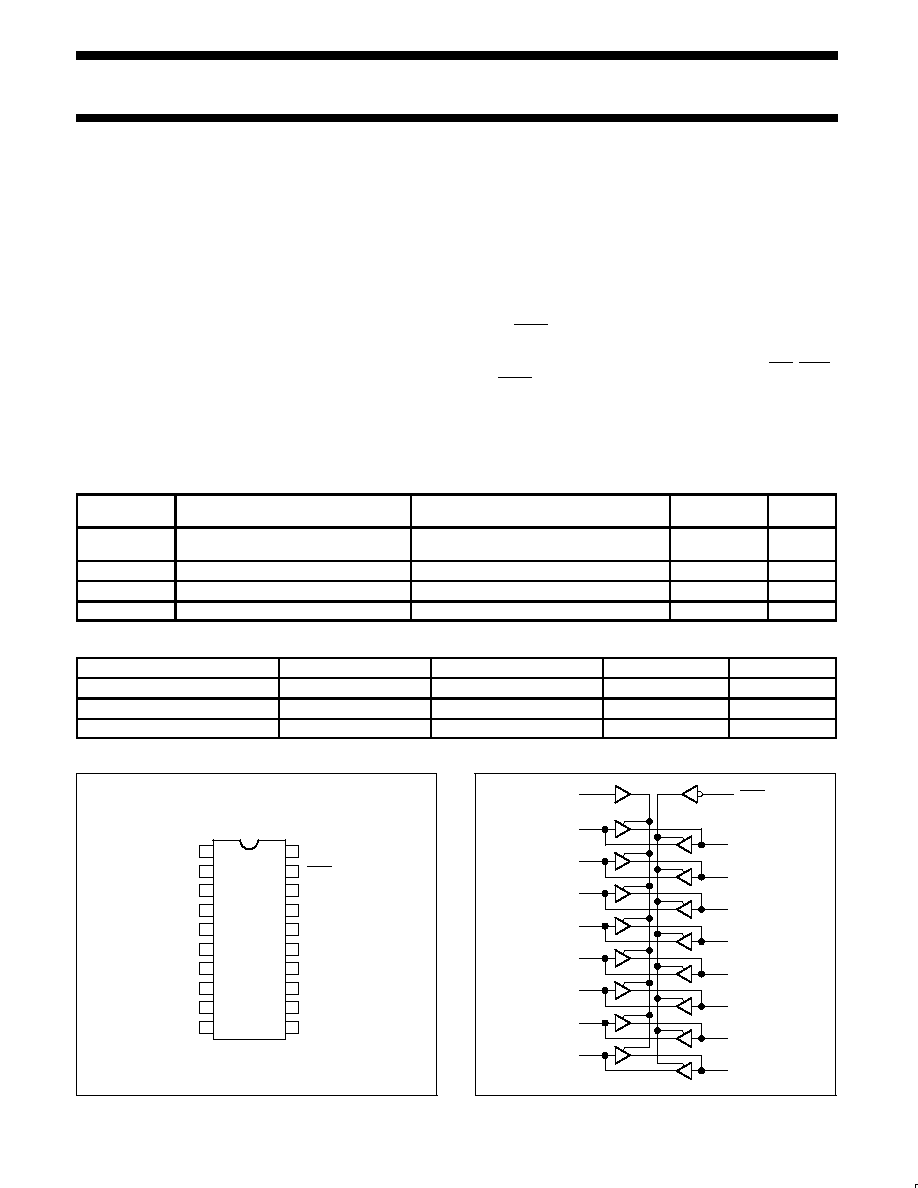
PIN CONFIGURATION
1
2
3
4
5
6
7
8
9
10
11
12
13
14
15
16
17
18
19
20
SA00189
OEAB
A0
A1
A2
A3
A4
A5
A6
A7
GND
V
CC
OEBA
B0
B1
B2
B3
B4
B5
B6
B7
LOGIC SYMBOL
OEBA
19
SA00195
OEAB
A0
A1
A2
A3
A4
A5
A6
A7
1
2
3
4
5
6
7
8
9
B0
B1
B1
B3
B4
B5
B6
B7
18
17
16
15
14
13
12
11
Philips Semiconductors
Product specification
74LVT623
3.3 V octal transceiver with dual enable (3-State)
1999 Jul 09
3
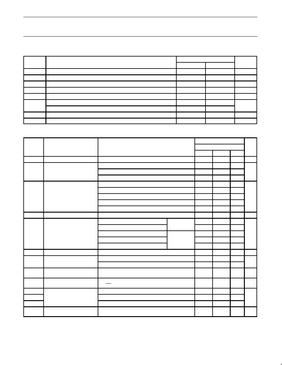
LOGIC SYMBOL (IEEE/IEC)
EN1
EN1
1
2
SA00196
1
19
2
3
4
5
6
7
8
9
18
17
16
15
14
13
12
11
PIN DESCRIPTION
PIN NUMBER
SYMBOL
NAME AND FUNCTION
1
OEAB
Output enable input, A side to B
side (active-High)
2, 3, 4, 5,
6, 7, 8, 9
A0 A7
Data inputs/outputs (A side)
18, 17, 16, 15,
14, 13, 12, 11
B0 B7
Data inputs/outputs (B side)
19
OEBA
Output enable input, B side to A
side (active-Low)
10
GND
Ground (0 V)
20
V
CC
Positive supply voltage
FUNCTION TABLE
INPUTS
INPUTS/OUTPUTS
OEBA
OEAB
An
Bn
L
L
An = Bn
Inputs
H
H
Inputs
Bn = An
H
L
Z
Z
L
H
An = Bn
Bn = An
H = High voltage level
L
= Low voltage level
Z = High impedance "off" state
ABSOLUTE MAXIMUM RATINGS
1, 2
SYMBOL
PARAMETER
CONDITIONS
RATING
UNIT
V
CC
DC supply voltage
0.5 to +4.6
V
I
IK
DC input diode current
V
I
< 0
50
mA
V
I
DC input voltage
3
0.5 to +7.0
V
I
OK
DC output diode current
V
O
< 0
50
mA
V
OUT
DC output voltage
3
Output in Off or High state
0.5 to +7.0
V
I
O
DC output current
Output in Low state
128
mA
I
OUT
DC output current
Output in High state
64
mA
T
stg
Storage temperature range
65 to 150
°
C
NOTES:
1. Stresses beyond those listed may cause permanent damage to the device. These are stress ratings only and functional operation of the
device at these or any other conditions beyond those indicated under "recommended operating conditions" is not implied. Exposure to
absolute-maximum-rated conditions for extended periods may affect device reliability.
2. The performance capability of a high-performance integrated circuit in conjunction with its thermal environment can create junction
temperatures which are detrimental to reliability. The maximum junction temperature of this integrated circuit should not exceed 150
°
C.
3. The input and output negative voltage ratings may be exceeded if the input and output clamp current ratings are observed.
Philips Semiconductors
Product specification
74LVT623
3.3 V octal transceiver with dual enable (3-State)
1999 Jul 09
4
RECOMMENDED OPERATING CONDITIONS
SYMBOL
PARAMETER
LIMITS
UNIT
SYMBOL
PARAMETER
MIN
MAX
UNIT
V
CC
DC supply voltage
2.7
3.6
V
V
I
Input voltage
0
5.5
V
V
IH
High-level input voltage
2.0
V
V
IL
Low-level input voltage
0.8
V
I
OH
High-level output current
32
mA
I
O
Low-level output current
32
mA
I
OL
Low-level output current; current duty cycle
50%; f
1 kHz
64
mA
t/
v
Input transition rise or fall rate; outputs enabled
10
ns/V
T
amb
Operating free-air temperature range
40
+85
°
C
DC ELECTRICAL CHARACTERISTICS
LIMITS
SYMBOL
PARAMETER
TEST CONDITIONS
Temp = -40
°
C to +85
°
C
UNIT
MIN
TYP
1
MAX
V
IK
Input clamp voltage
V
CC
= 2.7 V; I
IK
= 18 mA
0.9
1.2
V
V
CC
= 2.7 to 3.6 V; I
OH
= 100
µ
A
V
CC
-0.2
V
CC
-0.1
V
OH
High-level output voltage
V
CC
= 2.7 V; I
OH
= 8 mA
2.4
2.5
V
V
CC
= 3.0 V; I
OH
= 32 mA
2.0
2.2
V
CC
= 2.7 V; I
OL
= 100
µ
A
0.1
0.2
V
CC
= 2.7 V; I
OL
= 24 mA
0.3
0.5
V
OL
Low-level output voltage
V
CC
= 3.0 V; I
OL
= 16 mA
0.25
0.4
V
V
CC
= 3.0 V; I
OL
= 32 mA
0.3
0.5
V
CC
= 3.0 V; I
OL
= 64 mA
0.4
0.55
V
RST
Power-up output low voltage
5
V
CC
= 3.6 V; I
O
= 1 mA; V
I
= GND or V
CC
0.13
0.55
V
V
CC
= 3.6 V; V
I
= V
CC
or GND
Control pins
±
0.1
±
1
V
CC
= 0 or 3.6 V; V
I
= 5.5 V
Control pins
1
10
I
I
Input leakage current
V
CC
= 3.6 V; V
I
= 5.5 V
1
20
µ
A
V
CC
= 3.6 V; V
I
= V
CC
I/O Data pins
4
0.1
1
V
CC
= 3.6 V; V
I
= 0
1
-5
I
OFF
Output off current
V
CC
= 0 V; V
I
or V
O
= 0 to 4.5 V
1
±
100
µ
A
I
O
Bus Hold current
V
CC
= 3 V; V
I
= 0.8 V
75
150
µ
A
I
HOLD
A or B ports
V
CC
= 3 V; V
I
= 2.0 V
75
150
µ
A
I
EX
Current into an output in the
High state when V
O
> V
CC
V
O
= 5.5 V; V
CC
= 3.0 V
60
125
µ
A
I
PU/PD
Power up/down 3-State output
current
3
V
CC
1.2 V; V
O
= 0.5 V to V
CC
; V
I
= GND or V
CC
;
OE/OE = Don't care
15
±
100
µ
A
I
CCH
V
CC
= 3.6 V; Outputs High, V
I
= GND or V
CC,
I
O =
0
0.13
0.19
I
CCL
Quiescent supply current
V
CC
= 3.6 V; Outputs Low, V
I
= GND or V
CC,
I
O =
0
3
12
mA
I
CCZ
V
CC
= 3.6 V; Outputs Disabled; V
I
= GND or V
CC,
I
O =
0
0.13
0.19
I
CC
Additional supply current per
input pin
2
V
CC
= 3 V to 3.6 V; One input at V
CC
-0.6 V,
Other inputs at V
CC
or GND
0.1
0.2
mA
NOTES:
1. All typical values are at V
CC
= 3.3 V and T
amb
= 25
°
C.
2. This is the increase in supply current for each input at the specified voltage level other than V
CC
or GND
3. This parameter is valid for any V
CC
between 0V and 1.2V with a transition time of up to 10msec. From V
CC
= 1.2 V to V
CC
= 3.3 V
±
0.3 V a
transition time of 100
µ
sec is permitted. This parameter is valid for T
amb
= 25
°
C only.
4. Unused pins at V
CC
or GND.
5. For valid test results, data must not be loaded into the flip-flops (or latches) after applying the power.
Philips Semiconductors
Product specification
74LVT623
3.3 V octal transceiver with dual enable (3-State)
1999 Jul 09
5
AC CHARACTERISTICS
GND = 0 V, t
R
= t
F
= 2.5 ns, C
L
= 50 pF, R
L
= 500
; T
amb
= 40
°
C to +85
°
C.
LIMITS
SYMBOL
PARAMETER
WAVEFORM
V
CC
= 3.3 V
±
0.3 V
V
CC
= 2.7 V
UNIT
MIN
TYP
1
MAX
MAX
t
PLH
t
PHL
Propagation delay
An to Bn, Bn to An
1
1.0
1.0
2.3
2.5
3.5
3.7
4.3
4.1
ns
t
PZH
t
PZL
Output enable time
OEBA to An
2
3
1.0
1.1
3.7
3.7
5.9
5.9
7.6
6.8
ns
t
PHZ
t
PLZ
Output disable time
OEBA to An
2
3
1.8
1.8
3.6
3.2
5.0
4.5
5.5
4.6
ns
t
PZH
t
PZL
Output enable time
OEAB to Bn
2
3
1.0
1.4
4.2
4.3
6.3
6.2
7.8
6.9
ns
t
PHZ
t
PLZ
Output disable time
OEAB to Bn
2
3
2.3
2.0
3.9
3.6
6.1
5.3
6.9
5.8
ns
NOTE:
1. All typical values are at V
CC
= 3.3 V and T
amb
= 25
°
C.
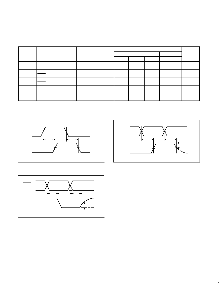
AC WAVEFORMS
V
M
= 1.5 V, V
IN
= GND to 2.7 V
tPLH
tPHL
V
IN
V
OUT
1.5V
1.5V
2.7V
0V
1.5V
1.5V
V
OH
V
OL
SV00113
Waveform 1.
Propagation Delay for Non-Inverting Output
OEBA,
OEAB
tPZH
tPHZ
0V
V
OH
0.3V
An, Bn
1.5V
1.5V
1.5V
0V
2.7V
V
OH
SV00169
Waveform 2.
3-State Output Enable Time to High Level
and Output Disable Time from High Level
tPZL
tPLZ
V
OL
+0.3V
OEBA,
OEAB
An, Bn
1.5V
1.5V
1.5V
2.7V
0V
3.0V
V
OL
SV00170
Waveform 3.
3-State Output Enable Time to Low Level
and Output Disable Time from Low Level