 | –≠–ª–µ–∫—Ç—Ä–æ–Ω–Ω—ã–π –∫–æ–º–ø–æ–Ω–µ–Ω—Ç: 74LVT74PW | –°–∫–∞—á–∞—Ç—å:  PDF PDF  ZIP ZIP |

Philips
Semiconductors
74LVT74
3.3V Dual D-type flip-flop
Product specification
1996 Aug 28
INTEGRATED CIRCUITS
IC24 Data Handbook
Philips Semiconductors
Product specification
74LVT74
3.3V Dual D-type flip-flop
2
1996 Aug 28
853-1872 17244
QUICK REFERENCE DATA
SYMBOL
PARAMETER
CONDITIONS
T
amb
= 25
∞
C;
GND = 0V
TYPICAL
UNIT
t
PLH
t
PHL
Propagation
delay
CPn to Qn
C
L
= 50pF;
V
CC
= 3.3V
3.1
3.6
ns
C
IN
Input
capacitance
V
I
= 0V or 3.0V
3
pF
I
CC
Total supply
current
V
CC
= 3.6V
0.5
mA
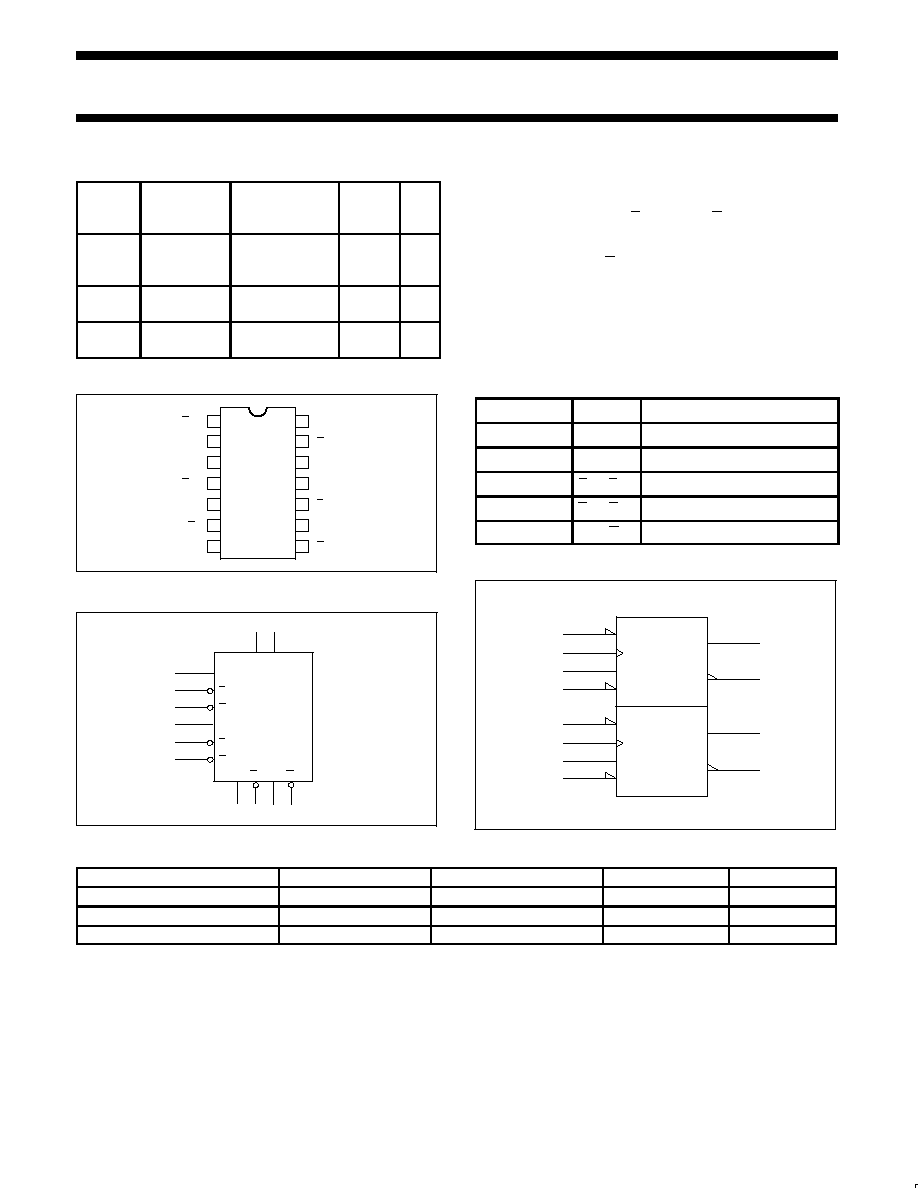
PIN CONFIGURATION
14
13
12
11
10
9
8
7
6
5
4
3
2
1
GND
V
CC
SD1
Q1
Q1
CP1
RD1
D1
RD0
D0
Q0
CP0
SD0
Q0
SF00045
LOGIC SYMBOL
Q0 Q0 Q1 Q1
5
6
9
8
V
CC
= Pin 14
GND = Pin 7
3
4
1
11
10
13
CP0
SD0
RD0
CP1
SD1
RD1
D0
D1
2
12
SA00359
DESCRIPTION
The 74LVT74 is a dual positive edge-triggered D-type flip-flop
featuring individual data, clock, set, and reset inputs; also true and
complementary outputs. Set (SD) and reset (RD) are asynchronous
active low inputs and operate independently of the clock input.
When set and reset are inactive (high), data at the D input is
transferred to the Q and Q outputs on the low-to-high transition of
the clock. Data must be stable just one setup time prior to the
low-to-high transition of the clock for predictable operation. Clock
triggering occurs at a voltage level and is not directly related to the
transition time of the positive-going pulse. Following the hold time
interval, data at the D input may be changed without affecting the
levels of the output.
PIN DESCRIPTION
PIN NUMBER
SYMBOL
NAME AND FUNCTION
2, 12
D0, D1
Data inputs
3, 11
CP0, CP1
Clock inputs (active rising edge)
4, 10
SD0, SD1
Set inputs (active LOW)
1, 13
RD0, RD1
Reset inputs (active LOW)
5, 6, 8, 9
Qn, Qn
Data outputs
LOGIC SYMBOL (IEEE/IEC)
4
3
2
1
10
11
12
13
5
6
9
8
&
S
S
C1
C2
R
1D
2D
R
SF00047
ORDERING INFORMATION
PACKAGES
TEMPERATURE RANGE
OUTSIDE NORTH AMERICA
NORTH AMERICA
DWG NUMBER
14-Pin Plastic SO
≠40
∞
C to +85
∞
C
74LVT74 D
74LVT74 D
SOT108-1
14-Pin Plastic SSOP
≠40
∞
C to +85
∞
C
74LVT74 DB
74LVT74 DB
SOT337-1
14-Pin Plastic TSSOP
≠40
∞
C to +85
∞
C
74LVT74 PW
74LVT74PW DH
SOT402-1

Philips Semiconductors
Product specification
74LVT74
3.3V Dual D-type flip-flop
1996 Aug 28
3
LOGIC DIAGRAM
V
CC
= Pin 14
GND = Pin 7
5, 9
6, 8
Q
Q
4, 10
1, 13
3, 11
2, 12
SD
RD
CP
D
SF00048
FUNCTION TABLE
INPUTS
OUTPUTS
OPERATING
SD
RD
CP
D
Q
Q
MODE
L
H
X
X
H
L
Asynchronous set
H
L
X
X
L
H
Asynchronous reset
L
L
X
X
H
H
Undetermined*
H
H
h
H
L
Load "1"
H
H
l
L
H
Load "0"
H
H
X
NC
NC
Hold
NOTES:
H = High voltage level
h
= High voltage level one setup time prior to low-to-high
clock transition
L
= Low voltage level
l
= Low voltage level one setup time prior to low-to-high
clock transition
NC= No change from the previous setup
X = Don't care
= Low-to-high clock transition
= Not low-to-high clock transition
*
= This setup is unstable and will change when either set
or reset return to the high level.
ABSOLUTE MAXIMUM RATINGS
1, 2
SYMBOL
PARAMETER
CONDITIONS
RATING
UNIT
V
CC
DC supply voltage
≠0.5 to +4.6
V
I
IK
DC input diode current
V
I
< 0
≠50
mA
V
I
DC input voltage
3
≠0.5 to +7.0
V
I
OK
DC output diode current
V
O
< 0
≠50
mA
V
OUT
DC output voltage
3
Output in Off or High state
≠0.5 to +7.0
V
I
OUT
DC output current
Output in High state
≠32
mA
I
OUT
DC out ut current
Output in Low state
64
mA
T
stg
Storage temperature range
≠65 to 150
∞
C
NOTES:
1. Stresses beyond those listed may cause permanent damage to the device. These are stress ratings only and functional operation of the
device at these or any other conditions beyond those indicated under "recommended operating conditions" is not implied. Exposure to
absolute-maximum-rated conditions for extended periods may affect device reliability.
2. The performance capability of a high-performance integrated circuit in conjunction with its thermal environment can create junction
temperatures which are detrimental to reliability. The maximum junction temperature of this integrated circuit should not exceed 150
∞
C.
3. The input and output negative voltage ratings may be exceeded if the input and output clamp current ratings are observed.
RECOMMENDED OPERATING CONDITIONS
SYMBOL
PARAMETER
LIMITS
UNIT
SYMBOL
PARAMETER
MIN
MAX
UNIT
V
CC
DC supply voltage
2.7
3.6
V
V
I
Input voltage
0
5.5
V
V
IH
High-level input voltage
2.0
V
V
IL
Low-level Input voltage
0.8
V
I
OH
High-level output current
≠20
mA
I
OL
Low-level output current
32
mA
t/
v
Input transition rise or fall rate; Outputs enabled
10
ns/V
T
amb
Operating free-air temperature range
≠40
+85
∞
C

Philips Semiconductors
Product specification
74LVT74
3.3V Dual D-type flip-flop
1996 Aug 28
4
DC ELECTRICAL CHARACTERISTICS
Over recommended operating conditions
Voltages are referenced to GND (ground = 0V)
LIMITS
SYMBOL
PARAMETER
TEST CONDITIONS
Temp = -40
∞
C to +85
∞
C
UNIT
MIN
TYP
1
MAX
V
IK
Input clamp voltage
V
CC
= 2.7V; I
IK
= ≠18mA
≠1.2
V
V
CC
= 2.7 to 3.6V; I
OH
= ≠100
µ
A
V
CC
≠0.2
V
OH
High-level output voltage
V
CC
= 2.7V; I
OH
= ≠6mA
2.4
V
V
CC
= 3.0V; I
OH
= ≠20mA
2.0
V
CC
= 2.7V; I
OL
= 100
µ
A
0.2
V
OL
Low-level output voltage
V
CC
= 2.7V; I
OL
= 24mA
0.5
V
V
CC
= 3.0V; I
OL
= 32mA
0.5
I
I
Input leakage current
V
CC
= 0 or 3.6V; V
I
= 5.5V
10
µ
A
I
I
In ut leakage current
V
CC
= 3.6V; V
I
= V
CC
or GND
±
1
µ
A
I
OFF
Output off current
V
CC
= 0V; V
I
or V
O
= 0 to 4.5V
±
100
µ
A
I
CC
Quiescent supply current
V
CC
= 3.6V; Outputs High, V
I
= GND or
V
CC,
I
O =
0
0.5
1
mA
I
CC
Additional supply current per input pin
2
V
CC
= 3V to 3.6V; One input at V
CC
≠0.6V,
Other inputs at V
CC
or GND
0.2
µ
A
C
I
Input capacitance
V
I
= 3V or 0
3
pF
NOTES:
1. All typical values are at V
CC
= 3.3V and T
amb
= 25
∞
C.
2. This is the increase in supply current for each input at the specificed voltage level other than V
CC
or GND.
AC CHARACTERISTICS
GND = 0V; t
R
= t
F
= 2.5ns; C
L
= 50pF, R
L
= 500
; T
amb
= ≠40
∞
C to +85
∞
C.
LIMITS
SYMBOL
PARAMETER
WAVEFORM
V
CC
= 3.3V
±
0.3V
V
CC
= 2.7V
UNIT
MIN
TYP
1
MAX
MAX
f
MAX
Maximum clock frequency
1
150
345
MHz
t
PLH
t
PHL
Propagation delay
CPn to Qn or Qn
1
1.0
1.0
3.1
3.6
4.8
5.0
5.8
5.0
ns
t
PLH
t
PHL
Propagation delay
SDn, RDn to Qn or Qn
2
1.0
1.0
3.1
3.0
5.0
4.4
6.2
4.8
ns
NOTE:
1. All typical values are at V
CC
= 3.3V and T
amb
= 25
∞
C.
AC SETUP REQUIREMENTS
LIMITS
SYMBOL
PARAMETER
WAVEFORM
V
CC
= 3.3V
±
0.3V
V
CC
= 2.7V
UNIT
MIN
TYP
MIN
t
S
(H)
t
S
(L)
Setup time
Dn to CPn
1
1.7
1.4
0.6
0.4
1.8
1.6
ns
t
h
(H)
t
h
(L)
Holdtime
Dn to CPn
1
0.3
0
≠0.3
≠0.6
0.3
0
ns
t
W
(H)
t
W
(L)
CPn Pulse Width
1
2.0
2.0
1.0
1.2
3.0
3.0
ns
t
W
(L)
SDn, RDn Pulse Width
2
2.0
1.0
3.0
t
rec
Recovery time
SDn, RDn tp CPn
3
0.5
≠0.3
0.5
ns

Philips Semiconductors
Product specification
74LVT74
3.3V Dual D-type flip-flop
1996 Aug 28
5
AC WAVEFORMS
V
M
= 1.5V, V
IN
= GND to 2.7V
VM
VM
CPn
VM
VM
VM
VM
VM
VM
tsu(H)
th(H)
Dn
Qn
VM
tw(H)
1/fmax
tsu(L)
th(L)
VM
VM
tPLH
Qn
tw(L)
tPHL
tPHL
tPLH
SF00049
Waveform 1.
Propagation delay for data to output,
data setup time and hold times, and clock width,
and maximum clock frequency
VM
VM
RDn
VM
Qn
VM
VM
VM
tPLH
Qn
tw(L)
tPHL
tPHL
tPLH
SDn
VM
VM
tw(L)
SF00050
Waveform 2.
Propagation delay for set and reset to output,
set and reset pulse width
SDn or RDn
VM
VM
trec
CPn
SF00051
Waveform 3.
Recovery time for set or reset to clock
TEST CIRCUIT AND WAVEFORMS
VM
VM
tW
AMP (V)
NEGATIVE
PULSE
10%
10%
90%
90%
0V
VM
VM
tW
AMP (V)
POSITIVE
PULSE
90%
90%
10%
10%
0V
tTHL (tF)
tTLH (tR)
tTHL (tF)
tTLH (tR)
V
M
= 1.5V
Input Pulse Definition
DEFINITIONS
R
L
=
Load resistor; see AC CHARACTERISTICS for value.
C
L
=
Load capacitance includes jig and probe capacitance;
see AC CHARACTERISTICS for value.
R
T
=
Termination resistance should be equal to Z
OUT
of
pulse generators.
INPUT PULSE REQUIREMENTS
FAMILY
Amplitude
Rep. Rate
t
W
t
R
t
F
74LVT
2.7V
10MHz
500ns
2.5ns
2.5ns
PULSE
GENERATOR
VIN
D.U.T.
VOUT
CL
VCC
Test Circuit for Outputs
R
T
RL
SV00022