Philips Semiconductors
Product specification
80CL410/83CL410
Low voltage/low power single-chip
8-bit microcontroller with I
2
C
2
1995 Jan 20
DESCRIPTION
The 80CL410/83CL410 (hereafter generically
referred to as 8XCL410) is manufactured in
an advanced CMOS process that allows the
part to operate at supply voltages down to
1.8V and oscillator frequencies down to DC.
The 8XCL410 has the same instruction set
as the 80C51.
The 8XCL410 features a 4k byte ROM
(83CL410), 128 bytes RAM (both ROM and
RAM are externally expandable to 64k
bytes), four 8-bit ports, two 16-bit
timer/counters, an I
2
C serial interface, a
thirteen source, two priority level nested
interrupt structure, and on-chip oscillator
circuitry suitable for quartz crystal, ceramic
resonator, RC, or LC.
The 8XCL410 has two reduced power modes
that are the same as those on the standard
80C51. The special reduced power feature of
this part is that it can be stopped and then
restarted. Running from an external clock
source, the clock can be stopped and after a
period of time restarted. The 8XCL410 will
resume operation from where it was when the
code stopped with no loss of internal state,
RAM contents, or Special Function Register
contents. If the internal oscillator is used the
part cannot be stopped and started, but the
power-down mode, which can be terminated
via an interrupt, can be used to achieve
similar power savings and then restart
without loss of on-chip RAM and Special
Function Register values.
FEATURES
�
Single supply voltage 1.8V to 6.0V
�
Frequency from DC to 12MHz
�
80C51 based architecture
� 4k
�
8 ROM (64k external)
� 128
�
8 RAM (64k external)
� Four 8-bit I/O ports
� Two 16-bit timer/counters
� A thirteen-source, two-level, nested
priority interrupt structure
� 10 external interrupts
�
Fully static 80C51 CPU
�
I
2
C Serial Interface
�
Two power control modes
� Idle mode
� Power-down mode � can be terminated
by reset or external interrupt
�
Wake-up via external interrupts at port 1
�
Single supply voltage 1.8V to 6.0V
�
Frequency range of DC to 12MHz
�
On-chip oscillator (quartz crystal, ceramic
resonator, RC, LC)
�
Very low power consumption
�
Operating temperature range:
�40 to +85
�
C
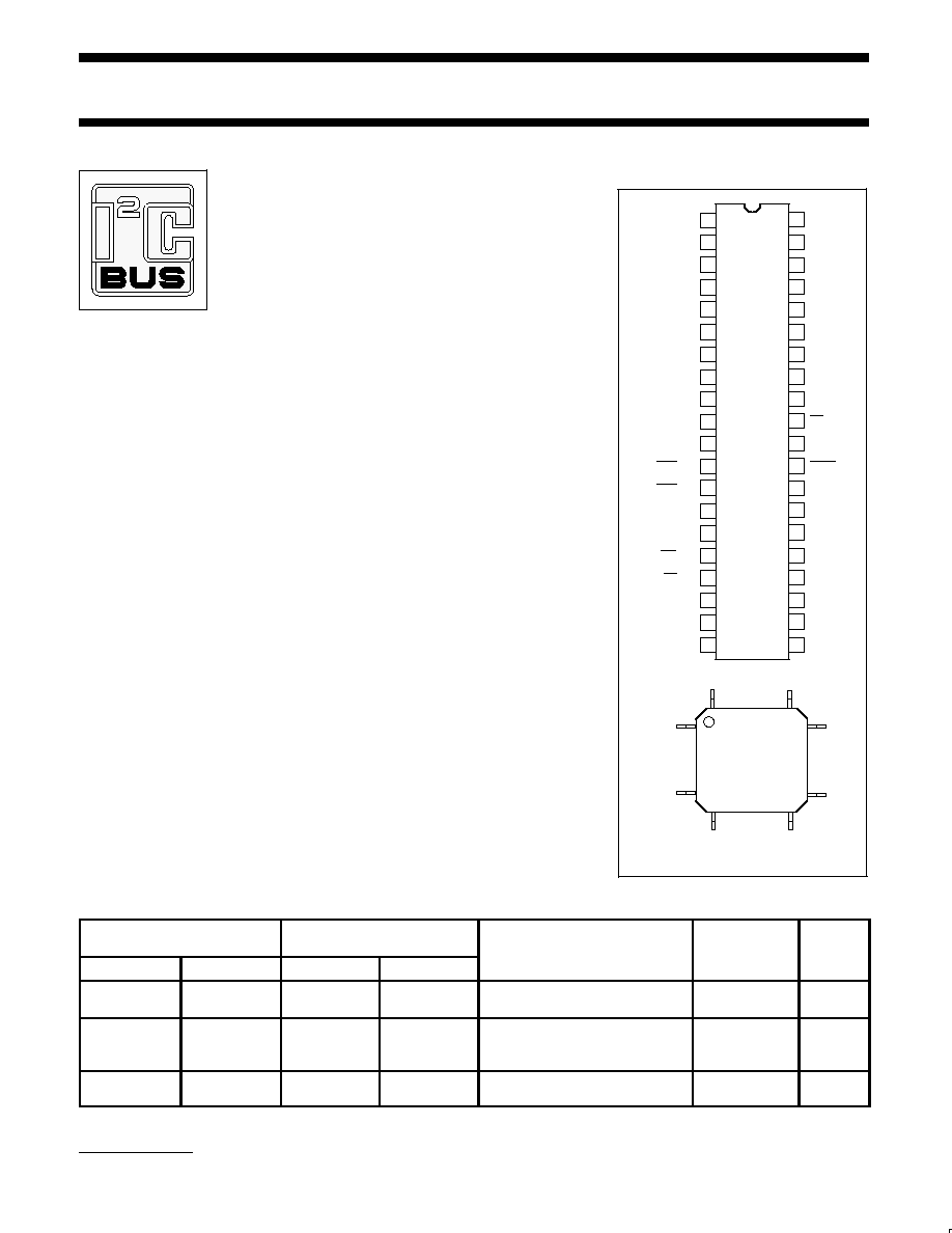
PIN CONFIGURATION
P2.0/A8
P2.1/A9
P2.2/A10
P2.3/A11
P2.4/A12
P2.5/A13
P2.6/A14
P2.7/A15
PSEN
ALE
EA
P0.7/AD7
P0.6/AD6
P0.5/AD5
P0.4/AD4
P0.3/AD3
P0.2/AD2
P0.1/AD1
P0.0/AD0
VDD
DIP
VSO
20
21
VSS
SCL/INT8/P1.6
1
2
3
4
5
6
7
8
9
10
11
12
13
14
15
16
17
18
19
22
23
24
25
26
27
28
29
30
31
32
33
34
35
36
37
38
39
40
INT2/P1.0
INT3/P1.1
INT4/P1.2
INT5/P1.3
INT6/P1.4
INT7/P1.5
RST
P3.0
P3.1
INT0/P3.2
INT1/P3.3
T0/P3.4
T1/P3.5
SDA/INT9/P1.7
WR/P3.6
RD/P3.7
XTAL2
XTAL1
44
34
1
11
33
23
12
22
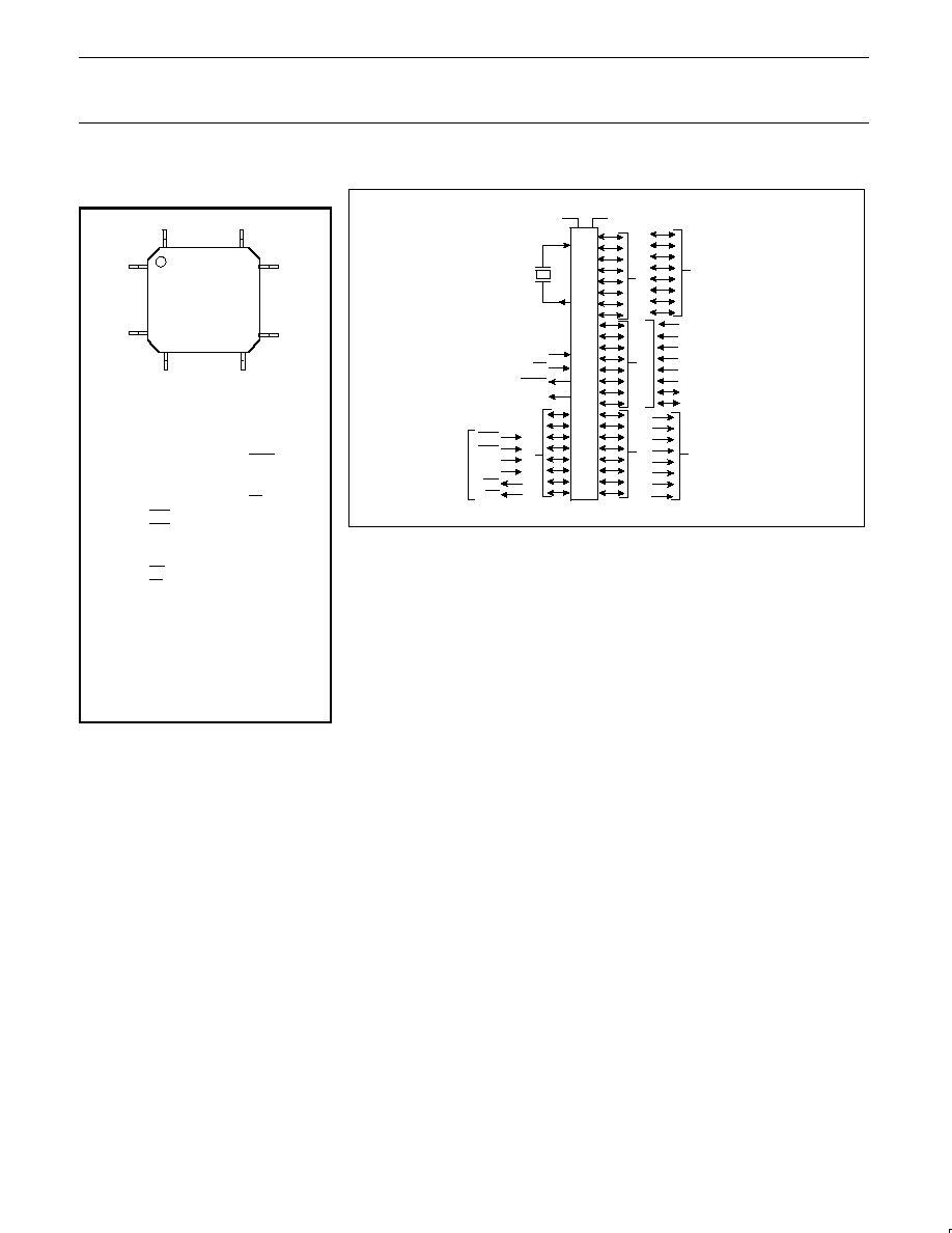
QFP
SEE NEXT PAGE FOR QFP PIN FUNCTIONS.
ORDERING CODE
PHILIPS PART ORDER NUMBER
PART MARKING
PHILIPS NORTH AMERICA
PART ORDER NUMBER
1
TEMPERATURE
�
C
AND PACKAGE
Drawing
Number
ROMless
ROM
ROMless
ROM
AND PACKAGE
FREQUENCY
Number
P80CL410HFP
P83CL410HFP
P80CL410HF N
P83CL410HF N
�40 to +85,
40-Pin Plastic Dual In-line Package
32kHZ to 12MHz
SOT129-1
P80CL410HFT
P83CL410HFT
P80CL410HF D
P83CL410HF D
�40 to +85,
40-Pin Plastic Very Small Outline
Package
32kHZ to 12MHz
SOT158-1
P83CL410HFH
�40 to +85,
44-Pin Plastic Quad Flat Pack
32kHZ to 12MHz
SOT307-2
NOTE:
1. Parts ordered by the Philips North America part number will be marked with the Philips part marking.
For emulation purposes, the P85CL000 (Piggyback version) with 256 bytes of RAM is recommended.
Philips Semiconductors
Product specification
80CL410/83CL410
Low voltage/low power single-chip
8-bit microcontroller with I
2
C
1995 Jan 20
5
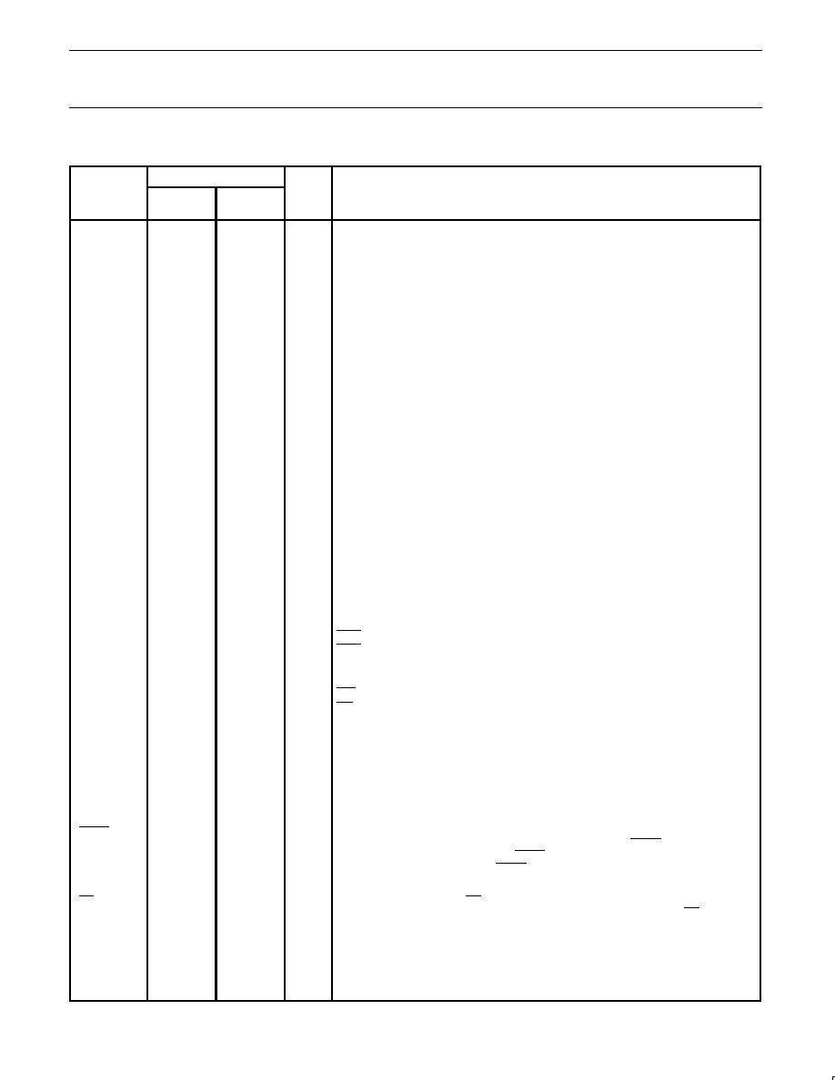
PIN DESCRIPTION
MNEMONIC
PIN NO.
TYPE
NAME AND FUNCTION
MNEMONIC
QFP
DIL40/
VSO40
TYPE
NAME AND FUNCTION
V
SS
16
20
I
Ground: 0V reference.
V
DD
38
40
I
Power Supply: This is the power supply voltage for normal, idle, and power-down
operation.
P0.0�0.7
30�37
39�32
I/O
Port 0: Port 0 is an open-drain, bidirectional I/O port. Port 0 pins that have 1s written
to them float and can be used as high-impedance inputs. Port 0 is also the multiplexed
low-order address and data bus during accesses to external program and data
memory. In this application, it uses strong internal pull-ups when emitting 1s.
P1.0�P1.7
40�44
1�3
1�8
I/O
Port 1: Port 1 is an 8-bit bidirectional I/O port with internal pull-ups. Port 1 pins that
have 1s written to them are pulled high by the internal pull-ups and can be used as
inputs. As inputs, port 1 pins that are externally pulled low will source current because
of the internal pull-ups. (See DC Electrical Characteristics: I
IL
). Additional functions
include:
7
I/O
SCL (P1.6): I
2
C serial bus clock.
8
I/O
SDA (P1.7): I
2
C serial bus data.
1�8
I
INT2�INT9 (P1.0�P1.7): Additional external interrupts.
P2.0�P2.7
18�25
21�28
I/O
Port 2: Port 2 is an 8-bit bidirectional I/O port with internal pull-ups. Port 2 pins that
have 1s written to them are pulled high by the internal pull-ups and can be used as
inputs. As inputs, port 2 pins that are externally being pulled low will source current
because of the internal pull-ups. (See DC Electrical Characteristics: I
IL
). Port 2 emits
the high-order address byte during fetches from external program memory and during
accesses to external data memory that use 16-bit addresses (MOVX @DPTR). In this
application, it uses strong internal pull-ups when emitting 1s. During accesses to
external data memory that use 8-bit addresses (MOV @Ri), port 2 emits the contents
of the P2 special function register.
P3.0�P3.7
5, 7�13
10�17
I/O
Port 3: Port 3 is an 8-bit bidirectional I/O port with internal pull-ups. Port 3 pins that
have 1s written to them are pulled high by the internal pull-ups and can be used as
inputs. As inputs, port 3 pins that are externally being pulled low will source current
because of the pull-ups. (See DC Electrical Characteristics: I
IL
). Port 3 also serves the
special features of the 80C51 family, as listed below:
8
12
I
INT0 (P3.2): External interrupt 0
9
13
I
INT1 (P3.3): External interrupt 1
10
14
I
T0 (P3.4): Timer 0 external input
11
15
I
T1 (P3.5): Timer 1 external input
12
16
O
WR (P3.6): External data memory write strobe
13
17
O
RD (P3.7): External data memory read strobe
RST
4
9
I
Reset: A high on this pin for two machine cycles while the oscillator is running, resets
the device. An internal diffused resistor to V
SS
permits a power-on reset using only an
external capacitor to V
DD
.
ALE
27
30
O
Address Latch Enable: Output pulse for latching the low byte of the address during
an access to external memory. In normal operation, ALE is emitted at a constant rate
of 1/6 the oscillator frequency, and can be used for external timing or clocking. Note
that one ALE pulse is skipped during each access to external data memory.
PSEN
26
29
O
Program Store Enable: The read strobe to external program memory. When the
device is executing code from the external program memory, PSEN is activated twice
each machine cycle, except that two PSEN activations are skipped during each
access to external data memory. PSEN is not activated during fetches from internal
program memory.
EA
29
31
I
External Access Enable: EA must be externally held low to enable the device to
fetch code from external program memory locations 0000H to 0FFFH. If EA is held
high, the device executes from internal program memory unless the program counter
contains an address greater than 0FFFH.
XTAL1
15
19
I
Crystal 1: Input to the inverting oscillator amplifier and input for an external clock
source.
XTAL2
14
18
O
Crystal 2: Output from the inverting oscillator amplifier.