 | –≠–ª–µ–∫—Ç—Ä–æ–Ω–Ω—ã–π –∫–æ–º–ø–æ–Ω–µ–Ω—Ç: 83C54 | –°–∫–∞—á–∞—Ç—å:  PDF PDF  ZIP ZIP |

Philips
Semiconductors
8XC52/54/58/80C32
8XC51FA/FB/FC/80C51FA
8XC51RA+/RB+/RC+/RD+/80C51RA +
80C51 8-bit microcontroller family
8K≠64K/256≠1K OTP/ROM/ROMless,
low voltage (2.7V≠5.5V), low power, high speed (33 MHz)
Product specification
Supersedes data of 1998 Jun 04
IC20 Data Handbook
1999 Apr 01
INTEGRATED CIRCUITS

Philips Semiconductors
Product specification
8XC52/54/58/80C32
8XC51FA/FB/FC/80C51FA
8XC51RA+/RB+/RC+/RD+/80C51RA+
80C51 8-bit microcontroller family
8K≠64K/256≠1K OTP/ROM/ROMless, low voltage (2.7V≠5.5V),
low power, high speed (33 MHz)
2
1999 Apr 01
853-2068 21142
DESCRIPTION
Three different Single-Chip 8-Bit Microcontroller families are
presented in this datasheet:
∑
80C32/8XC52/8XC54/8XC58
∑
80C51FA/8XC51FA/8XC51FB/8XC51FC
∑
80C51RA+/8XC51RA+/8XC51RB+/8XC51RC+/8XC51RD+
For applications requiring 4K ROM/EPROM, see the 8XC51/80C31
8-bit CMOS (low voltage, low power, and high speed)
microcontroller families datasheet.
All the families are Single-Chip 8-Bit Microcontrollers manufactured
in advanced CMOS process and are derivatives of the 80C51
microcontroller family. All the devices have the same instruction set
as the 80C51.
These devices provide architectural enhancements that make them
applicable in a variety of applications for general control systems.
ROM/EPROM
Memory Size
(X by 8)
RAM Size
(X by 8)
Programmable
Timer Counter
(PCA)
Hardware
Watch Dog
Timer
80C31/8XC51
0K/4K
128
No
No
80C32/8XC52/54/58
0K/8K/16K/32K
256
No
No
80C51FA/8XC51FA/FB/FC
0K/8K/16K/32K
256
Yes
No
80C51RA+/8XC51RA+/RB+/RC+
0K/8K/16K/32K
512
Yes
Yes
8XC51RD+
64K
1024
Yes
Yes
The ROMless devices, 80C32, 80C51FA, and 80C51RA+ can
address up to 64K of external memory. All the devices have four
8-bit I/O ports, three 16-bit timer/event counters, a multi-source,
four-priority-level, nested interrupt structure, an enhanced UART
and on-chip oscillator and timing circuits. For systems that require
extra memory capability up to 64k bytes, each can be expanded
using standard TTL-compatible memories and logic.
Its added features make it an even more powerful microcontroller for
applications that require pulse width modulation, high-speed I/O and
up/down counting capabilities such as motor control. It also has a
more versatile serial channel that facilitates multiprocessor
communications.
FEATURES
∑
80C51 Central Processing Unit
∑
Speed up to 33MHz
∑
Full static operation
∑
Operating voltage range:
2.7V to 5.5V @ 16MHz
∑
Security bits:
≠ ROM ≠ 2 bits
≠ OTP≠EPROM ≠ 3 bits
∑
Encryption array ≠ 64 bytes
∑
RAM expandable to 64K bytes
∑
4 level priority interrupt
∑
6 or7 interrupt sources, depending on device
∑
Four 8-bit I/O ports
∑
Full-duplex enhanced UART
≠ Framing error detection
≠ Automatic address recognition
∑
Power control modes
≠ Clock can be stopped and resumed
≠ Idle mode
≠ Power down mode
∑
Programmable clock out
∑
Second DPTR register
∑
Asynchronous port reset
∑
Low EMI (inhibit ALE)
Philips Semiconductors
Product specification
8XC52/54/58/80C32
8XC51FA/FB/FC/80C51FA
8XC51RA+/RB+/RC+/RD+/80C51RA+
80C51 8-bit microcontroller family
8K≠64K/256≠1K OTP/ROM/ROMless, low voltage (2.7V≠5.5V),
low power, high speed (33 MHz)
1999 Apr 01
3
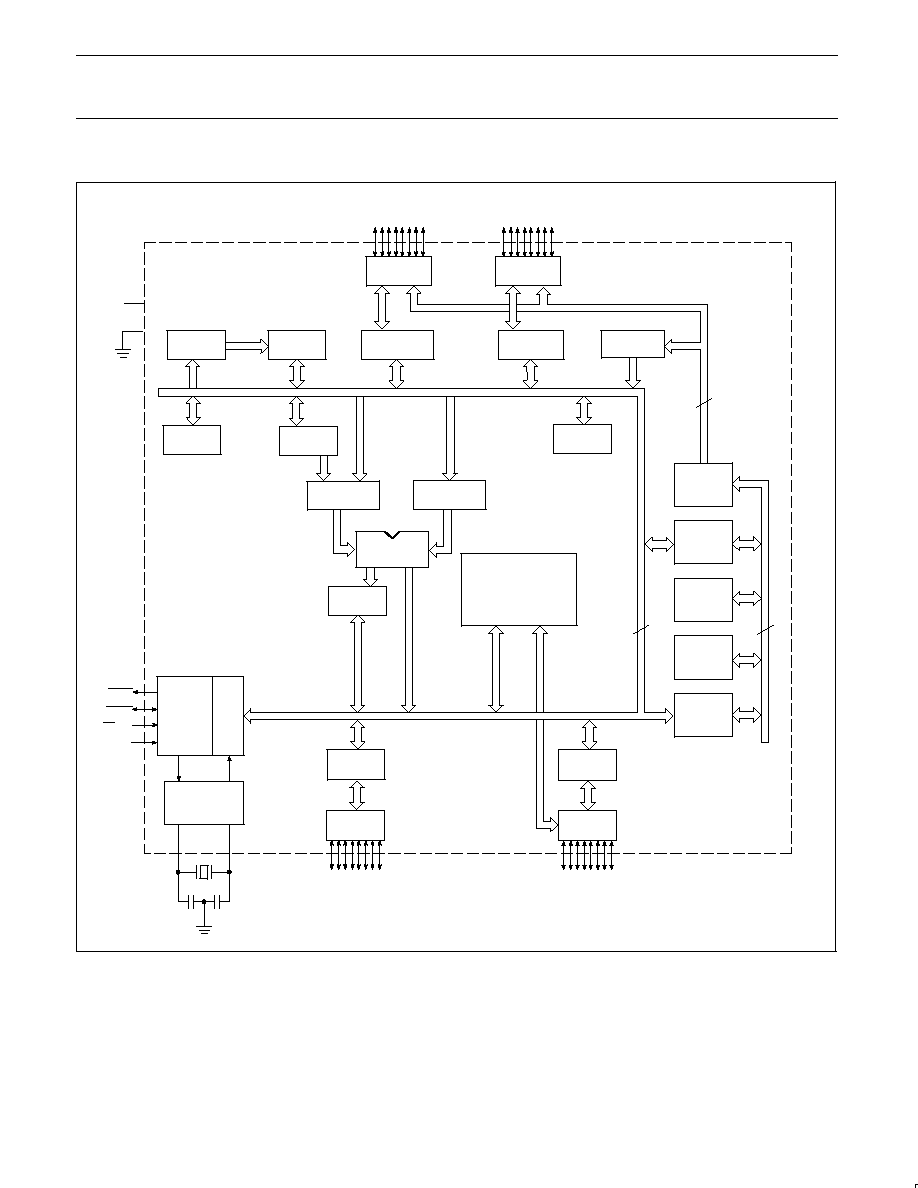
BLOCK DIAGRAM
PSEN
EAV
PP
ALE/PROG
RST
XTAL1
XTAL2
VCC
VSS
PORT 0
DRIVERS
PORT 2
DRIVERS
RAM ADDR
REGISTER
RAM
PORT 0
LATCH
PORT 2
LATCH
ROM/EPROM
REGISTER
B
ACC
STACK
POINTER
TMP2
TMP1
ALU
TIMING
AND
CONTROL
INSTRUCTION
REGISTER
PD
OSCILLATOR
PSW
PORT 1
LATCH
PORT 3
LATCH
PORT 1
DRIVERS
PORT 3
DRIVERS
PROGRAM
ADDRESS
REGISTER
BUFFER
PC
INCRE-
MENTER
PROGRAM
COUNTER
DPTR'S
MULTIPLE
P1.0≠P1.7
P3.0≠P3.7
P0.0≠P0.7
P2.0≠P2.7
SFRs
TIMERS
P.C.A. (FA & RA+ only)
SU00831B
8
8
16

Philips Semiconductors
Product specification
8XC52/54/58/80C32
8XC51FA/FB/FC/80C51FA
8XC51RA+/RB+/RC+/RD+/80C51RA+
80C51 8-bit microcontroller family
8K≠64K/256≠1K OTP/ROM/ROMless, low voltage (2.7V≠5.5V),
low power, high speed (33 MHz)
1999 Apr 01
4
LOGIC SYMBOL
POR
T
0
POR
T
1
POR
T
2
POR
T
3
ADDRESS AND
DATA BUS
ADDRESS BUS
T2
T2EX
RxD
TxD
INT0
INT1
T0
T1
WR
RD
SECONDAR
Y
FUNCTIONS
RST
EA/V
PP
PSEN
ALE/PROG
V
SS
V
CC
XTAL1
XTAL2
SU00830
PIN CONFIGURATIONS
DUAL IN-LINE PACKAGE PIN FUNCTIONS
1
2
3
4
5
6
7
8
9
10
11
12
13
14
15
16
17
18
19
20
21
22
23
24
25
26
27
28
29
30
31
32
33
34
35
36
37
38
39
40
T2/P1.0
T2EX/P1.1
ECI/P1.2
CEX0/P1.3
CEX1/P1.4
CEX2/P1.5
CEX3/P1.6
RST
RxD/P3.0
TxD/P3.1
INT0/P3.2
INT1/P3.3
T0/P3.4
T1/P3.5
CEX4/P1.7
WR/P3.6
RD/P3.7
XTAL2
XTAL1
V
SS
P2.0/A8
P2.1/A9
P2.2/A10
P2.3/A11
P2.4/A12
P2.5/A13
P2.6/A14
P2.7/A15
PSEN
ALE/PROG
EA/V
PP
P0.7/AD7
P0.6/AD6
P0.5/AD5
P0.4/AD4
P0.3/AD3
P0.2/AD2
P0.1/AD1
P0.0/AD0
V
CC
DUAL
IN-LINE
PACKAGE
SU00021
PLASTIC LEADED CHIP CARRIER PIN FUNCTIONS
LCC
6
1
40
7
17
39
29
18
28
Pin
Function
1
NIC*
2
P1.0/T2
3
P1.1/T2EX
4
P1.2/ECI
5
P1.3/CEX0
6
P1.4/CEX1
7
P1.5/CEX2
8
P1.6/CEX3
9
P1.7/CEX4
10
RST
11
P3.0/RxD
12
NIC*
13
P3.1/TxD
14
P3.2/INT0
15
P3.3/INT1
Pin
Function
16
P3.4/T0
17
P3.5/T1
18
P3.6/WR
19
P3.7/RD
20
XTAL2
21
XTAL1
22
V
SS
23
NIC*
24
P2.0/A8
25
P2.1/A9
26
P2.2/A10
27
P2.3/A11
28
P2.4/A12
29
P2.5/A13
30
P2.6/A14
Pin
Function
31
P2.7/A15
32
PSEN
33
ALE/PROG
34
NIC*
35
EA/V
PP
36
P0.7/AD7
37
P0.6/AD6
38
P0.5/AD5
39
P0.4/AD4
40
P0.3/AD3
41
P0.2/AD2
42
P0.1/AD1
43
P0.0/AD0
44
V
CC
SU00023
* NO INTERNAL CONNECTION
PLASTIC QUAD FLAT PACK
PIN FUNCTIONS
PQFP
44
34
1
11
33
23
12
22
Pin
Function
1
P1.5/CEX2
2
P1.6/CEX3
3
P1.7/CEX4
4
RST
5
P3.0/RxD
6
NIC*
7
P3.1/TxD
8
P3.2/INT0
9
P3.3/INT1
10
P3.4/T0
11
P3.5/T1
12
P3.6/WR
13
P3.7/RD
14
XTAL2
15
XTAL1
Pin
Function
16
V
SS
17
NIC*
18
P2.0/A8
19
P2.1/A9
20
P2.2/A10
21
P2.3/A11
22
P2.4/A12
23
P2.5/A13
24
P2.6/A14
25
P2.7/A15
26
PSEN
27
ALE/PROG
28
NIC*
29
EA/V
PP
30
P0.7/AD7
Pin
Function
31
P0.6/AD6
32
P0.5/AD5
33
P0.4/AD4
34
P0.3/AD3
35
P0.2/AD2
36
P0.1/AD1
37
P0.0/AD0
38
V
CC
39
NIC*
40
P1.0/T2
41
P1.1/T2EX
42
P1.2/ECI
43
P1.3/CEX0
44
P1.4/CEX1
SU00024
* NO INTERNAL CONNECTION
Philips Semiconductors
Product specification
8XC52/54/58/80C32
8XC51FA/FB/FC/80C51FA
8XC51RA+/RB+/RC+/RD+/80C51RA+
80C51 8-bit microcontroller family
8K≠64K/256≠1K OTP/ROM/ROMless, low voltage (2.7V≠5.5V),
low power, high speed (33 MHz)
1999 Apr 01
5
PIN DESCRIPTIONS
PIN NUMBER
MNEMONIC
DIP
LCC
QFP
TYPE
NAME AND FUNCTION
V
SS
20
22
16
I
Ground: 0V reference.
V
CC
40
44
38
I
Power Supply: This is the power supply voltage for normal, idle, and power-down operation.
P0.0≠0.7
39≠32
43≠36
37≠30
I/O
Port 0: Port 0 is an open-drain, bidirectional I/O port. Port 0 pins that have 1s written to
them float and can be used as high-impedance inputs. Port 0 is also the multiplexed
low-order address and data bus during accesses to external program and data memory. In
this application, it uses strong internal pull-ups when emitting 1s. Port 0 also outputs the
code bytes during program verification and received code bytes during EPROM
programming. External pull-ups are required during program verification.
P1.0≠P1.7
1≠8
2≠9
40≠44,
1≠3
I/O
Port 1: Port 1 is an 8-bit bidirectional I/O port with internal pull-ups. Port 1 pins that have 1s
written to them are pulled high by the internal pull-ups and can be used as inputs. As inputs,
port 1 pins that are externally pulled low will source current because of the internal pull-ups.
(See DC Electrical Characteristics: I
IL
). Port 1 also receives the low-order address byte
during program memory verification.
Alternate functions for 8XC51FX and 8XC51RX+ Port 1 include:
1
2
40
I/O
T2 (P1.0): Timer/Counter 2 external count input/Clockout (see Programmable Clock-Out)
2
3
41
I
T2EX (P1.1): Timer/Counter 2 Reload/Capture/Direction Control
3
4
42
I
ECI (P1.2): External Clock Input to the PCA
4
5
43
I/O
CEX0 (P1.3): Capture/Compare External I/O for PCA module 0
5
6
44
I/O
CEX1 (P1.4): Capture/Compare External I/O for PCA module 1
6
7
1
I/O
CEX2 (P1.5): Capture/Compare External I/O for PCA module 2
7
8
2
I/O
CEX3 (P1.6): Capture/Compare External I/O for PCA module 3
8
9
3
I/O
CEX4 (P1.7): Capture/Compare External I/O for PCA module 4
P2.0≠P2.7
21≠28
24≠31
18≠25
I/O
Port 2: Port 2 is an 8-bit bidirectional I/O port with internal pull-ups. Port 2 pins that have 1s
written to them are pulled high by the internal pull-ups and can be used as inputs. As inputs,
port 2 pins that are externally being pulled low will source current because of the internal
pull-ups. (See DC Electrical Characteristics: I
IL
). Port 2 emits the high-order address byte
during fetches from external program memory and during accesses to external data memory
that use 16-bit addresses (MOVX @DPTR). In this application, it uses strong internal
pull-ups when emitting 1s. During accesses to external data memory that use 8-bit addresses
(MOV @Ri), port 2 emits the contents of the P2 special function register. Some Port 2 pins
receive the high order address bits during EPROM programming and verification.
P3.0≠P3.7
10≠17
11,
13≠19
5,
7≠13
I/O
Port 3: Port 3 is an 8-bit bidirectional I/O port with internal pull-ups. Port 3 pins that have 1s
written to them are pulled high by the internal pull-ups and can be used as inputs. As inputs,
port 3 pins that are externally being pulled low will source current because of the pull-ups.
(See DC Electrical Characteristics: I
IL
). Port 3 also serves the special features of the 80C51
family, as listed below:
10
11
5
I
RxD (P3.0): Serial input port
11
13
7
O
TxD (P3.1): Serial output port
12
14
8
I
INT0 (P3.2): External interrupt
13
15
9
I
INT1 (P3.3): External interrupt
14
16
10
I
T0 (P3.4): Timer 0 external input
15
17
11
I
T1 (P3.5): Timer 1 external input
16
18
12
O
WR (P3.6): External data memory write strobe
17
19
13
O
RD (P3.7): External data memory read strobe
RST
9
10
4
I
Reset: A high on this pin for two machine cycles while the oscillator is running, resets the
device. An internal diffused resistor to V
SS
permits a power-on reset using only an external
capacitor to V
CC
.
ALE/PROG
30
33
27
O
Address Latch Enable/Program Pulse: Output pulse for latching the low byte of the
address during an access to external memory. In normal operation, ALE is emitted at a
constant rate of 1/6 the oscillator frequency, and can be used for external timing or clocking.
Note that one ALE pulse is skipped during each access to external data memory. This pin is
also the program pulse input (PROG) during EPROM programming. ALE can be disabled by
setting SFR auxiliary.0. With this bit set, ALE will be active only during a MOVX instruction.
Philips Semiconductors
Product specification
8XC52/54/58/80C32
8XC51FA/FB/FC/80C51FA
8XC51RA+/RB+/RC+/RD+/80C51RA+
80C51 8-bit microcontroller family
8K≠64K/256≠1K OTP/ROM/ROMless, low voltage (2.7V≠5.5V),
low power, high speed (33 MHz)
1999 Apr 01
6
PIN DESCRIPTIONS (Continued)
PIN NUMBER
MNEMONIC
DIP
LCC
QFP
TYPE
NAME AND FUNCTION
PSEN
29
32
26
O
Program Store Enable: The read strobe to external program memory. When executing
code from the external program memory, PSEN is activated twice each machine cycle,
except that two PSEN activations are skipped during each access to external data memory.
PSEN is not activated during fetches from internal program memory.
EA/V
PP
31
35
29
I
External Access Enable/Programming Supply Voltage: EA must be externally held low
to enable the device to fetch code from external program memory locations starting with
0000H. If EA is held high, the device executes from internal program memory unless the
program counter contains an address greater than 8k Devices (IFFFH), 16k Devices
(3FFFH) or 32k Devices (7FFFH). Since the RD+ has 64k Internal Memory, the RD+ will
execute only from internal memory when EA is held high. This pin also receives the 12.75V
programming supply voltage (V
PP
) during EPROM programming. If security bit 1 is
programmed, EA will be internally latched on Reset.
XTAL1
19
21
15
I
Crystal 1: Input to the inverting oscillator amplifier and input to the internal clock generator
circuits.
XTAL2
18
20
14
O
Crystal 2: Output from the inverting oscillator amplifier.
NOTE:
To avoid "latch-up" effect at power-on, the voltage on any pin at any time must not be higher than V
CC
+ 0.5V or V
SS
≠ 0.5V, respectively.

80C51 8-bit microcontroller family
Philips Semiconductors
Product specification
8XC52/54/58/80C32
8XC51F
A/FB/FC/80C51F
A
8XC51RA+/RB+/RC+/RD+/80C51RA+
8K≠64K/256≠1K OTP/ROM/ROMless, low voltage (2.7V≠5.5V),
low power
, high speed (33MHz)
7
1999 Apr
01
8XC52/54/58 AND 80C32 ORDERING INFORMATION
MEMORY SIZE
8K
◊
8
MEMORY SIZE
16K
◊
8
MEMORY SIZE
32K
◊
8
ROMless
TEMPERATURE RANGE
∞
C
AND PACKAGE
VOLTAGE
RANGE
FREQ.
(MHz)
DWG.
#
ROM
P80C52SBPN
P80C54SBPN
P80C58SBPN
P80C32SBPN
0 to +70 Plastic Dual In line Package
2 7V to 5 5V
0 to 16
SOT129 1
OTP
P87C52SBPN
P87C54SBPN
P87C58SBPN
P80C32SBPN
0 to +70, Plastic Dual In-line Package
2.7V to 5.5V
0 to 16
SOT129-1
ROM
P80C52SBAA
P80C54SBAA
P80C58SBAA
P80C32SBAA
0 to +70 Plastic Leaded Chip Carrier
2 7V to 5 5V
0 to 16
SOT187 2
OTP
P87C52SBAA
P87C54SBAA
P87C58SBAA
P80C32SBAA
0 to +70, Plastic Leaded Chip Carrier
2.7V to 5.5V
0 to 16
SOT187-2
ROM
P80C52SBBB
P80C54SBBB
P80C58SBBB
P80C32SBBB
0 to +70 Plastic Quad Flat Pack
2 7V to 5 5V
0 to 16
SOT307 2
OTP
P87C52SBBB
P87C54SBBB
P87C58SBBB
P80C32SBBB
0 to +70, Plastic Quad Flat Pack
2.7V to 5.5V
0 to 16
SOT307-2
ROM
P80C52SFP N
P80C54SFP N
P80C58SFP N
P80C32SFP N
40 to +85 Plastic Dual In line Package
2 7V to 5 5V
0 to 16
SOT129 1
OTP
P87C52SFP N
P87C54SFP N
P87C58SFP N
P80C32SFP N
≠40 to +85, Plastic Dual In-line Package
2.7V to 5.5V
0 to 16
SOT129-1
ROM
P80C52SFA A
P80C54SFA A
P80C58SFA A
P80C32SFA A
40 to +85 Plastic Leaded Chip Carrier
2 7V to 5 5V
0 to 16
SOT187 2
OTP
P87C52SFA A
P87C54SFA A
P87C58SFA A
P80C32SFA A
≠40 to +85, Plastic Leaded Chip Carrier
2.7V to 5.5V
0 to 16
SOT187-2
ROM
P80C52SFB B
P80C54SFB B
P80C58SFB B
P80C32SFB B
40 to +85 Plastic Quad Flat Pack
2 7V to 5 5V
0 to 16
SOT307 2
OTP
P87C52SFB B
P87C54SFB B
P87C58SFB B
P80C32SFB B
≠40 to +85, Plastic Quad Flat Pack
2.7V to 5.5V
0 to 16
SOT307-2
ROM
P80C52UBAA
P80C54UBAA
P80C58UBAA
P80C32UBAA
0 to +70 Plastic Leaded Chip Carrier
5V
0 to 33
SOT187 2
OTP
P87C52UBAA
P87C54UBAA
P87C58UBAA
P80C32UBAA
0 to +70, Plastic Leaded Chip Carrier
5V
0 to 33
SOT187-2
ROM
P80C52UBPN
P80C54UBPN
P80C58UBPN
P80C32UBPN
0 to +70 Plastic Dual In line Package
5V
0 to 33
SOT129 1
OTP
P87C52UBPN
P87C54UBPN
P87C58UBPN
P80C32UBPN
0 to +70, Plastic Dual In-line Package
5V
0 to 33
SOT129-1
ROM
P80C52UBBB
P80C54UBBB
P80C58UBBB
P80C32UBBB
0 to +70 Plastic Quad Flat Pack
5V
0 to 33
SOT307 2
OTP
P87C52UBBB
P87C54UBBB
P87C58UBBB
P80C32UBBB
0 to +70, Plastic Quad Flat Pack
5V
0 to 33
SOT307-2
ROM
P80C52UFA A
P80C54UFA A
P80C58UFA A
P80C32UFA A
40 to +85 Plastic Leaded Chip Carrier
5V
0 to 33
SOT187 2
OTP
P87C52UFA A
P87C54UFA A
P87C58UFA A
P80C32UFA A
≠40 to +85, Plastic Leaded Chip Carrier
5V
0 to 33
SOT187-2
ROM
P80C52UFPN
P80C54UFPN
P80C58UFPN
P80C32UFPN
40 to +85 Plastic Dual In line Package
5V
0 to 33
SOT129 1
OTP
P87C52UFPN
P87C54UFPN
P87C58UFPN
P80C32UFPN
≠40 to +85, Plastic Dual In-line Package
5V
0 to 33
SOT129-1
ROM
P80C52UFBB
P80C54UFBB
P80C58UFBB
P80C32UFBB
40 to +85 Plastic Quad Flat Pack
5V
0 to 33
SOT307 2
OTP
P87C52UFBB
P87C54UFBB
P87C58UFBB
P80C32UFBB
≠40 to +85, Plastic Quad Flat Pack
5V
0 to 33
SOT307-2
Note: For Multi Time Programmable devices, See P89C51RX+ Flash datasheet.

80C51 8-bit microcontroller family
Philips Semiconductors
Product specification
8XC52/54/58/80C32
8XC51F
A/FB/FC/80C51F
A
8XC51RA+/RB+/RC+/RD+/80C51RA+
8K≠64K/256≠1K OTP/ROM/ROMless, low voltage (2.7V≠5.5V),
low power
, high speed (33MHz)
8
1999 Apr
01
8XC51FA/FB/FC AND 80C51FA ORDERING INFORMATION
MEMORY SIZE
8K
◊
8
MEMORY SIZE
16K
◊
8
MEMORY SIZE
32K
◊
8
ROMless
TEMPERATURE RANGE
∞
C
AND PACKAGE
VOLTAGE
RANGE
FREQ.
(MHz)
DWG.
#
ROM
P83C51FA≠4N
P83C51FB≠4N
P83C51FC≠4N
P80C51FA 4N
0 to +70 40 Pin Plastic Dual In line Pkg
2 7V to 5 5V
0 to 16
SOT129 1
OTP
P87C51FA≠4N
P87C51FB≠4N
P87C51FC≠4N
P80C51FA≠4N
0 to +70, 40-Pin Plastic Dual In-line Pkg.
2.7V to 5.5V
0 to 16
SOT129-1
ROM
P83C51FA≠4A
P83C51FB≠4A
P83C51FC≠4A
P80C51FA 4A
0 to +70 44 Pin Plastic Leaded Chip Carrier
2 7V to 5 5V
0 to 16
SOT187 2
OTP
P87C51FA≠4A
P87C51FB≠4A
P87C51FC≠4A
P80C51FA≠4A
0 to +70, 44-Pin Plastic Leaded Chip Carrier
2.7V to 5.5V
0 to 16
SOT187-2
ROM
P83C51FA≠4B
P83C51FB≠4B
P83C51FC≠4B
P80C51FA 4B
0 to +70 44 Pin Plastic Quad Flat Pack
2 7V to 5 5V
0 to 16
SOT307 2
OTP
P87C51FA≠4B
P87C51FB≠4B
P87C51FC≠4B
P80C51FA≠4B
0 to +70, 44-Pin Plastic Quad Flat Pack
2.7V to 5.5V
0 to 16
SOT307-2
ROM
P83C51FA≠5N
P83C51FB≠5N
P83C51FC≠5N
P80C51FA 5N
40 to +85 40 Pin Plastic Dual In line Pkg
2 7V to 5 5V
0 to 16
SOT129 1
OTP
P87C51FA≠5N
P87C51FB≠5N
P87C51FC≠5N
P80C51FA≠5N
≠40 to +85, 40-Pin Plastic Dual In-line Pkg.
2.7V to 5.5V
0 to 16
SOT129-1
ROM
P83C51FA≠5A
P83C51FB≠5A
P83C51FC≠5A
P80C51FA 5A
40 to +85 44 Pin Plastic Leaded Chip Carrier
2 7V to 5 5V
0 to 16
SOT187 2
OTP
P87C51FA≠5A
P87C51FB≠5A
P87C51FC≠5A
P80C51FA≠5A
≠40 to +85, 44-Pin Plastic Leaded Chip Carrier
2.7V to 5.5V
0 to 16
SOT187-2
ROM
P83C51FA≠5B
P83C51FB≠5B
P83C51FC≠5B
P80C51FA 5B
40 to +85 44 Pin Plastic Quad Flat Pack
2 7V to 5 5V
0 to 16
SOT307 2
OTP
P87C51FA≠5B
P87C51FB≠5B
P87C51FC≠5B
P80C51FA≠5B
≠40 to +85, 44-Pin Plastic Quad Flat Pack
2.7V to 5.5V
0 to 16
SOT307-2
ROM
P83C51FA≠IN
P83C51FB≠IN
P83C51FC≠IN
P80C51FA IN
0 to +70 40 Pin Plastic Dual In line Pkg
5V
0 to 33
SOT129 1
OTP
P87C51FA≠IN
P87C51FB≠IN
P87C51FC≠IN
P80C51FA≠IN
0 to +70, 40-Pin Plastic Dual In-line Pkg.
5V
0 to 33
SOT129-1
ROM
P83C51FA≠IA
P83C51FB≠IA
P83C51FC≠IA
P80C51FA IA
0 to +70 44 Pin Plastic Leaded Chip Carrier
5V
0 to 33
SOT187 2
OTP
P87C51FA≠IA
P87C51FB≠IA
P87C51FC≠IA
P80C51FA≠IA
0 to +70, 44-Pin Plastic Leaded Chip Carrier
5V
0 to 33
SOT187-2
ROM
P83C51FA≠IB
P83C51FB≠IB
P83C51FC≠IB
P80C51FA IB
0 to +70 44 Pin Plastic Quad Flat Pack
5V
0 to 33
SOT307 2
OTP
P87C51FA≠IB
P87C51FB≠IB
P87C51FC≠IB
P80C51FA≠IB
0 to +70, 44-Pin Plastic Quad Flat Pack
5V
0 to 33
SOT307-2
ROM
P83C51FA≠JN
P83C51FB≠JN
P83C51FC≠JN
P80C51FA JN
40 to +85 40 Pin Plastic Dual In line Pkg
5V
0 to 33
SOT129 1
OTP
P87C51FA≠JN
P87C51FB≠JN
P87C51FC≠JN
P80C51FA≠JN
≠40 to +85, 40-Pin Plastic Dual In-line Pkg.
5V
0 to 33
SOT129-1
ROM
P83C51FA≠JA
P83C51FB≠JA
P83C51FC≠JA
P80C51FA JA
40 to +85 44 Pin Plastic Leaded Chip Carrier
5V
0 to 33
SOT187 2
OTP
P87C51FA≠JA
P87C51FB≠JA
P87C51FC≠JA
P80C51FA≠JA
≠40 to +85, 44-Pin Plastic Leaded Chip Carrier
5V
0 to 33
SOT187-2
ROM
P83C51FA≠JB
P83C51FB≠JB
P83C51FC≠JB
P80C51FA JB
40 to +85 44 Pin Plastic Quad Flat Pack
5V
0 to 33
SOT307 2
OTP
P87C51FA≠JB
P87C51FB≠JB
P87C51FC≠JB
P80C51FA≠JB
≠40 to +85, 44-Pin Plastic Quad Flat Pack
5V
0 to 33
SOT307-2
Note: For Multi Time Programmable devices, See P89C51RX+ Flash datasheet.

80C51 8-bit microcontroller family
Philips Semiconductors
Product specification
8XC52/54/58/80C32
8XC51F
A/FB/FC/80C51F
A
8XC51RA+/RB+/RC+/RD+/80C51RA+
8K≠64K/256≠1K OTP/ROM/ROMless, low voltage (2.7V≠5.5V),
low power
, high speed (33MHz)
9
1999 Apr
01
87C51RA+/RB+/RC+/RD+ AND 80C51RA+ ORDERING INFORMATION
MEMORY SIZE
8K
◊
8
MEMORY SIZE
16K
◊
8
MEMORY SIZE
32K
◊
8
MEMORY SIZE
64K
◊
8
ROMless
TEMPERATURE RANGE
∞
C
AND PACKAGE
VOLTAGE
RANGE
FREQ.
(MHz)
DWG.
#
ROM
P83C51RA+4N
P83C51RB+4N
P83C51RC+4N
P83C51RD+4N
P80C51RA+4N
0 to +70,
2 7V to 5 5V
0 to 16
SOT129 1
OTP
P87C51RA+4N
P87C51RB+4N
P87C51RC+4N
P87C51RD+4N
P80C51RA+4N
,
40-Pin Plastic Dual In-line Pkg.
2.7V to 5.5V
0 to 16
SOT129-1
ROM
P83C51RA+4A
P83C51RB+4A
P83C51RC+4A
P83C51RD+4A
P80C51RA+4A
0 to +70,
2 7V to 5 5V
0 to 16
SOT187 2
OTP
P87C51RA+4A
P87C51RB+4A
P87C51RC+4A
P87C51RD+4A
P80C51RA+4A
,
44-Pin Plastic Leaded Chip Carrier
2.7V to 5.5V
0 to 16
SOT187-2
ROM
P83C51RA+4B
P83C51RB+4B
P83C51RC+4B
P83C51RD+4B
P80C51RA+4B
0 to +70,
2 7V to 5 5V
0 to 16
SOT307 2
OTP
P87C51RA+4B
P87C51RB+4B
P87C51RC+4B
P87C51RD+4B
P80C51RA+4B
,
44-Pin Plastic Quad Flat Pack
2.7V to 5.5V
0 to 16
SOT307-2
ROM
P83C51RA+5N
P83C51RB+5N
P83C51RC+5N
P83C51RD+5N
P80C51RA+5N
≠40 to +85,
2 7V to 5 5V
0 to 16
SOT129 1
OTP
P87C51RA+5N
P87C51RB+5N
P87C51RC+5N
P87C51RD+5N
P80C51RA+5N
,
40-Pin Plastic Dual In-line Pkg.
2.7V to 5.5V
0 to 16
SOT129-1
ROM
P83C51RA+5A
P83C51RB+5A
P83C51RC+5A
P83C51RD+5A
P80C51RA+5A
≠40 to +85,
2 7V to 5 5V
0 to 16
SOT187 2
OTP
P87C51RA+5A
P87C51RB+5A
P87C51RC+5A
P87C51RD+5A
P80C51RA+5A
,
44-Pin Plastic Leaded Chip Carrier
2.7V to 5.5V
0 to 16
SOT187-2
ROM
P83C51RA+5B
P83C51RB+5B
P83C51RC+5B
P83C51RD+5B
P80C51RA+5B
≠40 to +85,
2 7V to 5 5V
0 to 16
SOT307 2
OTP
P87C51RA+5B
P87C51RB+5B
P87C51RC+5B
P87C51RD+5B
P80C51RA+5B
,
44-Pin Plastic Quad Flat Pack
2.7V to 5.5V
0 to 16
SOT307-2
ROM
P83C51RA+IN
P83C51RB+IN
P83C51RC+IN
P83C51RD+IN
P80C51RA+IN
0 to +70,
5V
0 to 33
SOT129 1
OTP
P87C51RA+IN
P87C51RB+IN
P87C51RC+IN
P87C51RD+IN
P80C51RA+IN
,
40-Pin Plastic Dual In-line Pkg.
5V
0 to 33
SOT129-1
ROM
P83C51RA+IA
P83C51RB+IA
P83C51RC+IA
P83C51RD+IA
P80C51RA+IA
0 to +70,
5V
0 to 33
SOT187 2
OTP
P87C51RA+IA
P87C51RB+IA
P87C51RC+IA
P87C51RD+IA
P80C51RA+IA
,
44-Pin Plastic Leaded Chip Carrier
5V
0 to 33
SOT187-2
ROM
P83C51RA+IB
P83C51RB+IB
P83C51RC+IB
P83C51RD+IB
P80C51RA+IB
0 to +70,
5V
0 to 33
SOT307 2
OTP
P87C51RA+IB
P87C51RB+IB
P87C51RC+IB
P87C51RD+IB
P80C51RA+IB
,
44-Pin Plastic Quad Flat Pack
5V
0 to 33
SOT307-2
ROM
P83C51RA+JN
P83C51RB+JN
P83C51RC+JN
P83C51RD+JN
P80C51RA+JN
≠40 to +85,
5V
0 to 33
SOT129 1
OTP
P87C51RA+JN
P87C51RB+JN
P87C51RC+JN
P87C51RD+JN
P80C51RA+JN
,
40-Pin Plastic Dual In-line Pkg.
5V
0 to 33
SOT129-1
ROM
P83C51RA+JA
P83C51RB+JA
P83C51RC+JA
P83C51RD+JA
P80C51RA+JA
≠40 to +85,
5V
0 to 33
SOT187 2
OTP
P87C51RA+JA
P87C51RB+JA
P87C51RC+JA
P87C51RD+JA
P80C51RA+JA
,
44-Pin Plastic Leaded Chip Carrier
5V
0 to 33
SOT187-2
ROM
P83C51RA+JB
P83C51RB+JB
P83C51RC+JB
P83C51RD+JB
P80C51RA+JB
≠40 to +85,
5V
0 to 33
SOT307-2
OTP
P87C51RA+JB
P87C51RB+JB
P87C51RC+JB
P87C51RD+JB
P80C51RA+JB
,
44-Pin Plastic Quad Flat Pack
5V
0 to 33
SOT307-2
Note: For Multi Time Programmable devices, See P89C51RX+ Flash datasheet.
Philips Semiconductors
Product specification
8XC52/54/58/80C32
8XC51FA/FB/FC/80C51FA
8XC51RA+/RB+/RC+/RD+/80C51RA+
80C51 8-bit microcontroller family
8K≠64K/256≠1K OTP/ROM/ROMless, low voltage (2.7V≠5.5V),
low power, high speed (33MHz)
1999 Apr 01
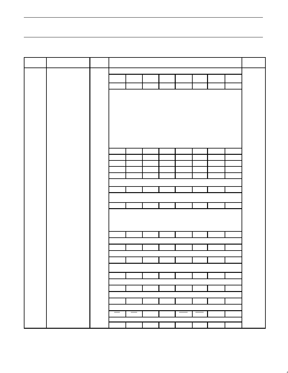
10
Table 1.
8XC52/54/58/80C32 Special Function Registers
SYMBOL
DESCRIPTION
DIRECT
ADDRESS
BIT ADDRESS, SYMBOL, OR ALTERNATIVE PORT FUNCTION
MSB
LSB
RESET
VALUE
ACC*
Accumulator
E0H
E7
E6
E5
E4
E3
E2
E1
E0
00H
AUXR#
Auxiliary
8EH
≠
≠
≠
≠
≠
≠
≠
AO
xxxxxxx0B
AUXR1#
Auxiliary 1
A2H
≠
≠
≠
LPEP
3
GF3
0
≠
DPS
xxx0xxx0B
B*
B register
F0H
F7
F6
F5
F4
F3
F2
F1
F0
00H
DPTR:
Data Pointer (2 bytes)
DPH
Data Pointer High
83H
00H
DPL
Data Pointer Low
82H
00H
AF
AE
AD
AC
AB
AA
A9
A8
IE*
Interrupt Enable
A8H
EA
≠
ET2
ES
ET1
EX1
ET0
EX0
0x000000B
BF
BE
BD
BC
BB
BA
B9
B8
IP*
Interrupt Priority
B8H
≠
≠
PT2
PS
PT1
PX1
PT0
PX0
xx000000B
B7
B6
B5
B4
B3
B2
B1
B0
IPH#
Interrupt Priority High
B7H
≠
≠
PT2H
PSH
PT1H
PX1H
PT0H
PX0H
xx000000B
87
86
85
84
83
82
81
80
P0*
Port 0
80H
AD7
AD6
AD5
AD4
AD3
AD2
AD1
AD0
FFH
97
96
95
94
93
92
91
90
P1*
Port 1
90H
≠
≠
≠
≠
≠
≠
T2EX
T2
FFH
A7
A6
A5
A4
A3
A2
A1
A0
P2*
Port 2
A0H
AD15
AD14
AD13
AD12
AD11
AD10
AD9
AD8
FFH
B7
B6
B5
B4
B3
B2
B1
B0
P3*
Port 3
B0H
RD
WR
T1
T0
INT1
INT0
TxD
RxD
FFH
PCON#
1
Power Control
87H
SMOD1
SMOD0
≠
POF
2
GF1
GF0
PD
IDL
00xx0000B
D7
D6
D5
D4
D3
D2
D1
D0
PSW*
Program Status Word
D0H
CY
AC
F0
RS1
RS0
OV
≠
P
000000x0B
RCAP2H
#
Timer 2 Capture High
CBH
00H
RCAP2L
#
Timer 2 Capture Low
CAH
00H
SADDR#
Slave Address
A9H
00H
SADEN#
Slave Address Mask
B9H
00H
SBUF
Serial Data Buffer
99H
xxxxxxxxB
9F
9E
9D
9C
9B
9A
99
98
SCON*
Serial Control
98H
SM0/FE
SM1
SM2
REN
TB8
RB8
TI
RI
00H
SP
Stack Pointer
81H
07H
8F
8E
8D
8C
8B
8A
89
88
TCON*
Timer Control
88H
TF1
TR1
TF0
TR0
IE1
IT1
IE0
IT0
00H
CF
CE
CD
CC
CB
CA
C9
C8
T2CON*
Timer 2 Control
C8H
TF2
EXF2
RCLK
TCLK
EXEN2
TR2
C/T2
CP/RL2
00H
T2MOD#
Timer 2 Mode Control
C9H
≠
≠
≠
≠
≠
≠
T2OE
DCEN
xxxxxx00B
TH0
Timer High 0
8CH
00H
TH1
Timer High 1
8DH
00H
TH2#
Timer High 2
CDH
00H
TL0
Timer Low 0
8AH
00H
TL1
Timer Low 1
8BH
00H
TL2#
Timer Low 2
CCH
00H
TMOD
Timer Mode
89H
GATE
C/T
M1
M0
GATE
C/T
M1
M0
00H
*
SFRs are bit addressable.
#
SFRs are modified from or added to the 80C51 SFRs.
≠
Reserved bits.
1. Reset value depends on reset source.
2. Bit will not be affected by Reset.
3. LPEP ≠ Low Power OTP≠EPROM only operation.
Philips Semiconductors
Product specification
8XC52/54/58/80C32
8XC51FA/FB/FC/80C51FA
8XC51RA+/RB+/RC+/RD+/80C51RA+
80C51 8-bit microcontroller family
8K≠64K/256≠1K OTP/ROM/ROMless, low voltage (2.7V≠5.5V),
low power, high speed (33MHz)
1999 Apr 01
11
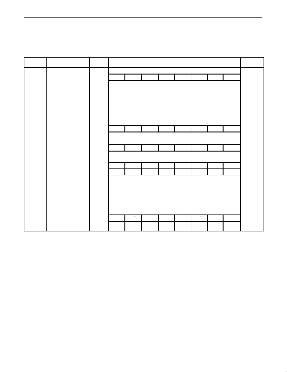
Table 2.
8XC51FA/FB/FC, 8XC51RA+/RB+/RC+/RD+ Special Function Registers
SYMBOL
DESCRIPTION
DIRECT
ADDRESS
BIT ADDRESS, SYMBOL, OR ALTERNATIVE PORT FUNCTION
MSB
LSB
RESET
VALUE
ACC*
Accumulator
E0H
E7
E6
E5
E4
E3
E2
E1
E0
00H
AUXR#
Auxiliary
8EH
≠
≠
≠
≠
≠
≠
EXTRAM
(RX+ only)
AO
xxxxxx00B
AUXR1#
Auxiliary 1
A2H
≠
≠
≠
LPEP
3
GF3
0
≠
DPS
xxx0xxx0B
B*
B register
F0H
F7
F6
F5
F4
F3
F2
F1
F0
00H
CCAP0H#
Module 0 Capture High
FAH
xxxxxxxxB
CCAP1H#
Module 1 Capture High
FBH
xxxxxxxxB
CCAP2H#
Module 2 Capture High
FCH
xxxxxxxxB
CCAP3H#
Module 3 Capture High
FDH
xxxxxxxxB
CCAP4H#
Module 4 Capture High
FEH
xxxxxxxxB
CCAP0L#
Module 0 Capture Low
EAH
xxxxxxxxB
CCAP1L#
Module 1 Capture Low
EBH
xxxxxxxxB
CCAP2L#
Module 2 Capture Low
ECH
xxxxxxxxB
CCAP3L#
Module 3 Capture Low
EDH
xxxxxxxxB
CCAP4L#
Module 4 Capture Low
EEH
xxxxxxxxB
CCAPM0#
Module 0 Mode
DAH
≠
ECOM
CAPP
CAPN
MAT
TOG
PWM
ECCF
x0000000B
CCAPM1#
Module 1 Mode
DBH
≠
ECOM
CAPP
CAPN
MAT
TOG
PWM
ECCF
x0000000B
CCAPM2#
Module 2 Mode
DCH
≠
ECOM
CAPP
CAPN
MAT
TOG
PWM
ECCF
x0000000B
CCAPM3#
Module 3 Mode
DDH
≠
ECOM
CAPP
CAPN
MAT
TOG
PWM
ECCF
x0000000B
CCAPM4#
Module 4 Mode
DEH
≠
ECOM
CAPP
CAPN
MAT
TOG
PWM
ECCF
x0000000B
DF
DE
DD
DC
DB
DA
D9
D8
CCON*#
PCA Counter Control
D8H
CF
CR
≠
CCF4
CCF3
CCF2
CCF1
CCF0
00x00000B
CH#
PCA Counter High
F9H
00H
CL#
PCA Counter Low
E9H
00H
CMOD#
PCA Counter Mode
D9H
CIDL
WDTE
≠
≠
≠
CPS1
CPS0
ECF
00xxx000B
DPTR:
Data Pointer (2 bytes)
DPH
Data Pointer High
83H
00H
DPL
Data Pointer Low
82H
00H
AF
AE
AD
AC
AB
AA
A9
A8
IE*
Interrupt Enable
A8H
EA
EC
ET2
ES
ET1
EX1
ET0
EX0
00H
BF
BE
BD
BC
BB
BA
B9
B8
IP*
Interrupt Priority
B8H
≠
PPC
PT2
PS
PT1
PX1
PT0
PX0
x0000000B
B7
B6
B5
B4
B3
B2
B1
B0
IPH#
Interrupt Priority High
B7H
≠
PPCH
PT2H
PSH
PT1H
PX1H
PT0H
PX0H
x0000000B
87
86
85
84
83
82
81
80
P0*
Port 0
80H
AD7
AD6
AD5
AD4
AD3
AD2
AD1
AD0
FFH
97
96
95
94
93
92
91
90
P1*
Port 1
90H
CEX4
CEX3
CEX2
CEX1
CEX0
ECI
T2EX
T2
FFH
A7
A6
A5
A4
A3
A2
A1
A0
P2*
Port 2
A0H
AD15
AD14
AD13
AD12
AD11
AD10
AD9
AD8
FFH
B7
B6
B5
B4
B3
B2
B1
B0
P3*
Port 3
B0H
RD
WR
T1
T0
INT1
INT0
TxD
RxD
FFH
PCON#
1
Power Control
87H
SMOD1
SMOD0
≠
POF
2
GF1
GF0
PD
IDL
00xx0000B
*
SFRs are bit addressable.
#
SFRs are modified from or added to the 80C51 SFRs.
≠
Reserved bits.
1. Reset value depends on reset source.
2. Bit will not be affected by Reset.
3. LPEP ≠ Low Power OTP≠EPROM only operation.
Philips Semiconductors
Product specification
8XC52/54/58/80C32
8XC51FA/FB/FC/80C51FA
8XC51RA+/RB+/RC+/RD+/80C51RA+
80C51 8-bit microcontroller family
8K≠64K/256≠1K OTP/ROM/ROMless, low voltage (2.7V≠5.5V),
low power, high speed (33MHz)
1999 Apr 01
12
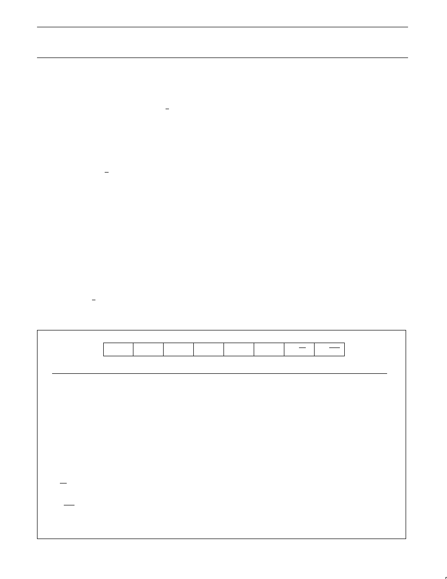
Table 2.
8XC51FA/FB/FC, 8XC51RA+/RB+/RC+/RD+ Special Function Registers (Continued)
SYMBOL
DESCRIPTION
DIRECT
ADDRESS
BIT ADDRESS, SYMBOL, OR ALTERNATIVE PORT FUNCTION
MSB
LSB
RESET
VALUE
D7
D6
D5
D4
D3
D2
D1
D0
PSW*
Program Status Word
D0H
CY
AC
F0
RS1
RS0
OV
≠
P
000000x0B
RACAP2H
#
Timer 2 Capture High
CBH
00H
RACAP2L
#
Timer 2 Capture Low
CAH
00H
SADDR#
Slave Address
A9H
00H
SADEN#
Slave Address Mask
B9H
00H
SBUF
Serial Data Buffer
99H
xxxxxxxxB
9F
9E
9D
9C
9B
9A
99
98
SCON*
Serial Control
98H
SM0/FE
SM1
SM2
REN
TB8
RB8
TI
RI
00H
SP
Stack Pointer
81H
07H
8F
8E
8D
8C
8B
8A
89
88
TCON*
Timer Control
88H
TF1
TR1
TF0
TR0
IE1
IT1
IE0
IT0
00H
CF
CE
CD
CC
CB
CA
C9
C8
T2CON*
Timer 2 Control
C8H
TF2
EXF2
RCLK
TCLK
EXEN2
TR2
C/T2
CP/RL2
00H
T2MOD#
Timer 2 Mode Control
C9H
≠
≠
≠
≠
≠
≠
T2OE
DCEN
xxxxxx00B
TH0
Timer High 0
8CH
00H
TH1
Timer High 1
8DH
00H
TH2#
Timer High 2
CDH
00H
TL0
Timer Low 0
8AH
00H
TL1
Timer Low 1
8BH
00H
TL2#
Timer Low 2
CCH
00H
TMOD
Timer Mode
89H
GATE
C/T
M1
M0
GATE
C/T
M1
M0
00H
WDTRST
HDW Watchdog
Timer Reset (RX+ only)
0A6H
*
SFRs are bit addressable.
#
SFRs are modified from or added to the 80C51 SFRs.
≠
Reserved bits.
OSCILLATOR CHARACTERISTICS
XTAL1 and XTAL2 are the input and output, respectively, of an
inverting amplifier. The pins can be configured for use as an on-chip
oscillator.
To drive the device from an external clock source, XTAL1 should be
driven while XTAL2 is left unconnected. There are no requirements
on the duty cycle of the external clock signal, because the input to
the internal clock circuitry is through a divide-by-two flip-flop.
However, minimum and maximum high and low times specified in
the data sheet must be observed.
RESET
A reset is accomplished by holding the RST pin high for at least two
machine cycles (24 oscillator periods), while the oscillator is running.
To insure a good power-on reset, the RST pin must be high long
enough to allow the oscillator time to start up (normally a few
milliseconds) plus two machine cycles. At power-on, the voltage on
V
CC
and RST must come up at the same time for a proper start-up.
Ports 1, 2, and 3 will asynchronously be driven to their reset
condition when a voltage above V
IH1
(min.) is applied to RESET.

Philips Semiconductors
Product specification
8XC52/54/58/80C32
8XC51FA/FB/FC/80C51FA
8XC51RA+/RB+/RC+/RD+/80C51RA+
80C51 8-bit microcontroller family
8K≠64K/256≠1K OTP/ROM/ROMless, low voltage (2.7V≠5.5V),
low power, high speed (33MHz)
1999 Apr 01
13
LOW POWER MODES
Stop Clock Mode
The static design enables the clock speed to be reduced down to
0 MHz (stopped). When the oscillator is stopped, the RAM and
Special Function Registers retain their values. This mode allows
step-by-step utilization and permits reduced system power
consumption by lowering the clock frequency down to any value. For
lowest power consumption the Power Down mode is suggested.
Idle Mode
In the idle mode (see Table 3), the CPU puts itself to sleep while all
of the on-chip peripherals stay active. The instruction to invoke the
idle mode is the last instruction executed in the normal operating
mode before the idle mode is activated. The CPU contents, the
on-chip RAM, and all of the special function registers remain intact
during this mode. The idle mode can be terminated either by any
enabled interrupt (at which time the process is picked up at the
interrupt service routine and continued), or by a hardware reset
which starts the processor in the same manner as a power-on reset.
Power-Down Mode
To save even more power, a Power Down mode (see Table 3) can
be invoked by software. In this mode, the oscillator is stopped and
the instruction that invoked Power Down is the last instruction
executed. The on-chip RAM and Special Function Registers retain
their values down to 2.0V and care must be taken to return V
CC
to
the minimum specified operating voltages before the Power Down
Mode is terminated.
Either a hardware reset or external interrupt can be used to exit from
Power Down. Reset redefines all the SFRs but does not change the
on-chip RAM. An external interrupt allows both the SFRs and the
on-chip RAM to retain their values.
To properly terminate Power Down the reset or external interrupt
should not be executed before V
CC
is restored to its normal
operating level and must be held active long enough for the
oscillator to restart and stabilize (normally less than 10ms).
With an external interrupt, INT0 and INT1 must be enabled and
configured as level-sensitive. Holding the pin low restarts the oscillator
but bringing the pin back high completes the exit. Once the interrupt
is serviced, the next instruction to be executed after RETI will be the
one following the instruction that put the device into Power Down.
LPEP
The LPEP bit (AUXR.4), only needs to be set for applications
operating at V
CC
less than 4V.
POWER OFF FLAG
The Power Off Flag (POF) is set by on-chip circuitry when the V
CC
level on the 8XC51FX/8XC51RX+ rises from 0 to 5V. The POF bit
can be set or cleared by software allowing a user to determine if the
reset is the result of a power-on or a warm start after powerdown.
The V
CC
level must remain above 3V for the POF to remain
unaffected by the V
CC
level.
Design Consideration
∑
When the idle mode is terminated by a hardware reset, the device
normally resumes program execution, from where it left off, up to
two machine cycles before the internal reset algorithm takes
control. On-chip hardware inhibits access to internal RAM in this
event, but access to the port pins is not inhibited. To eliminate the
possibility of an unexpected write when Idle is terminated by reset,
the instruction following the one that invokes Idle should not be
one that writes to a port pin or to external memory.
ONCE
TM
Mode
The ONCE ("On-Circuit Emulation") Mode facilitates testing and
debugging of systems without the device having to be removed from
the circuit. The ONCE Mode is invoked by:
1. Pull ALE low while the device is in reset and PSEN is high;
2. Hold ALE low as RST is deactivated.
While the device is in ONCE Mode, the Port 0 pins go into a float
state, and the other port pins and ALE and PSEN are weakly pulled
high. The oscillator circuit remains active. While the device is in this
mode, an emulator or test CPU can be used to drive the circuit.
Normal operation is restored when a normal reset is applied.
Programmable Clock-Out
A 50% duty cycle clock can be programmed to come out on P1.0.
This pin, besides being a regular I/O pin, has two alternate
functions. It can be programmed:
1. to input the external clock for Timer/Counter 2, or
2. to output a 50% duty cycle clock ranging from 61Hz to 4MHz at a
16MHz operating frequency.
To configure the Timer/Counter 2 as a clock generator, bit C/T2 (in
T2CON) must be cleared and bit T20E in T2MOD must be set. Bit
TR2 (T2CON.2) also must be set to start the timer.
The Clock-Out frequency depends on the oscillator frequency and
the reload value of Timer 2 capture registers (RCAP2H, RCAP2L)
as shown in this equation:
Oscillator Frequency
4
(65536
*
RCAP2H, RCAP2L)
Where (RCAP2H,RCAP2L) = the content of RCAP2H and RCAP2L
taken as a 16-bit unsigned integer.
In the Clock-Out mode Timer 2 roll-overs will not generate an
interrupt. This is similar to when it is used as a baud-rate generator.
It is possible to use Timer 2 as a baud-rate generator and a clock
generator simultaneously. Note, however, that the baud-rate and the
Clock-Out frequency will be the same.
Table 3. External Pin Status During Idle and Power-Down Mode
MODE
PROGRAM MEMORY
ALE
PSEN
PORT 0
PORT 1
PORT 2
PORT 3
Idle
Internal
1
1
Data
Data
Data
Data
Idle
External
1
1
Float
Data
Address
Data
Power-down
Internal
0
0
Data
Data
Data
Data
Power-down
External
0
0
Float
Data
Data
Data
Philips Semiconductors
Product specification
8XC52/54/58/80C32
8XC51FA/FB/FC/80C51FA
8XC51RA+/RB+/RC+/RD+/80C51RA+
80C51 8-bit microcontroller family
8K≠64K/256≠1K OTP/ROM/ROMless, low voltage (2.7V≠5.5V),
low power, high speed (33MHz)
1999 Apr 01
14
TIMER 2 OPERATION
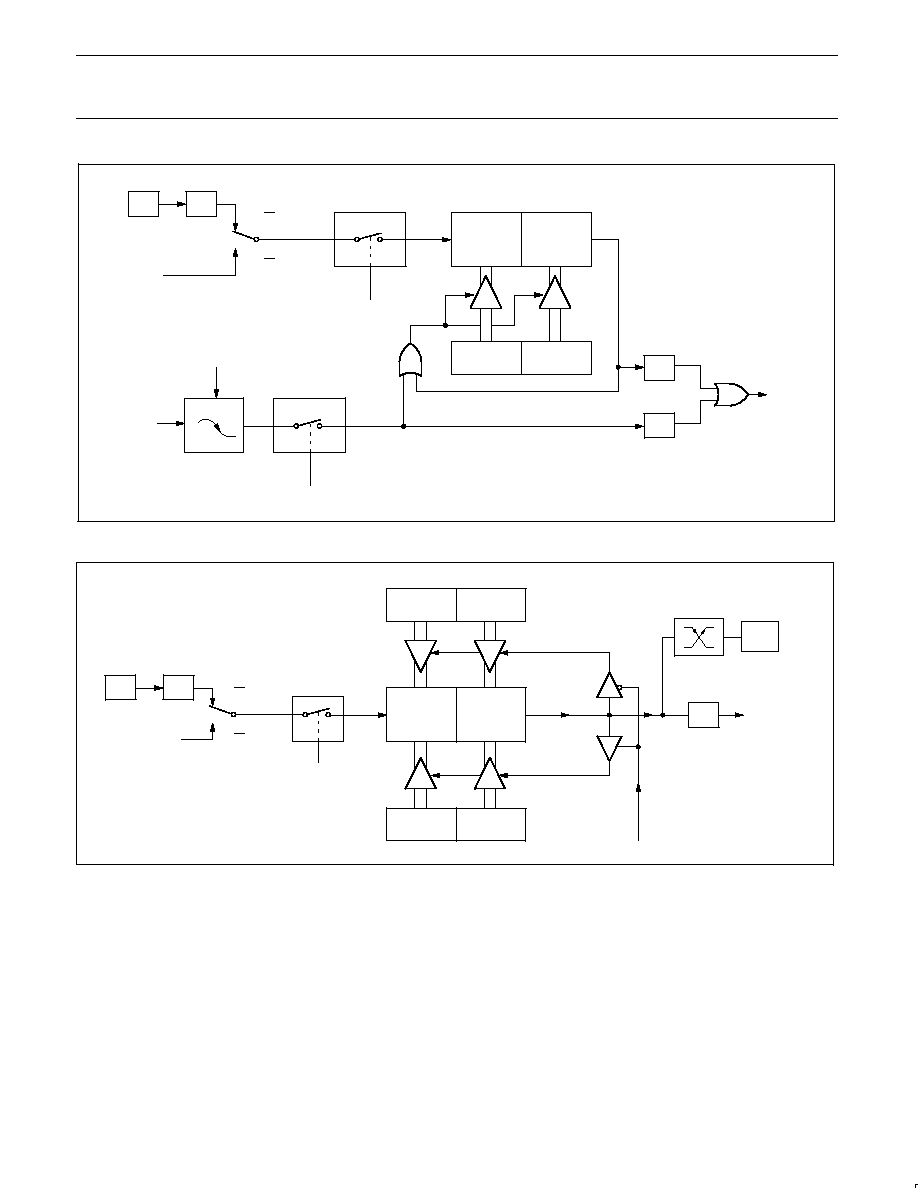
Timer 2
Timer 2 is a 16-bit Timer/Counter which can operate as either an
event timer or an event counter, as selected by C/T2* in the special
function register T2CON (see Figure 1). Timer 2 has three operating
modes: Capture, Auto-reload (up or down counting), and Baud Rate
Generator, which are selected by bits in the T2CON as shown in
Table 4.
Capture Mode
In the capture mode there are two options which are selected by bit
EXEN2 in T2CON. If EXEN2=0, then timer 2 is a 16-bit timer or
counter (as selected by C/T2* in T2CON) which, upon overflowing
sets bit TF2, the timer 2 overflow bit. This bit can be used to
generate an interrupt (by enabling the Timer 2 interrupt bit in the
IE register). If EXEN2= 1, Timer 2 operates as described above, but
with the added feature that a 1-to-0 transition at external input T2EX
causes the current value in the Timer 2 registers, TL2 and TH2, to
be captured into registers RCAP2L and RCAP2H, respectively. In
addition, the transition at T2EX causes bit EXF2 in T2CON to be
set, and EXF2 like TF2 can generate an interrupt (which vectors to
the same location as Timer 2 overflow interrupt. The Timer 2
interrupt service routine can interrogate TF2 and EXF2 to determine
which event caused the interrupt). The capture mode is illustrated in
Figure 2. (There is no reload value for TL2 and TH2 in this mode.
Even when a capture event occurs from T2EX, the counter keeps on
counting T2EX pin transitions or osc/12 pulses.)
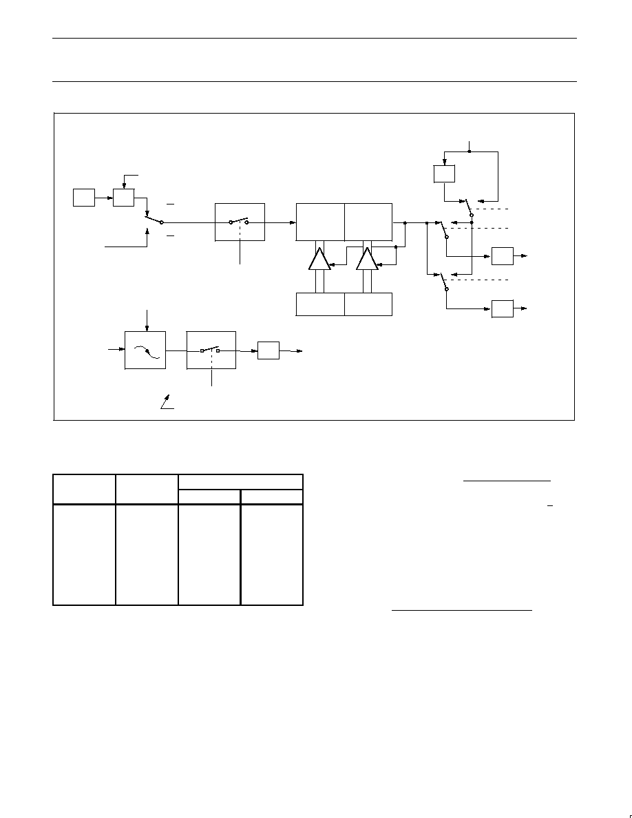
Auto-Reload Mode (Up or Down Counter)
In the 16-bit auto-reload mode, Timer 2 can be configured (as either
a timer or counter [C/T2* in T2CON]) then programmed to count up
or down. The counting direction is determined by bit DCEN (Down
Counter Enable) which is located in the T2MOD register (see
Figure 3). When reset is applied the DCEN=0 which means Timer 2
will default to counting up. If DCEN bit is set, Timer 2 can count up
or down depending on the value of the T2EX pin.
Figure 4 shows Timer 2 which will count up automatically since
DCEN=0. In this mode there are two options selected by bit EXEN2
in T2CON register. If EXEN2=0, then Timer 2 counts up to 0FFFFH
and sets the TF2 (Overflow Flag) bit upon overflow. This causes the
Timer 2 registers to be reloaded with the 16-bit value in RCAP2L
and RCAP2H. The values in RCAP2L and RCAP2H are preset by
software means.
If EXEN2=1, then a 16-bit reload can be triggered either by an
overflow or by a 1-to-0 transition at input T2EX. This transition also
sets the EXF2 bit. The Timer 2 interrupt, if enabled, can be
generated when either TF2 or EXF2 are 1.
In Figure 5 DCEN=1, which enables Timer 2 to count up or down.
This mode allows pin T2EX to control the direction of count. When a
logic 1 is applied at pin T2EX Timer 2 will count up. Timer 2 will
overflow at 0FFFFH and set the TF2 flag, which can then generate
an interrupt, if the interrupt is enabled. This timer overflow also
causes the 16≠bit value in RCAP2L and RCAP2H to be reloaded
into the timer registers TL2 and TH2.
When a logic 0 is applied at pin T2EX this causes Timer 2 to count
down. The timer will underflow when TL2 and TH2 become equal to
the value stored in RCAP2L and RCAP2H. Timer 2 underflow sets
the TF2 flag and causes 0FFFFH to be reloaded into the timer
registers TL2 and TH2.
The external flag EXF2 toggles when Timer 2 underflows or
overflows. This EXF2 bit can be used as a 17th bit of resolution if
needed. The EXF2 flag does not generate an interrupt in this mode
of operation.
(MSB)
(LSB)
Symbol
Position
Name and Significance
TF2
T2CON.7
Timer 2 overflow flag set by a Timer 2 overflow and must be cleared by software. TF2 will not be set
when either RCLK or TCLK = 1.
EXF2
T2CON.6
Timer 2 external flag set when either a capture or reload is caused by a negative transition on T2EX and
EXEN2 = 1. When Timer 2 interrupt is enabled, EXF2 = 1 will cause the CPU to vector to the Timer 2
interrupt routine. EXF2 must be cleared by software. EXF2 does not cause an interrupt in up/down
counter mode (DCEN = 1).
RCLK
T2CON.5
Receive clock flag. When set, causes the serial port to use Timer 2 overflow pulses for its receive clock
in modes 1 and 3. RCLK = 0 causes Timer 1 overflow to be used for the receive clock.
TCLK
T2CON.4
Transmit clock flag. When set, causes the serial port to use Timer 2 overflow pulses for its transmit clock
in modes 1 and 3. TCLK = 0 causes Timer 1 overflows to be used for the transmit clock.
EXEN2
T2CON.3
Timer 2 external enable flag. When set, allows a capture or reload to occur as a result of a negative
transition on T2EX if Timer 2 is not being used to clock the serial port. EXEN2 = 0 causes Timer 2 to
ignore events at T2EX.
TR2
T2CON.2
Start/stop control for Timer 2. A logic 1 starts the timer.
C/T2
T2CON.1
Timer or counter select. (Timer 2)
0 = Internal timer (OSC/12)
1 = External event counter (falling edge triggered).
CP/RL2
T2CON.0
Capture/Reload flag. When set, captures will occur on negative transitions at T2EX if EXEN2 = 1. When
cleared, auto-reloads will occur either with Timer 2 overflows or negative transitions at T2EX when
EXEN2 = 1. When either RCLK = 1 or TCLK = 1, this bit is ignored and the timer is forced to auto-reload
on Timer 2 overflow.
TF2
EXF2
RCLK
TCLK
EXEN2
TR2
C/T2
CP/RL2
SU00728
Figure 1. Timer/Counter 2 (T2CON) Control Register
Philips Semiconductors
Product specification
8XC52/54/58/80C32
8XC51FA/FB/FC/80C51FA
8XC51RA+/RB+/RC+/RD+/80C51RA+
80C51 8-bit microcontroller family
8K≠64K/256≠1K OTP/ROM/ROMless, low voltage (2.7V≠5.5V),
low power, high speed (33MHz)
1999 Apr 01
15
Table 4. Timer 2 Operating Modes
RCLK + TCLK
CP/RL2
TR2
MODE
0
0
1
16-bit Auto-reload
0
1
1
16-bit Capture
1
X
1
Baud rate generator
X
X
0
(off)
OSC
˜
12
C/T2 = 0
C/T2 = 1
TR2
Control
TL2
(8-bits)
TH2
(8-bits)
TF2
RCAP2L
RCAP2H
EXEN2
Control
EXF2
Timer 2
Interrupt
T2EX Pin
Transition
Detector
T2 Pin
Capture
SU00066
Figure 2. Timer 2 in Capture Mode
Not Bit Addressable
Symbol
Function
--
Not implemented, reserved for future use.*
T2OE
Timer 2 Output Enable bit.
DCEN
Down Count Enable bit. When set, this allows Timer 2 to be configured as an up/down counter.
--
--
--
--
--
--
T2OE
DCEN
SU00729
7
6
5
4
3
2
1
0
*
User software should not write 1s to reserved bits. These bits may be used in future 8051 family products to invoke new features.
In that case, the reset or inactive value of the new bit will be 0, and its active value will be 1. The value read from a reserved bit is
indeterminate.
Bit
T2MOD
Address = 0C9H
Reset Value = XXXX XX00B
Figure 3. Timer 2 Mode (T2MOD) Control Register
Philips Semiconductors
Product specification
8XC52/54/58/80C32
8XC51FA/FB/FC/80C51FA
8XC51RA+/RB+/RC+/RD+/80C51RA+
80C51 8-bit microcontroller family
8K≠64K/256≠1K OTP/ROM/ROMless, low voltage (2.7V≠5.5V),
low power, high speed (33MHz)
1999 Apr 01
16
OSC
˜
12
C/T2 = 0
C/T2 = 1
TR2
CONTROL
TL2
(8-BITS)
TH2
(8-BITS)
TF2
RCAP2L
RCAP2H
EXEN2
CONTROL
EXF2
TIMER 2
INTERRUPT
T2EX PIN
TRANSITION
DETECTOR
T2 PIN
RELOAD
SU00067
Figure 4. Timer 2 in Auto-Reload Mode (DCEN = 0)
˜
12
C/T2 = 0
C/T2 = 1
TL2
TH2
TR2
CONTROL
T2 PIN
SU00730
FFH
FFH
RCAP2L
RCAP2H
(UP COUNTING RELOAD VALUE)
T2EX PIN
TF2
INTERRUPT
COUNT
DIRECTION
1 = UP
0 = DOWN
EXF2
OVERFLOW
(DOWN COUNTING RELOAD VALUE)
TOGGLE
OSC
Figure 5. Timer 2 Auto Reload Mode (DCEN = 1)
Philips Semiconductors
Product specification
8XC52/54/58/80C32
8XC51FA/FB/FC/80C51FA
8XC51RA+/RB+/RC+/RD+/80C51RA+
80C51 8-bit microcontroller family
8K≠64K/256≠1K OTP/ROM/ROMless, low voltage (2.7V≠5.5V),
low power, high speed (33MHz)
1999 Apr 01
17
OSC
˜
2
C/T2 = 0
C/T2 = 1
TR2
Control
TL2
(8-bits)
TH2
(8-bits)
˜
16
RCAP2L
RCAP2H
EXEN2
Control
EXF2
Timer 2
Interrupt
T2EX Pin
Transition
Detector
T2 Pin
Reload
NOTE: OSC. Freq. is divided by 2, not 12.
˜
2
"0"
"1"
RX Clock
˜
16
TX Clock
"0"
"1"
"0"
"1"
Timer 1
Overflow
Note availability of additional external interrupt.
SMOD
RCLK
TCLK
SU00068
Figure 6. Timer 2 in Baud Rate Generator Mode
Table 5. Timer 2 Generated Commonly Used
Baud Rates
Ba d Rate
Osc Freq
Timer 2
Baud Rate
Osc Freq
RCAP2H
RCAP2L
375K
12MHz
FF
FF
9.6K
12MHz
FF
D9
2.8K
12MHz
FF
B2
2.4K
12MHz
FF
64
1.2K
12MHz
FE
C8
300
12MHz
FB
1E
110
12MHz
F2
AF
300
6MHz
FD
8F
110
6MHz
F9
57
Baud Rate Generator Mode
Bits TCLK and/or RCLK in T2CON (Table 5) allow the serial port
transmit and receive baud rates to be derived from either Timer 1 or
Timer 2. When TCLK= 0, Timer 1 is used as the serial port transmit
baud rate generator. When TCLK= 1, Timer 2 is used as the serial
port transmit baud rate generator. RCLK has the same effect for the
serial port receive baud rate. With these two bits, the serial port can
have different receive and transmit baud rates ≠ one generated by
Timer 1, the other by Timer 2.
Figure 6 shows the Timer 2 in baud rate generation mode. The baud
rate generation mode is like the auto-reload mode,in that a rollover
in TH2 causes the Timer 2 registers to be reloaded with the 16-bit
value in registers RCAP2H and RCAP2L, which are preset by
software.
The baud rates in modes 1 and 3 are determined by Timer 2's
overflow rate given below:
Modes 1 and 3 Baud Rates
+
Timer 2 Overflow Rate
16
The timer can be configured for either "timer" or "counter" operation.
In many applications, it is configured for "timer" operation (C/T2*=0).
Timer operation is different for Timer 2 when it is being used as a
baud rate generator.
Usually, as a timer it would increment every machine cycle (i.e., 1/12
the oscillator frequency). As a baud rate generator, it increments
every state time (i.e., 1/2 the oscillator frequency). Thus the baud
rate formula is as follows:
Oscillator Frequency
[32
[65536
*
(RCAP2H, RCAP2L)]]
Modes 1 and 3 Baud Rates =
Where:
(RCAP2H, RCAP2L)= The content of RCAP2H and
RCAP2L taken as a 16-bit unsigned integer.
The Timer 2 as a baud rate generator mode shown in Figure 6, is
valid only if RCLK and/or TCLK = 1 in T2CON register. Note that a
rollover in TH2 does not set TF2, and will not generate an interrupt.
Thus, the Timer 2 interrupt does not have to be disabled when
Timer 2 is in the baud rate generator mode. Also if the EXEN2
(T2 external enable flag) is set, a 1-to-0 transition in T2EX
(Timer/counter 2 trigger input) will set EXF2 (T2 external flag) but
will not cause a reload from (RCAP2H, RCAP2L) to (TH2,TL2).
Therefore when Timer 2 is in use as a baud rate generator, T2EX
can be used as an additional external interrupt, if needed.
Philips Semiconductors
Product specification
8XC52/54/58/80C32
8XC51FA/FB/FC/80C51FA
8XC51RA+/RB+/RC+/RD+/80C51RA+
80C51 8-bit microcontroller family
8K≠64K/256≠1K OTP/ROM/ROMless, low voltage (2.7V≠5.5V),
low power, high speed (33MHz)
1999 Apr 01
18
When Timer 2 is in the baud rate generator mode, one should not try
to read or write TH2 and TL2. As a baud rate generator, Timer 2 is
incremented every state time (osc/2) or asynchronously from pin T2;
under these conditions, a read or write of TH2 or TL2 may not be
accurate. The RCAP2 registers may be read, but should not be
written to, because a write might overlap a reload and cause write
and/or reload errors. The timer should be turned off (clear TR2)
before accessing the Timer 2 or RCAP2 registers.
Table 5 shows commonly used baud rates and how they can be
obtained from Timer 2.
Summary Of Baud Rate Equations
Timer 2 is in baud rate generating mode. If Timer 2 is being clocked
through pin T2(P1.0) the baud rate is:
Baud Rate
+
Timer 2 Overflow Rate
16
If Timer 2 is being clocked internally , the baud rate is:
Baud Rate
+
f
OSC
[32
[65536
*
(RCAP2H, RCAP2L)]]
Where f
OSC
= Oscillator Frequency
To obtain the reload value for RCAP2H and RCAP2L, the above
equation can be rewritten as:
RCAP2H, RCAP2L
+
65536
*
f
OSC
32
Baud Rate
Timer/Counter 2 Set-up
Except for the baud rate generator mode, the values given for
T2CON do not include the setting of the TR2 bit. Therefore, bit TR2
must be set, separately, to turn the timer on. See Table 6 for set-up
of Timer 2 as a timer. Also see Table 7 for set-up of Timer 2 as a
counter.
Table 6. Timer 2 as a Timer
T2CON
MODE
INTERNAL CONTROL
(Note 1)
EXTERNAL CONTROL
(Note 2)
16-bit Auto-Reload
00H
08H
16-bit Capture
01H
09H
Baud rate generator receive and transmit same baud rate
34H
36H
Receive only
24H
26H
Transmit only
14H
16H
Table 7. Timer 2 as a Counter
TMOD
MODE
INTERNAL CONTROL
(Note 1)
EXTERNAL CONTROL
(Note 2)
16-bit
02H
0AH
Auto-Reload
03H
0BH
NOTES:
1. Capture/reload occurs only on timer/counter overflow.
2. Capture/reload occurs on timer/counter overflow and a 1-to-0 transition on T2EX (P1.1) pin except when Timer 2 is used in the baud rate
generator mode.

Philips Semiconductors
Product specification
8XC52/54/58/80C32
8XC51FA/FB/FC/80C51FA
8XC51RA+/RB+/RC+/RD+/80C51RA+
80C51 8-bit microcontroller family
8K≠64K/256≠1K OTP/ROM/ROMless, low voltage (2.7V≠5.5V),
low power, high speed (33MHz)
1999 Apr 01
19
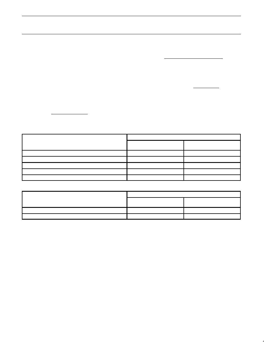
Enhanced UART
The UART operates in all of the usual modes that are described in
the first section of
Data Handbook IC20, 80C51-Based 8-Bit
Microcontrollers. In addition the UART can perform framing error
detect by looking for missing stop bits, and automatic address
recognition. The UART also fully supports multiprocessor
communication as does the standard 80C51 UART.
When used for framing error detect the UART looks for missing stop
bits in the communication. A missing bit will set the FE bit in the
SCON register. The FE bit shares the SCON.7 bit with SM0 and the
function of SCON.7 is determined by PCON.6 (SMOD0) (see
Figure 7). If SMOD0 is set then SCON.7 functions as FE. SCON.7
functions as SM0 when SMOD0 is cleared. When used as FE
SCON.7 can only be cleared by software. Refer to Figure 8.
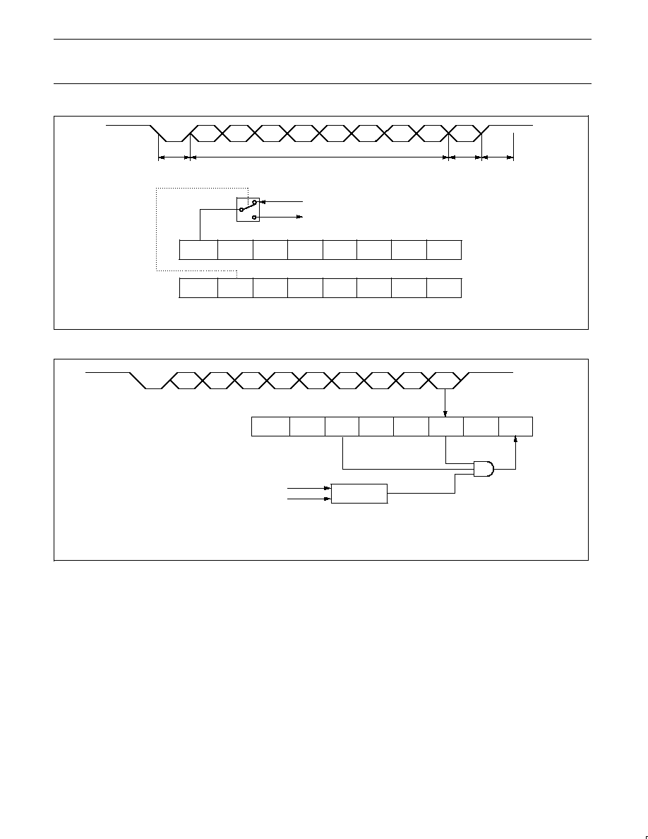
Automatic Address Recognition
Automatic Address Recognition is a feature which allows the UART
to recognize certain addresses in the serial bit stream by using
hardware to make the comparisons. This feature saves a great deal
of software overhead by eliminating the need for the software to
examine every serial address which passes by the serial port. This
feature is enabled by setting the SM2 bit in SCON. In the 9 bit UART
modes, mode 2 and mode 3, the Receive Interrupt flag (RI) will be
automatically set when the received byte contains either the "Given"
address or the "Broadcast" address. The 9 bit mode requires that
the 9th information bit is a 1 to indicate that the received information
is an address and not data. Automatic address recognition is shown
in Figure 9.
The 8 bit mode is called Mode 1. In this mode the RI flag will be set
if SM2 is enabled and the information received has a valid stop bit
following the 8 address bits and the information is either a Given or
Broadcast address.
Mode 0 is the Shift Register mode and SM2 is ignored.
Using the Automatic Address Recognition feature allows a master to
selectively communicate with one or more slaves by invoking the
Given slave address or addresses. All of the slaves may be
contacted by using the Broadcast address. Two special Function
Registers are used to define the slave's address, SADDR, and the
address mask, SADEN. SADEN is used to define which bits in the
SADDR are to b used and which bits are "don't care". The SADEN
mask can be logically ANDed with the SADDR to create the "Given"
address which the master will use for addressing each of the slaves.
Use of the Given address allows multiple slaves to be recognized
while excluding others. The following examples will help to show the
versatility of this scheme:
Slave 0
SADDR
=
1100 0000
SADEN
=
1111 1101
Given
=
1100 00X0
Slave 1
SADDR
=
1100 0000
SADEN
=
1111 1110
Given
=
1100 000X
In the above example SADDR is the same and the SADEN data is
used to differentiate between the two slaves. Slave 0 requires a 0 in
bit 0 and it ignores bit 1. Slave 1 requires a 0 in bit 1 and bit 0 is
ignored. A unique address for Slave 0 would be 1100 0010 since
slave 1 requires a 0 in bit 1. A unique address for slave 1 would be
1100 0001 since a 1 in bit 0 will exclude slave 0. Both slaves can be
selected at the same time by an address which has bit 0 = 0 (for
slave 0) and bit 1 = 0 (for slave 1). Thus, both could be addressed
with 1100 0000.
In a more complex system the following could be used to select
slaves 1 and 2 while excluding slave 0:
Slave 0
SADDR
=
1100 0000
SADEN
=
1111 1001
Given
=
1100 0XX0
Slave 1
SADDR
=
1110 0000
SADEN
=
1111 1010
Given
=
1110 0X0X
Slave 2
SADDR
=
1110 0000
SADEN
=
1111 1100
Given
=
1110 00XX
In the above example the differentiation among the 3 slaves is in the
lower 3 address bits. Slave 0 requires that bit 0 = 0 and it can be
uniquely addressed by 1110 0110. Slave 1 requires that bit 1 = 0 and
it can be uniquely addressed by 1110 and 0101. Slave 2 requires
that bit 2 = 0 and its unique address is 1110 0011. To select Slaves 0
and 1 and exclude Slave 2 use address 1110 0100, since it is
necessary to make bit 2 = 1 to exclude slave 2.
The Broadcast Address for each slave is created by taking the
logical OR of SADDR and SADEN. Zeros in this result are trended
as don't-cares. In most cases, interpreting the don't-cares as ones,
the broadcast address will be FF hexadecimal.
Upon reset SADDR (SFR address 0A9H) and SADEN (SFR
address 0B9H) are leaded with 0s. This produces a given address
of all "don't cares" as well as a Broadcast address of all "don't
cares". This effectively disables the Automatic Addressing mode and
allows the microcontroller to use standard 80C51 type UART drivers
which do not make use of this feature.

Philips Semiconductors
Product specification
8XC52/54/58/80C32
8XC51FA/FB/FC/80C51FA
8XC51RA+/RB+/RC+/RD+/80C51RA+
80C51 8-bit microcontroller family
8K≠64K/256≠1K OTP/ROM/ROMless, low voltage (2.7V≠5.5V),
low power, high speed (33MHz)
1999 Apr 01
20
SCON Address = 98H
Reset Value = 0000 0000B
SM0/FE
SM1
SM2
REN
TB8
RB8
Tl
Rl
Bit Addressable
(SMOD0 = 0/1)*
Symbol
Function
FE
Framing Error bit. This bit is set by the receiver when an invalid stop bit is detected. The FE bit is not cleared by valid
frames but should be cleared by software. The SMOD0 bit must be set to enable access to the FE bit.
SM0
Serial Port Mode Bit 0, (SMOD0 must = 0 to access bit SM0)
SM1
Serial Port Mode Bit 1
SM0
SM1
Mode
Description
Baud Rate**
0
0
0
shift register
f
OSC
/12
0
1
1
8-bit UART
variable
1
0
2
9-bit UART
f
OSC
/64 or f
OSC
/32
1
1
3
9-bit UART
variable
SM2
Enables the Automatic Address Recognition feature in Modes 2 or 3. If SM2 = 1 then Rl will not be set unless the
received 9th data bit (RB8) is 1, indicating an address, and the received byte is a Given or Broadcast Address.
In Mode 1, if SM2 = 1 then Rl will not be activated unless a valid stop bit was received, and the received byte is a
Given or Broadcast Address. In Mode 0, SM2 should be 0.
REN
Enables serial reception. Set by software to enable reception. Clear by software to disable reception.
TB8
The 9th data bit that will be transmitted in Modes 2 and 3. Set or clear by software as desired.
RB8
In modes 2 and 3, the 9th data bit that was received. In Mode 1, if SM2 = 0, RB8 is the stop bit that was received.
In Mode 0, RB8 is not used.
Tl
Transmit interrupt flag. Set by hardware at the end of the 8th bit time in Mode 0, or at the beginning of the stop bit in the
other modes, in any serial transmission. Must be cleared by software.
Rl
Receive interrupt flag. Set by hardware at the end of the 8th bit time in Mode 0, or halfway through the stop bit time in
the other modes, in any serial reception (except see SM2). Must be cleared by software.
NOTE:
*SMOD0 is located at PCON6.
**f
OSC
= oscillator frequency
SU00043
Bit:
7
6
5
4
3
2
1
0
Figure 7. SCON: Serial Port Control Register
Philips Semiconductors
Product specification
8XC52/54/58/80C32
8XC51FA/FB/FC/80C51FA
8XC51RA+/RB+/RC+/RD+/80C51RA+
80C51 8-bit microcontroller family
8K≠64K/256≠1K OTP/ROM/ROMless, low voltage (2.7V≠5.5V),
low power, high speed (33MHz)
1999 Apr 01
21
SMOD1
SMOD0
≠
POF
GF1
GF0
PD
IDL
PCON
(87H)
SM0 / FE
SM1
SM2
REN
TB8
RB8
TI
RI
SCON
(98H)
D0
D1
D2
D3
D4
D5
D6
D7
D8
STOP
BIT
DATA BYTE
ONLY IN
MODE 2, 3
START
BIT
SET FE BIT IF STOP BIT IS 0 (FRAMING ERROR)
SM0 TO UART MODE CONTROL
0 : SCON.7 = SM0
1 : SCON.7 = FE
SU01191
Figure 8. UART Framing Error Detection
SM0
SM1
SM2
REN
TB8
RB8
TI
RI
SCON
(98H)
D0
D1
D2
D3
D4
D5
D6
D7
D8
1
1
1
0
COMPARATOR
1
1
X
RECEIVED ADDRESS D0 TO D7
PROGRAMMED ADDRESS
IN UART MODE 2 OR MODE 3 AND SM2 = 1:
INTERRUPT IF REN=1, RB8=1 AND "RECEIVED ADDRESS" = "PROGRAMMED ADDRESS"
≠ WHEN OWN ADDRESS RECEIVED, CLEAR SM2 TO RECEIVE DATA BYTES
≠ WHEN ALL DATA BYTES HAVE BEEN RECEIVED: SET SM2 TO WAIT FOR NEXT ADDRESS.
SU00045
Figure 9. UART Multiprocessor Communication, Automatic Address Recognition
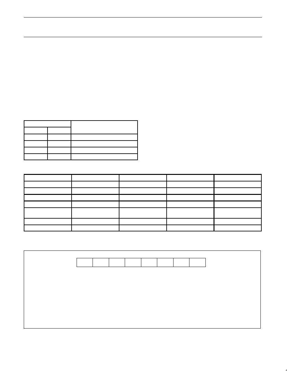
Philips Semiconductors
Product specification
8XC52/54/58/80C32
8XC51FA/FB/FC/80C51FA
8XC51RA+/RB+/RC+/RD+/80C51RA+
80C51 8-bit microcontroller family
8K≠64K/256≠1K OTP/ROM/ROMless, low voltage (2.7V≠5.5V),
low power, high speed (33MHz)
1999 Apr 01
22
Interrupt Priority Structure
The 8XC51FA/FB/FC and 8XC51RA+/RB+/RC+/RD+ have a
7-source four-level interrupt structure (see Table 8). The
80C52/54/58 and 80C32 only have a 6-source four-level interrupt
structure because these devices do not have a PCA.
There are 3 SFRs associated with the four-level interrupt. They are
the IE, IP, and IPH. (See Figures 10, 11, and 12.) The IPH (Interrupt
Priority High) register makes the four-level interrupt structure
possible. The IPH is located at SFR address B7H. The structure of
the IPH register and a description of its bits is shown in Figure 12.
The function of the IPH SFR is simple and when combined with the
IP SFR determines the priority of each interrupt. The priority of each
interrupt is determined as shown in the following table:
PRIORITY BITS
INTERRUPT PRIORITY LEVEL
IPH.x
IP.x
INTERRUPT PRIORITY LEVEL
0
0
Level 0 (lowest priority)
0
1
Level 1
1
0
Level 2
1
1
Level 3 (highest priority)
The priority scheme for servicing the interrupts is the same as that
for the 80C51, except there are four interrupt levels rather than two
as on the 80C51. An interrupt will be serviced as long as an interrupt
of equal or higher priority is not already being serviced. If an
interrupt of equal or higher level priority is being serviced, the new
interrupt will wait until it is finished before being serviced. If a lower
priority level interrupt is being serviced, it will be stopped and the
new interrupt serviced. When the new interrupt is finished, the lower
priority level interrupt that was stopped will be completed.
Table 8.
Interrupt Table
SOURCE
POLLING PRIORITY
REQUEST BITS
HARDWARE CLEAR?
VECTOR ADDRESS
X0
1
IE0
N (L)
1
Y (T)
2
03H
T0
2
TF0
Y
0B
X1
3
IE1
N (L)
Y (T)
13
T1
4
TF1
Y
1B
PCA
5
CF, CCFn
n = 0≠4
N
33
SP
6
RI, TI
N
23
T2
7
TF2, EXF2
N
2B
NOTES:
1. L = Level activated
2. T = Transition activated
EX0
IE (0A8H)
Enable Bit = 1 enables the interrupt.
Enable Bit = 0 disables it.
BIT
SYMBOL
FUNCTION
IE.7
EA
Global disable bit. If EA = 0, all interrupts are disabled. If EA = 1, each interrupt can be individually
enabled or disabled by setting or clearing its enable bit.
IE.6
EC
PCA interrupt enable bit for FX and RX+ only ≠ otherwise it is not implemented.
IE.5
ET2
Timer 2 interrupt enable bit.
IE.4
ES
Serial Port interrupt enable bit.
IE.3
ET1
Timer 1 interrupt enable bit.
IE.2
EX1
External interrupt 1 enable bit.
IE.1
ET0
Timer 0 interrupt enable bit.
IE.0
EX0
External interrupt 0 enable bit.
SU00840
ET0
EX1
ET1
ES
ET2
EC
EA
0
1
2
3
4
5
6
7
Figure 10. IE Registers

Philips Semiconductors
Product specification
8XC52/54/58/80C32
8XC51FA/FB/FC/80C51FA
8XC51RA+/RB+/RC+/RD+/80C51RA+
80C51 8-bit microcontroller family
8K≠64K/256≠1K OTP/ROM/ROMless, low voltage (2.7V≠5.5V),
low power, high speed (33MHz)
1999 Apr 01
23
PX0
IP (0B8H)
Priority Bit = 1 assigns high priority
Priority Bit = 0 assigns low priority
BIT
SYMBOL
FUNCTION
IP.7
--
Not implemented, reserved for future use.
IP.6
PPC
PCA interrupt priority bit for FX and RX+ only, otherwise it is not implemented.
IP.5
PT2
Timer 2 interrupt priority bit.
IP.4
PS
Serial Port interrupt priority bit.
IP.3
PT1
Timer 1 interrupt priority bit.
IP.2
PX1
External interrupt 1 priority bit.
IP.1
PT0
Timer 0 interrupt priority bit.
IP.0
PX0
External interrupt 0 priority bit.
SU00841
PT0
PX1
PT1
PS
PT2
PPC
--
0
1
2
3
4
5
6
7
Figure 11. IP Registers
PX0H
IPH (B7H)
Priority Bit = 1 assigns higher priority
Priority Bit = 0 assigns lower priority
BIT
SYMBOL
FUNCTION
IPH.7
--
Not implemented, reserved for future use.
IPH.6
PPCH
PCA interrupt priority bit high for FX and RX+ only, otherwise it is not implemented.
IPH.5
PT2H
Timer 2 interrupt priority bit high.
IPH.4
PSH
Serial Port interrupt priority bit high.
IPH.3
PT1H
Timer 1 interrupt priority bit high.
IPH.2
PX1H
External interrupt 1 priority bit high.
IPH.1
PT0H
Timer 0 interrupt priority bit high.
IPH.0
PX0H
External interrupt 0 priority bit high.
SU00881
PT0H
PX1H
PT1H
PSH
PT2H
PPCH
--
0
1
2
3
4
5
6
7
Figure 12. IPH Registers
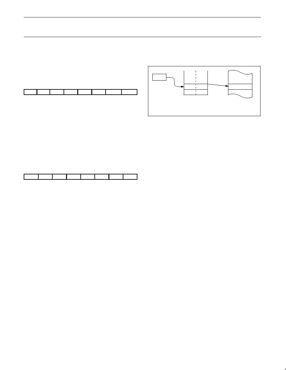
Philips Semiconductors
Product specification
8XC52/54/58/80C32
8XC51FA/FB/FC/80C51FA
8XC51RA+/RB+/RC+/RD+/80C51RA+
80C51 8-bit microcontroller family
8K≠64K/256≠1K OTP/ROM/ROMless, low voltage (2.7V≠5.5V),
low power, high speed (33MHz)
1999 Apr 01
24
Reduced EMI Mode
The AO bit (AUXR.0) in the AUXR register when set disables the
ALE output.
Reduced EMI Mode
AUXR (8EH)
7
6
5
4
3
2
1
0
≠
≠
≠
≠
≠
≠
EXTRAM
AO
AUXR.1
EXTRAM
(RX+ only)
AUXR.0
AO
Turns off ALE output.
Dual DPTR
The dual DPTR structure (see Figure 13) is a way by which the chip
will specify the address of an external data memory location. There
are two 16-bit DPTR registers that address the external memory,
and a single bit called DPS = AUXR1/bit0 that allows the program
code to switch between them.
∑
New Register Name: AUXR1#
∑
SFR Address: A2H
∑
Reset Value: xxxx00x0B
7
6
5
4
3
2
1
0
≠
≠
≠
LPEP
GF3
0
≠
DPS
Where:
DPS = AUXR1/bit0 = Switches between DPTR0 and DPTR1.
Select Reg
DPS
DPTR0
0
DPTR1
1
The DPS bit status should be saved by software when switching
between DPTR0 and DPTR1.
The GF3 bit is a general purpose user≠defined flag. Note that bit 2 is
not writable and is always read as a zero. This allows the DPS bit to
be quickly toggled simply by executing an INC DPTR instruction
without affecting the GF3 or LPEP bits.
DPS
DPTR1
DPTR0
DPH
(83H)
DPL
(82H)
EXTERNAL
DATA
MEMORY
SU00745A
BIT0
AUXR1
Figure 13.
DPTR Instructions
The instructions that refer to DPTR refer to the data pointer that is
currently selected using the AUXR1/bit 0 register. The six
instructions that use the DPTR are as follows:
INC DPTR
Increments the data pointer by 1
MOV DPTR, #data16
Loads the DPTR with a 16-bit constant
MOV A, @ A+DPTR
Move code byte relative to DPTR to ACC
MOVX A, @ DPTR
Move external RAM (16-bit address) to
ACC
MOVX @ DPTR , A
Move ACC to external RAM (16-bit
address)
JMP @ A + DPTR
Jump indirect relative to DPTR
The data pointer can be accessed on a byte-by-byte basis by
specifying the low or high byte in an instruction which accesses the
SFRs. See application note AN458 for more details.
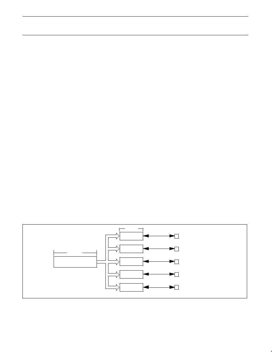
Philips Semiconductors
Product specification
8XC52/54/58/80C32
8XC51FA/FB/FC/80C51FA
8XC51RA+/RB+/RC+/RD+/80C51RA+
80C51 8-bit microcontroller family
8K≠64K/256≠1K OTP/ROM/ROMless, low voltage (2.7V≠5.5V),
low power, high speed (33MHz)
1999 Apr 01
25
(8XC51FX and 8XC51RX+ ONLY)
Programmable Counter Array (PCA)
(8XC51FX and 8XC51RX+ only)
The Programmable Counter Array available on the 8XC51FX and
8XC51RX+ is a special 16-bit Timer that has five 16-bit
capture/compare modules associated with it. Each of the modules
can be programmed to operate in one of four modes: rising and/or
falling edge capture, software timer, high-speed output, or pulse
width modulator. Each module has a pin associated with it in port 1.
Module 0 is connected to P1.3(CEX0), module 1 to P1.4(CEX1), etc.
The basic PCA configuration is shown in Figure 14.
The PCA timer is a common time base for all five modules and can
be programmed to run at: 1/12 the oscillator frequency, 1/4 the
oscillator frequency, the Timer 0 overflow, or the input on the ECI pin
(P1.2). The timer count source is determined from the CPS1 and
CPS0 bits in the CMOD SFR as follows (see Figure 17):
CPS1 CPS0 PCA Timer Count Source
0
0
1/12 oscillator frequency
0
1
1/4 oscillator frequency
1
0
Timer 0 overflow
1
1
External Input at ECI pin
In the CMOD SFR are three additional bits associated with the PCA.
They are CIDL which allows the PCA to stop during idle mode,
WDTE which enables or disables the watchdog function on
module 4, and ECF which when set causes an interrupt and the
PCA overflow flag CF (in the CCON SFR) to be set when the PCA
timer overflows. These functions are shown in Figure 15.
The watchdog timer function is implemented in module 4 (see
Figure 24).
The CCON SFR contains the run control bit for the PCA and the
flags for the PCA timer (CF) and each module (refer to Figure 18).
To run the PCA the CR bit (CCON.6) must be set by software. The
PCA is shut off by clearing this bit. The CF bit (CCON.7) is set when
the PCA counter overflows and an interrupt will be generated if the
ECF bit in the CMOD register is set, The CF bit can only be cleared
by software. Bits 0 through 4 of the CCON register are the flags for
the modules (bit 0 for module 0, bit 1 for module 1, etc.) and are set
by hardware when either a match or a capture occurs. These flags
also can only be cleared by software. The PCA interrupt system
shown in Figure 16.
Each module in the PCA has a special function register associated
with it. These registers are: CCAPM0 for module 0, CCAPM1 for
module 1, etc. (see Figure 19). The registers contain the bits that
control the mode that each module will operate in. The ECCF bit
(CCAPMn.0 where n=0, 1, 2, 3, or 4 depending on the module)
enables the CCF flag in the CCON SFR to generate an interrupt
when a match or compare occurs in the associated module. PWM
(CCAPMn.1) enables the pulse width modulation mode. The TOG
bit (CCAPMn.2) when set causes the CEX output associated with
the module to toggle when there is a match between the PCA
counter and the module's capture/compare register. The match bit
MAT (CCAPMn.3) when set will cause the CCFn bit in the CCON
register to be set when there is a match between the PCA counter
and the module's capture/compare register.
The next two bits CAPN (CCAPMn.4) and CAPP (CCAPMn.5)
determine the edge that a capture input will be active on. The CAPN
bit enables the negative edge, and the CAPP bit enables the
positive edge. If both bits are set both edges will be enabled and a
capture will occur for either transition. The last bit in the register
ECOM (CCAPMn.6) when set enables the comparator function.
Figure 20 shows the CCAPMn settings for the various PCA
functions.
There are two additional registers associated with each of the PCA
modules. They are CCAPnH and CCAPnL and these are the
registers that store the 16-bit count when a capture occurs or a
compare should occur. When a module is used in the PWM mode
these registers are used to control the duty cycle of the output.
MODULE FUNCTIONS:
16-BIT CAPTURE
16-BIT TIMER
16-BIT HIGH SPEED OUTPUT
8-BIT PWM
WATCHDOG TIMER (MODULE 4 ONLY)
MODULE 0
MODULE 1
MODULE 2
MODULE 3
MODULE 4
P1.3/CEX0
P1.4/CEX1
P1.5/CEX2
P1.6/CEX3
P1.7/CEX4
16 BITS
PCA TIMER/COUNTER
TIME BASE FOR PCA MODULES
16 BITS
SU00032
Figure 14. Programmable Counter Array (PCA)

Philips Semiconductors
Product specification
8XC52/54/58/80C32
8XC51FA/FB/FC/80C51FA
8XC51RA+/RB+/RC+/RD+/80C51RA+
80C51 8-bit microcontroller family
8K≠64K/256≠1K OTP/ROM/ROMless, low voltage (2.7V≠5.5V),
low power, high speed (33MHz)
1999 Apr 01
26
(8XC51FX and 8XC51RX+ ONLY)
CF
CR
CCF4
CCF3
CCF2
CCF1
CCF0
≠≠
CCON
(D8H)
CH
CL
OVERFLOW
INTERRUPT
16≠BIT UP COUNTER
IDLE
TO PCA
MODULES
CMOD
(D9H)
CIDL
WDTE
≠≠
≠≠
≠≠
CPS1
CPS0
ECF
OSC/12
OSC/4
TIMER 0
OVERFLOW
EXTERNAL INPUT
(P1.2/ECI)
DECODE
00
01
10
11
SU00033
Figure 15. PCA Timer/Counter
MODULE 0
MODULE 1
MODULE 2
MODULE 3
MODULE 4
PCA TIMER/COUNTER
CF
CR
CCF4
CCF3
CCF2
CCF1
CCF0
≠≠
CMOD.0 ECF
CCAPMn.0 ECCFn
TO
INTERRUPT
PRIORITY
DECODER
CCON
(D8H)
IE.6
EC
IE.7
EA
SU00034
Figure 16. PCA Interrupt System

Philips Semiconductors
Product specification
8XC52/54/58/80C32
8XC51FA/FB/FC/80C51FA
8XC51RA+/RB+/RC+/RD+/80C51RA+
80C51 8-bit microcontroller family
8K≠64K/256≠1K OTP/ROM/ROMless, low voltage (2.7V≠5.5V),
low power, high speed (33MHz)
1999 Apr 01
27
(8XC51FX and 8XC51RX+ ONLY)
CMOD Address = OD9H
Reset Value = 00XX X000B
CIDL
WDTE
≠
≠
≠
CPS1
CPS0
ECF
Bit:
Symbol
Function
CIDL
Counter Idle control: CIDL = 0 programs the PCA Counter to continue functioning during idle Mode. CIDL = 1 programs
it to be gated off during idle.
WDTE
Watchdog Timer Enable: WDTE = 0 disables Watchdog Timer function on PCA Module 4. WDTE = 1 enables it.
≠
Not implemented, reserved for future use.*
CPS1
PCA Count Pulse Select bit 1.
CPS0
PCA Count Pulse Select bit 0.
CPS1
CPS0
Selected PCA Input**
0
0
0
Internal clock, f
OSC
˜
12
0
1
1
Internal clock, f
OSC
˜
4
1
0
2
Timer 0 overflow
1
1
3
External clock at ECI/P1.2 pin (max. rate = f
OSC
˜
8)
ECF
PCA Enable Counter Overflow interrupt: ECF = 1 enables CF bit in CCON to generate an interrupt. ECF = 0 disables
that function of CF.
NOTE:
*
User software should not write 1s to reserved bits. These bits may be used in future 8051 family products to invoke new features. In that case, the reset or inactive value of the
new bit will be 0, and its active value will be 1. The value read from a reserved bit is indeterminate.
** f
OSC
= oscillator frequency
SU00035
7
6
5
4
3
2
1
0
Figure 17. CMOD: PCA Counter Mode Register
CCON Address = OD8H
Reset Value = 00X0 0000B
CF
CR
≠
CCF4
CCF3
CCF2
CCF1
CCF0
Bit Addressable
Bit:
Symbol
Function
CF
PCA Counter Overflow flag. Set by hardware when the counter rolls over. CF flags an interrupt if bit ECF in CMOD is
set. CF may be set by either hardware or software but can only be cleared by software.
CR
PCA Counter Run control bit. Set by software to turn the PCA counter on. Must be cleared by software to turn the PCA
counter off.
≠
Not implemented, reserved for future use*.
CCF4
PCA Module 4 interrupt flag. Set by hardware when a match or capture occurs. Must be cleared by software.
CCF3
PCA Module 3 interrupt flag. Set by hardware when a match or capture occurs. Must be cleared by software.
CCF2
PCA Module 2 interrupt flag. Set by hardware when a match or capture occurs. Must be cleared by software.
CCF1
PCA Module 1 interrupt flag. Set by hardware when a match or capture occurs. Must be cleared by software.
CCF0
PCA Module 0 interrupt flag. Set by hardware when a match or capture occurs. Must be cleared by software.
NOTE:
*
User software should not write 1s to reserved bits. These bits may be used in future 8051 family products to invoke new features. In that case, the reset or inactive value of the
new bit will be 0, and its active value will be 1. The value read from a reserved bit is indeterminate.
SU00036
7
6
5
4
3
2
1
0
Figure 18. CCON: PCA Counter Control Register
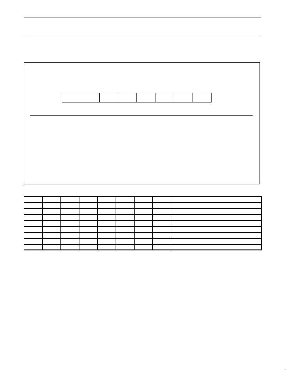
Philips Semiconductors
Product specification
8XC52/54/58/80C32
8XC51FA/FB/FC/80C51FA
8XC51RA+/RB+/RC+/RD+/80C51RA+
80C51 8-bit microcontroller family
8K≠64K/256≠1K OTP/ROM/ROMless, low voltage (2.7V≠5.5V),
low power, high speed (33MHz)
1999 Apr 01
28
(8XC51FX and 8XC51RX+ ONLY)
CCAPMn Address
CCAPM0
0DAH
CCAPM1
0DBH
CCAPM2
0DCH
CCAPM3
0DDH
CCAPM4
0DEH
Reset Value = X000 0000B
≠
ECOMn
CAPPn
CAPNn
MATn
TOGn
PWMn
ECCFn
Not Bit Addressable
Bit:
Symbol
Function
≠
Not implemented, reserved for future use*.
ECOMn
Enable Comparator. ECOMn = 1 enables the comparator function.
CAPPn
Capture Positive, CAPPn = 1 enables positive edge capture.
CAPNn
Capture Negative, CAPNn = 1 enables negative edge capture.
MATn
Match. When MATn = 1, a match of the PCA counter with this module's compare/capture register causes the CCFn bit
in CCON to be set, flagging an interrupt.
TOGn
Toggle. When TOGn = 1, a match of the PCA counter with this module's compare/capture register causes the CEXn
pin to toggle.
PWMn
Pulse Width Modulation Mode. PWMn = 1 enables the CEXn pin to be used as a pulse width modulated output.
ECCFn
Enable CCF interrupt. Enables compare/capture flag CCFn in the CCON register to generate an interrupt.
NOTE:
*User software should not write 1s to reserved bits. These bits may be used in future 8051 family products to invoke new features. In that case, the reset or inactive value of the new
bit will be 0, and its active value will be 1. The value read from a reserved bit is indeterminate.
SU00037
7
6
5
4
3
2
1
0
Figure 19. CCAPMn: PCA Modules Compare/Capture Registers
≠
ECOMn
CAPPn
CAPNn
MATn
TOGn
PWMn
ECCFn
MODULE FUNCTION
X
0
0
0
0
0
0
0
No operation
X
X
1
0
0
0
0
X
16-bit capture by a positive-edge trigger on CEXn
X
X
0
1
0
0
0
X
16-bit capture by a negative trigger on CEXn
X
X
1
1
0
0
0
X
16-bit capture by a transition on CEXn
X
1
0
0
1
0
0
X
16-bit Software Timer
X
1
0
0
1
1
0
X
16-bit High Speed Output
X
1
0
0
0
0
1
0
8-bit PWM
X
1
0
0
1
X
0
X
Watchdog Timer
Figure 20. PCA Module Modes (CCAPMn Register)
PCA Capture Mode
To use one of the PCA modules in the capture mode either one or
both of the CCAPM bits CAPN and CAPP for that module must be
set. The external CEX input for the module (on port 1) is sampled for
a transition. When a valid transition occurs the PCA hardware loads
the value of the PCA counter registers (CH and CL) into the
module's capture registers (CCAPnL and CCAPnH). If the CCFn bit
for the module in the CCON SFR and the ECCFn bit in the CCAPMn
SFR are set then an interrupt will be generated. Refer to Figure 21.
16-bit Software Timer Mode
The PCA modules can be used as software timers by setting both
the ECOM and MAT bits in the modules CCAPMn register. The PCA
timer will be compared to the module's capture registers and when a
match occurs an interrupt will occur if the CCFn (CCON SFR) and
the ECCFn (CCAPMn SFR) bits for the module are both set (see
Figure 22).
High Speed Output Mode
In this mode the CEX output (on port 1) associated with the PCA
module will toggle each time a match occurs between the PCA
counter and the module's capture registers. To activate this mode
the TOG, MAT, and ECOM bits in the module's CCAPMn SFR must
be set (see Figure 23).
Pulse Width Modulator Mode
All of the PCA modules can be used as PWM outputs. Figure 24
shows the PWM function. The frequency of the output depends on
the source for the PCA timer. All of the modules will have the same
frequency of output because they all share the PCA timer. The duty
cycle of each module is independently variable using the module's
capture register CCAPLn. When the value of the PCA CL SFR is
less than the value in the module's CCAPLn SFR the output will be
low, when it is equal to or greater than the output will be high. When
CL overflows from FF to 00, CCAPLn is reloaded with the value in
CCAPHn. the allows updating the PWM without glitches. The PWM
and ECOM bits in the module's CCAPMn register must be set to
enable the PWM mode.

Philips Semiconductors
Product specification
8XC52/54/58/80C32
8XC51FA/FB/FC/80C51FA
8XC51RA+/RB+/RC+/RD+/80C51RA+
80C51 8-bit microcontroller family
8K≠64K/256≠1K OTP/ROM/ROMless, low voltage (2.7V≠5.5V),
low power, high speed (33MHz)
1999 Apr 01
29
(8XC51FX and 8XC51RX+ ONLY)
CF
CR
CCF4
CCF3
CCF2
CCF1
CCF0
≠≠
CCON
(D8H)
≠≠
ECOMn
CAPPn
CAPNn
MATn
TOGn
PWMn
ECCFn
CCAPMn, n= 0 to 4
(DAH ≠ DEH)
CH
CL
CCAPnH
CCAPnL
CEXn
CAPTURE
PCA INTERRUPT
PCA TIMER/COUNTER
0
0
0
0
(TO CCFn)
SU00749
Figure 21. PCA Capture Mode
MATCH
CF
CR
CCF4
CCF3
CCF2
CCF1
CCF0
≠≠
CCON
(D8H)
≠≠
ECOMn
CAPPn
CAPNn
MATn
TOGn
PWMn
ECCFn
CCAPMn, n= 0 to 4
(DAH ≠ DEH)
CH
CL
CCAPnH
CCAPnL
PCA INTERRUPT
PCA TIMER/COUNTER
0
0
0
0
16≠BIT COMPARATOR
(TO CCFn)
ENABLE
WRITE TO
CCAPnH
RESET
WRITE TO
CCAPnL
0
1
SU00750
Figure 22. PCA Compare Mode
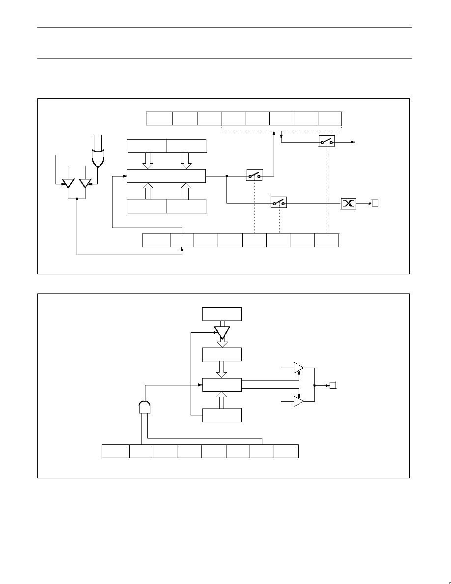
Philips Semiconductors
Product specification
8XC52/54/58/80C32
8XC51FA/FB/FC/80C51FA
8XC51RA+/RB+/RC+/RD+/80C51RA+
80C51 8-bit microcontroller family
8K≠64K/256≠1K OTP/ROM/ROMless, low voltage (2.7V≠5.5V),
low power, high speed (33MHz)
1999 Apr 01
30
(8XC51FX and 8XC51RX+ ONLY)
CF
CR
CCF4
CCF3
CCF2
CCF1
CCF0
≠≠
CCON
(D8H)
≠≠
ECOMn
CAPPn
CAPNn
MATn
TOGn
PWMn
ECCFn
CCAPMn, n: 0..4
(DAH ≠ DEH)
CH
CL
CCAPnH
CCAPnL
PCA INTERRUPT
PCA TIMER/COUNTER
1
0
0
0
16≠BIT COMPARATOR
(TO CCFn)
WRITE TO
CCAPnH
RESET
WRITE TO
CCAPnL
0
1
ENABLE
CEXn
TOGGLE
MATCH
SU00751
Figure 23. PCA High Speed Output Mode
CL < CCAPnL
≠≠
ECOMn
CAPPn
CAPNn
MATn
TOGn
PWMn
ECCFn
CCAPMn, n: 0..4
(DAH ≠ DEH)
PCA TIMER/COUNTER
0
0
0
0
CL
CCAPnL
CEXn
8≠BIT
COMPARATOR
OVERFLOW
CCAPnH
ENABLE
0
1
CL >= CCAPnL
0
SU00752
Figure 24. PCA PWM Mode

Philips Semiconductors
Product specification
8XC52/54/58/80C32
8XC51FA/FB/FC/80C51FA
8XC51RA+/RB+/RC+/RD+/80C51RA+
80C51 8-bit microcontroller family
8K≠64K/256≠1K OTP/ROM/ROMless, low voltage (2.7V≠5.5V),
low power, high speed (33MHz)
1999 Apr 01
31
(8XC51FX and 8XC51RX+ ONLY)
≠≠
ECOMn
CAPPn
CAPNn
MATn
TOGn
PWMn
ECCFn
CCAPM4
(DEH)
CH
CL
CCAP4H
CCAP4L
RESET
PCA TIMER/COUNTER
X
0
0
0
16≠BIT COMPARATOR
MATCH
ENABLE
WRITE TO
CCAP4H
RESET
WRITE TO
CCAP4L
0
1
1
CMOD
(D9H)
CIDL
WDTE
≠≠
≠≠
≠≠
CPS1
CPS0
ECF
X
SU00832
MODULE 4
Figure 25. PCA Watchdog Timer m(Module 4 only)
PCA Watchdog Timer
An on-board watchdog timer is available with the PCA to improve
the reliability of the system without increasing chip count. Watchdog
timers are useful for systems that are susceptible to noise, power
glitches, or electrostatic discharge. Module 4 is the only PCA
module that can be programmed as a watchdog. However, this
module can still be used for other modes if the watchdog is not
needed.
Figure 25 shows a diagram of how the watchdog works. The user
pre-loads a 16-bit value in the compare registers. Just like the other
compare modes, this 16-bit value is compared to the PCA timer
value. If a match is allowed to occur, an internal reset will be
generated. This will not cause the RST pin to be driven high.
In order to hold off the reset, the user has three options:
1. periodically change the compare value so it will never match the
PCA timer,
2. periodically change the PCA timer value so it will never match
the compare values, or
3. disable the watchdog by clearing the WDTE bit before a match
occurs and then re-enable it.
The first two options are more reliable because the watchdog timer
is never disabled as in option #3. If the program counter ever goes
astray, a match will eventually occur and cause an internal reset.
The second option is also not recommended if other PCA modules
are being used. Remember, the PCA timer is the time base for all
modules; changing the time base for other modules would not be a
good idea. Thus, in most applications the first solution is the best
option.
Figure 26 shows the code for initializing the watchdog timer.
Module 4 can be configured in either compare mode, and the WDTE
bit in CMOD must also be set. The user's software then must
periodically change (CCAP4H,CCAP4L) to keep a match from
occurring with the PCA timer (CH,CL). This code is given in the
WATCHDOG routine in Figure 26.
This routine should not be part of an interrupt service routine,
because if the program counter goes astray and gets stuck in an
infinite loop, interrupts will still be serviced and the watchdog will
keep getting reset. Thus, the purpose of the watchdog would be
defeated. Instead, call this subroutine from the main program within
2
16
count of the PCA timer.

Philips Semiconductors
Product specification
8XC52/54/58/80C32
8XC51FA/FB/FC/80C51FA
8XC51RA+/RB+/RC+/RD+/80C51RA+
80C51 8-bit microcontroller family
8K≠64K/256≠1K OTP/ROM/ROMless, low voltage (2.7V≠5.5V),
low power, high speed (33MHz)
1999 Apr 01
32
(8XC51FX and 8XC51RX+ ONLY)
INIT_WATCHDOG:
MOV CCAPM4, #4CH ; Module 4 in compare mode
MOV CCAP4L, #0FFH ; Write to low byte first
MOV CCAP4H, #0FFH ; Before PCA timer counts up to
; FFFF Hex, these compare values
; must be changed
ORL CMOD, #40H ; Set the WDTE bit to enable the
; watchdog timer without changing
; the other bits in CMOD
;
;********************************************************************
;
; Main program goes here, but CALL WATCHDOG periodically.
;
;********************************************************************
;
WATCHDOG:
CLR EA ; Hold off interrupts
MOV CCAP4L, #00 ; Next compare value is within
MOV CCAP4H, CH ; 255 counts of the current PCA
SETB EA ; timer value
RET
Figure 26. PCA Watchdog Timer Initialization Code

Philips Semiconductors
Product specification
8XC52/54/58/80C32
8XC51FA/FB/FC/80C51FA
8XC51RA+/RB+/RC+/RD+/80C51RA+
80C51 8-bit microcontroller family
8K≠64K/256≠1K OTP/ROM/ROMless, low voltage (2.7V≠5.5V),
low power, high speed (33MHz)
1999 Apr 01
33
(8XC51RX+ ONLY)
Expanded Data RAM Addressing
(8XC51RX+ ONLY)
The 8XC51RX+ have internal data memory that is mapped into four
separate segments: the lower 128 bytes of RAM, upper 128 bytes of
RAM, 128 bytes Special Function Register (SFR), and 256 bytes
(768 for RD+) expanded RAM (EXTRAM).
The four segments are:
1. The Lower 128 bytes of RAM (addresses 00H to 7FH) are
directly and indirectly addressable.
2. The Upper 128 bytes of RAM (addresses 80H to FFH) are
indirectly addressable only.
3. The Special Function Registers, SFRs, (addresses 80H to FFH)
are directly addressable only.
4. The 256-bytes (768 for RD+) expanded RAM ((EXTRAM
(256-bytes) 00H≠FFH)) and ((EXTRAM (768-bytes for RD+)
00H ≠ 2FFH)) are indirectly accessed by move external instruction,
MOVX, and with the EXTRAM bit cleared, see Figure 27.
The Lower 128 bytes can be accessed by either direct or indirect
addressing. The Upper 128 bytes can be accessed by indirect
addressing only. The Upper 128 bytes occupy the same address
space as the SFR. That means they have the same address, but are
physically separate from SFR space.
When an instruction accesses an internal location above address
7FH, the CPU knows whether the access is to the upper 128 bytes
of data RAM or to SFR space by the addressing mode used in the
instruction. Instructions that use direct addressing access SFR
space. For example:
MOV 0A0H,#data
accesses the SFR at location 0A0H (which is P2). Instructions that
use indirect addressing access the Upper 128 bytes of data RAM.
For example:
MOV @R0,#data
where R0 contains 0A0H, accesses the data byte at address 0A0H,
rather than P2 (whose address is 0A0H).
The EXTRAM can be accessed by indirect addressing, with
EXTRAM bit cleared and MOVX instructions. This part of memory is
physically located on-chip, logically occupies the first 256-bytes (768
for RD+) of external data memory.
With EXTRAM = 0, the EXTRAM is indirectly addressed, using the
MOVX instruction in combination with any of the registers R0, R1 of
the selected bank or DPTR. An access to EXTRAM will not affect
ports P0, P3.6 (WR#) and P3.7 (RD#). P2 SFR is output during
external addressing. For example, with EXTRAM = 0,
MOVX @R0,#data
where R0 contains 0A0H, access the EXTRAM at address 0A0H
rather than external memory. An access to external data memory
locations higher than FFH (2FF for RD+) (i.e., 0100H to FFFFH) will
be performed with the MOVX DPTR instructions in the same way as
in the standard 80C51, so with P0 and P2 as data/address bus, and
P3.6 and P3.7 as write and read timing signals. Refer to Figure 28.
With EXTRAM = 1, MOVX @Ri and MOVX @DPTR will be similar
to the standard 80C51. MOVX @ Ri will provide an 8-bit address
multiplexed with data on Port 0 and any output port pins can be
used to output higher order address bits. This is to provide the
external paging capability. MOVX @DPTR will generate a 16-bit
address. Port 2 outputs the high-order eight address bits (the
contents of DPH) while Port 0 multiplexes the low-order eight
address bits (DPL) with data. MOVX @Ri and MOVX @DPTR will
generate either read or write signals on P3.6 (#WR) and P3.7 (#RD).
The stack pointer (SP) may be located anywhere in the 256 bytes
RAM (lower and upper RAM) internal data memory. The stack may
not be located in the EXTRAM.
AUXR
Reset Value = xxxx xx00B
--
--
--
--
--
--
EXTRAM
AO
Not Bit Addressable
Bit:
Symbol
Function
AO
Disable/Enable ALE
AO
Operating Mode
0
ALE is emitted at a constant rate of 1/6 the oscillator frequency.
1
ALE is active only during a MOVX or MOVC instruction.
EXTRAM
Internal/External RAM access using MOVX @Ri/@DPTR
EXTRAM
Operating Mode
0
Internal ERAM (00H≠FFH) (00H≠2FFH for RD+) access using MOVX @Ri/@DPTR
1
External data memory access.
--
Not implemented, reserved for future use*.
NOTE:
*User software should not write 1s to reserved bits. These bits may be used in future 8051 family products to invoke new features. In that case, the reset or inactive value of the new
bit will be 0, and its active value will be 1. The value read from a reserved bit is indeterminate.
SU01003
7
6
5
4
3
2
1
0
Address = 8EH
Figure 27. AUXR: Auxiliary Register (RX+ only)
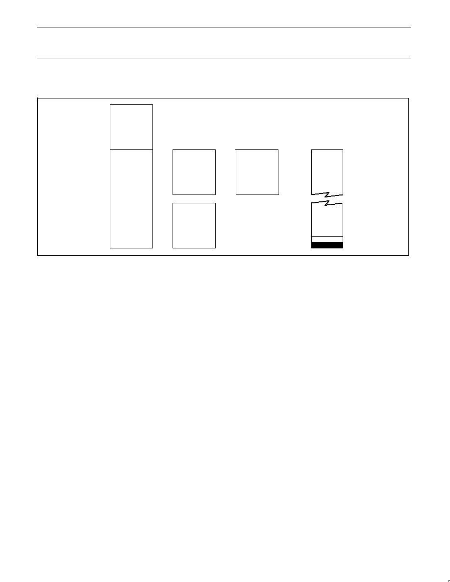
Philips Semiconductors
Product specification
8XC52/54/58/80C32
8XC51FA/FB/FC/80C51FA
8XC51RA+/RB+/RC+/RD+/80C51RA+
80C51 8-bit microcontroller family
8K≠64K/256≠1K OTP/ROM/ROMless, low voltage (2.7V≠5.5V),
low power, high speed (33MHz)
1999 Apr 01
34
(8XC51RX+ ONLY)
ERAM
256 BYTES
UPPER
128 BYTES
INTERNAL RAM
LOWER
128 BYTES
INTERNAL RAM
SPECIAL
FUNCTION
REGISTER
……………
……………
……………
……………
……………
2FF
(RD TO RD+)
FF
00
FF
00
FF
00
80
80
EXTERNAL
DATA
MEMORY
FFFF
0000
0100
300 (RD+ only)
SU00834
Figure 28. Internal and External Data Memory Address Space with EXTRAM = 0
HARDWARE WATCHDOG TIMER (ONE-TIME
ENABLED WITH RESET-OUT FOR 89C51RC+/RD+)
The WDT is intended as a recovery method in situations where the
CPU may be subjected to software upset. The WDT consists of a
14-bit counter and the WatchDog Timer reset (WDTRST) SFR. The
WDT is disabled at reset. To enable the WDT, user must write 01EH
and 0E1H in sequence to the WDTRST, SFR location 0A6H. When
WDT is enabled, it will increment every machine cycle while the
oscillator is running and there is no way to disable the WDT except
through reset (either hardware reset or WDT overflow reset). When
WDT overflows, it will drive an output reset HIGH pulse at the
RST-pin.
Using the WDT
To enable the WDT, user must write 01EH and 0E1H in sequence to
the WDTRST, SFR location 0A6H. When WDT is enabled, the user
needs to service it by writing to 01EH and 0E1H to WDTRST to
avoid WDT overflow. The 14-bit counter overflows when it reaches
16383 (3FFFH) and this will reset the device. When using the WDT,
a 1Kohm resistor must be inserted between RST of the device and
the Power On Reset circuitry. When WDT is enabled, it will
increment every machine cycle while the oscillator is running. This
means the user must reset the WDT at least every 16383 machine
cycles. To reset the WDT, the user must write 01EH and 0E1H to
WDTRST. WDTRST is a write only register. The WDT counter
cannot be read or written. When WDT overflows, it will generate an
output RESET pulse at the reset pin. The RESET pulse duration is
98
◊
T
OSC
, where T
OSC
= 1/f
OSC
. To make the best use of the WDT,
it should be serviced in those sections of code that will periodically
be executed within the time required to prevent a WDT reset.
In applications using the Hardware Watchdog Timer of the
P8xC51RD+, a series resistor (1K
W
"
20%) needs to be included
between the reset pin and any external components. Without this
resistor the watchdog timer will not function.
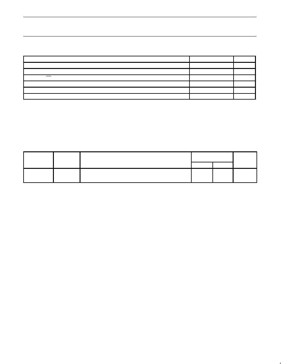
Philips Semiconductors
Product specification
8XC52/54/58/80C32
8XC51FA/FB/FC/80C51FA
8XC51RA+/RB+/RC+/RD+/80C51RA+
80C51 8-bit microcontroller family
8K≠64K/256≠1K OTP/ROM/ROMless, low voltage (2.7V≠5.5V),
low power, high speed (33MHz)
1999 Apr 01
35
ABSOLUTE MAXIMUM RATINGS
1, 2, 3
PARAMETER
RATING
UNIT
Operating temperature under bias
0 to +70 or ≠40 to +85
∞
C
Storage temperature range
≠65 to +150
∞
C
Voltage on EA/V
PP
pin to V
SS
0 to +13.0
V
Voltage on any other pin to V
SS
≠0.5 to +6.5
V
Maximum I
OL
per I/O pin
15
mA
Power dissipation (based on package heat transfer limitations, not device power consumption)
1.5
W
NOTES:
1. Stresses above those listed under Absolute Maximum Ratings may cause permanent damage to the device. This is a stress rating only and
functional operation of the device at these or any conditions other than those described in the AC and DC Electrical Characteristics section
of this specification is not implied.
2. This product includes circuitry specifically designed for the protection of its internal devices from the damaging effects of excessive static
charge. Nonetheless, it is suggested that conventional precautions be taken to avoid applying greater than the rated maximum.
3. Parameters are valid over operating temperature range unless otherwise specified. All voltages are with respect to V
SS
unless otherwise
noted.
AC ELECTRICAL CHARACTERISTICS
T
amb
= 0
∞
C to +70
∞
C or ≠40
∞
C to +85
∞
C
CLOCK FREQUENCY
RANGE ≠f
SYMBOL
FIGURE
PARAMETER
MIN
MAX
UNIT
1/t
CLCL
33
Oscillator frequency
Speed versions : 4:5:S (16MHz)
I:J:U (33MHz)
0
0
16
33
MHz
MHz

Philips Semiconductors
Product specification
8XC52/54/58/80C32
8XC51FA/FB/FC/80C51FA
8XC51RA+/RB+/RC+/RD+/80C51RA+
80C51 8-bit microcontroller family
8K≠64K/256≠1K OTP/ROM/ROMless, low voltage (2.7V≠5.5V),
low power, high speed (33MHz)
1999 Apr 01
36
DC ELECTRICAL CHARACTERISTICS
T
amb
= 0
∞
C to +70
∞
C or ≠40
∞
C to +85
∞
C, V
CC
= 2.7V to 5.5V, V
SS
= 0V (16MHz devices)
SYMBOL
PARAMETER
TEST
LIMITS
UNIT
SYMBOL
PARAMETER
CONDITIONS
MIN
TYP
1
MAX
UNIT
V
Input low voltage
4.0V < V
CC
< 5.5V
≠0.5
0.2V
CC
≠0.1
V
V
IL
Input low voltage
2.7V<V
CC
< 4.0V
≠0.5
0.7
V
V
IH
Input high voltage (ports 0, 1, 2, 3, EA)
0.2V
CC
+0.9
V
CC
+0.5
V
V
IH1
Input high voltage, XTAL1, RST
0.7V
CC
V
CC
+0.5
V
V
OL
Output low voltage, ports 1, 2
8
V
CC
= 2.7V
I
OL
= 1.6mA
2
0.4
V
V
OL1
Output low voltage, port 0, ALE, PSEN
8, 7
V
CC
= 2.7V
I
OL
= 3.2mA
2
0.4
V
V
O
Output high voltage ports 1 2 3
3
V
CC
= 2.7V
I
OH
= ≠20
µ
A
V
CC
≠ 0.7
V
V
OH
Output high voltage, ports 1, 2, 3
3
V
CC
= 4.5V
I
OH
= ≠30
µ
A
V
CC
≠ 0.7
V
V
OH1
Output high voltage (port 0 in external bus mode),
ALE
9
, PSEN
3
V
CC
= 2.7V
I
OH
= ≠3.2mA
V
CC
≠ 0.7
V
I
IL
Logical 0 input current, ports 1, 2, 3
V
IN
= 0.4V
≠1
≠50
µ
A
I
TL
Logical 1-to-0 transition current, ports 1, 2, 3
6
V
IN
= 2.0V
See note 4
≠650
µ
A
I
LI
Input leakage current, port 0
0.45 < V
IN
< V
CC
≠ 0.3
±
10
µ
A
I
CC
Power supply current (see Figure 36):
See note 5
Active mode @ 16MHz (all except 8XC51RD+)
87C51RD+
15
16
mA
mA
Idle mode @ 16MHz
4
mA
Power-down mode or clock stopped (see Figure 40
f
diti
)
T
amb
= 0
∞
C to 70
∞
C
3
50
µ
A
for conditions)
T
amb
= ≠40
∞
C to +85
∞
C
75
µ
A
R
RST
Internal reset pull-down resistor
40
225
k
C
IO
Pin capacitance
10
(except EA)
15
pF
NOTES:
1. Typical ratings are not guaranteed. The values listed are at room temperature, 5V.
2. Capacitive loading on ports 0 and 2 may cause spurious noise to be superimposed on the V
OL
s of ALE and ports 1 and 3. The noise is due
to external bus capacitance discharging into the port 0 and port 2 pins when these pins make 1-to-0 transitions during bus operations. In the
worst cases (capacitive loading > 100pF), the noise pulse on the ALE pin may exceed 0.8V. In such cases, it may be desirable to qualify
ALE with a Schmitt Trigger, or use an address latch with a Schmitt Trigger STROBE input. I
OL
can exceed these conditions provided that no
single output sinks more than 5mA and no more than two outputs exceed the test conditions.
3. Capacitive loading on ports 0 and 2 may cause the V
OH
on ALE and PSEN to momentarily fall below the V
CC
≠0.7 specification when the
address bits are stabilizing.
4. Pins of ports 1, 2 and 3 source a transition current when they are being externally driven from 1 to 0. The transition current reaches its
maximum value when V
IN
is approximately 2V.
5. See Figures 37 through 40 for I
CC
test conditions, and Figure 36 for I
CC
vs Freq.
Active mode:
I
CC
= (0.9
◊
FREQ. + 1.1)mA for all devices except 8XC51RD+; 8XC51RD+ I
CC
= (0.9 x Freq +2.1) mA
Idle mode:
I
CC
= (0.18
◊
FREQ. +1.01)mA
6. This value applies to T
amb
= 0
∞
C to +70
∞
C. For T
amb
= ≠40
∞
C to +85
∞
C, I
TL
= ≠750
µ
A.
7. Load capacitance for port 0, ALE, and PSEN = 100pF, load capacitance for all other outputs = 80pF.
8. Under steady state (non-transient) conditions, I
OL
must be externally limited as follows:
Maximum I
OL
per port pin:
15mA (*NOTE: This is 85
∞
C specification.)
Maximum I
OL
per 8-bit port:
26mA
Maximum total I
OL
for all outputs:
71mA
If I
OL
exceeds the test condition, V
OL
may exceed the related specification. Pins are not guaranteed to sink current greater than the listed
test conditions.
9. ALE is tested to V
OH1
, except when ALE is off then V
OH
is the voltage specification.
10. Pin capacitance is characterized but not tested. Pin capacitance is less than 25pF. Pin capacitance of ceramic package is less than 15pF
(except EA is 25pF).
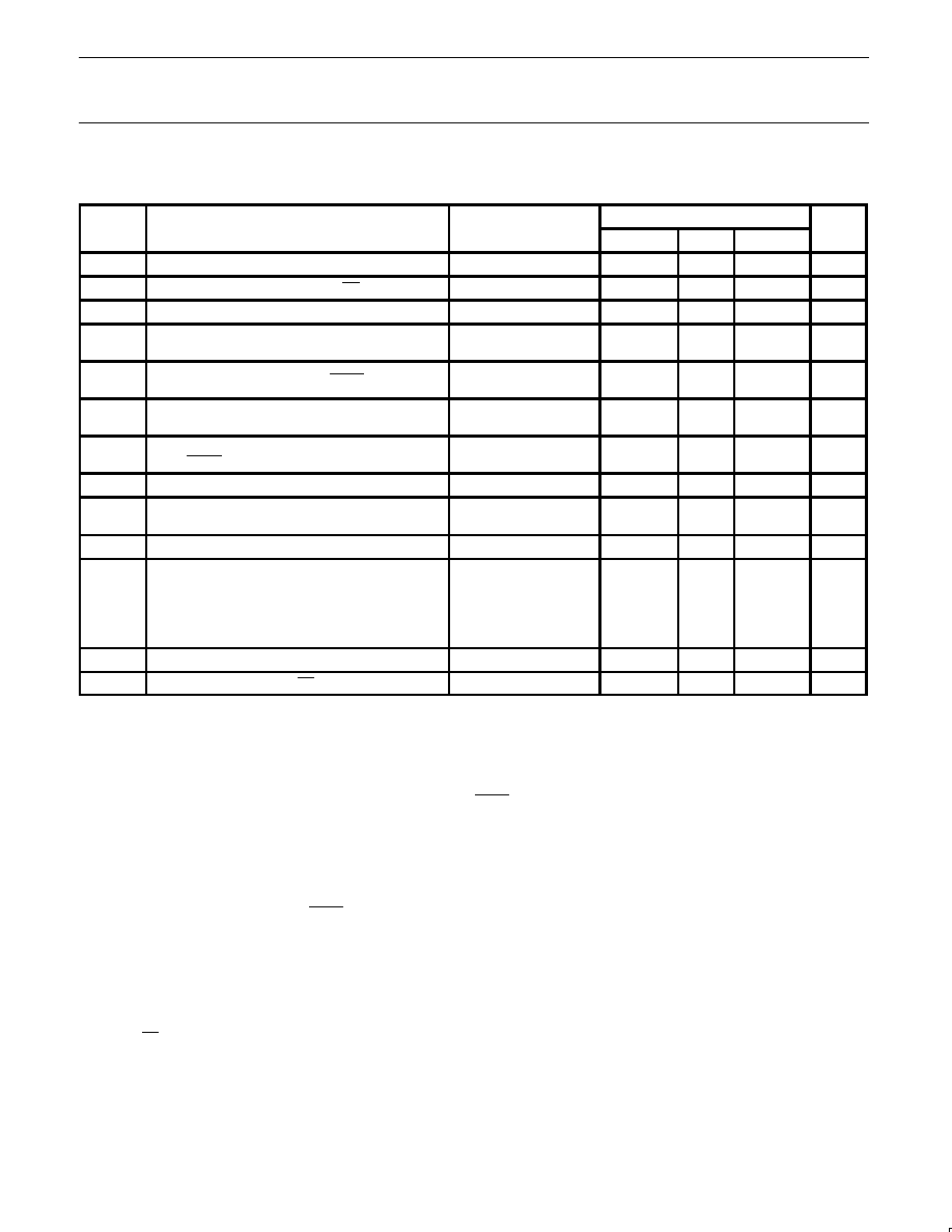
Philips Semiconductors
Product specification
8XC52/54/58/80C32
8XC51FA/FB/FC/80C51FA
8XC51RA+/RB+/RC+/RD+/80C51RA+
80C51 8-bit microcontroller family
8K≠64K/256≠1K OTP/ROM/ROMless, low voltage (2.7V≠5.5V),
low power, high speed (33MHz)
1999 Apr 01
37
DC ELECTRICAL CHARACTERISTICS
T
amb
= 0
∞
C to +70
∞
C or ≠40
∞
C to +85
∞
C, 33MHz devices; 5V
±
10%; V
SS
= 0V
SYMBOL
PARAMETER
TEST
LIMITS
UNIT
SYMBOL
PARAMETER
CONDITIONS
MIN
TYP
1
MAX
UNIT
V
IL
Input low voltage
4.5V < V
CC
< 5.5V
≠0.5
0.2V
CC
≠0.1
V
V
IH
Input high voltage (ports 0, 1, 2, 3, EA)
0.2V
CC
+0.9
V
CC
+0.5
V
V
IH1
Input high voltage, XTAL1, RST
0.7V
CC
V
CC
+0.5
V
V
OL
Output low voltage, ports 1, 2, 3
8
V
CC
= 4.5V
I
OL
= 1.6mA
2
0.4
V
V
OL1
Output low voltage, port 0, ALE, PSEN
7, 8
V
CC
= 4.5V
I
OL
= 3.2mA
2
0.4
V
V
OH
Output high voltage, ports 1, 2, 3
3
V
CC
= 4.5V
I
OH
= ≠30
µ
A
V
CC
≠ 0.7
V
V
OH1
Output high voltage (port 0 in external bus mode),
ALE
9
, PSEN
3
V
CC
= 4.5V
I
OH
= ≠3.2mA
V
CC
≠ 0.7
V
I
IL
Logical 0 input current, ports 1, 2, 3
V
IN
= 0.4V
≠1
≠50
µ
A
I
TL
Logical 1-to-0 transition current, ports 1, 2, 3
6
V
IN
= 2.0V
See note 4
≠650
µ
A
I
LI
Input leakage current, port 0
0.45 < V
IN
< V
CC
≠ 0.3
±
10
µ
A
I
CC
Power supply current (see Figure 36):
See note 5
Active mode (see Note 5)
Idle mode (see Note 5)
Power-down mode or clock stopped
(
Fi
40 f
diti
)
T
amb
= 0
∞
C to 70
∞
C
3
50
µ
A
(see Figure 40 for conditions)
T
amb
= ≠40
∞
C to +85
∞
C
75
µ
A
R
RST
Internal reset pull-down resistor
40
225
k
C
IO
Pin capacitance
10
(except EA)
15
pF
NOTES:
1. Typical ratings are not guaranteed. The values listed are at room temperature, 5V.
2. Capacitive loading on ports 0 and 2 may cause spurious noise to be superimposed on the V
OL
s of ALE and ports 1 and 3. The noise is due
to external bus capacitance discharging into the port 0 and port 2 pins when these pins make 1-to-0 transitions during bus operations. In the
worst cases (capacitive loading > 100pF), the noise pulse on the ALE pin may exceed 0.8V. In such cases, it may be desirable to qualify
ALE with a Schmitt Trigger, or use an address latch with a Schmitt Trigger STROBE input. I
OL
can exceed these conditions provided that no
single output sinks more than 5mA and no more than two outputs exceed the test conditions.
3. Capacitive loading on ports 0 and 2 may cause the V
OH
on ALE and PSEN to momentarily fall below the V
CC
≠0.7 specification when the
address bits are stabilizing.
4. Pins of ports 1, 2 and 3 source a transition current when they are being externally driven from 1 to 0. The transition current reaches its
maximum value when V
IN
is approximately 2V.
5. See Figures 37 through 40 for I
CC
test conditions and Figure 36 for I
CC
vs Freq.
Active mode:
I
CC(MAX)
= (0.9
◊
FREQ. + 1.1)mA. for all devices except 8XC51RD+; 8XC51RD+ I
CC
= (0.9 x Freq +2.1) mA
Idle mode:
I
CC(MAX)
= (0.18
◊
FREQ. +1.0)mA
6. This value applies to T
amb
= 0
∞
C to +70
∞
C. For T
amb
= ≠40
∞
C to +85
∞
C, I
TL
= ≠750
µ
A.
7. Load capacitance for port 0, ALE, and PSEN = 100pF, load capacitance for all other outputs = 80pF.
8. Under steady state (non-transient) conditions, I
OL
must be externally limited as follows:
Maximum I
OL
per port pin:
15mA (*NOTE: This is 85
∞
C specification.)
Maximum I
OL
per 8-bit port:
26mA
Maximum total I
OL
for all outputs:
71mA
If I
OL
exceeds the test condition, V
OL
may exceed the related specification. Pins are not guaranteed to sink current greater than the listed
test conditions.
9. ALE is tested to V
OH1
, except when ALE is off then V
OH
is the voltage specification.
10. Pin capacitance is characterized but not tested. Pin capacitance is less than 25pF. Pin capacitance of ceramic package is less than 15pF
(except EA is 25pF).
Philips Semiconductors
Product specification
8XC52/54/58/80C32
8XC51FA/FB/FC/80C51FA
8XC51RA+/RB+/RC+/RD+/80C51RA+
80C51 8-bit microcontroller family
8K≠64K/256≠1K OTP/ROM/ROMless, low voltage (2.7V≠5.5V),
low power, high speed (33MHz)
1999 Apr 01
38
AC ELECTRICAL CHARACTERISTICS
T
amb
= 0
∞
C to +70
∞
C or ≠40
∞
C to +85
∞
C, V
CC
= +2.7V to +5.5V, V
SS
= 0V
1, 2, 3
16MHz CLOCK
VARIABLE CLOCK
SYMBOL
FIGURE
PARAMETER
MIN
MAX
MIN
MAX
UNIT
1/t
CLCL
29
Oscillator frequency
5
Speed versions : 4; 5;S
3.5
16
MHz
t
LHLL
29
ALE pulse width
85
2t
CLCL
≠40
ns
t
AVLL
29
Address valid to ALE low
22
t
CLCL
≠40
ns
t
LLAX
29
Address hold after ALE low
32
t
CLCL
≠30
ns
t
LLIV
29
ALE low to valid instruction in
150
4t
CLCL
≠100
ns
t
LLPL
29
ALE low to PSEN low
32
t
CLCL
≠30
ns
t
PLPH
29
PSEN pulse width
142
3t
CLCL
≠45
ns
t
PLIV
29
PSEN low to valid instruction in
82
3t
CLCL
≠105
ns
t
PXIX
29
Input instruction hold after PSEN
0
0
ns
t
PXIZ
29
Input instruction float after PSEN
37
t
CLCL
≠25
ns
t
AVIV
5
29
Address to valid instruction in
207
5t
CLCL
≠105
ns
t
PLAZ
29
PSEN low to address float
10
10
ns
Data Memory
t
RLRH
30, 31
RD pulse width
275
6t
CLCL
≠100
ns
t
WLWH
30, 31
WR pulse width
275
6t
CLCL
≠100
ns
t
RLDV
30, 31
RD low to valid data in
147
5t
CLCL
≠165
ns
t
RHDX
30, 31
Data hold after RD
0
0
ns
t
RHDZ
30, 31
Data float after RD
65
2t
CLCL
≠60
ns
t
LLDV
30, 31
ALE low to valid data in
350
8t
CLCL
≠150
ns
t
AVDV
30, 31
Address to valid data in
397
9t
CLCL
≠165
ns
t
LLWL
30, 31
ALE low to RD or WR low
137
239
3t
CLCL
≠50
3t
CLCL
+50
ns
t
AVWL
30, 31
Address valid to WR low or RD low
122
4t
CLCL
≠130
ns
t
QVWX
30, 31
Data valid to WR transition
13
t
CLCL
≠50
ns
t
WHQX
30, 31
Data hold after WR
13
t
CLCL
≠50
ns
t
QVWH
31
Data valid to WR high
287
7t
CLCL
≠150
ns
t
RLAZ
30, 31
RD low to address float
0
0
ns
t
WHLH
30, 31
RD or WR high to ALE high
23
103
t
CLCL
≠40
t
CLCL
+40
ns
External Clock
t
CHCX
33
High time
20
20
t
CLCL
≠t
CLCX
ns
t
CLCX
33
Low time
20
20
t
CLCL
≠t
CHCX
ns
t
CLCH
33
Rise time
20
20
ns
t
CHCL
33
Fall time
20
20
ns
Shift Register
t
XLXL
32
Serial port clock cycle time
750
12t
CLCL
ns
t
QVXH
32
Output data setup to clock rising edge
492
10t
CLCL
≠133
ns
t
XHQX
32
Output data hold after clock rising edge
8
2t
CLCL
≠117
ns
t
XHDX
32
Input data hold after clock rising edge
0
0
ns
t
XHDV
32
Clock rising edge to input data valid
492
10t
CLCL
≠133
ns
NOTES:
1. Parameters are valid over operating temperature range unless otherwise specified.
2. Load capacitance for port 0, ALE, and PSEN = 100pF, load capacitance for all other outputs = 80pF.
3. Interfacing the microcontroller to devices with float times up to 45ns is permitted. This limited bus contention will not cause damage to Port 0
drivers.
4. See application note AN457 for external memory interface.
5. Parts are guaranteed to operate down to 0Hz.
Philips Semiconductors
Product specification
8XC52/54/58/80C32
8XC51FA/FB/FC/80C51FA
8XC51RA+/RB+/RC+/RD+/80C51RA+
80C51 8-bit microcontroller family
8K≠64K/256≠1K OTP/ROM/ROMless, low voltage (2.7V≠5.5V),
low power, high speed (33MHz)
1999 Apr 01
39
AC ELECTRICAL CHARACTERISTICS
T
amb
= 0
∞
C to +70
∞
C or ≠40
∞
C to +85
∞
C, V
CC
= 5V
±
10%, V
SS
= 0V
1, 2, 3
VARIABLE CLOCK
4
33MHz CLOCK
SYMBOL
FIGURE
PARAMETER
MIN
MAX
MIN
MAX
UNIT
t
LHLL
29
ALE pulse width
2t
CLCL
≠40
21
ns
t
AVLL
29
Address valid to ALE low
t
CLCL
≠25
5
ns
t
LLAX
29
Address hold after ALE low
t
CLCL
≠25
ns
t
LLIV
29
ALE low to valid instruction in
4t
CLCL
≠65
55
ns
t
LLPL
29
ALE low to PSEN low
t
CLCL
≠25
5
ns
t
PLPH
29
PSEN pulse width
3t
CLCL
≠45
45
ns
t
PLIV
29
PSEN low to valid instruction in
3t
CLCL
≠60
30
ns
t
PXIX
29
Input instruction hold after PSEN
0
0
ns
t
PXIZ
29
Input instruction float after PSEN
t
CLCL
≠25
5
ns
t
AVIV
29
Address to valid instruction in
5t
CLCL
≠80
70
ns
t
PLAZ
29
PSEN low to address float
10
10
ns
Data Memory
t
RLRH
30, 31
RD pulse width
6t
CLCL
≠100
82
ns
t
WLWH
30, 31
WR pulse width
6t
CLCL
≠100
82
ns
t
RLDV
30, 31
RD low to valid data in
5t
CLCL
≠90
60
ns
t
RHDX
30, 31
Data hold after RD
0
0
ns
t
RHDZ
30, 31
Data float after RD
2t
CLCL
≠28
32
ns
t
LLDV
30, 31
ALE low to valid data in
8t
CLCL
≠150
90
ns
t
AVDV
30, 31
Address to valid data in
9t
CLCL
≠165
105
ns
t
LLWL
30, 31
ALE low to RD or WR low
3t
CLCL
≠50
3t
CLCL
+50
40
140
ns
t
AVWL
30, 31
Address valid to WR low or RD low
4t
CLCL
≠75
45
ns
t
QVWX
30, 31
Data valid to WR transition
t
CLCL
≠30
0
ns
t
WHQX
30, 31
Data hold after WR
t
CLCL
≠25
5
ns
t
QVWH
31
Data valid to WR high
7t
CLCL
≠130
80
ns
t
RLAZ
30, 31
RD low to address float
0
0
ns
t
WHLH
30, 31
RD or WR high to ALE high
t
CLCL
≠25
t
CLCL
+25
5
55
ns
External Clock
t
CHCX
33
High time
0.38t
CLCL
t
CLCL
≠t
CLCX
ns
t
CLCX
33
Low time
0.38t
CLCL
t
CLCL
≠t
CHCX
ns
t
CLCH
33
Rise time
5
ns
t
CHCL
33
Fall time
5
ns
Shift Register
t
XLXL
32
Serial port clock cycle time
12t
CLCL
360
ns
t
QVXH
32
Output data setup to clock rising edge
10t
CLCL
≠133
167
ns
t
XHQX
32
Output data hold after clock rising edge
2t
CLCL
≠80
ns
t
XHDX
32
Input data hold after clock rising edge
0
0
ns
t
XHDV
32
Clock rising edge to input data valid
10t
CLCL
≠133
167
ns
NOTES:
1. Parameters are valid over operating temperature range unless otherwise specified.
2. Load capacitance for port 0, ALE, and PSEN = 100pF, load capacitance for all other outputs = 80pF.
3. Interfacing the microcontroller to devices with float times up to 45ns is permitted. This limited bus contention will not cause damage to Port 0
drivers.
4. For frequencies equal or less than 16MHz, see 16MHz "AC Electrical Characteristics", page 38.
5. Parts are guaranteed to operate down to 0Hz.
Philips Semiconductors
Product specification
8XC52/54/58/80C32
8XC51FA/FB/FC/80C51FA
8XC51RA+/RB+/RC+/RD+/80C51RA+
80C51 8-bit microcontroller family
8K≠64K/256≠1K OTP/ROM/ROMless, low voltage (2.7V≠5.5V),
low power, high speed (33MHz)
1999 Apr 01
40
EXPLANATION OF THE AC SYMBOLS
Each timing symbol has five characters. The first character is always
`t' (= time). The other characters, depending on their positions,
indicate the name of a signal or the logical status of that signal. The
designations are:
A ≠ Address
C ≠ Clock
D ≠ Input data
H ≠ Logic level high
I ≠ Instruction (program memory contents)
L ≠ Logic level low, or ALE
P ≠ PSEN
Q ≠ Output data
R ≠ RD signal
t ≠ Time
V ≠ Valid
W ≠ WR signal
X ≠ No longer a valid logic level
Z ≠ Float
Examples: t
AVLL
= Time for address valid to ALE low.
t
LLPL
=Time for ALE low to PSEN low.
t
PXIZ
ALE
PSEN
PORT 0
PORT 2
A0≠A15
A8≠A15
A0≠A7
A0≠A7
t
AVLL
t
PXIX
t
LLAX
INSTR IN
t
LHLL
t
PLPH
t
LLIV
t
PLAZ
t
LLPL
t
AVIV
SU00006
t
PLIV
Figure 29. External Program Memory Read Cycle
ALE
PSEN
PORT 0
PORT 2
RD
A0≠A7
FROM RI OR DPL
DATA IN
A0≠A7 FROM PCL
INSTR IN
P2.0≠P2.7 OR A8≠A15 FROM DPF
A0≠A15 FROM PCH
t
WHLH
t
LLDV
t
LLWL
t
RLRH
t
LLAX
t
RLAZ
t
AVLL
t
RHDX
t
RHDZ
t
AVWL
t
AVDV
t
RLDV
SU00025
Figure 30. External Data Memory Read Cycle
Philips Semiconductors
Product specification
8XC52/54/58/80C32
8XC51FA/FB/FC/80C51FA
8XC51RA+/RB+/RC+/RD+/80C51RA+
80C51 8-bit microcontroller family
8K≠64K/256≠1K OTP/ROM/ROMless, low voltage (2.7V≠5.5V),
low power, high speed (33MHz)
1999 Apr 01
41
t
LLAX
ALE
PSEN
PORT 0
PORT 2
WR
A0≠A7
FROM RI OR DPL
DATA OUT
A0≠A7 FROM PCL
INSTR IN
P2.0≠P2.7 OR A8≠A15 FROM DPF
A0≠A15 FROM PCH
t
WHLH
t
LLWL
t
WLWH
t
AVLL
t
AVWL
t
QVWX
t
WHQX
t
QVWH
SU00026
Figure 31. External Data Memory Write Cycle
0
1
2
3
4
5
6
7
8
INSTRUCTION
ALE
CLOCK
OUTPUT DATA
WRITE TO SBUF
INPUT DATA
CLEAR RI
VALID
VALID
VALID
VALID
VALID
VALID
VALID
VALID
SET TI
SET RI
t
XLXL
t
QVXH
t
XHQX
t
XHDX
t
XHDV
SU00027
1
2
3
0
4
5
6
7
Figure 32. Shift Register Mode Timing
VCC≠0.5
0.45V
0.7VCC
0.2VCC≠0.1
t
CHCL
t
CLCL
t
CLCH
t
CLCX
t
CHCX
SU00009
Figure 33. External Clock Drive
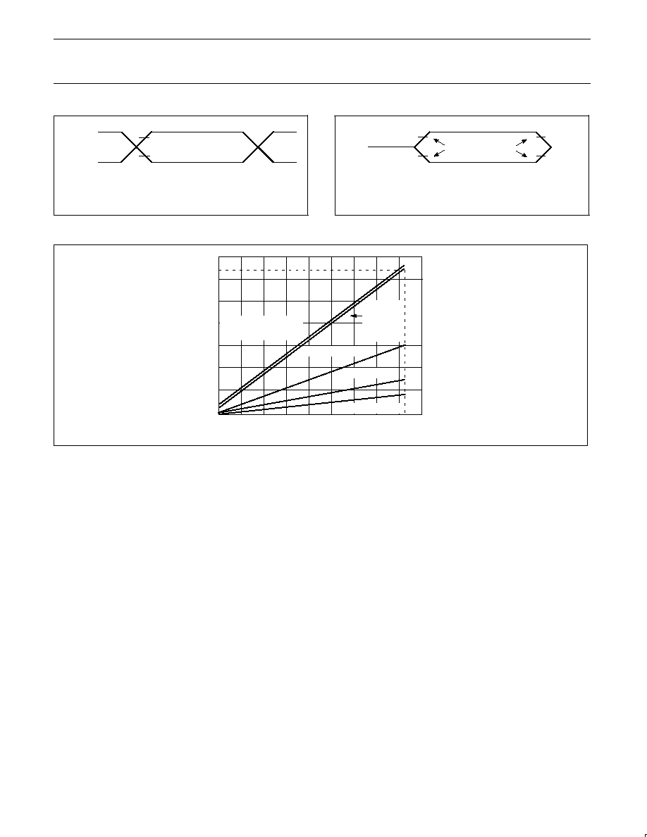
Philips Semiconductors
Product specification
8XC52/54/58/80C32
8XC51FA/FB/FC/80C51FA
8XC51RA+/RB+/RC+/RD+/80C51RA+
80C51 8-bit microcontroller family
8K≠64K/256≠1K OTP/ROM/ROMless, low voltage (2.7V≠5.5V),
low power, high speed (33MHz)
1999 Apr 01
42
VCC≠0.5
0.45V
0.2VCC+0.9
0.2VCC≠0.1
NOTE:
AC inputs during testing are driven at V
CC
≠0.5 for a logic `1' and 0.45V for a logic `0'.
Timing measurements are made at V
IH
min for a logic `1' and V
IL
max for a logic `0'.
SU00717
Figure 34. AC Testing Input/Output
VLOAD
VLOAD+0.1V
VLOAD≠0.1V
VOH≠0.1V
VOL+0.1V
NOTE:
TIMING
REFERENCE
POINTS
For timing purposes, a port is no longer floating when a 100mV change from
load voltage occurs, and begins to float when a 100mV change from the loaded
V
OH
/V
OL
level occurs. I
OH
/I
OL
±
20mA.
SU00718
Figure 35. Float Waveform
SU00837A
TYP ACTIVE MODE
MAX IDLE MODE
TYP IDLE MODE
MAX ACTIVE
MODE (EXCEPT
8XC51RD+)
I
CC
MAX = 0.9 X
FREQ. + 1.1
5
4
8
12
16
FREQ AT XTAL1 (MHz)
20
24
28
32
36
15
25
30
I CC
(mA)
10
20
35
I
CCMAX
ACTIVE MODE
(8XC51RD+)
I
CCMAX
= 0.9 X FREQ + 2.1
Figure 36. I
CC
vs. FREQ
Valid only within frequency specifications of the device under test

Philips Semiconductors
Product specification
8XC52/54/58/80C32
8XC51FA/FB/FC/80C51FA
8XC51RA+/RB+/RC+/RD+/80C51RA+
80C51 8-bit microcontroller family
8K≠64K/256≠1K OTP/ROM/ROMless, low voltage (2.7V≠5.5V),
low power, high speed (33MHz)
1999 Apr 01
43
V
CC
P0
EA
RST
XTAL1
XTAL2
V
SS
V
CC
V
CC
V
CC
I
CC
(NC)
CLOCK SIGNAL
SU00719
Figure 37. I
CC
Test Condition, Active Mode
All other pins are disconnected
V
CC
P0
EA
RST
XTAL1
XTAL2
V
SS
V
CC
V
CC
I
CC
(NC)
CLOCK SIGNAL
SU00720
Figure 38. I
CC
Test Condition, Idle Mode
All other pins are disconnected
VCC≠0.5
0.45V
0.7VCC
0.2VCC≠0.1
t
CHCL
t
CLCL
t
CLCH
t
CLCX
t
CHCX
SU00009
Figure 39. Clock Signal Waveform for I
CC
Tests in Active and Idle Modes
t
CLCH
= t
CHCL
= 5ns
V
CC
P0
EA
RST
XTAL1
XTAL2
VSS
V
CC
V
CC
I
CC
(NC)
SU00016
Figure 40. I
CC
Test Condition, Power Down Mode
All other pins are disconnected. V
CC
= 2V to 5.5V

Philips Semiconductors
Product specification
8XC52/54/58/80C32
8XC51FA/FB/FC/80C51FA
8XC51RA+/RB+/RC+/RD+/80C51RA+
80C51 8-bit microcontroller family
8K≠64K/256≠1K OTP/ROM/ROMless, low voltage (2.7V≠5.5V),
low power, high speed (33MHz)
1999 Apr 01
44
EPROM CHARACTERISTICS
All these devices can be programmed by using a modified Improved
Quick-Pulse Programming
TM
algorithm. It differs from older methods
in the value used for V
PP
(programming supply voltage) and in the
width and number of the ALE/PROG pulses.
The family contains two signature bytes that can be read and used
by an EPROM programming system to identify the device. The
signature bytes identify the device as being manufactured by
Philips.
Table 9 shows the logic levels for reading the signature byte, and for
programming the program memory, the encryption table, and the
security bits. The circuit configuration and waveforms for quick-pulse
programming are shown in Figures 41 and 42. Figure 43 shows the
circuit configuration for normal program memory verification.
Quick-Pulse Programming
The setup for microcontroller quick-pulse programming is shown in
Figure 41. Note that the device is running with a 4 to 6MHz
oscillator. The reason the oscillator needs to be running is that the
device is executing internal address and program data transfers.
The address of the EPROM location to be programmed is applied to
ports 1 and 2, as shown in Figure 41. The code byte to be
programmed into that location is applied to port 0. RST, PSEN and
pins of ports 2 and 3 specified in Table 9 are held at the `Program
Code Data' levels indicated in Table 9. The ALE/PROG is pulsed
low 5 times as shown in Figure 42.
To program the encryption table, repeat the 5 pulse programming
sequence for addresses 0 through 1FH, using the `Pgm Encryption
Table' levels. Do not forget that after the encryption table is
programmed, verification cycles will produce only encrypted data.
To program the security bits, repeat the 5 pulse programming
sequence using the `Pgm Security Bit' levels. After one security bit is
programmed, further programming of the code memory and
encryption table is disabled. However, the other security bits can still
be programmed.
Note that the EA/V
PP
pin must not be allowed to go above the
maximum specified V
PP
level for any amount of time. Even a narrow
glitch above that voltage can cause permanent damage to the
device. The V
PP
source should be well regulated and free of glitches
and overshoot.
Program Verification
If security bits 2 and 3 have not been programmed, the on-chip
program memory can be read out for program verification. The
address of the program memory locations to be read is applied to
ports 1 and 2 as shown in Figure 43. The other pins are held at the
`Verify Code Data' levels indicated in Table 9. The contents of the
address location will be emitted on port 0. External pull-ups are
required on port 0 for this operation.
If the 64 byte encryption table has been programmed, the data
presented at port 0 will be the exclusive NOR of the program byte
with one of the encryption bytes. The user will have to know the
encryption table contents in order to correctly decode the verification
data. The encryption table itself cannot be read out.
Reading the Signature Bytes
The signature bytes are read by the same procedure as a normal
verification of locations 030H and 031H, except that P3.6 and P3.7
need to be pulled to a logic low. The values are:
(030H) = 15H indicates manufactured by Philips
(031H) = 97H indicates 87C52
BBH indicates 87C54
BDH indicates 87C58
B1H indicates 87C51FA
B2H indicates 87C51FB
B3H indicates 87C51FC
CAH indicates 87C51RA+
CBH indicates 87C51RB+
CCH indicates 87C51RC+
CDH indicates 87C51RD+
(060H) = NA
Program/Verify Algorithms
Any algorithm in agreement with the conditions listed in Table 9, and
which satisfies the timing specifications, is suitable.
Security Bits
With none of the security bits programmed the code in the program
memory can be verified. If the encryption table is programmed, the
code will be encrypted when verified. When only security bit 1 (see
Table 10) is programmed, MOVC instructions executed from
external program memory are disabled from fetching code bytes
from the internal memory, EA is latched on Reset and all further
programming of the EPROM is disabled. When security bits 1 and 2
are programmed, in addition to the above, verify mode is disabled.
When all three security bits are programmed, all of the conditions
above apply and all external program memory execution is disabled.
Encryption Array
64 bytes of encryption array are initially unprogrammed (all 1s).
TM
Trademark phrase of Intel Corporation.
Philips Semiconductors
Product specification
8XC52/54/58/80C32
8XC51FA/FB/FC/80C51FA
8XC51RA+/RB+/RC+/RD+/80C51RA+
80C51 8-bit microcontroller family
8K≠64K/256≠1K OTP/ROM/ROMless, low voltage (2.7V≠5.5V),
low power, high speed (33MHz)
1999 Apr 01
45
Table 9. EPROM Programming Modes
MODE
RST
PSEN
ALE/PROG
EA/V
PP
P2.7
P2.6
P3.7
P3.6
Read signature
1
0
1
1
0
0
0
0
Program code data
1
0
0*
V
PP
1
0
1
1
Verify code data
1
0
1
1
0
0
1
1
Pgm encryption table
1
0
0*
V
PP
1
0
1
0
Pgm security bit 1
1
0
0*
V
PP
1
1
1
1
Pgm security bit 2
1
0
0*
V
PP
1
1
0
0
Pgm security bit 3
1
0
0*
V
PP
0
1
0
1
NOTES:
1. `0' = Valid low for that pin, `1' = valid high for that pin.
2. V
PP
= 12.75V
±
0.25V.
3. V
CC
= 5V
±
10% during programming and verification.
*
ALE/PROG receives 5 programming pulses for code data (also for user array; 5 pulses for encryption or security bits) while V
PP
is held at
12.75V. Each programming pulse is low for 100
µ
s (
±
10
µ
s) and high for a minimum of 10
µ
s.
Table 10. Program Security Bits for EPROM Devices
PROGRAM LOCK BITS
1, 2
SB1
SB2
SB3
PROTECTION DESCRIPTION
1
U
U
U
No Program Security features enabled. (Code verify will still be encrypted by the Encryption Array if
programmed.)
2
P
U
U
MOVC instructions executed from external program memory are disabled from fetching code bytes
from internal memory, EA is sampled and latched on Reset, and further programming of the EPROM
is disabled.
3
P
P
U
Same as 2, also verify is disabled.
4
P
P
P
Same as 3, external execution is disabled.
NOTES:
1. P ≠ programmed. U ≠ unprogrammed.
2. Any other combination of the security bits is not defined.
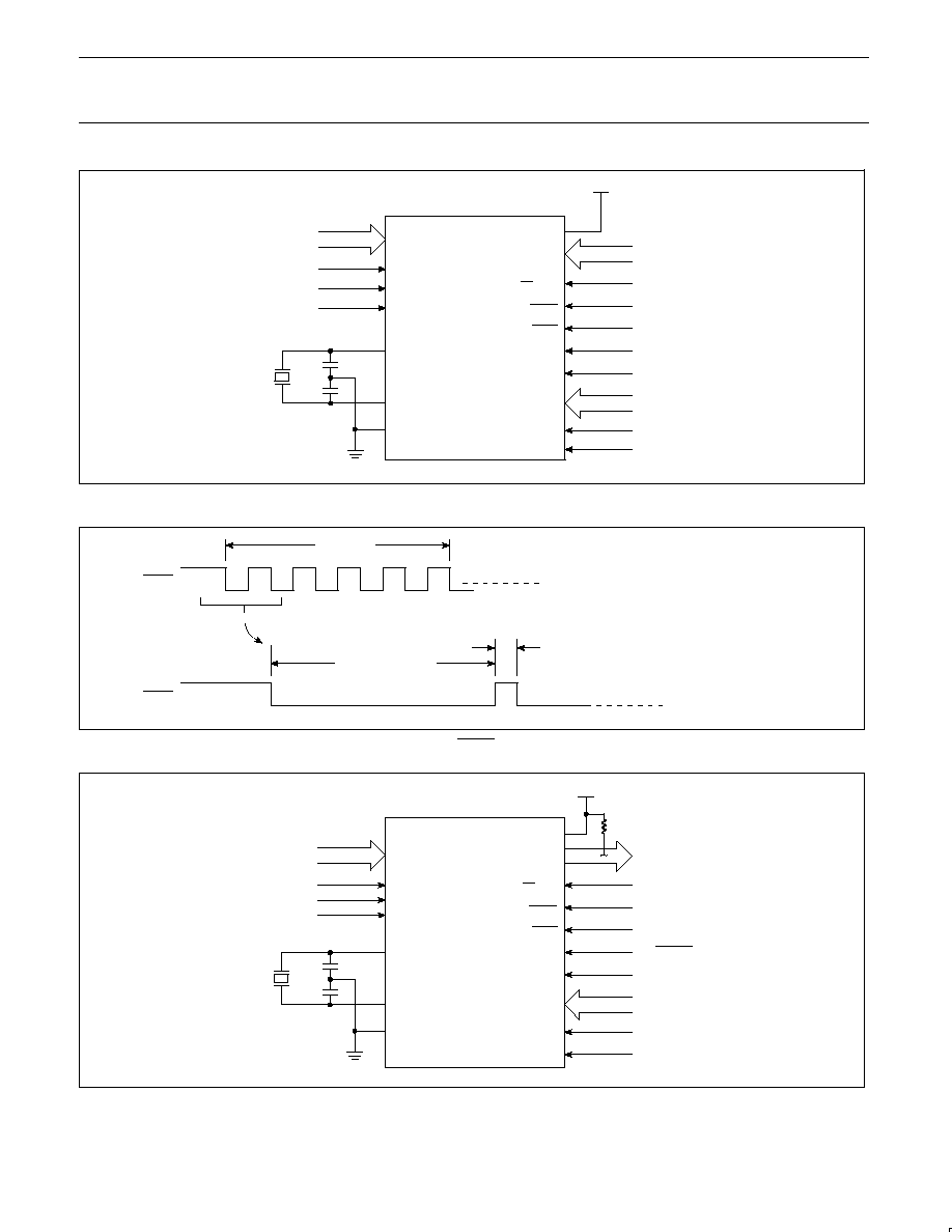
Philips Semiconductors
Product specification
8XC52/54/58/80C32
8XC51FA/FB/FC/80C51FA
8XC51RA+/RB+/RC+/RD+/80C51RA+
80C51 8-bit microcontroller family
8K≠64K/256≠1K OTP/ROM/ROMless, low voltage (2.7V≠5.5V),
low power, high speed (33MHz)
1999 Apr 01
46
A0≠A7
1
1
1
4≠6MHz
+5V
PGM DATA
+12.75V
5 PULSES TO GROUND
0
1
0
A8≠A13
P1
RST
P3.6
P3.7
XTAL2
XTAL1
VSS
VCC
P0
EA/VPP
ALE/PROG
PSEN
P2.7
P2.6
P2.0≠P2.5
OTP
A14
P3.4
SU00838A
P3.5
A8≠A15 are programming addresses
(not external memory addresses per
device pin out)
A15 (RD+ ONLY)
Figure 41. Programming Configuration
ALE/PROG:
ALE/PROG:
1
0
1
0
5 PULSES
t
GLGH
= 100
µ
s
±
10
µ
s
t
GHGL
= 10
µ
s MIN
SU00875
1
2
3
4
5
SEE EXPLODED VIEW BELOW
1
Figure 42. PROG Waveform
A0≠A7
1
1
1
+5V
PGM DATA
1
1
0
0 ENABLE
0
A8≠A13
P1
RST
P3.6
P3.7
XTAL2
XTAL1
VSS
VCC
P0
EA/VPP
ALE/PROG
PSEN
P2.7
P2.6
P2.0≠P2.5
OTP
A14
P3.4
SU00870
4≠6MHz
A8≠A15 are programming addresses
(not external memory addresses per
device pin out)
P3.5
A15 (RD+ ONLY)
Figure 43. Program Verification
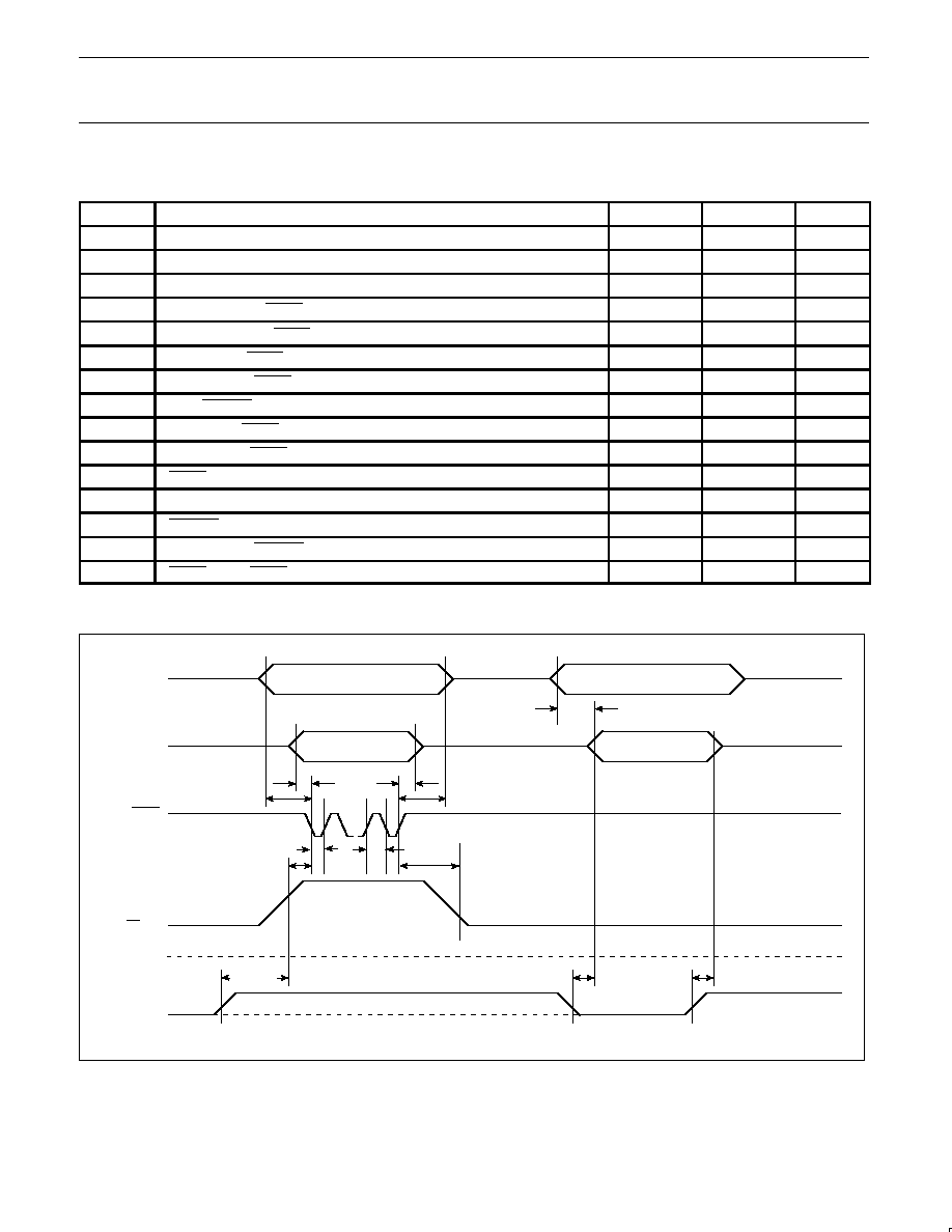
Philips Semiconductors
Product specification
8XC52/54/58/80C32
8XC51FA/FB/FC/80C51FA
8XC51RA+/RB+/RC+/RD+/80C51RA+
80C51 8-bit microcontroller family
8K≠64K/256≠1K OTP/ROM/ROMless, low voltage (2.7V≠5.5V),
low power, high speed (33MHz)
1999 Apr 01
47
EPROM PROGRAMMING AND VERIFICATION CHARACTERISTICS
T
amb
= 21
∞
C to +27
∞
C, V
CC
= 5V
±
10%, V
SS
= 0V (See Figure 44)
SYMBOL
PARAMETER
MIN
MAX
UNIT
V
PP
Programming supply voltage
12.5
13.0
V
I
PP
Programming supply current
50
1
mA
1/t
CLCL
Oscillator frequency
4
6
MHz
t
AVGL
Address setup to PROG low
48t
CLCL
t
GHAX
Address hold after PROG
48t
CLCL
t
DVGL
Data setup to PROG low
48t
CLCL
t
GHDX
Data hold after PROG
48t
CLCL
t
EHSH
P2.7 (ENABLE) high to V
PP
48t
CLCL
t
SHGL
V
PP
setup to PROG low
10
µ
s
t
GHSL
V
PP
hold after PROG
10
µ
s
t
GLGH
PROG width
90
110
µ
s
t
AVQV
Address to data valid
48t
CLCL
t
ELQZ
ENABLE low to data valid
48t
CLCL
t
EHQZ
Data float after ENABLE
0
48t
CLCL
t
GHGL
PROG high to PROG low
10
µ
s
NOTE:
1. Not tested.
PROGRAMMING
*
VERIFICATION
*
ADDRESS
ADDRESS
DATA IN
DATA OUT
LOGIC 1
LOGIC 1
LOGIC 0
t
AVQV
t
EHQZ
t
ELQV
t
SHGL
t
GHSL
t
GLGH
t
GHGL
t
AVGL
t
GHAX
t
DVGL
t
GHDX
P1.0≠P1.7
P2.0≠P2.5
P3.4
(A0 ≠ A14)
PORT 0
P0.0 ≠ P0.7
(D0 ≠ D7)
ALE/PROG
EA/V
PP
P2.7
**
SU00871
t
EHSH
NOTES:
*
FOR PROGRAMMING CONFIGURATION SEE FIGURE 41.
FOR VERIFICATION CONDITIONS SEE FIGURE 43.
**
SEE TABLE 9.
Figure 44. EPROM Programming and Verification
Philips Semiconductors
Product specification
8XC52/54/58/80C32
8XC51FA/FB/FC/80C51FA
8XC51RA+/RB+/RC+/RD+/80C51RA+
80C51 8-bit microcontroller family
8K≠64K/256≠1K OTP/ROM/ROMless, low voltage (2.7V≠5.5V),
low power, high speed (33MHz)
1999 Apr 01
48
MASK ROM DEVICES
Security Bits
With none of the security bits programmed the code in the program
memory can be verified. If the encryption table is programmed, the
code will be encrypted when verified. When only security bit 1 (see
Table 11) is programmed, MOVC instructions executed from external
program memory are disabled from fetching code bytes from the
internal memory, EA is latched on Reset and all further programming
of the EPROM is disabled. When security bits 1 and 2 are
programmed, in addition to the above, verify mode is disabled.
Encryption Array
64 bytes of encryption array are initially unprogrammed (all 1s).
Table 11. Program Security Bits
PROGRAM LOCK BITS
1, 2
SB1
SB2
PROTECTION DESCRIPTION
1
U
U
No Program Security features enabled.
(Code verify will still be encrypted by the Encryption Array if programmed.)
2
P
U
MOVC instructions executed from external program memory are disabled from fetching code bytes from
internal memory, EA is sampled and latched on Reset, and further programming of the EPROM is disabled.
NOTES:
1. P ≠ programmed. U ≠ unprogrammed.
2. Any other combination of the security bits is not defined.
ROM CODE SUBMISSION FOR 8K ROM DEVICES (80C52, 83C51FA, AND 83C51RA+)
When submitting ROM code for the 8k ROM devices, the following must be specified:
1. 8k byte user ROM data
2. 64 byte ROM encryption key
3. ROM security bits.
ADDRESS
CONTENT
BIT(S)
COMMENT
0000H to 1FFFH
DATA
7:0
User ROM Data
2000H to 203FH
KEY
7:0
ROM Encryption Key
FFH = no encryption
2040H
SEC
0
ROM Security Bit 1
0 = enable security
1 = disable security
2040H
SEC
1
ROM Security Bit 2
0 = enable security
1 = disable security
Security Bit 1:
When programmed, this bit has two effects on masked ROM parts:
1. External MOVC is disabled, and
2. EA is latched on Reset.
Security Bit 2:
When programmed, this bit inhibits Verify User ROM.
NOTE: Security Bit 2 cannot be enabled unless Security Bit 1 is enabled.
If the ROM Code file does not include the options, the following information must be included with the ROM code.
For each of the following, check the appropriate box, and send to Philips along with the code:
Security Bit #1:
V
Enabled
V
Disabled
Security Bit #2:
V
Enabled
V
Disabled
Encryption:
V
No
V
Yes
If Yes, must send key file.
Philips Semiconductors
Product specification
8XC52/54/58/80C32
8XC51FA/FB/FC/80C51FA
8XC51RA+/RB+/RC+/RD+/80C51RA+
80C51 8-bit microcontroller family
8K≠64K/256≠1K OTP/ROM/ROMless, low voltage (2.7V≠5.5V),
low power, high speed (33MHz)
1999 Apr 01
49
ROM CODE SUBMISSION FOR 16K ROM DEVICES (80C54, 83C51FB AND 83C51RB+)
When submitting ROM code for the 16K ROM devices, the following must be specified:
1. 16k byte user ROM data
2. 64 byte ROM encryption key
3. ROM security bits.
ADDRESS
CONTENT
BIT(S)
COMMENT
0000H to 3FFFH
DATA
7:0
User ROM Data
4000H to 403FH
KEY
7:0
ROM Encryption Key
FFH = no encryption
4040H
SEC
0
ROM Security Bit 1
0 = enable security
1 = disable security
4040H
SEC
1
ROM Security Bit 2
0 = enable security
1 = disable security
Security Bit 1: When programmed, this bit has two effects on masked ROM parts:
1. External MOVC is disabled, and
2. EA is latched on Reset.
Security Bit 2: When programmed, this bit inhibits Verify User ROM.
NOTE: Security Bit 2 cannot be enabled unless Security Bit 1 is enabled.
If the ROM Code file does not include the options, the following information must be included with the ROM code.
For each of the following, check the appropriate box, and send to Philips along with the code:
Security Bit #1:
V
Enabled
V
Disabled
Security Bit #2:
V
Enabled
V
Disabled
Encryption:
V
No
V
Yes
If Yes, must send key file.

Philips Semiconductors
Product specification
8XC52/54/58/80C32
8XC51FA/FB/FC/80C51FA
8XC51RA+/RB+/RC+/RD+/80C51RA+
80C51 8-bit microcontroller family
8K≠64K/256≠1K OTP/ROM/ROMless, low voltage (2.7V≠5.5V),
low power, high speed (33MHz)
1999 Apr 01
50
ROM CODE SUBMISSION FOR 32K ROM DEVICES (80C58, 83C51FC, AND 83C51RC+)
When submitting ROM code for the 32K ROM devices, the following must be specified:
1. 32k byte user ROM data
2. 64 byte ROM encryption key
3. ROM security bits.
ADDRESS
CONTENT
BIT(S)
COMMENT
0000H to 7FFFH
DATA
7:0
User ROM Data
8000H to 803FH
KEY
7:0
ROM Encryption Key
FFH = no encryption
8040H
SEC
0
ROM Security Bit 1
0 = enable security
1 = disable security
8040H
SEC
1
ROM Security Bit 2
0 = enable security
1 = disable security
Security Bit 1: When programmed, this bit has two effects on masked ROM parts:
1. External MOVC is disabled, and
2. EA is latched on Reset.
Security Bit 2: When programmed, this bit inhibits Verify User ROM.
NOTE: Security Bit 2 cannot be enabled unless Security Bit 1 is enabled.
If the ROM Code file does not include the options, the following information must be included with the ROM code.
For each of the following, check the appropriate box, and send to Philips along with the code:
Security Bit #1:
V
Enabled
V
Disabled
Security Bit #2:
V
Enabled
V
Disabled
Encryption:
V
No
V
Yes
If Yes, must send key file.

Philips Semiconductors
Product specification
8XC52/54/58/80C32
8XC51FA/FB/FC/80C51FA
8XC51RA+/RB+/RC+/RD+/80C51RA+
80C51 8-bit microcontroller family
8K≠64K/256≠1K OTP/ROM/ROMless, low voltage (2.7V≠5.5V),
low power, high speed (33MHz)
1999 Apr 01
51
ROM CODE SUBMISSION FOR 64K ROM DEVICE (83C51RD+)
When submitting ROM code for the 64K ROM devices, the following must be specified:
1. 64k byte user ROM data
2. 64 byte ROM encryption key
3. ROM security bits.
ADDRESS
CONTENT
BIT(S)
COMMENT
0000H to FFFFH
DATA
7:0
User ROM Data
10000H to 1003FH
KEY
7:0
ROM Encryption Key
FFH = no encryption
10040H
SEC
0
ROM Security Bit 1
0 = enable security
1 = disable security
10040H
SEC
1
ROM Security Bit 2
0 = enable security
1 = disable security
Security Bit 1: When programmed, this bit has two effects on masked ROM parts:
1. External MOVC is disabled, and
2. EA is latched on Reset.
Security Bit 2: When programmed, this bit inhibits Verify User ROM.
NOTE: Security Bit 2 cannot be enabled unless Security Bit 1 is enabled.
If the ROM Code file does not include the options, the following information must be included with the ROM code.
For each of the following, check the appropriate box, and send to Philips along with the code:
Security Bit #1:
V
Enabled
V
Disabled
Security Bit #2:
V
Enabled
V
Disabled
Encryption:
V
No
V
Yes
If Yes, must send key file.
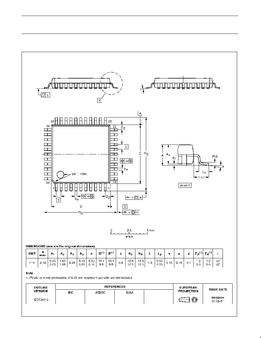
Philips Semiconductors
Product specification
8XC52/54/58/80C32
8XC51FA/FB/FC/80C51FA
8XC51RA+/RB+/RC+/RD+/80C51RA+
80C51 8-bit microcontroller family
8K≠64K/256≠1K OTP/ROM/ROMless, low voltage (2.7V≠5.5V),
low power, high speed (33MHz)
1999 Apr 01
52
QFP44:
plastic quad flat package; 44 leads (lead length 1.3 mm); body 10 x 10 x 1.75 mm
SOT307-2
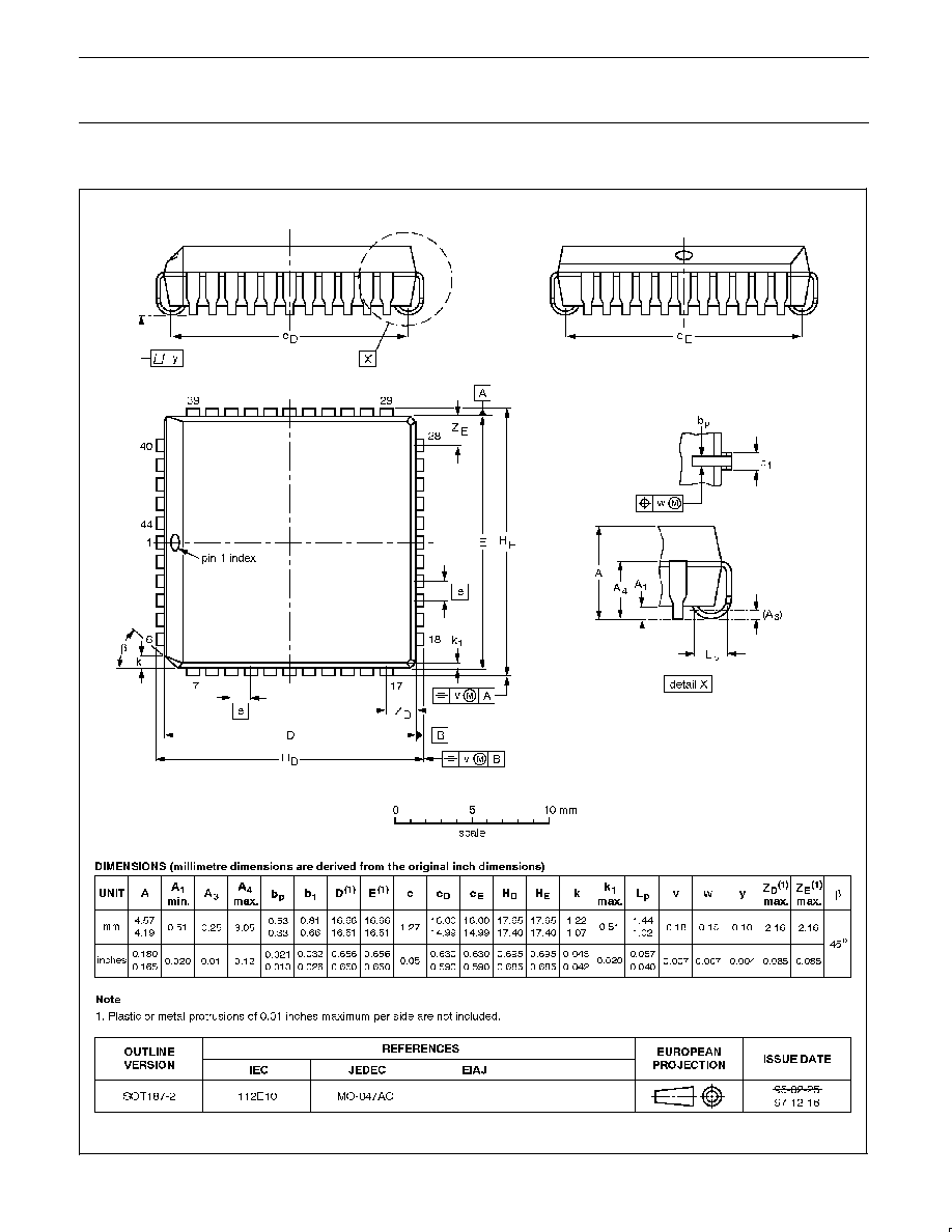
Philips Semiconductors
Product specification
8XC52/54/58/80C32
8XC51FA/FB/FC/80C51FA
8XC51RA+/RB+/RC+/RD+/80C51RA+
80C51 8-bit microcontroller family
8K≠64K/256≠1K OTP/ROM/ROMless, low voltage (2.7V≠5.5V),
low power, high speed (33MHz)
1999 Apr 01
53
PLCC44:
plastic leaded chip carrier; 44 leads
SOT187-2
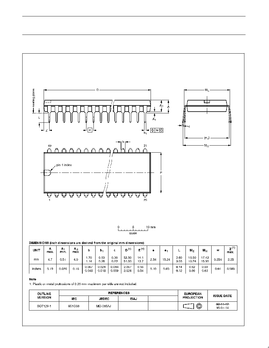
Philips Semiconductors
Product specification
8XC52/54/58/80C32
8XC51FA/FB/FC/80C51FA
8XC51RA+/RB+/RC+/RD+/80C51RA+
80C51 8-bit microcontroller family
8K≠64K/256≠1K OTP/ROM/ROMless, low voltage (2.7V≠5.5V),
low power, high speed (33MHz)
1999 Apr 01
54
DIP40:
plastic dual in-line package; 40 leads (600 mil)
SOT129-1

Philips Semiconductors
Product specification
8XC52/54/58/80C32
8XC51FA/FB/FC/80C51FA
8XC51RA+/RB+/RC+/RD+/80C51RA+
80C51 8-bit microcontroller family
8K≠64K/256≠1K OTP/ROM/ROMless, low voltage (2.7V≠5.5V),
low power, high speed (33MHz)
1999 Apr 01
55
NOTES

Philips Semiconductors
Product specification
8XC52/54/58/80C32
8XC51FA/FB/FC/80C51FA
8XC51RA+/RB+/RC+/RD+/80C51RA+
80C51 8-bit microcontroller family
8K≠64K/256≠1K OTP/ROM/ROMless, low voltage (2.7V≠5.5V),
low power, high speed (33MHz)
1999 Apr 01
56
Definitions
Short-form specification -- The data in a short-form specification is extracted from a full data sheet with the same type number and title. For
detailed information see the relevant data sheet or data handbook.
Limiting values definition -- Limiting values given are in accordance with the Absolute Maximum Rating System (IEC 134). Stress above one
or more of the limiting values may cause permanent damage to the device. These are stress ratings only and operation of the device at these or
at any other conditions above those given in the Characteristics sections of the specification is not implied. Exposure to limiting values for extended
periods may affect device reliability.
Application information -- Applications that are described herein for any of these products are for illustrative purposes only. Philips
Semiconductors make no representation or warranty that such applications will be suitable for the specified use without further testing or
modification.
Disclaimers
Life support -- These products are not designed for use in life support appliances, devices or systems where malfunction of these products can
reasonably be expected to result in personal injury. Philips Semiconductors customers using or selling these products for use in such applications
do so at their own risk and agree to fully indemnify Philips Semiconductors for any damages resulting from such application.
Right to make changes -- Philips Semiconductors reserves the right to make changes, without notice, in the products, including circuits, standard
cells, and/or software, described or contained herein in order to improve design and/or performance. Philips Semiconductors assumes no
responsibility or liability for the use of any of these products, conveys no license or title under any patent, copyright, or mask work right to these
products, and makes no representations or warranties that these products are free from patent, copyright, or mask work right infringement, unless
otherwise specified.
Philips Semiconductors
811 East Arques Avenue
P.O. Box 3409
Sunnyvale, California 94088≠3409
Telephone 800-234-7381
©
Copyright Philips Electronics North America Corporation 1999
All rights reserved. Printed in U.S.A.
Date of release: 04-99
Document order number:
9397 750 05509
Philips
Semiconductors
Data sheet
status
Objective
specification
Preliminary
specification
Product
specification
Product
status
Development
Qualification
Production
Definition
[1]
This data sheet contains the design target or goal specifications for product development.
Specification may change in any manner without notice.
This data sheet contains preliminary data, and supplementary data will be published at a later date.
Philips Semiconductors reserves the right to make chages at any time without notice in order to
improve design and supply the best possible product.
This data sheet contains final specifications. Philips Semiconductors reserves the right to make
changes at any time without notice in order to improve design and supply the best possible product.
Data sheet status
[1]
Please consult the most recently issued datasheet before initiating or completing a design.