 | –≠–ª–µ–∫—Ç—Ä–æ–Ω–Ω—ã–π –∫–æ–º–ø–æ–Ω–µ–Ω—Ç: 83C562 | –°–∫–∞—á–∞—Ç—å:  PDF PDF  ZIP ZIP |
Philips
Semiconductors
80C562/83C562
Single-chip 8-bit microcontroller
Product specification
1992 Jan 08
INTEGRATED CIRCUITS
IC20 Data Handbook
Philips Semiconductors
Product specification
80C562/83C562
Single-chip 8-bit microcontroller
Single-chip 8-bit microcontroller with 8-bit A/D, capture/compare timer, high-speed outputs, PWM
2
1992 Jan 08
853≠1463 05128
DESCRIPTION
The 80C562/83C562 (hereafter generically
referred to as 8XC562) Single-Chip 8-Bit
Microcontroller is manufactured in an
advanced CMOS process and is a derivative
of the 80C51 microcontroller family. The
83C562/83C562 has the same instruction set
as the 80C51.
The 8XC562 contains a non-volatile 256
◊
8
read-only program memory, a volatile 256
◊
8
read/write data memory (83C562) (the
80C562 is ROMless), a volatile 256
◊
8
read/write data memory, six 8-bit I/O ports,
two 16-bit timer/event counters (identical to
the timers of the 80C51), an additional 16-bit
timer coupled to capture and compare
latches, a 15-source, two-priority-level,
nested interrupt structure, an 8-input ADC,
two pulse width modulated outputs, standard
80C51 UART, a "watchdog" timer and on-chip
oscillator and timing circuits. For systems that
require extra capability, the 83C562 can be
expanded using standard TTL compatible
memories and logic.
The device also functions as an arithmetic
processor having facilities for both binary and
BCD arithmetic plus bit-handling capabilities.
The instruction set consists of over 100
instructions: 49 one-byte, 45 two-byte and 17
three-byte. With a 12MHz crystal, 58% of the
instructions are executed in 1
µ
s and 40% in
2
µ
s. Multiply and divide instructions require
4
µ
s.
FEATURES
∑
80C51 instruction set
∑
8k
◊
8 ROM expandable externally to
64k bytes
∑
256
◊
8 RAM, expandable externally to
64k bytes
∑
Two standard 16-bit timer/counters
∑
An additional 16-bit timer/counter coupled
to four capture registers and three compare
registers
∑
Capable of producing eight synchronized,
timed outputs
∑
An 8-bit ADC with eight multiplexed analog
inputs
∑
Two 8-bit resolution, pulse width modulated
outputs
∑
Five 8-bit I/O ports plus one 8-bit input port
shared with analog inputs
∑
Full-duplex UART compatible with the
standard 80C51
∑
On-chip watchdog timer
∑
Three temperature ranges
≠ 0 to +70
∞
C
≠ ≠40 to +85
∞
C
≠ ≠40 to +125
∞
C
PIN CONFIGURATION
Pin
Function
1
P5.0/ADC0
2
V
DD
3
STADC
4
PWM0
5
PWM1
6
EW
7
P4.0/CMSR0
8
P4.1/CMSR1
9
P4.2/CMSR2
10
P4.3/CMSR3
11
P4.4/CMSR4
12
P4.5/CMSR5
13
P4.6/CMT0
14
P4.7/CMT1
15
RST
16
P1.0/CT0I
17
P1.1/CT1I
18
P1.2/CT2I
19
P1.3/CT3I
20
P1.4/T2
21
P1.5/RT2
22
P1.6
23
P1.7
24
P3.0/RxD
25
P3.1/TxD
26
P3.2/INT0
27
P3.3/INT1
28
P3.4/T0
29
P3.5/T1
30
P3.6/WR
31
P3.7/RD
32
NC
33
NC
34
XTAL2
Pin
Function
35
XTAL1
36
V
SS
37
V
SS
38
NC
39
P2.0/A08
40
P2.1/A09
41
P2.2/A10
42
P2.3/A11
43
P2.4/A12
44
P2.5/A13
45
P2.6/A14
46
P2.7/A15
47
PSEN
48
ALE
49
EA
50
P0.7/AD7
51
P0.6/AD6
52
P0.5/AD5
53
P0.4/AD4
54
P0.3/AD3
55
P0.2/AD2
56
P0.1/AD1
57
P0.0/AD0
58
AVref≠
59
AVref+
60
AV
SS
61
AV
DD
62
P5.7/ADC7
63
P5.6/ADC6
64
P5.5/ADC5
65
P5.4/ADC4
66
P5.3/ADC3
67
P5.2/ADC2
68
P5.1/ADC1
SU00224
9
1
61
60
44
43
27
26
10
PLASTIC
LEADED
CHIP CARRIER
Philips Semiconductors
Product specification
80C562/83C562
Single-chip 8-bit microcontroller
1992 Jan 08
3
ORDERING INFORMATION
PHILIPS PART
ORDER NUMBER
PART MARKING
PHILIPS NORTH AMERICA
PART ORDER NUMBER
TEMPERATURE
RANGE
∞
C
ROMless
ROM
ROMless
ROM
Drawing
Number
EPROM
Drawing
Number
AND PACKAGE
FREQ
MHz
PCB80C562-
16WP
PCB83C562-
16WP/xxx
S80C562-4A68
S83C562-4A68
SOT188
S87C552-4A68
2
SOT188-3
0 to +70, Plastic
Leaded Chip Carrier
16
S87C552-4K68
2
1473A
0 to +70, Plastic
Leaded Chip Carrier
w/Window
16
PCF80C562-
12WP
PCF83C562-
12WP/xxx
S80C562-2A68
S83C562-2A68
SOT188
S87C552-5A68
2
SOT188-3
≠40 to +85, Plastic
Leaded Chip
Carrier
12
S87C552-5K68
2
1473A
≠40 to +85, Plastic
Leaded Chip Carrier
w/Window
12
PCA80C562-
12WP
PCA83C562-
12WP/xxx
S80C562-6A68
S83C562-6A68
SOT188
≠40 to +125, Plastic
Leaded Chip Carrier
12
NOTES:
1. 80C562 and 83C562 frequency range is 1.2MHz≠12MHz or 1.2MHz≠16MHz.
2. 87C552 frequency range is 3.5MHz≠16MHz. For full specification, see the 87C552 data sheets.
3. xxx denotes the ROM code number.
LOGIC SYMBOL
POR
T
5
POR
T
4
ADC0-7
CMT0
CMT1
CMSR0-5
RST
EW
XTAL1
XTAL2
EA
ALE
PSEN
AVref+
AVref≠
STADC
PWM0
PWM1
POR
T
0
LOW ORDER
ADDRESS AND
DATA BUS
POR
T
1
POR
T
2
POR
T
3
CT0I
CT1I
CT2I
CT3I
T2
RT2
RxD
TxD
INT0
INT1
T0
T1
WR
RD
VSS
VDD
AVSS
AVDD
HIGH ORDER
ADDRESS AND
DATA BUS
SU00225
Philips Semiconductors
Product specification
80C562/83C562
Single-chip 8-bit microcontroller
1992 Jan 08
4
BLOCK DIAGRAM
CPU
DUAL
PWM
ADC
8-BIT
PORT
80C51 CORE
EXCLUDING
ROM/RAM
8-BIT INTERNAL BUS
16
P0
P1
P2
P3
TxD
RxD
P5
P4
CT0I≠CT3I
T2
RT2
CMSR0≠CMSR5
CMT0, CMT1
RST
EW
XTAL1
XTAL2
EA
ALE
PSEN
WR
RD
T0
T1
INT0
INT1
VDD
VSS
PWM0
PWM1
AVSS
AVDD
AVREF
≠ +
STADC
ADC0≠7
3
3
3
3
3
3
0
2
1
1
1
4
5
0
1
2
ALTERNATE FUNCTION OF PORT 0
3
4
5
AD0≠7
A8≠15
3
3
16
PROGRAM
MEMORY
8k x 8 ROM
(83C562)
T0, T1
TWO 16-BIT
TIMER/EVENT
COUNTERS
DATA
MEMORY
256 x 8 RAM
PARALLEL I/O
PORTS AND
EXTERNAL BUS
SERIAL
UART
PORT
FOUR
16-BIT
CAPTURE
LATCHES
T2
16-BIT
TIMER/
EVENT
COUNTERS
T2
16-BIT
COMPARATORS
WITH
REGISTERS
COMPARATOR
OUTPUT
SELECTION
T3
WATCHDOG
TIMER
ALTERNATE FUNCTION OF PORT 1
ALTERNATE FUNCTION OF PORT 2
ALTERNATE FUNCTION OF PORT 3
ALTERNATE FUNCTION OF PORT 4
ALTERNATE FUNCTION OF PORT 5
SU00226
Philips Semiconductors
Product specification
80C562/83C562
Single-chip 8-bit microcontroller
1992 Jan 08
5
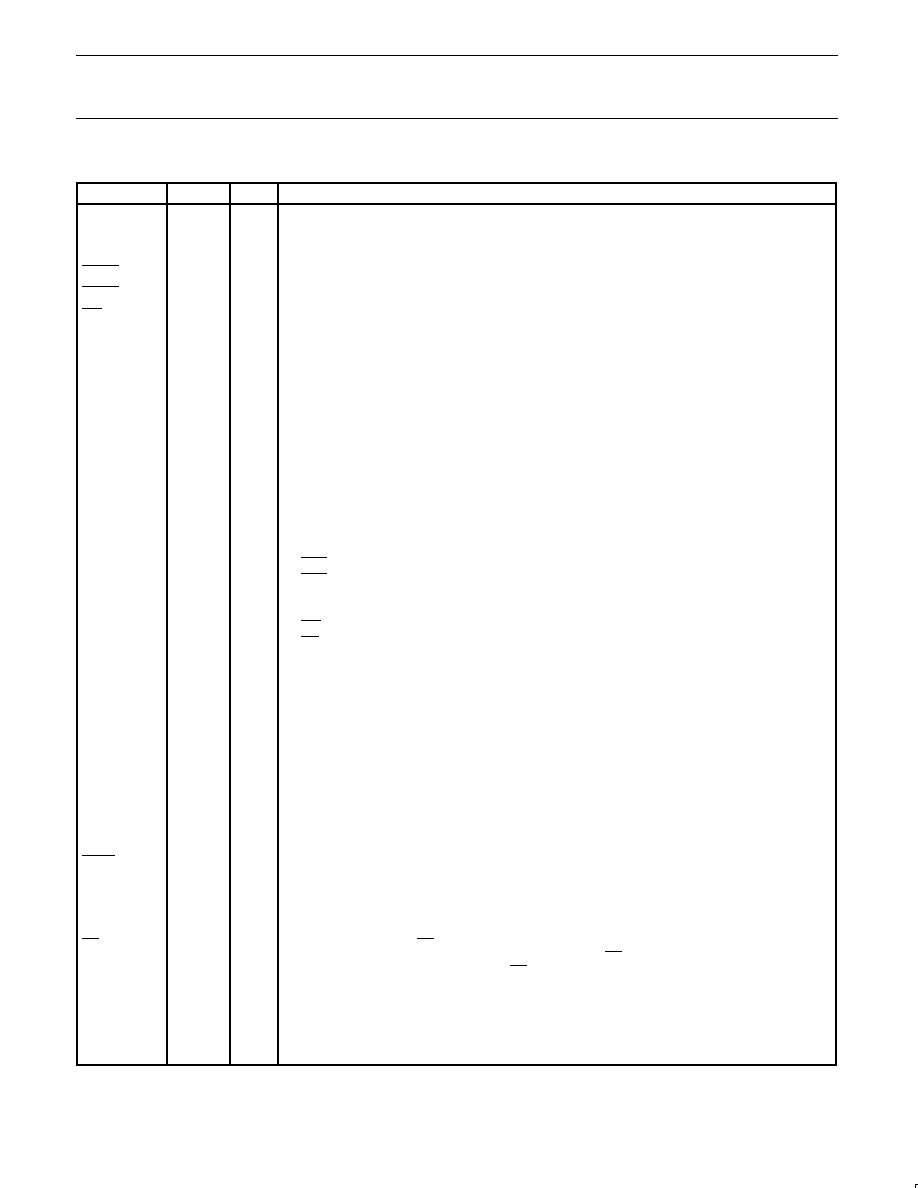
PIN DESCRIPTION
MNEMONIC
PIN NO.
TYPE
NAME AND FUNCTION
V
DD
2
I
Digital Power Supply: +5V power supply pin during normal operation, idle and power-down mode.
STADC
3
I
Start ADC Operation: Input starting analog to digital conversion (ADC operation can also be started
by software).
PWM0
4
O
Pulse Width Modulation: Output 0.
PWM1
5
O
Pulse Width Modulation: Output 1.
EW
6
I
Enable Watchdog Timer: Enable for T3 watchdog timer and disable power-down mode.
P0.0≠P0.7
57≠50
I/O
Port 0: Port 0 is an 8-bit open-drain bidirectional I/O port. Port 0 pins that have 1s written to them float
and can be used as high-impedance inputs. Port 0 is also the multiplexed low-order address and data
bus during accesses to external program and data memory. In this application it uses strong internal
pull-ups when emitting 1s.
P1.0≠P1.7
16≠23
I/O
Port 1: 8-bit I/O port. Alternate functions include:
16≠23
I/O
(P1.0≠P1.7): Quasi-bidirectional port pins.
16≠19
I/O
CT0I≠CT3I (P1.0≠P1.3): Capture timer input signals for timer T2.
20
I
T2 (P1.4): T2 event input
21
I
RT2 (P1.5): T2 timer reset signal. Rising edge triggered.
P2.0≠P2.7
39≠46
I/O
Port 2: 8-bit quasi-bidirectional I/O port.
Alternate function: High-order address byte for external memory (A08≠A15).
P3.0≠P3.7
24≠31
I/O
Port 3: 8-bit quasi-bidirectional I/O port. Alternate functions include:
24
RxD(P3.0): Serial input port.
25
TxD (P3.1): Serial output port.
26
INT0 (P3.2): External interrupt.
27
INT1 (P3.3): External interrupt.
28
T0 (P3.4): Timer 0 external input.
29
T1 (P3.5): Timer 1 external input.
30
WR (P3.6): External data memory write strobe.
31
RD (P3.7): External data memory read strobe.
P4.0≠P4.7
7≠14
I/O
Port 4: 8-bit quasi-bidirectional I/O port. Alternate functions include:
7≠12
O
CMSR0≠CMSR5 (P4.0≠P4.5): Timer T2 compare and set/reset outputs on a match with timer T2.
13, 14
O
CMT0, CMT1 (P4.6, P4.7): Timer T2 compare and toggle outputs on a match with timer T2.
P5.0≠P5.7
68≠62,
1
I
Port 5: 8-bit input port.
ADC0≠ADC7 (P5.0≠P5.7): Alternate function: Eight input channels to ADC.
RST
15
I/O
Reset: Input to reset the 87C552. It also provides a reset pulse as output when timer T3 overflows.
XTAL1
35
I
Crystal Input 1: Input to the inverting amplifier that forms the oscillator, and input to the internal clock
generator. Receives the external clock signal when an external oscillator is used.
XTAL2
34
O
Crystal Input 2: Output of the inverting amplifier that forms the oscillator. Left open≠circuit when an
external clock is used.
V
SS
36, 37
I
Digital ground.
PSEN
47
O
Program Store Enable: Active-low read strobe to external program memory.
ALE
48
O
Address Latch Enable: Latches the low byte of the address during accesses to external memory. It is
activated every six oscillator periods. During an external data memory access, one ALE pulse is
skipped. ALE can drive up to eight LS TTL inputs and handles CMOS inputs without an external
pull-up.
EA
49
I
External Access: When EA is held at TTL level high, the CPU executes out of the internal program
ROM provided the program counter is less than 8192. When EA is held at TTL low level, the CPU
executes out of external program memory. EA is not allowed to float.
AV
REF≠
58
I
Analog to Digital Conversion Reference Resistor: Low-end.
AV
REF+
59
I
Analog to Digital Conversion Reference Resistor: High-end.
AV
SS
60
I
Analog Ground
AV
DD
61
I
Analog Power Supply
NOTE:
1. To avoid "latch-up" effect at power-on, the voltage on any pin at any time must not be higher or lower than V
DD
+0.5V or V
SS
≠ 0.5V,
respectively.
Philips Semiconductors
Product specification
80C562/83C562
Single-chip 8-bit microcontroller
1992 Jan 08
6
OSCILLATOR
CHARACTERISTICS
XTAL1 and XTAL2 are the input and output,
respectively, of an inverting amplifier. The
pins can be configured for use as an on-chip
oscillator, as shown in the logic symbol.
To drive the device from an external clock
source, XTAL1 should be driven while XTAL2
is left unconnected. There are no
requirements on the duty cycle of the
external clock signal, because the input to
the internal clock circuitry is through a
divide-by-two flip-flop. However, minimum
and maximum high and low times specified in
the data sheet must be observed.
RESET
A reset is accomplished by holding the RST
pin high for at least two machine cycles (24
oscillator periods), while the oscillator is
running. To ensure a good power-on reset,
the RST pin must be high long enough to
allow the oscillator time to start up (normally
a few milliseconds) plus two machine cycles.
At power-on, the voltage on V
DD
and RST
must come up at the same time for a proper
start-up.
IDLE MODE
In the idle mode, the CPU puts itself to sleep
while all of the on-chip peripherals stay
active. The instruction to invoke the idle
mode is the last instruction executed in the
normal operating mode before the idle mode
is activated. The CPU contents, the on-chip
RAM, and all of the special function registers
remain intact during this mode. The idle
mode can be terminated either by any
enabled interrupt (at which time the process
is picked up at the interrupt service routine
and continued), or by a hardware reset which
starts the processor in the same manner as a
power-on reset.
POWER-DOWN MODE
In the power-down mode, the oscillator is
stopped and the instruction to invoke
power-down is the last instruction executed.
Only the contents of the on-chip RAM are
preserved. A hardware reset is the only way
to terminate the power-down mode. the
control bits for the reduced power modes are
in the special function register PCON. Table 1
shows the state of the I/O ports during low
current operating modes.
Table 1.
External Pin Status During Idle and Power-Down Modes
MODE
PROGRAM
MEMORY
ALE
PSEN
PORT 0
PORT 1
PORT 2
PORT 3
PORT 4
PWM0/
PWM1
Idle
Internal
1
1
Data
Data
Data
Data
Data
High
Idle
External
1
1
Float
Data
Address
Data
Data
High
Power-down
Internal
0
0
Data
Data
Data
Data
Data
High
Power-down
External
0
0
Float
Data
Data
Data
Data
High
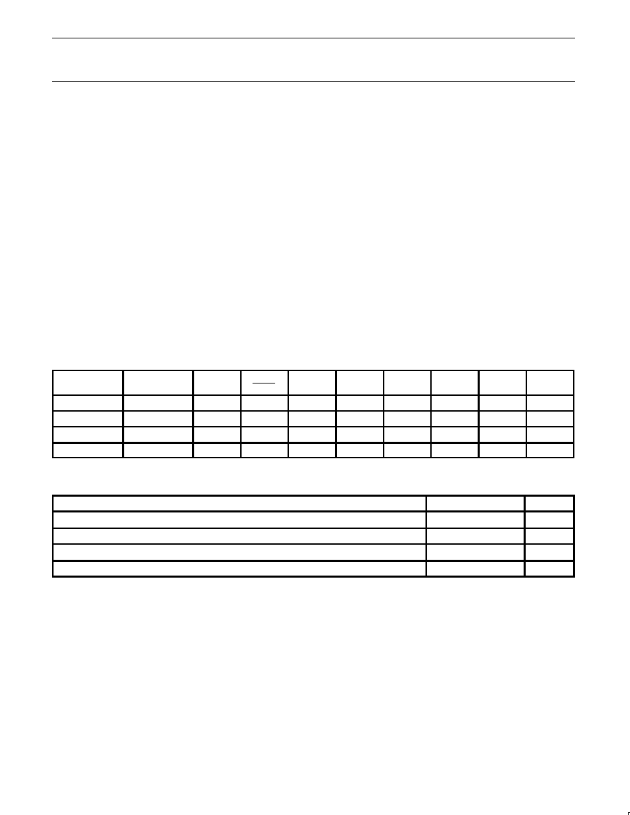
ABSOLUTE MAXIMUM RATINGS
1, 2, 3
PARAMETER
RATING
UNIT
Voltage on any other pin to V
SS
≠0.5 to +6.5
V
Input, output DC current on any single I/O pin
5.0
mA
Power dissipation (based on package heat transfer limitations, not device power consumption)
1.0
W
Storage temperature range
≠65 to +150
∞
C
NOTES:
1. Stresses above those listed under Absolute Maximum Ratings may cause permanent damage to the device. This is a stress rating only and
functional operation of the device at these or any conditions other than those described in the AC and DC Electrical Characteristics section
of this specification is not implied.
2. This product includes circuitry specifically designed for the protection of its internal devices from the damaging effects of excessive static
charge. Nonetheless, it is suggested that conventional precautions be taken to avoid applying greater than the rated maxima.
3. Parameters are valid over operating temperature range unless otherwise specified. All voltages are with respect to V
SS
unless otherwise
noted.
Philips Semiconductors
Product specification
80C562/83C562
Single-chip 8-bit microcontroller
1992 Jan 08
7
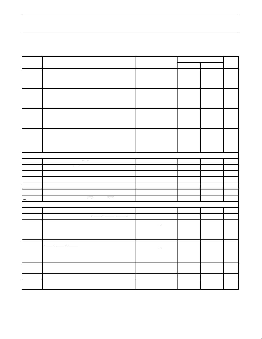
DC ELECTRICAL CHARACTERISTICS
V
SS
, AV
SS
= 0V
TEST
LIMITS
SYMBOL
PARAMETER
CONDITIONS
MIN
MAX
UNIT
V
DD
Supply voltage
PCB8XC562
4.0
6.0
V
PCF8XC562
4.0
6.0
V
PCA8XC562
4.5
5.5
V
I
DD
Supply current operating:
See notes 1 and 2
PCB8XC562
f
OSC
= 16MHz
45
mA
PCF8XC562
f
OSC
= 12MHz
34
mA
PCA8XC562
f
OSC
= 12MHz
30
mA
I
ID
Idle mode:
See notes 1 and 3
PCB8XC562
f
OSC
= 16MHz
10
mA
PCF8XC562
f
OSC
= 12MHz
8
mA
PCA8XC562
f
OSC
= 12MHz
7
mA
I
PD
Power-down current:
See notes 1 and 4;
2V < V
PD
< V
DD
max
PCB8XC562
50
µ
A
PCF8XC562
50
µ
A
PCA8XC562
100
µ
A
Inputs
V
IL
Input low voltage, except EA
≠0.5
0.2V
DD
≠0.1
V
V
IL1
Input low voltage to EA
≠0.5
0.2V
DD
≠0.3
V
V
IH
Input high voltage, except XTAL1, RST
0.2V
DD
+0.9
V
DD
+0.5
V
V
IH1
Input high voltage, XTAL1, RST
0.7V
DD
V
DD
+0.5
V
I
IL
Logical 0 input current, ports 1, 2, 3, 4
V
IN
= 0.45V
≠50
µ
A
I
TL
Logical 1-to-0 transition current, ports 1, 2, 3, 4
See note 5
≠650
µ
A
+I
IL1
Input leakage current, port 0, EA, STADC, EW
0.45V < V
I
< V
DD
10
µ
A
Outputs
V
OL
Output low voltage, ports 1, 2, 3, 4
I
OL
= 1.6mA
6
0.45
V
V
OL1
Output low voltage, port 0, ALE, PSEN, PWM0, PWM1
I
OL
= 3.2mA
6
0.45
V
V
OH
Output high voltage, ports 1, 2, 3, 4
V
DD
+ 5V+10%
≠I
OH
= 60
µ
A
2.4
V
≠I
OH
= 25
µ
A
0.75V
DD
V
≠I
OH
= 10
µ
A
0.9V
DD
V
V
OH1
Output high voltage (port 0 in external bus mode, ALE,
PSEN, PWM0, PWM1)
7
V
DD
+ 5V+10%
≠I
OH
= 400
µ
A
2.4
V
≠I
OH
= 150
µ
A
0.75V
DD
V
≠I
OH
= 40
µ
A
0.9V
DD
V
V
OH2
Output high voltage (RST)
≠I
OH
= 400
µ
A
2.4
V
≠I
OH
= 120
µ
A
0.8V
DD
V
R
RST
Internal reset pull-down resistor
50
150
k
C
IO
Pin capacitance
Test freq = 1MHz,
T
amb
= 25
∞
C
10
pF
Philips Semiconductors
Product specification
80C562/83C562
Single-chip 8-bit microcontroller
1992 Jan 08
8
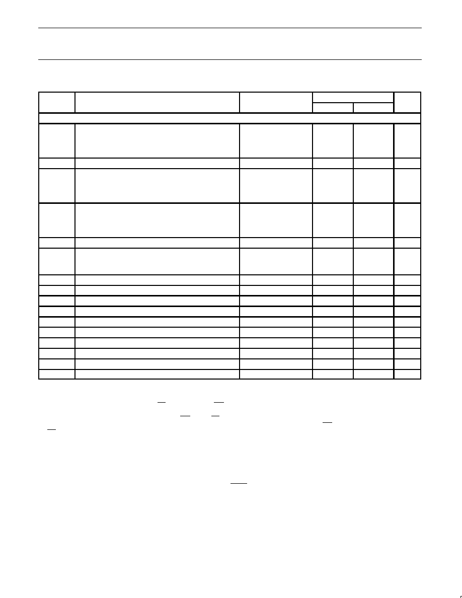
DC ELECTRICAL CHARACTERISTICS (Continued)
TEST
LIMITS
SYMBOL
PARAMETER
CONDITIONS
MIN
MAX
UNIT
Analog Inputs
AV
DD
Analog supply voltage:
PCB8XC562
AV
DD
= V
DD
±
0.2V
4.0
6.0
V
PCF8XC562
AV
DD
= V
DD
±
0.2V
4.0
6.0
V
PCA8XC562
AV
DD
= V
DD
±
0.2V
4.5
5.5
V
AI
DD
Analog supply current: operating:
Port 5 = 0 to AV
DD
1.2
mA
AI
ID
Idle mode:
PCB8XC562
50
µ
A
PCF8XC562
50
µ
A
PCA8XC562
100
µ
A
AI
PD
Power-down mode:
2V < AV
PD
< AV
DD
max
PCB8XC562
50
µ
A
PCF8XC562
50
µ
A
PCA8XC562
100
µ
A
AV
IN
Analog input voltage
AV
SS
≠0.2
AV
DD
+0.2
V
AV
REF
Reference voltage:
AV
REF≠
AV
SS
≠0.2
V
AV
REF+
AV
DD
+0.2
V
R
REF
Resistance between AV
REF+
and AV
REF≠
5
25
k
C
IA
Analog input capacitance
15
pF
t
ADS
Sampling time
6t
CY
µ
s
t
ADC
Conversion time (including sampling time)
24t
CY
µ
s
DL
e
Differential non-linearity
8, 9, 10
±
1
LSB
IL
e
Integral non-linearity
8, 11
±
1
LSB
OS
e
Offset error
8, 12
±
1
LSB
G
e
Gain error
8, 13
0.4
%
M
CTC
Channel to channel matching
±
1
LSB
C
t
Crosstalk
between inputs of port 5
14
0≠100kHz
≠60
dB
NOTES:
1. See Figures 8 through 12 for I
DD
test conditions.
2. The operating supply current is measured with all output pins disconnected; XTAL1 driven with t
r
= t
f
= 10ns; V
IL
= V
SS
+ 0.5V;
V
IH
= V
DD
≠ 0.5V; XTAL2 not connected; EA = RST = Port 0 = EW = V
DD
; STADC = V
SS
.
3. The idle mode supply current is measured with all output pins disconnected; XTAL1 driven with t
r
= t
f
= 10ns; V
IL
= V
SS
+ 0.5V;
V
IH
= V
DD
≠ 0.5V; XTAL2 not connected; Port 0 = EW = V
DD
; EA = RST = STADC = V
SS
.
4. The power-down current is measured with all output pins disconnected; XTAL2 not connected; Port 0 = EW = V
DD
;
EA = RST = STADC = XTAL1 = V
SS
.
5. Pins of ports 1, 2, 3, and 4 source a transition current when they are being externally driven from 1 to 0. The transition current reaches its
maximum value when V
IN
is approximately 2V.
6. Capacitive loading on ports 0 and 2 may cause spurious noise to be superimposed on the V
OL
s of ALE and ports 1 and 3. The noise is due
to external bus capacitance discharging into the port 0 and port 2 pins when these pins make 1-to-0 transitions during bus operations. In the
worst cases (capacitive loading > 100pF), the noise pulse on the ALE pin may exceed 0.8V. In such cases, it may be desirable to qualify
ALE with a Schmitt Trigger, or use an address latch with a Schmitt Trigger STROBE input. I
OL
can exceed these conditions provided that no
single output sinks more than 5mA and no more than two outputs exceed the test conditions.
7. Capacitive loading on ports 0 and 2 may cause the V
OH
on ALE and PSEN to momentarily fall below the 0.9V
DD
specification when the
address bits are stabilizing.
8. Conditions: AV
REF≠
= 0V; AV
DD
= 5.0V, AV
REF+
= 5.12V. ADC is monotonic with no missing codes.
9. The differential non-linearity (DL
e
) is the difference between the actual step width and the ideal step width. (See Figure 1.)
10. The ADC is monotonic; there are no missing codes.
11. The integral non-linearity (IL
e
) is the peak difference between the center of the steps of the actual and the ideal transfer curve after
appropriate adjustment of gain and offset error. (See Figure 1.)
12. The offset error (OS
e
) is the absolute difference between the straight line which fits the actual transfer curve (after removing gain error), and
a straight line which fits the ideal transfer curve. (See Figure 1.)
13. The gain error (G
e
) is the relative difference in percent between the straight line fitting the actual transfer curve (after removing offset error),
and the straight line which fits the ideal transfer curve. Gain error is constant at every point on the transfer curve. (See Figure 1.)
14. This should be considered when both analog and digital signals are simultaneously input to port 5.
Philips Semiconductors
Product specification
80C562/83C562
Single-chip 8-bit microcontroller
1992 Jan 08
9
1
0
2
3
4
5
6
7
250
251
252
253
254
255
1
2
3
4
5
6
7
250
251
252
253
254
255
256
Code
Out
(2)
(1)
(5)
(4)
(3)
1 LSB
(ideal)
Offset
error
OSe
Offset
error
OSe
Gain
error
Ge
AVIN (LSBideal)
1 LSB =
AVREF+
≠
AVREF≠
256
(1) Example of an actual transfer curve.
(2) The ideal transfer curve.
(3) Differential non-linearity (DLe).
(4) Integral non-linearity (ILe).
(5) Center of a step of the actual transfer curve.
SU00227
Figure 1. ADC Conversion Characteristic
Philips Semiconductors
Product specification
80C562/83C562
Single-chip 8-bit microcontroller
1992 Jan 08
10
AC ELECTRICAL CHARACTERISTICS
1, 2
12MHz CLOCK
VARIABLE CLOCK
SYMBOL
FIGURE
PARAMETER
MIN
MAX
MIN
MAX
UNIT
1/t
CLCL
2
Oscillator frequency
1.2
16
MHz
t
LHLL
2
ALE pulse width
127
2t
CLCL
≠40
ns
t
AVLL
2
Address valid to ALE low
28
t
CLCL
≠55
ns
t
LLAX
2
Address hold after ALE low
48
t
CLCL
≠35
ns
t
LLIV
2
ALE low to valid instruction in
234
4t
CLCL
≠100
ns
t
LLPL
2
ALE low to PSEN low
43
t
CLCL
≠40
ns
t
PLPH
2
PSEN pulse width
205
3t
CLCL
≠45
ns
t
PLIV
2
PSEN low to valid instruction in
145
3t
CLCL
≠105
ns
t
PXIX
2
Input instruction hold after PSEN
0
0
ns
t
PXIZ
2
Input instruction float after PSEN
59
t
CLCL
≠25
ns
t
AVIV
2
Address to valid instruction in
312
5t
CLCL
≠105
ns
t
PLAZ
2
PSEN low to address float
10
10
ns
Data Memory
t
AVLL
3, 4
Address valid to ALE low
43
t
CLCL
≠35
ns
t
RLRH
3
RD pulse width
400
6t
CLCL
≠100
ns
t
WLWH
4
WR pulse width
400
6t
CLCL
≠100
ns
t
RLDV
3
RD low to valid data in
252
5t
CLCL
≠165
ns
t
RHDX
3
Data hold after RD
0
0
ns
t
RHDZ
3
Data float after RD
97
2t
CLCL
≠70
ns
t
LLDV
3
ALE low to valid data in
517
8t
CLCL
≠150
ns
t
AVDV
3
Address to valid data in
585
9t
CLCL
≠165
ns
t
LLWL
3, 4
ALE low to RD or WR low
200
300
3t
CLCL
≠50
3t
CLCL
+50
ns
t
AVWL
3, 4
Address valid to WR low or RD low
203
4t
CLCL
≠130
ns
t
QVWX
4
Data valid to WR transition
23
t
CLCL
≠60
ns
t
DW
4
Data before WR
433
7t
CLCL
≠150
ns
t
WHQX
4
Data hold after WR
33
t
CLCL
≠50
ns
t
RLAZ
3
RD low to address float
0
0
ns
t
WHLH
3, 4
RD or WR high to ALE high
43
123
t
CLCL
≠40
t
CLCL
+40
ns
External Clock
t
CHCX
5
High time
3
20
20
ns
t
CLCX
5
Low time
3
20
20
ns
t
CLCH
5
Rise time
3
20
20
ns
t
CHCL
5
Fall time
3
20
20
ns
NOTES:
1. Parameters are valid over operating temperature range unless otherwise specified.
2. Load capacitance for port 0, ALE, and PSEN = 100pF, load capacitance for all other outputs = 80pF.
3. These values are characterized but not 100% production tested.
Philips Semiconductors
Product specification
80C562/83C562
Single-chip 8-bit microcontroller
1992 Jan 08
11
EXPLANATION OF THE AC SYMBOLS
Each timing symbol has five characters. The
first character is always `t' (= time). The other
characters, depending on their positions,
indicate the name of a signal or the logical
status of that signal. The designations are:
A ≠ Address
C ≠ Clock
D ≠ Input data
H ≠ Logic level high
I ≠ Instruction (program memory contents)
L ≠ Logic level low, or ALE
P ≠ PSEN
Q ≠ Output data
R ≠ RD signal
t ≠ Time
V ≠ Valid
W ≠ WR signal
X ≠ No longer a valid logic level
Z ≠ Float
Examples: t
AVLL
= Time for address valid
to ALE low.
t
LLPL
= Time for ALE low to
PSEN low.
t
PXIZ
ALE
PSEN
PORT 0
PORT 2
A0≠A15
A8≠A15
A0≠A7
A0≠A7
t
AVLL
t
PXIX
t
LLAX
INSTR IN
t
LHLL
t
PLPH
t
LLIV
t
PLAZ
t
LLPL
t
AVIV
SU00006
t
PLIV
Figure 2. External Program Memory Read Cycle
t
LLAX
ALE
PSEN
PORT 0
PORT 2
RD
A0≠A7
FROM RI OR DPL
DATA IN
A0≠A7 FROM PCL
INSTR IN
P2.0≠P2.7 OR A8≠A15 FROM DPH
A0≠A15 FROM PCH
t
WHLH
t
LLDV
t
LLWL
t
RLRH
t
RLAZ
t
AVLL
t
RHDX
t
RHDZ
t
AVWL
t
AVDV
t
RLDV
SU00007
Figure 3. External Data Memory Read Cycle
Philips Semiconductors
Product specification
80C562/83C562
Single-chip 8-bit microcontroller
1992 Jan 08
12
t
LLAX
ALE
PSEN
PORT 0
PORT 2
WR
A0≠A7
FROM RI OR DPL
DATA OUT
A0≠A7 FROM PCL
INSTR IN
P2.0≠P2.7 OR A8≠A15 FROM DPH
A8≠A15 FROM PCH
t
WHLH
t
LLWL
t
WLWH
t
AVLL
t
AVWL
t
QVWX
t
WHQX
t
DW
SU00213
Figure 4. External Data Memory Write Cycle
0.8V
t
LOW
t
HIGH
V
IH1
V
IH1
0.8V
t
CK
t
r
t
f
V
IH1
V
IH1
0.8V
0.8V
SU00228
Figure 5. External Clock Drive XTAL1
2.4V
0.45V
2.0V
0.8V
NOTE:
AC inputs during testing are driven at 2.4V for a logic `1' and 0.45V for a logic `0'.
Timing measurements are made at 2.0V for a logic `1' and 0.8V for a logic `0'.
Test Points
2.0V
0.8V
SU00215
Figure 6. AC Testing Input/Output
2.4V
NOTE:
The float state is defined as the point at which a port 0 pin sinks 3.2mA or sources 400
µ
A at the voltage test levels.
2.4V
0.45V
0.45V
Float
2.0V
0.8V
2.0V
0.8V
SU00216
Figure 7. AC Testing Input, Float Waveform
Philips Semiconductors
Product specification
80C562/83C562
Single-chip 8-bit microcontroller
1992 Jan 08
13
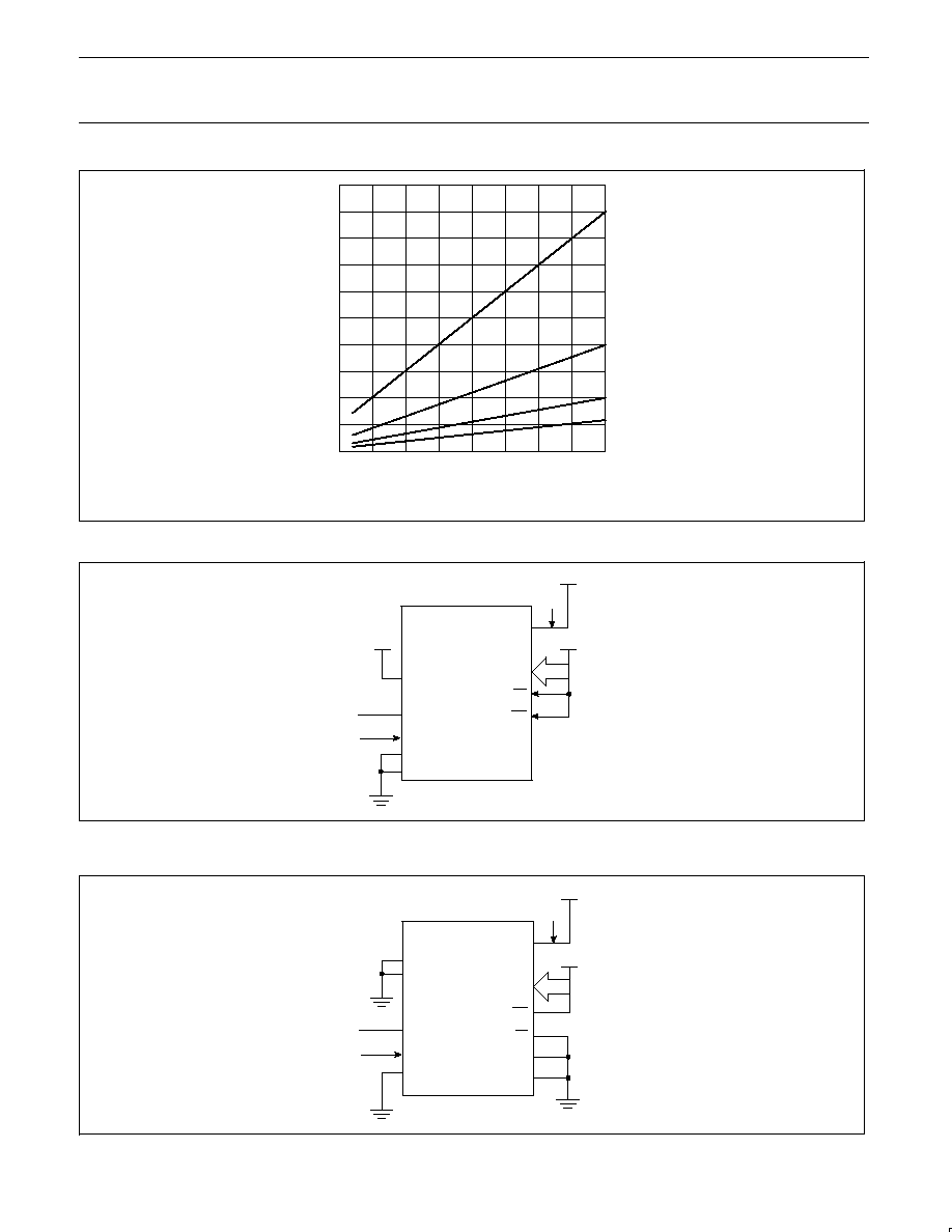
40
30
20
10
12
4
16
8
f (MHz)
(1)
NOTE:
These values are valid only within the frequency
specifications of the device under test.
IDD mA
50
0
0
(2)
(3)
(4)
(1) Maximum operating mode; VDD = 6V
(2) Maximum operating mode; VDD = 4V
(3) Maximum idle mode; VDD = 6V
(4) Maximum idle mode; VDD = 4V
SU00229
Figure 8. Supply Current (I
DD
) as a Function of Frequency at XTAL1 (f
OSC
)
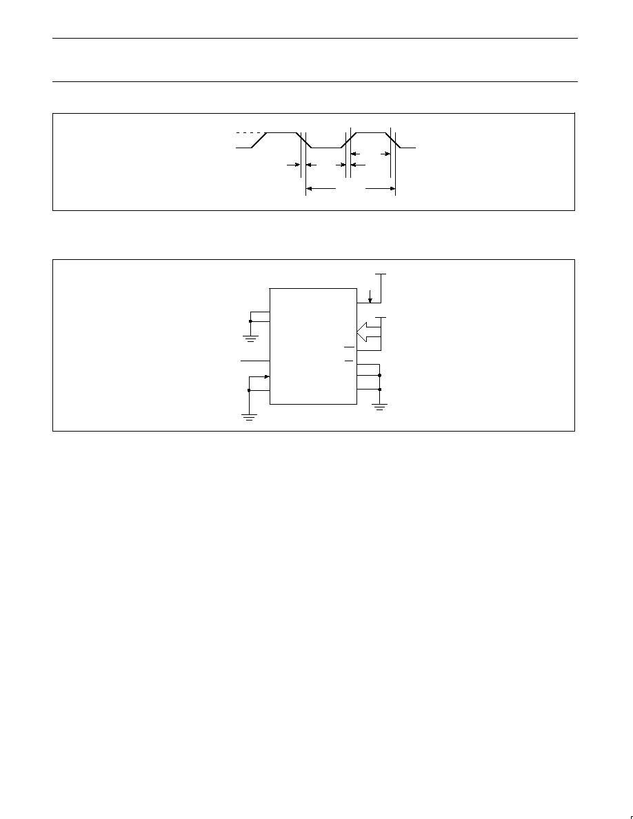
VDD
P0
EA
RST
XTAL1
XTAL2
VSS
VDD
VDD
VDD
IDD
(NC)
CLOCK SIGNAL
EW
STADC
SU00230
Figure 9. I
DD
Test Condition, Active Mode
All other pins are disconnected
VDD
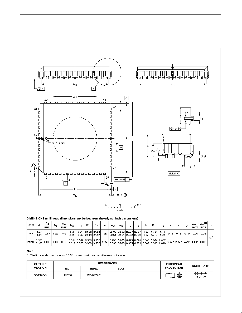
P0
EA
RST
XTAL1
XTAL2
VSS
VDD
VDD
IDD
(NC)
CLOCK SIGNAL
STADC
EW
AVSS
AVref
SU00231
Figure 10. I
DD
Test Condition, Idle Mode
All other pins are disconnected
Philips Semiconductors
Product specification
80C562/83C562
Single-chip 8-bit microcontroller
1992 Jan 08
14
VDD≠0.5
0.5V
t
CHCL
t
CLCL
t
CLCH
t
CLCX
t
CHCX
SU00232
Figure 11. Clock Signal Waveform for I
DD
Tests in Active and Idle Modes
t
CLCH
= t
CHCL
= 10ns
VDD
P0
EA
RST
XTAL1
XTAL2
VSS
VDD
VDD
IDD
(NC)
STADC
EW
AVSS
AVref
SU00233
Figure 12. I
DD
Test Condition, Power Down Mode
All other pins are disconnected. V
DD
= 2V to 5.5V
Philips Semiconductors
Product specification
80C562/83C562
Single-chip 8-bit microcontroller
1992 Jan 08
15
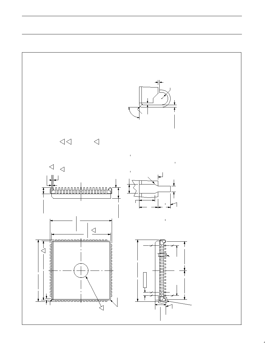
PLCC68:
plastic leaded chip carrier; 68 leads; pedestal
SOT188-3
Philips Semiconductors
Product specification
80C562/83C562
Single-chip 8-bit microcontroller
1992 Jan 08
16
1473A
68-PIN CERQUAD J-BEND (K) PACKAGE
NOTES:
1.
All dimensions and tolerances to conform
2.
UV window is optional.
3.
Dimensions do not include glass protrusion.
Glass protrusion to be 0.005 inches maximum
4.
Controlling dimension millimeters.
5.
All dimensions and tolerances include
lead trim of
fset and lead plating finish.
6.
Backside solder relief is optional and
dimensions are for reference only
.
1.02 (0.040) X 45
∞
24.51 (0.965)
23.62 (0.930)
25.27 (0.995)
25.02 (0.985)
CHAMFER
45
24.51 (0.965)
23.62 (0.930)
25.27 (0.995)
25.02 (0.985)
on each side.
to ANSI
Y14.5≠1982.
2
3
3
3 X 0.63 (0.025) R MIN.
3.05 (0.120)
2.29 (0.090)
4.83 (0.190)
3.94 (0.155)
SEA
TING
PLANE
0.38 (0.015)
0.51 (0.02) X 45
∞
6
6
25.27 (0.995)
25.02 (0.985)
1.27 (0.050)
20.32 (0.800) NOMINAL
1
1.94 (0.470)
1
1.18 (0.440)
1
1.94 (0.470)
1
1.18 (0.440)
64X
4.83 (0.190)
3.94 (0.155)
SEA
TING
PLANE
0.15 (0.006) MIN.
0.25 (0.010) R MIN.
0.508 (0.020) R MIN.
0.25 (0.010)
0.15 (0.006)
90
+ 5
≠10
∞∞
∞
0.076 (0.003) MIN.
DET
AIL
B
mm/(inch)
SEE DET
AIL
B
SEE DET
AIL
A
DET
AIL
A
TYP
. ALL
SIDES
mm/(inch)
1.52 (0.060) REF
.
0.482 (0.019 + 0.002)
SEA
TING
PLANE
1.02 + 0.25 (0.040 + 0.010)
BASE PLANE
45
TYP
.
4 PLACES
∞
0.73 + 0.08 (0.029 + 0.003)
1.27 (0.050)
TYP
.
853-1473A 05854

Philips Semiconductors
Product specification
80C562/83C562
Single-chip 8-bit microcontroller
1992 Jan 08
17
NOTES

Philips Semiconductors
Product specification
80C562/83C562
Single-chip 8-bit microcontroller
1992 Jan 08
18
NOTES

Philips Semiconductors
Product specification
80C562/83C562
Single-chip 8-bit microcontroller
1992 Jan 08
19
NOTES
Philips Semiconductors Microcontroller Products
Product specification
80C562/83C562
Single-chip 8-bit microcontroller
Philips Semiconductors and Philips Electronics North America Corporation reserve the right to make changes, without notice, in the products,
including circuits, standard cells, and/or software, described or contained herein in order to improve design and/or performance. Philips
Semiconductors assumes no responsibility or liability for the use of any of these products, conveys no license or title under any patent, copyright,
or mask work right to these products, and makes no representations or warranties that these products are free from patent, copyright, or mask
work right infringement, unless otherwise specified. Applications that are described herein for any of these products are for illustrative purposes
only. Philips Semiconductors makes no representation or warranty that such applications will be suitable for the specified use without further testing
or modification.
LIFE SUPPORT APPLICATIONS
Philips Semiconductors and Philips Electronics North America Corporation Products are not designed for use in life support appliances, devices,
or systems where malfunction of a Philips Semiconductors and Philips Electronics North America Corporation Product can reasonably be expected
to result in a personal injury. Philips Semiconductors and Philips Electronics North America Corporation customers using or selling Philips
Semiconductors and Philips Electronics North America Corporation Products for use in such applications do so at their own risk and agree to fully
indemnify Philips Semiconductors and Philips Electronics North America Corporation for any damages resulting from such improper use or sale.
This data sheet contains preliminary data, and supplementary data will be published at a later date. Philips
Semiconductors reserves the right to make changes at any time without notice in order to improve design
and supply the best possible product.
Philips Semiconductors
811 East Arques Avenue
P.O. Box 3409
Sunnyvale, California 94088≠3409
Telephone 800-234-7381
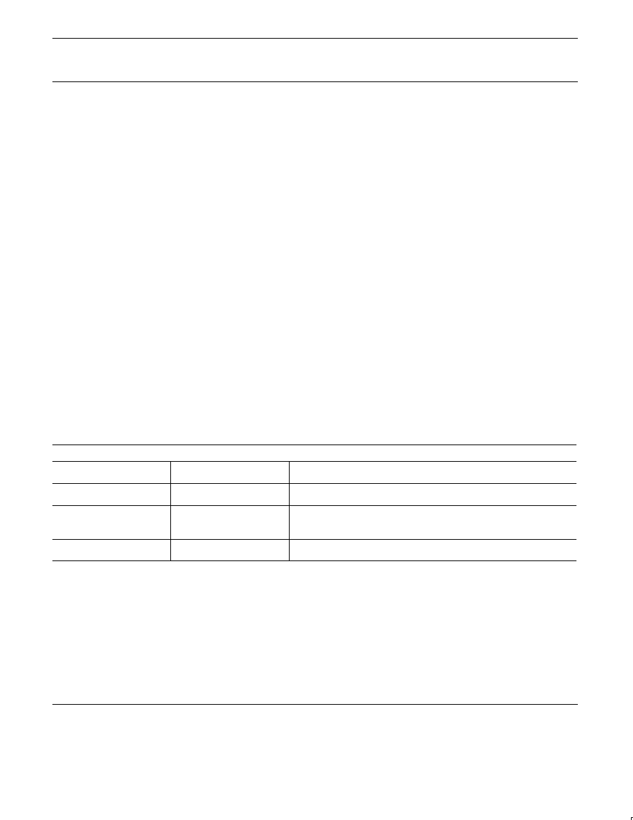
DEFINITIONS
Data Sheet Identification
Product Status
Definition
Objective Specification
Preliminary Specification
Product Specification
Formative or in Design
Preproduction Product
Full Production
This data sheet contains the design target or goal specifications for product development. Specifications
may change in any manner without notice.
This data sheet contains Final Specifications. Philips Semiconductors reserves the right to make changes
at any time without notice, in order to improve design and supply the best possible product.
Philips Semiconductors and Philips Electronics North America Corporation
register eligible circuits under the Semiconductor Chip Protection Act.
©
Copyright Philips Electronics North America Corporation 1992
All rights reserved. Printed in U.S.A.