 | –≠–ª–µ–∫—Ç—Ä–æ–Ω–Ω—ã–π –∫–æ–º–ø–æ–Ω–µ–Ω—Ç: 83C576 | –°–∫–∞—á–∞—Ç—å:  PDF PDF  ZIP ZIP |

Philips
Semiconductors
83C576/87C576
80C51 8-bit microcontroller family
8K/256 OTP/ROM, 6 channel 10-bit A/D,
4 comparators, failure detect circuitry, watchdog timer
Product specification
Supersedes data of 1998 Jan 06
IC20 Data Handbook
1998 Jun 04
INTEGRATED CIRCUITS

Philips Semiconductors
Product specification
83C576/87C576
80C51 8-bit microcontroller family
8K/256 OTP/ROM, 6 channel 10-bit A/D, 4 comparators,
failure detect circuitry, watchdog timer
2
1998 Jun 04
853-2067 19495
FEATURES
∑
80C51 based architecture
≠ 8k
◊
8 ROM (83C576)
≠ 8k
◊
8 EPROM (87C576)
≠ 256
◊
8 RAM
≠ 10-bit, 6 channel A/D
≠ Three 16-bit counter/timers
≠ 2 PWM outputs
≠ Programmable Counter Array
≠ Universal Peripheral Interface
≠ Enhanced UART
≠ Oscillator fail detect
≠ Low active reset
≠ 4 analog comparators
≠ Watchdog timer
≠ Low V
CC
detect
≠ Power-on detect
∑
Memory addressing capability
≠ 64k ROM and 64k RAM
∑
Power control modes:
≠ Idle mode
≠ Power-down mode
∑
CMOS and TTL compatible
∑
6 to 16MHz
∑
Extended temperature ranges
∑
OTP available
∑
That can be programmed in circuit
∑
Software Reset
∑
15 source, 2 level interrupt structure
∑
Lower EMI noise
∑
Programmable I/O pins
∑
Serial on-board programming
∑
Schmitt trigger inputs on Port 1
DESCRIPTION
The Philips 83C576/87C576 is a high-performance microcontroller
fabricated with Philips high-density CMOS technology. The Philips
CMOS technology combines the high speed and density
characteristics of HMOS with the low power attributes of CMOS.
Philips epitaxial substrate minimizes latch-up sensitivity.
The 8XC576 contains an 8k
◊
8 ROM (83C576) EPROM (87C576),
a 256
◊
8 RAM, 32 I/O lines, three 16-bit counter/timers, a
Programmable Counter Array (PCA), a 10-bit, 6 channel A/D,
2 PWM outputs, an 8-bit UPI interface, a fifteen-source, two-priority
level nested interrupt structure, an enhanced UART, four analog
comparators, power-fail detect and oscillator fail detect circuits, and
on-chip oscillator and clock circuits.
In addition, the 8XC576 has a low active reset, and a software reset.
There is also a fully configurable watchdog timer, and internal power
on clear circuit. The part includes idle mode and power-down mode
states for reduced power consumption.
ORDERING INFORMATION
ROM
EPROM
1
TEMPERATURE RANGE
∞
C AND PACKAGE
FREQ
(MHz)
DRAWING
NUMBER
P83C576EBP N
P87C576EBPN
OTP
0 to +70, 40-Pin Plastic Dual In-line Package
16
SOT129-1
P83C576EBA A
P87C576EBAA
OTP
0 to +70, 44-Pin Plastic Leaded Chip Carrier
16
SOT187-2
P83C576EBB B
P87C576EBBB
OTP
0 to +70, 44-Pin Plastic Quad Flat Pack
16
SOT307-2
P83C576EFP N
P87C576EBPN
OTP
≠40 to +85, 40-Pin Plastic Dual In-line Package
16
SOT129-1
P83C576EFA A
P87C576EFA A
OTP
≠40 to +85, 44-Pin Plastic Leaded Chip Carrier
16
SOT187-2
P83C576EFB B
P87C576EFB B
OTP
≠40 to +85, 44-Pin Plastic Quad Flat Pack
16
SOT307-2
P83C576EHPN
P87C576EHPN
OTP
≠40 to +125, 40-Pin Plastic Dual In-line Package
16
SOT129-1
P83C576EHAA
P87C576EHAA
OTP
≠40 to +125, 44-Pin Plastic Leaded Chip Carrier
16
SOT187-2
P83C576EHBB
P87C576EHBB
OTP
≠40 to +125, 44-Pin Plastic Quad Flat Pack
16
SOT307-2
NOTE:
1. OTP - One Time Programmable EPROM.

Philips Semiconductors
Product specification
83C576/87C576
80C51 8-bit microcontroller family
8K/256 OTP/ROM, 6 channel 10-bit A/D, 4 comparators,
failure detect circuitry, watchdog timer
1998 Jun 04
3
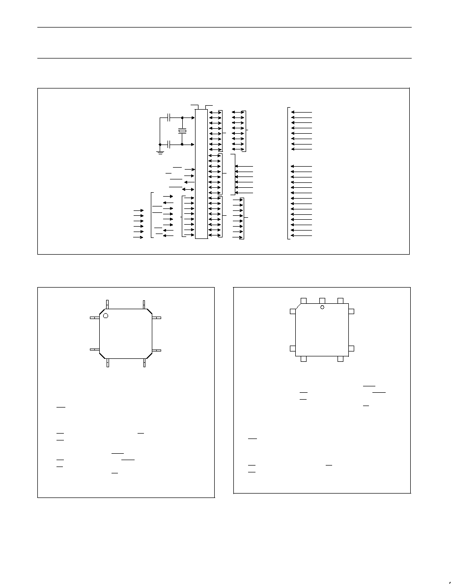
BLOCK DIAGRAM
PSEN
EA
ALE
RST
XTAL1
XTAL2
V
CC
V
SS
PORT 0
DRIVERS
PORT 2
DRIVERS
RAM ADDR
REGISTER
RAM
PORT 0
LATCH
PORT 2
LATCH
ROM/
EPROM
REGISTER
B
ACC
TMP2
TMP1
ALU
TIMING
AND
CONTROL
INSTRUCTION
REGISTER
PD
OSCILLATOR
PSW
PORT 1
LATCH
PORT 3
LATCH
PORT 1
DRIVERS
PORT 3
DRIVERS
PROGRAM
ADDRESS
REGISTER
BUFFER
PC
INCRE-
MENTER
PROGRAM
COUNTER
DPTR
P1.0-P1.5
P3.0-P3.7
P0.0-P0.7
P2.0-P2.7
STACK
POINTER
SFRs
TIMERS
PCA
10-BIT
ANALOG TO DIGITAL
CONVERTER
SU00255B
UPI
CONTROL
LOW
VOLTAGE
DETECT
POWER
ON
DETECT
A
B
WATCHDOG
TIMER
A
B
CLK AND OSC
FAILURE
DETECT
COMPARATOR
BLOCK
PWM
≠AV
SS
+AV
CC
Philips Semiconductors
Product specification
83C576/87C576
80C51 8-bit microcontroller family
8K/256 OTP/ROM, 6 channel 10-bit A/D, 4 comparators,
failure detect circuitry, watchdog timer
1998 Jun 04
4
LOGIC SYMBOL
POR
T
0
POR
T
1
POR
T
2
POR
T
3
ADDRESS AND
DATA BUS
ADDRESS BUS
RxD
TxD
INT0
INT1
T0
T1
WR
RD
SECONDAR
Y
FUNCTIONS
RST
EA/VPP
PSEN
ALE/PROG
VSS
VCC
XTAL1
XTAL2
CMP1+
CMPR≠
CMP0+
CMP0≠
CMP3+
CMP2+
SECONDAR
Y
FUNCTIONS
DB0
DB1
DB2
DB3
DB4
DB5
DB6
DB7
ADIN0
ADIN1
ADIN2
ADIN3
ADIN4
ADIN5
PWM1/ECI
CEX4/PWM0
T2/CS#
T2EX/A0
CEX3/CMP3
CEX2/CMP2
CEX1/CMP1
CEX0/CMP0
SU00254A
PIN CONFIGURATIONS
44-pin Plastic Quad Flat Pack
Pin Function
1
ADIN3/P1.3
2
ADIN4/P1.4
3
ADIN5/P1.5
4
RST
5
RxD/P3.0
6
NC*
7
TXD/P3.1
8
INT0/P3.2/CMP3+
9
INT1/P3.3/CMP2+
10
T0/P3.4/CMP1+
11
T1/P3.5/CMPR≠
12
WR/P3.6/CMP0+
13
RD/P3.7CMP0≠
14
XTAL2
15
XTAL1
SU00253B
Pin Function
31
P0.6/AD6/DB6
32
P0.5/AD5/DB5
33
P0.4/AD4/DB4
34
P0.3/AD3/DB3
35
P0.2/AD2/DB2
36
P0.1/AD1/DB1
37
P0.0/AD0/DB0
38
V
CC
39
NC*
40
+V
REF
/AV
CC
41
≠V
REF
/AV
SS
42
ADIN0/P1.0
43
ADIN1/P1.1
44
ADIN2/P1.2
PQFP
44
34
1
11
33
23
12
22
Pin Function
16
V
SS
17
NC*
18
P2.0/A8/CEX0/CMP0
19
P2.1/A9/CEX1/CMP1
20
P2.2/A10/CEX2/CMP2
21
P2.3/A11/CEX3/CMP3
22
P2.4/A12/T2EX/A0
23
P2.5/A13/T2/CS
24
P2.6/A14/CEX4/PWM0
25
P2.7/A15/PWM1/ECI
26
PSEN
27
ALE/PROG
28
NC*
29
EA/V
PP
30
P0.7/AD7/DB7
* NO INTERNAL CONNECTION
Plastic Leaded Chip Carrier
LCC
6
1
40
7
17
39
29
18
28
Pin Function
31
P2.7/A15/PWM1/ECI
32
PSEN
33
ALE/PROG
34
NC*
35
EA/V
PP
36
P0.7/AD7/DB7
37
P0.6/AD6/DB6
38
P0.5/AD5/DB5
39
P0.4/AD4/DB4
40
P0.3/AD3/DB3
41
P0.2/AD2/DB2
42
P0.1/AD1/DB1
43
P0.0/AD0/DB0
44
V
CC
SU00252A
Pin Function
16
T0/P3.4/CMP1+
17
T1/P3.5/CMPR≠
18
WR/P3.6/CMP0+
19
RD/P3.7/CMP0≠
20
XTAL2
21
XTAL1
22
V
SS
23
NC*
24
P2.0/A8/CEX0/CMP0
25
P2.1/A9/CEX1/CMP1
26
P2.2/A10/CEX2/CMP2
27
P2.3/A11/CEX3/CMP3
28
P2.4/A12/T2EX/A0
29
P2.5/A13/T2/CS
30
P2.6/A14/CEX4/PWM0
Pin Function
1
NC*
2
+V
REF
/AV
CC
3
≠V
REF
/AV
SS
4
ADIN0/P1.0
5
ADIN1/P1.1
6
ADIN2/P1.2
7
ADIN3/P1.3
8
ADIN4/P1.4
9
ADIN5/P1.5
10
RST
11
RxD/P3.0
12
NC*
13
TxD/P3.1
14
INT0/P3.2/CMP3+
15
INT1/P3.3/CMP2+
* NO INTERNAL CONNECTION

Philips Semiconductors
Product specification
83C576/87C576
80C51 8-bit microcontroller family
8K/256 OTP/ROM, 6 channel 10-bit A/D, 4 comparators,
failure detect circuitry, watchdog timer
1998 Jun 04
5
PIN DESCRIPTIONS
PIN NUMBER
MNEMONIC
DIP
LCC
QFP
TYPE
NAME AND FUNCTION
V
SS
20
22
16
I
Ground: 0V reference.
V
CC
40
44
38
I
Power Supply: This is the power supply voltage for normal, idle, and power-down operation.
P0.0-0.7
39-32
43-36
37-30
I/O
Port 0: Port 0 is a bidirectional I/O port. Port 0 is also the multiplexed low-order address and
data bus during accesses to external program and data memory (see Note 5). In this
application, it uses strong internal pull-ups when emitting 1s. Port 0 also receives code bytes
during parallel EPROM programming and outputs code bytes during verification. External
pull-ups are required during program verification. During reset, the port register is loaded
with 1's. Port 0 has 4 output modes selected on a per bit basis by writing to the P0M1 and
P0M2 Special Function Registers as follows:
P0M1.x
P0M2.x
Mode Description
0
0
Open drain (default). See Note 1.
0
1
Weak pullup. See Note 2.
1
0
High impedance. See Note 3.
1
1
Push-pull. See Note 4.
Port 0 is also the data I/O port for the Universal Peripheral Interface (UPI). When the UPI is
enabled, port 0 must be configured as High-Z by the user. Input/Output through P0 is
controlled by pin CS, WR, RD, and A0. Output is push-pull when enabled.
P1.0-P1.5
3-8
5-9
42-44
1-3
I/O
Port 1: Port 1 is a 6-bit bidirectional I/O port with Schmitt trigger inputs. Port 1 receives the control
signals during program memory verification and parallel EPROM programming. During reset, port
1 is configured as a high impedance analog input port. Digital push-pull outputs are enabled by
writing 1's to the P1M1 register. The programmer must take care to prevent digital outputs from
switching while an A/D conversion is in progress. Port 1 has 3 output modes selected on a per bit
basis by writing to the P1M1 and P1M2 special function registers as follows:
P1M1.X
P1M2.X
Mode Description
0
0
A/D only. (High impedance)
0
1
Digital input only. High impedance (default).
1
X
Push-pull.
Port 1 pins also serve alternate functions as follows:
3
4
42
I/O
P1.0/ADIN0
4
5
43
I/O
P1.1/ADIN1
5
6
44
I/O
P1.2/ADIN2
6
7
1
I/O
P1.3/ADIN3
7
8
2
I/O
P1.4/ADIN4
8
9
3
I/O
P1.5/ADIN5
P2.0-P2.7
21-28
24-31
18-25
I/O
Port 2: Port 2 is an 8-bit bidirectional I/O port. Port 2 emits the high-order address byte
during accesses to external program and data memory that use 16-bit addresses (MOVX
@DPTR) (see Note 5). In this application, it uses strong internal pull-ups when emitting 1s.
Port 2 receives the high-order address byte during program verification and parallel EPROM
programming. During reset, the port 2 pullups are turned on synchronously, and the port
register is loaded with 1's. Port 2 has the following output modes which can be selected on a
per bit basis by writing to P2M1 and P2M0:
P2M1.X
P2M2.X
Mode Description
0
0
Open drain. See Note 1.
0
1
Weak pullup (default). See Note 2.
1
0
High impedance. See Note 3.
1
1
Push-pull. See Note 4.
Port 2 pins serve alternate functions as follows:
21
24
18
P2.0
CEX0
PCA module 0 external I/O
CMP0
comparator 0 output
22
25
19
P2.1
CEX1
PCA module 1 external I/O
CMP1
comparator 1 output
23
26
20
P2.2
CEX2
PCA module 2 external I/O
CMP2
comparator 2 output
24
27
21
P2.3
CEX3
PCA module 3 external I/O
CMP3
comparator 3 output
25
28
22
P2.4
T2EX
timer 2 capture input
A0
UPI address input
26
29
23
P2.5
T2
timer 2 external I/O -- clock-out (programmable)
CS
UPI chip select input
27
30
24
P2.6
CEX4
PCA module 4 external I/O
PWM0
Pulse width modulator 0 output
28
31
25
P2.7
ECI
PCA count input
PWM1
Pulse width modulator 1 output