Philips Semiconductors
Preliminary specification
83C749/87C749
80C51 8-bit microcontroller family
2K/64 OTP/ROM, 5 channel 8-bit A/D, PWM, low pin count
2
1998 Apr 23
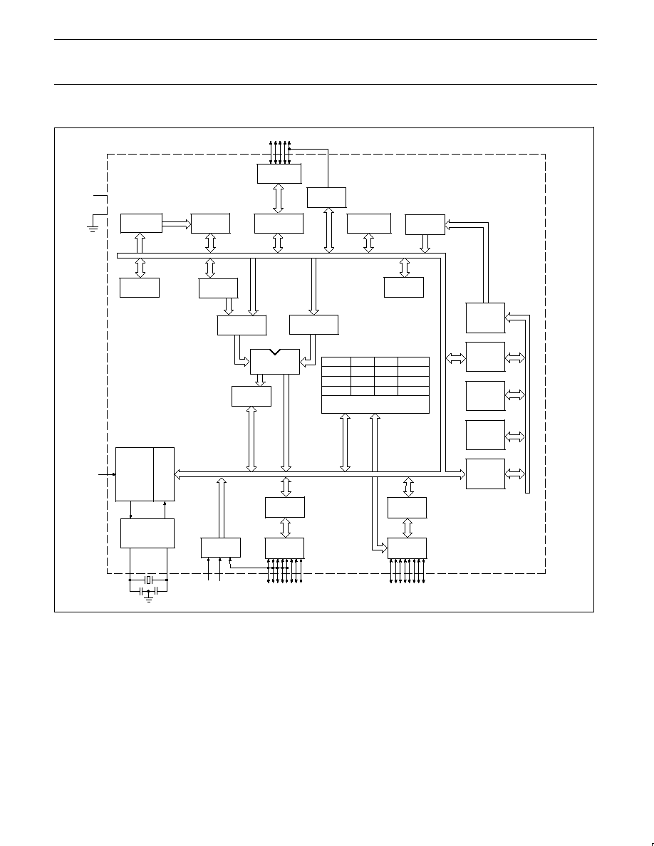
DESCRIPTION
The Philips 83C749/87C749 offers many of the advantages of the
80C51 architecture in a small package and at low cost.
The 8XC749 Microcontroller is fabricated with Philips high-density
CMOS technology. Philips epitaxial substrate minimizes CMOS
latch-up sensitivity.
The 8XC749 contains a 2k
◊
8 ROM (83C749) EPROM (87C749), a
64
◊
8 RAM, 21 I/O lines, a 16-bit auto-reload counter/timer, a
fixed-priority level interrupt structure, an on-chip oscillator, a five
channel multiplexed 8-bit A/D converter, and an 8-bit PWM output.
The EPROM version of this device, the 87C749, is available in
plastic one-time programmable (OTP) packages. Once the array
has been programmed, it is functionally equivalent to the masked
ROM 83C749. Thus, unless explicitly stated otherwise, all
references made to the 83C749 apply equally to the 87C749.
The 83C749 supports two power reduction modes of operation
referred to as the idle mode and the power-down mode.
FEATURES
∑
Available in erasable quartz lid or One-Time Programmable plastic
packages
∑
80C51 based architecture
∑
Small package sizes
≠ 28-pin DIP
≠ 28-pin Shrink Small Outline Package (SSOP)
≠ 28-pin PLCC
∑
Wide oscillator frequency range:
3.5MHz to 16MHz
∑
Low power consumption:
≠ Normal operation: less than 11mA @ 5V, 12MHz
≠ Idle mode
≠ Power-down mode
∑
2k
◊
8 ROM (83C749)
EPROM (87C749)
∑
64
◊
8 RAM
∑
16-bit auto reloadable counter/timer
∑
5-channel 8-bit A/D converter
∑
8-bit PWM output/timer
∑
10-bit fixed-rate timer
∑
Boolean processor
∑
CMOS and TTL compatible
∑
Well suited for logic replacement, consumer and industrial
applications
PART NUMBER SELECTION
ROM
EPROM
1
TEMPERATURE RANGE
∞
C
AND PACKAGE
FREQUENCY
DRAWING
NUMBER
P83C749EBP N
P87C749EBP N
OTP
0 to +70, 28-pin Plastic Dual In-line Package
3.5 to 16MHz
SOT117-2
P83C749EBA A
P87C749EBA A
OTP
0 to +70, 28-pin Plastic Leaded Chip Carrier
3.5 to 16MHz
SOT261-3
P83C749EBD DB
P87C749EBD DB
OTP
0 to +70, 28-pin Shrink Small Outline Package
3.5 to 16MHz
SOT341-1
NOTE:
1. OTP = One Time Programmable EPROM.

Philips Semiconductors
Preliminary specification
83C749/87C749
80C51 8-bit microcontroller family
2K/64 OTP/ROM, 5 channel 8-bit A/D, PWM, low pin count
1998 Apr 23
5
PIN DESCRIPTION
MNEMONIC
PIN NO.
TYPE
NAME AND FUNCTION
V
SS
12
I
Circuit Ground Potential.
V
CC
28
I
Supply voltage during normal, idle, and power-down operation.
P0.0≠P0.4
8≠6
23, 24
I/O
Port 0: Port 0 is a 5-bit bidirectional port. Port 0.0≠P0.2 are open drain. Port 0.0≠P0.2 pins that have
1s written to them float, and in that state can be used as high-impedance inputs. P0.3≠P0.4 are
bidirectional I/O port pins with internal pull-ups. These pins are driven low if the port register bit is
written with a 0. The state of the pin can always be read from the port register by the program. Port 0.3
and 0.4 have internal pull-ups that function identically to port 3. Pins that have 1s written to them are
pulled high by the internal pull-ups and can be used as inputs.
While P0.0 anbd P0.1 differ from "standard TTL" characteristics, they are close enough for the pins to
still be used as general-purpose I/O.
6
I
V
PP
(P0.2) ≠ Programming voltage input. (See Note 2.)
7
I
OE/PGM (P0.1) ≠ Input which specifies verify mode (output enable) or the program mode.
OE/PGM = 1 output enabled (verify mode).
OE/PGM = 0 program mode.
8
I
ASEL (P0.0) ≠ Input which indicates which bits of the EPROM address are applied to port 3.
ASEL = 0 low address byte available on port 3.
ASEL = 1 high address byte available on port 3 (only the three least significant bits are used).
P1.0≠P1.7
13≠17,
20≠22
I/O
Port 1: Port 1 is an 8-bit bidirectional I/O port with internal pull-ups. Port 1 pins that have 1s written to
them are pulled high by the internal pull-ups and can be used as inputs. P0.3≠P0.4 pins are
bidirectional I/O port pins with internal pull-ups. As inputs, port 1 pins that are externally pulled low will
source current because of the internal pull-ups. (See DC Electrical Characteristics: I
IL
). Port 1 also
serves the special function features of the SC80C51 family as listed below:
20
I
INT0 (P1.5): External interrupt.
21
I
INT1 (P1.6): External interrupt.
22
I
T0 (P1.7): Timer 0 external input.
13≠17
I
ADC0 (P1.0)≠ADC4 (P1.4): Port 1 also functions as the inputs to the five channel multiplexed A/D
converter. These pins can be used as outputs only if the A/D function has been disabled. These pins
can be used as digital inputs while the A/D converter is enabled.
Port 1 serves to output the addressed EPROM contents in the verify mode and accepts as inputs the
value to program into the selected address during the program mode.
P3.0≠P3.7
5≠1,
27≠25
I/O
Port 3: Port 3 is an 8-bit bidirectional I/O port with internal pull-ups. Port 3 pins that have 1s written to
them are pulled high by the internal pull-ups and can be used as inputs. As inputs, port 3 pins that are
externally being pulled low will source current because of the pull-ups. (See DC Electrical
Characteristics: I
IL
). Port 3 also functions as the address input for the EPROM memory location to be
programmed (or verified). The 11-bit address is multiplexed into this port as specified by P0.0/ASEL.
RST
9
I
Reset: A high on this pin for two machine cycles while the oscillator is running resets the device. An
internal diffused resistor to V
SS
permits a power-on RESET using only an external capacitor to V
CC
.
After the device is reset, a 10-bit serial sequence, sent LSB first, applied to RESET, places the device
in the programming state allowing programming address, data and V
PP
to be applied for programming
or verification purposes. The RESET serial sequence must be synchronized with the X1 input.
X1
11
I
Crystal 1: Input to the inverting oscillator amplifier and input to the internal clock generator circuits. X1
also serves as the clock to strobe in a serial bit stream into RESET to place the device in the
programming state.
X2
10
O
Crystal 2: Output from the inverting oscillator amplifier.
AV
CC
1
19
I
Analog supply voltage and reference input.
AV
SS
1
18
I
Analog supply and reference ground.
NOTE:
1. AV
SS
(reference ground) must be connected to 0V (ground). AV
CC
(reference input) cannot differ from V
CC
by more than
±
0.2V, and must be
in the range 4.5V to 5.5V.
2. When P0.2 is at or close to 0 volt, it may affect the internal ROM operation. We recommend that P0.2 be tied to V
CC
via a small pullup
(e.g., 2k
).