 | –≠–ª–µ–∫—Ç—Ä–æ–Ω–Ω—ã–π –∫–æ–º–ø–æ–Ω–µ–Ω—Ç: 84C444 | –°–∫–∞—á–∞—Ç—å:  PDF PDF  ZIP ZIP |

DATA SHEET
Product specification
Supersedes data of October 1994
File under Integrated Circuits, IC14
1996 Nov 29
INTEGRATED CIRCUITS
84C44X; 84C64X; 84C84X
8-bit microcontrollers with
OSD and VST

1996 Nov 29
2
Philips Semiconductors
Product specification
8-bit microcontrollers with OSD and VST
84C44X; 84C64X; 84C84X
CONTENTS
1
FEATURES
1.1
PCF84CXXXA kernel
1.2
Derivative features PCA84C640
2
GENERAL DESCRIPTION
2.1
Important note
3
ORDERING INFORMATION
4
BLOCK DIAGRAM
5
PINNING INFORMATION
6
DIFFERENCES BETWEEN THE TYPES
7
RESET
7.1
Power-on-reset
8
ANALOG CONTROL
8.1
6-bit PWM DACs
9
VST CONTROL
9.1
14-bit PWM DAC
9.2
Coarse adjustment
9.3
Fine adjustment
10
AFC INPUT
11
INPUT/OUTPUT (I/O)
12
ON SCREEN DISPLAY
12.1
Features
12.2
Horizontal display position control
12.3
Vertical display position control
12.4
Clock generator
12.5
Display data registers
12.6
Display control registers
12.7
OSD display position
12.8
OSD character size and colour selection
12.9
Character ROM
13
EMULATION MODE
14
REGISTER MAP
15
LIMITING VALUES
16
DC CHARACTERISTICS
17
AC CHARACTERISTICS
17.1
Characteristic curves
18
PACKAGE OUTLINE
19
SOLDERING
19.1
Introduction
19.2
Soldering by dipping or by wave
19.3
Repairing soldered joints
20
DEFINITIONS
21
LIFE SUPPORT APPLICATIONS
22
PURCHASE OF PHILIPS I
2
C COMPONENTS

1996 Nov 29
3
Philips Semiconductors
Product specification
8-bit microcontrollers with OSD and VST
84C44X; 84C64X; 84C84X
1
FEATURES
1.1
PCF84CXXXA kernel
∑
8-bit CPU, ROM, RAM, I/O in a single 42 leads shrink
DIL package
∑
Over 80 instructions all of 1 or 2 cycles
∑
29 quasi-bidirectional standard I/O port lines
∑
Configuration of I/O lines individually selected by mask
∑
External interrupt INT/T0
∑
2 direct testable inputs T0 and T1
∑
8-bit programmable timer/event counter
∑
3 single level vectored interrupts (external,
timer/counter, I
2
C-bus)
∑
Power-on-reset and low voltage detector
∑
Single power supply
∑
2 power reduction modes: Idle and Stop
∑
Operating temperature range:
-
20 to +70
∞
C
∑
Silicon gate CMOS fabrication process (SAC2).
1.2
Derivative features PCA84C640
Although the PCA84C640 is specifically referred to
throughout this data sheet, the information applies to all
the devices. The small differences between the 84C640
and the other devices are specified in the text and also
highlighted in Chapter 6.
The PCA84C640 comprises:
∑
The PCF84CXXXA processor core
∑
6 kbytes mask-programmable program ROM
∑
128 bytes RAM
∑
Multi-master I
2
C-bus interface
∑
AFC input for Voltage Synthesized Tuning
(VST; with 3-bit DAC and comparator)
∑
On Screen Display (OSD) facility for two rows of
16-characters
∑
On Screen Display character set of 64 types
∑
Four programmable display dot sizes
∑
Half dot character rounding
∑
Seven colours for each character
∑
One 14-bit PWM output for VST
∑
Five 6-bit PWM outputs for analog controls
∑
Eight port lines with 10 mA LED drive capability
∑
18 general purpose bidirectional I/O lines
plus 11 function-combined I/O lines
∑
2 direct testable lines
∑
Programmable VSYNCN and HSYNCN input polarity
∑
RC oscillator for OSD function.
2
GENERAL DESCRIPTION
The 84C44X; 84C64X; 84C84X denotes the types:
∑
PCA84C440; 84C441; 84C443; 84C444
∑
PCA84C640; 84C641; 84C643; 84C644
∑
PCA84C840; 84C841; 84C843; 84C844.
which are 8-bit microcontrollers with On Screen Display
(OSD) and Voltage Synthesized Tuning (VST) functions.
All are members of the 84CXXX microcontroller family.
There are two oscillator types for the OSD function in the
various types, i.e.,
∑
RC oscillator: PCA84C440; 84C443; 84C640; 84C643;
84C840; 84C843
∑
LC oscillator: PCA84C441; 84C444; 84C641; 84C644;
84C841; 84C844.
2.1
Important note
This data sheet details the specific properties of the
PCA84C44X, PCA84C64X and PCA84C84X.
The shared characteristics of the PCA84CXXX family of
microcontrollers are described in the PCF84CXXXA
Family single-chip 8-bit Microcontroller of
"Data Handbook
IC14", which should be read in conjunction with this data
sheet.
3
ORDERING INFORMATION
TYPE NUMBER
PACKAGE
TEMPERATURE
RANGE (
∞
C)
NAME
DESCRIPTION
VERSION
PCA84C440; 84C443; 84C640; 84C643;
84C840; 84C843
SDIP42
plastic shrink dual in-line
package; 42 leads (600 mil)
SOT270-1
-
20 to +70
PCA84C441; 84C444; 84C641; 84C644;
84C841; 84C844
1996 Nov 29
4
Philips Semiconductors
Product specification
8-bit microcontrollers with OSD and VST
84C44X; 84C64X; 84C84X
4
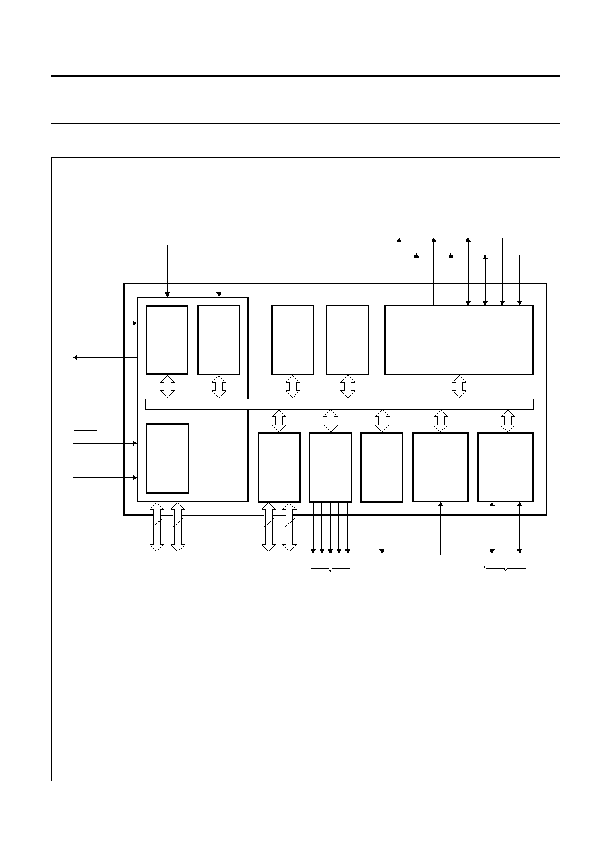
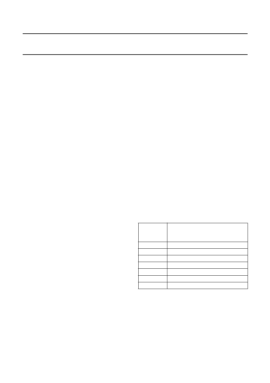
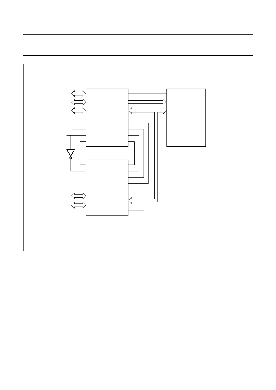
BLOCK DIAGRAM
Fig.1 Block diagram.
handbook, full pagewidth
84CXXX
core
excluding
ROM/RAM
8-bit internal bus
8-BIT
TIMER /
EVENT
COUNTER
CPU
PARALLEL
I/O
PORTS
ROM
(1)
RAM
(2)
8-BIT
I/O
PORTS
6-BIT
DAC
14-BIT
DAC
3-BIT DAC +
COMPARATOR
I C
INTERFACE
2
ON SCREEN DISPLAY
5
P0
P1
DP0
DP1
1 2 3 4 5
VOB
VOW1
VOW2
VOW3
DOSC1
DOSC2
(3)
VSYNCN
HSYNCN
TEST/EMU
XTAL1 (IN)
XTAL2 (OUT)
RESET
TDAC
AFC
SDA
SCL
MCD170
T1
INT/T0
PWM
(4)
(5)
(6)
8
8
8
(1) 4 kbytes for the PCA84C440; 84C441; 84C443; 84C444.
6 kbytes for the PCA84C640; 84C641; 84C643; 84C644.
8 kbytes for the PCA84C840; 84C841; 84C843; 84C844.
(2) 128 bytes for the PCA84C440; 84C441; 84C443; 84C444; 84C640; 84C641; 84C643; 84C644.
192 bytes for the PCA84C840; 84C841; 84C843; 84C844.
(3) For use with an LC oscillator, only available with the:
PCA84C441; 84C444; 84C641; 84C644; 84C841; 84C844.
(4) I
2
C-bus interface not available with the:
PCA84C443; 84C444; 84C643; 84C644; 84C843; 84C844.
(5) DP1.4 only available for PCA84C440; 84C443; 84C640; 84C643; 84C840; 84C843.
(6) T1 = pin 29 for PCA84C440; 84C443; 84C640; 84C643; 84C840; 84C843.
T1 = pin 34 for PCA84C441; 84C444; 84C641; 84C644; 84C841; 84C844.
1996 Nov 29
5
Philips Semiconductors
Product specification
8-bit microcontrollers with OSD and VST
84C44X; 84C64X; 84C84X
5
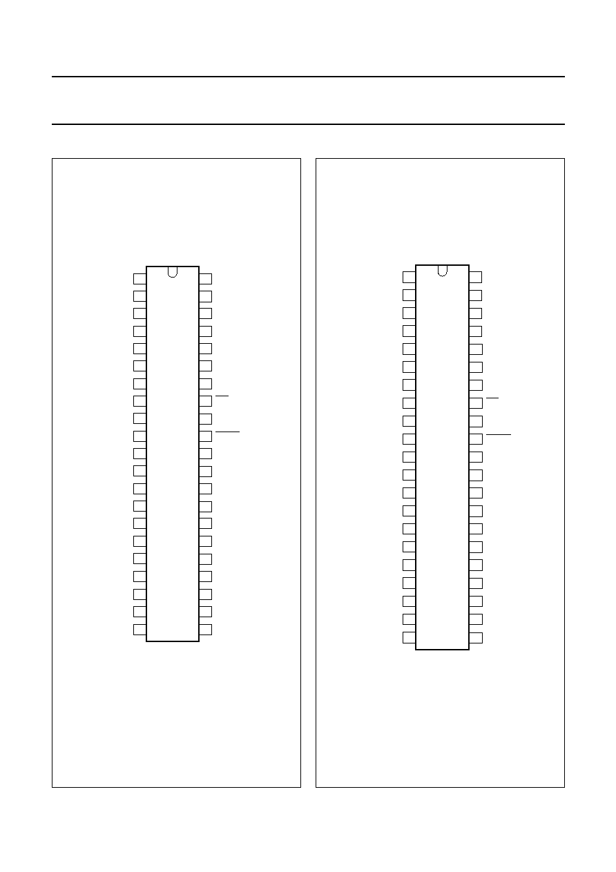
PINNING INFORMATION
Fig.2 Pinning diagram for PCA84CX40; 84CX43.
handbook, halfpage
MCD172
1
2
3
4
5
6
7
8
9
10
11
12
13
40
39
38
37
36
35
34
33
32
31
30
29
28
27
14
15
16
17
18
19
20
22
23
24
25
26
21
42
41
DP0.5/PWM5
DP0.4/PWM4
DP0.3/PWM3
DP0.2/PWM2
DP0.1/PWM1
DP0.0/TDAC
DP1.7/AFC
P1.0
P1.1
P1.2
P1.3
P1.4
P0.0
P0.1
P0.2
P0.3
P0.4
P0.5
P0.6
P0.7
V
SS
DP1.0
DP0.6/SDA
DP0.7/SCL
DP1.1
DP1.2
DP1.3
INT/T0
DP1.4
XTAL2
XTAL1
TEST/EMU
DOSC1
HSYNCN
VOW2/DP1.5
T1
VSYNCN
VOB
VOW1/DP1.6
VOW3
DD
V
RESET
PCA84C640
PCA84C643
PCA84C840
PCA84C843
PCA84C440
PCA84C443
handbook, halfpage
MCD171
1
2
3
4
5
6
7
8
9
10
11
12
13
40
39
38
37
36
35
34
33
32
31
30
29
28
27
14
15
16
17
18
19
20
22
23
24
25
26
21
42
41
DP0.5/PWM5
DP0.4/PWM4
DP0.3/PWM3
DP0.2/PWM2
DP0.1/PWM1
DP0.0/TDAC
DP1.7/AFC
P1.0
P1.1
P1.2
P1.3
P1.4
P0.0
P0.1
P0.2
P0.3
P0.4
P0.5
P0.6
P0.7
V
SS
PCA84C441
PCA84C444
PCA84C641
PCA84C644
PCA84C841
PCA84C844
DP1.0
DP0.6/SDA
DP0.7/SCL
DP1.1
DP1.2
DP1.3
INT/T0
T1
XTAL2
XTAL1
TEST/EMU
DOSC1
HSYNCN
VOW2/DP1.5
DOSC2
VSYNCN
VOB
VOW1/DP1.6
VOW3
DD
V
RESET
Fig.3 Pinning diagram for PCA84CX41; 84CX44.
1996
Nov
29
6
Philips Semiconductors
Product specification
8-bit microcontrollers with OSD and VST
84C44X; 84C64X; 84C84X
Table 1
Pin description
Note
1. 84CX40; 84CX43 denotes the types: PCA84C440, PCA84C443, PCA84C640, PCA84C643, PCA84C840 and PCA84C843.
84CX41; 84CX44 denotes the types: PCA84C441, PCA84C444, PCA84C641, PCA84C644, PCA84C841 and PCA84C844.
SYMBOL
(1)
PIN
(1)
DESCRIPTION
84CX40; 84CX43 84CX41; 84CX44 84CX40; 84CX43 84CX41; 84CX44
Deviating pinning
DP1.0 to DP1.4
DP1.0 to DP1.3
41, 38, 37, 36, 34 41, 38, 37, 36
Derivative Port 1: quasi-bidirectional I/O lines.
T1
T1
29
34
Direct testable pin and event counter input.
DOSC1
-
28
-
Connection to RC oscillator of OSD clock.
-
DOSC1/DOSC2
-
28, 29
Connections to LC oscillator of OSD clock.
Mutual pinning
DP0.0/TDAC
1
Derivative Port 0: quasi-bidirectional I/O line or 14-bit DAC PWM.
DP0.1 to DP0.5/PWM1 to PWM5
2 to 6
Derivative Port 1: quasi-bidirectional I/O lines or 6-bit DAC PWM.
P1.0 to P1.4
7, 8, 10, 11 and 12
Port 1: quasi-bidirectional I/O lines.
P0.0 to P0.7
13 to 20
Port 0: quasi-bidirectional I/O port.
DP1.7/AFC
9
Derivative Port 1:
quasi-bidirectional I/O line or comparator input with 3-bit DAC.
DP0.6/SDA
40
Derivative open drain I/O port or I
2
C-bus data line.
DP0.7/SCL
39
Derivative open drain I/O port or I
2
C- bus clock line.
INT/T0
35
External interrupt or direct testable line.
DP1.5 and DP1.6/VOW2 and VOW1
23, 22
Derivative Port 1:
quasi-bidirectional I/O lines or character video output.
RESET
33
Initialize input, active LOW.
XTAL2, XTAL1
32, 31
Oscillator output or input terminal for system clock.
TEST/EMU
30
Control input for testing and emulation mode. Ground for normal
operation.
VSYNCN
27
Vertical synchronous signal input.
HSYNCN
26
Horizontal synchronous signal input.
VOB
25
Blanking output.
VOW3
24
Character video output of OSD.
V
SS
21
Ground.
V
DD
42
Power supply.
1996
Nov
29
7
Philips Semiconductors
Product specification
8-bit microcontrollers with OSD and VST
84C44X; 84C64X; 84C84X
6
DIFFERENCES BETWEEN THE TYPES
Table 2
Differences between the types PCA84C44X, PCA84C64X and PCA84C84X
In this table: yes = available; no = not available.
FEATURE
PCA...
84C440 84C441 84C443 84C444 84C640 84C641 84C643 84C644 84C840 84C841 84C843 84C844
OSD oscillator
RC
LC
RC
LC
RC
LC
RC
LC
RC
LC
RC
LC
General purpose I/O lines 18
17
18
17
18
17
18
17
18
17
18
17
I
2
C-bus interface
yes
yes
no
no
yes
yes
no
no
yes
yes
no
no
ROM
4 kbytes
6 kbytes
8 kbytes
RAM
128 bytes
128 bytes
192 bytes
Pin assignment
Pin 29
T1
DOSC2 T1
DOSC2 T1
DOSC2 T1
DOSC2 T1
DOSC2 T1
DOSC2
Pin 34
DP1.4
T1
DP1.4
T1
DP1.4
T1
DP1.4
T1
DP1.4
T1
DP1.4
T1
Register DP1 (bit DP1.4)
Pin
yes
no
yes
no
yes
no
yes
no
yes
no
yes
no
Latch
yes
no
yes
no
yes
no
yes
no
yes
no
yes
no
1996 Nov 29
8
Philips Semiconductors
Product specification
8-bit microcontrollers with OSD and VST
84C44X; 84C64X; 84C84X
7
RESET
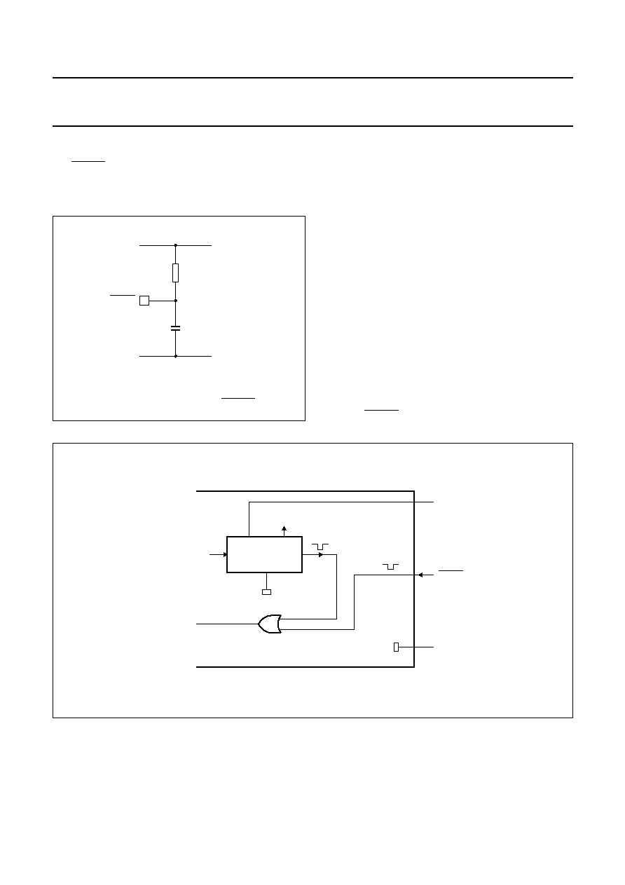
The RESET pin (active LOW input) is used to initialize the
microcontroller to a defined state. The Reset configuration
is shown in Fig.5.
Fig.4 External components for RESET pin.
andbook, halfpage
VSS
DD
V
R
100 k
C
RESET
MCD174
7.1
Power-on-reset
The Power-on-reset circuit monitors the voltage level of
V
DD
. If V
DD
remains below the internal reference voltage
level V
ref
(typically 1.3 V), the oscillator is inhibited.
When V
DD
rises above V
ref
, the oscillator is released and
the internal reset is active for a period of t
d
(typically
50
µ
s).
Considering the V
DD
rise time, the following measures for
a correct Power-on-reset can be taken:
∑
If the V
DD
rises above the minimum operation voltage
before time period t
d
is exceeded, no external
components are necessary (see Fig.6).
∑
If V
DD
has a slow rise time, such that after the time
period (t
Vref
+ t
d
) has elapsed the supply voltage is still
below the minimum operation voltage (V
min
),
external components are required (see Figs 4 and 7).
To guarantee a correct reset operation, ensure that the
time constant RC
8
◊
t
VDD
.
A definite Power-on-reset can be realized by applying an
(external) RESET signal during power-on.
Fig.5 Reset configuration.
handbook, full pagewidth
MLA651
V
SS
DD
V
RESET
POWER-ON-RESET
oscillator
inhibit
ref
V
internal
reset
1996 Nov 29
9
Philips Semiconductors
Product specification
8-bit microcontrollers with OSD and VST
84C44X; 84C64X; 84C84X
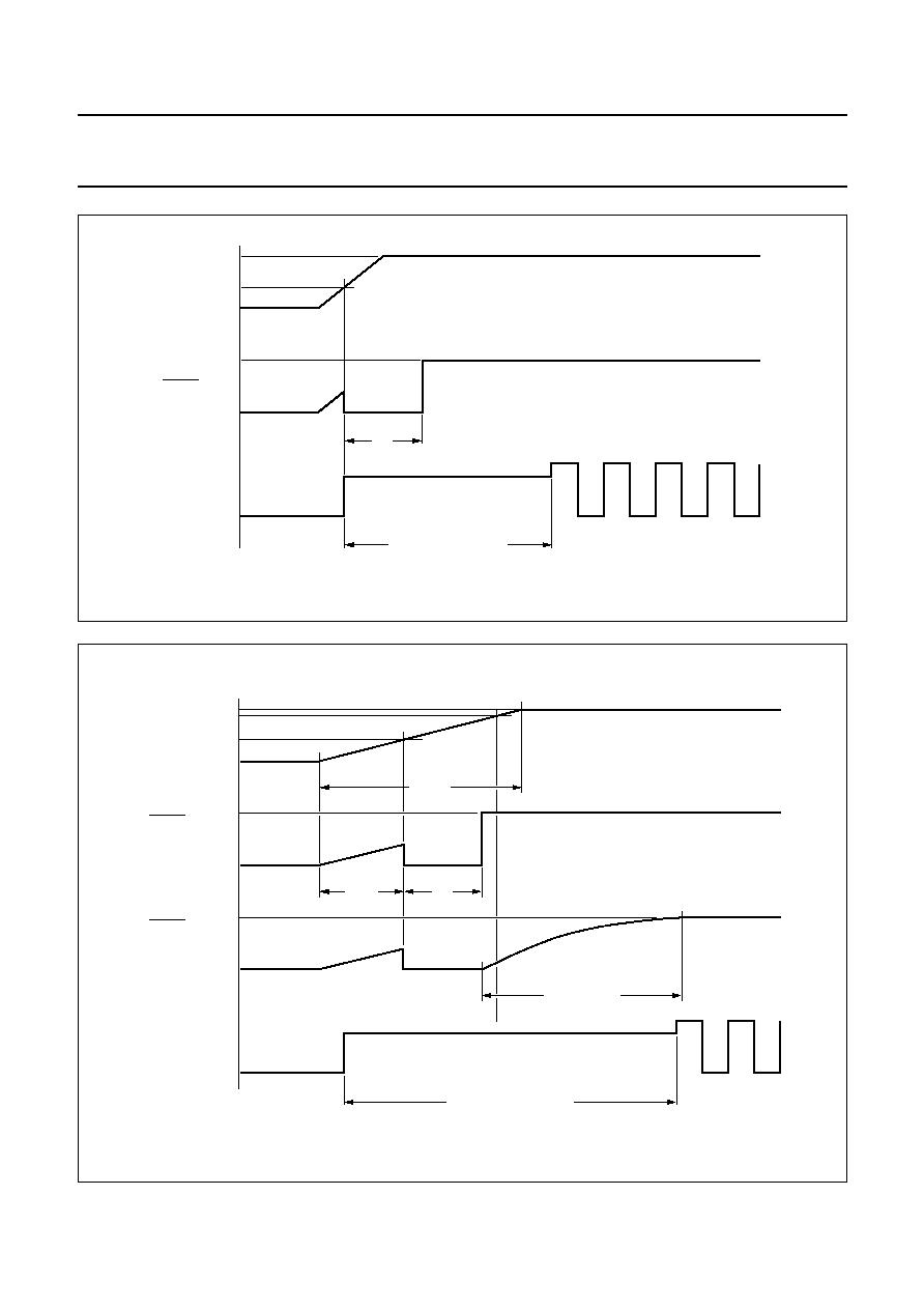
Fig.6 Reset with fast rising V
DD
.
handbook, full pagewidth
V
DD
VSS
Vref
VDD
V
DD
VSS
RESET
OSCILLATOR
oscillator start up time
td
MCD240
handbook, full pagewidth
VDD
V
SS
Vref
VDD
VSS
OSCILLATOR
oscillator start up time
td
Vmin
t Vref
RC
8
◊
tVDD
VDD
t
VDD
RESET
without
external
component
VSS
V
DD
RESET
with
external
component
MCD241
Fig.7 Reset with slow V
DD
.
1996 Nov 29
10
Philips Semiconductors
Product specification
8-bit microcontrollers with OSD and VST
84C44X; 84C64X; 84C84X
8
ANALOG CONTROL
8.1
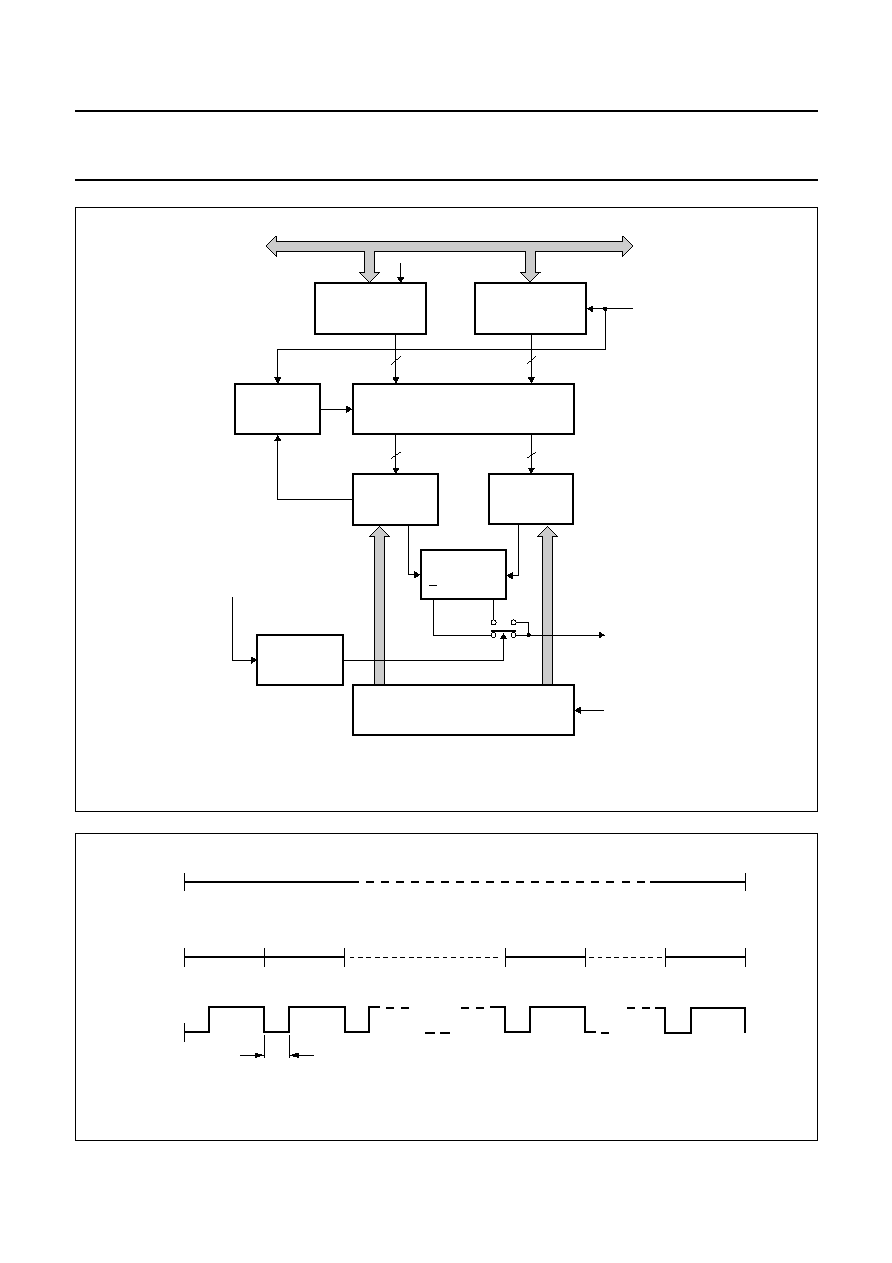
6-bit PWM DACs
Five PWM outputs are available for analog control
purposes e.g. volume, balance, brightness, saturation, etc.
The block diagram of a typical 6-bit PWM DAC is shown in
Fig.8. Each PWM output can generate pulses of
programmable length that have a repetition frequency of
1
/
64
◊
f
PWM
, where f
PWM
=
1
/
3
◊
f
XTAL
.
8.1.1
P
IN SELECTION FOR
PWM
OUTPUTS
The PWM outputs PWM1 to PWM5, share the same pins
as the Derivative Port lines DP0.1 to DP0.5.
Setting the (relevant PWM enable) bit PWMnE to:
∑
Logic 1, selects the relevant PWMx output function
∑
Logic 0, selects the relevant DP0.x Port function.
8.1.2
P
OLARITY OF THE
PWM
OUTPUTS
The polarity of all five PWM outputs is selected by the state
of the polarity control bit P6LVL.
Setting the control bit P6LVL to:
∑
Logic 0, sets the PWMx outputs to the default polarity
∑
Logic 1, inverts all the PWMx outputs.
8.1.3
A
NALOG OUTPUT VOLTAGE
A DC voltage proportional to the PWM control setting may
be obtained by connecting an integrating network to each
of the PWM outputs (see Fig.9).
The analog value is calculated as follows:
Where:
∑
∑
∑
∑
PWMDL is the decimal value of the contents of the
PWM data latch.
Therefore, the analog output voltage is:
V
A
t
HIGH
t
r
--------------
V
O
◊
=
t
HIGH
t
0
PWMDL
◊
HIGH time of the PWM pulse
=
=
t
r
t
0
64
◊
repetition time of the PWM pulse
=
=
t
0
3
f
XTAL
--------------
=
V
A
PWMDL
64
------------------------
V
O
◊
=
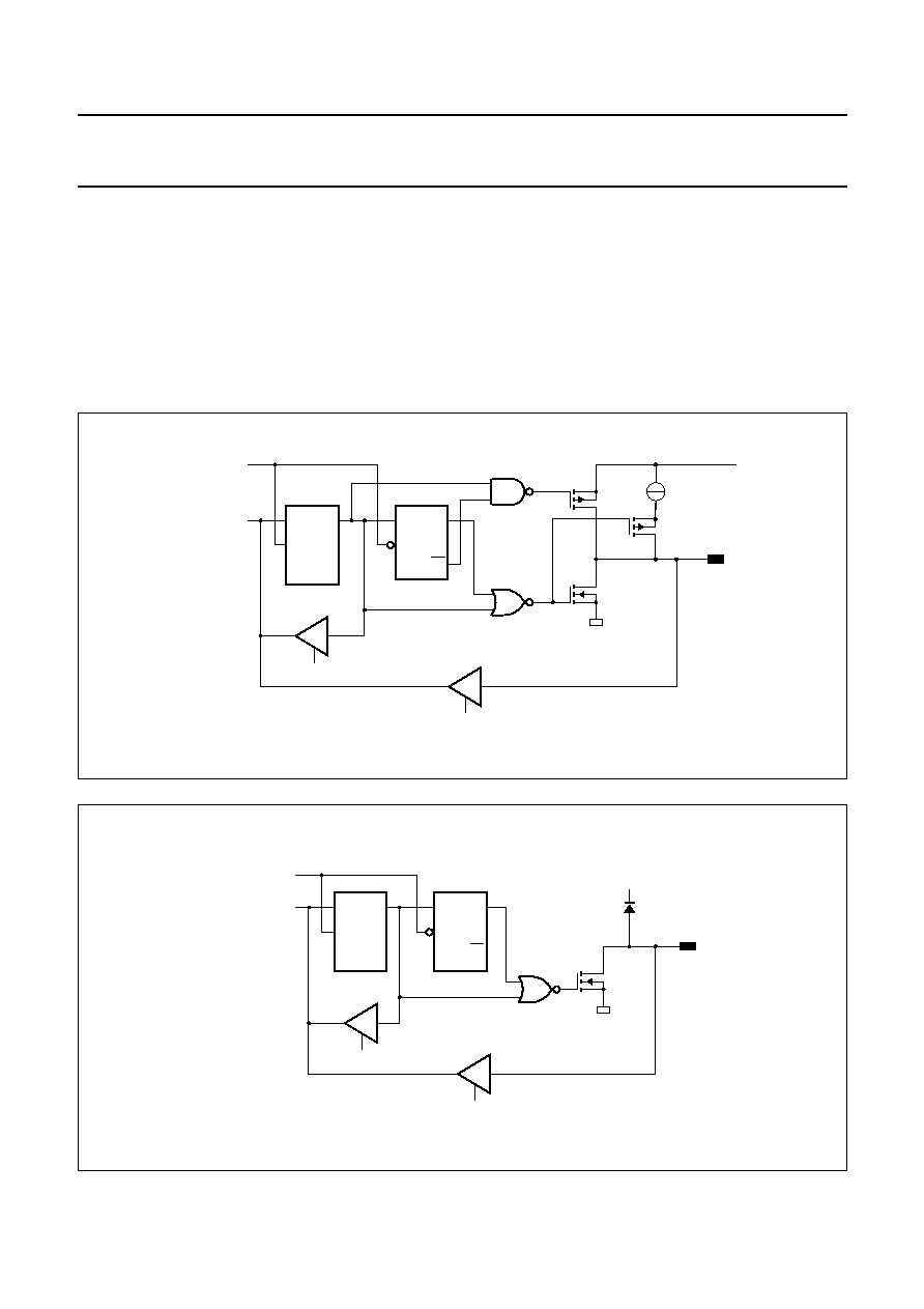
Fig.8 Block diagram of the 6-bit PWM DAC.
handbook, full pagewidth
MCD176
DP0.x data
I/O
DP0.x/PWMx
6-BIT PWM DATA LATCH
P6LVL
PWMnE
6-BIT DAC PWM
CONTROLLER
Q
Q
polarity control bit
f PWM
1996 Nov 29
11
Philips Semiconductors
Product specification
8-bit microcontrollers with OSD and VST
84C44X; 84C64X; 84C84X
Fig.9 PWM output patterns (P6LVL = 0).
handbook, full pagewidth
MCD175
00
01
m
63
f
PWM
2
decimal value PWM data latch
64
1
3
m
m
+
1
m
+
2
63
64
1
t 0
1996 Nov 29
12
Philips Semiconductors
Product specification
8-bit microcontrollers with OSD and VST
84C44X; 84C64X; 84C84X
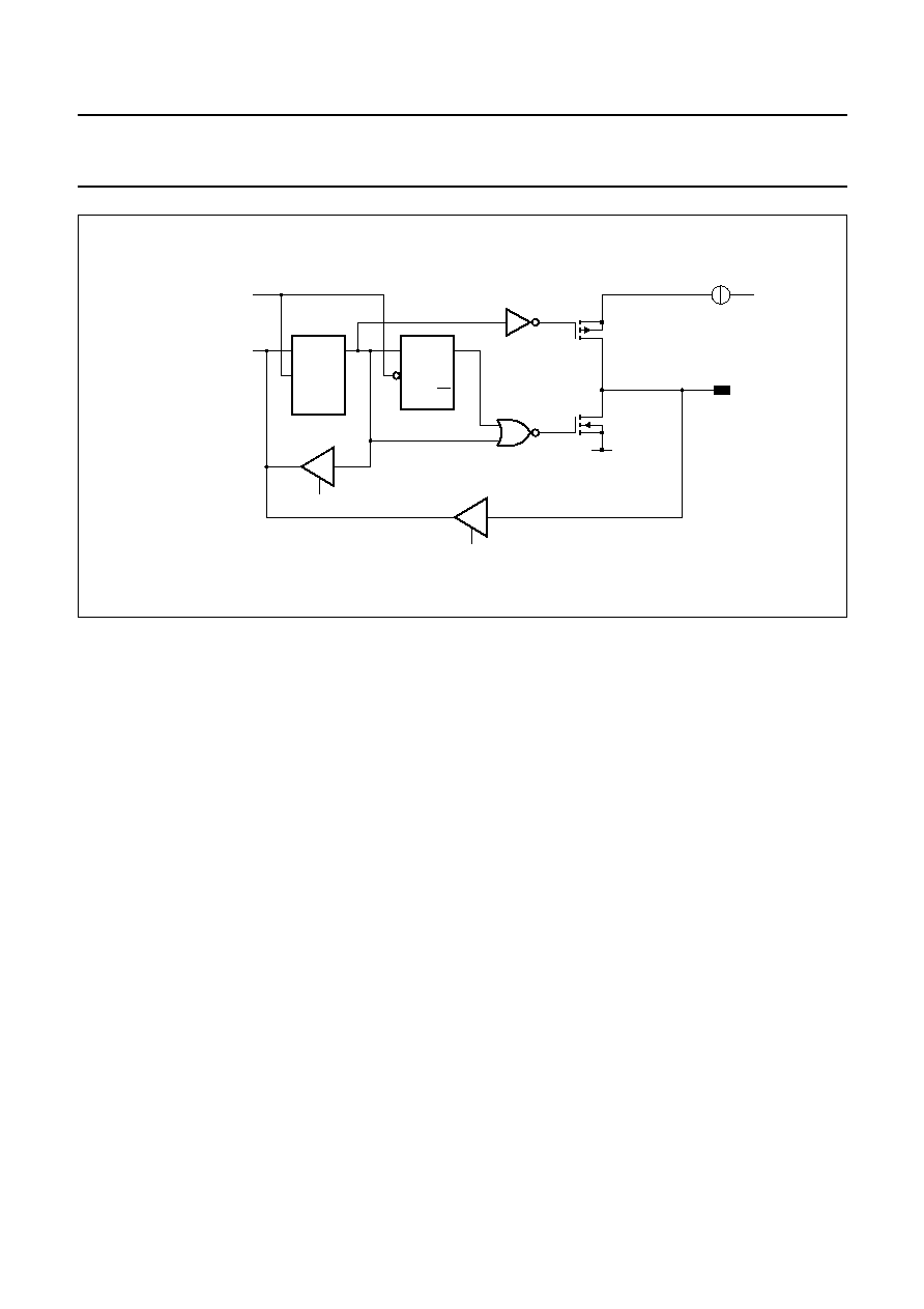
9
VST CONTROL
9.1
14-bit PWM DAC
The PCA84C640 has one 14-bit PWM DAC output (TDAC)
with a resolution of 16384 levels for Voltage Synthesized
Tuning. The PWM DAC (see Fig.10) consists of:
∑
14-bit counter
∑
Two 7-bit DAC interface data latches (VSTH and VSTL)
∑
One 14-bit DAC data latch (VSTREG)
∑
Pulse control.
The polarity of output TDAC is selected with bit P14LVL.
Setting the bit P14LVL to:
∑
Logic 1, sets the TDAC output to the default polarity
∑
Logic 0, inverts the TDAC output.
9.1.1
14-
BIT COUNTER
The counter is continuously running and is clocked by f
0
.
The period of the clock,
The repetition time for one complete cycle of the counter:
The repetition time for one cycle of the lower 7-bits of the
counter is:
Therefore, the number of t
sub
periods in a complete
cycle t
r
is:
9.1.2
D
ATA AND INTERFACE LATCHES
In order to ensure correct operation, interface data latch
VSTH is loaded first and then interface data latch VSTL.
The contents of:
∑
VSTH are used for coarse adjustment
∑
VSTL are used for fine adjustment.
At the beginning of the first t
sub
period following the loading
of VSTL, both data latches are loaded into data latch
VSTREG. After the contents of VSTH and VSTL are
latched into VSTREG, one t
sub
period is needed to
generate the appropriate pulse pattern.
To ensure correct DAC conversion, two (2) t
sub
periods
should be allowed before beginning the next sequence.
t
0
3
f
XTAL
--------------
=
t
r
t
0
16 384
◊
=
t
sub
t
0
128
◊
=
N
t
0
16 384
◊
t
0
128
◊
---------------------------
128
=
=
9.2
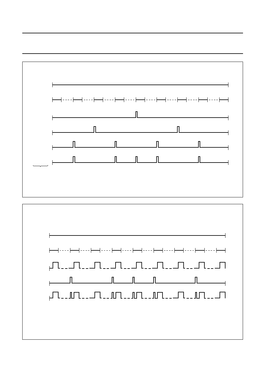
Coarse adjustment
The coarse adjustment output (OUT1) is reset to LOW
(inactive) at the start of each t
sub
period.
It will remain LOW until the time
has
elapsed and then will go HIGH and remain so until the next
t
sub
period starts.
9.3
Fine adjustment
Fine adjustment is achieved by generating additional
pulses at the start of particular sub-periods (t
subn
).
These additional pulses have a width of t
0
.
The sub-period in which a pulse is added is determined by
the contents of VSTL interface latch.
Table 3 gives the numbers of the t
subn
, at the start of which
an additional pulse is generated, depending on the bit in
VSTL being a logic 0. When more than one bit is a logic 0
a combination of additional pulses are generated.
For example, if VSTL = 1111010, which is a combination
of
∑
VSTL = 1111110: sub-period 64, and
∑
VSTL = 1111011: sub-periods 16, 48, 80 and 112,
then additional pulses will be given in sub-periods
16, 48, 64, 80 and 112; this is illustrated in Fig.12.
If VSTH = 0011101, VSTL = 1111010 and P14LVL = 0,
then the TDAC output is as shown in Fig.13.
Table 3
Additional pulse distribution
LOWER
7 BITS
(VSTL)
ADDITIONAL PULSE IN
SUB-PERIODS t
subn
111111
0
64
11111
0
1
32, 96
1111
0
11
16, 48, 80, 112
111
0
111
8, 24, 40, 56, 72, 88, 104, 120
11
0
1111
4, 12, 20, 28, 36, 44, 52, 60 .... 116, 124
1
0
11111
2, 6, 10, 14, 18, 22, 26, 30, .... 122, 126
0
111111
1, 3, 5, 7, 9, 11, 13, 15, 17, .... 125, 127
t
0
VSTH
1
+
(
)
◊
[
]
1996 Nov 29
13
Philips Semiconductors
Product specification
8-bit microcontrollers with OSD and VST
84C44X; 84C64X; 84C84X
handbook, full pagewidth
DATA LATCH VSTL
DATA LATCH VSTH
DAC DATA LATCH VSTREG
'MOV instruction'
'MOV instruction'
DATA LOAD
TIMING PULSE
COARSE PWM
FINE
OUT2
OUT1
ADD
Q
Q
P14LVL
14-BIT COUNTER
Q14 to Q8
Q7 to Q1
polarity
control bit
TDAC output
f0
MCD177
7
7
7
7
LOAD
Fig.10 Block diagram of the 14-bit PWM DAC.
Fig.11 Coarse adjustment output (OUT1).
andbook, full pagewidth
t r
t sub0
OUT 1
t sub1
t subn
t sub127
t0
◊
(VSTH
+
1)
MCD313
1996 Nov 29
14
Philips Semiconductors
Product specification
8-bit microcontrollers with OSD and VST
84C44X; 84C64X; 84C84X
Fig.12 Fine adjustment output (OUT2).
handbook, full pagewidth
MCD314
t sub0
t sub16
t sub32
t sub48
t sub64
t sub80
t sub96
t sub112
t sub127
t r
111 1110
111 1101
111 1011
111 1010
VSTL
Fig.13 TDAC output.
handbook, full pagewidth
MCD315
t r
t
sub0
OUT 1
OUT 2
TDAC
t
sub16
t
sub32
t
sub48
t
sub64
t
sub80
t
sub96
t
sub112
t
sub127
1996 Nov 29
15
Philips Semiconductors
Product specification
8-bit microcontrollers with OSD and VST
84C44X; 84C64X; 84C84X
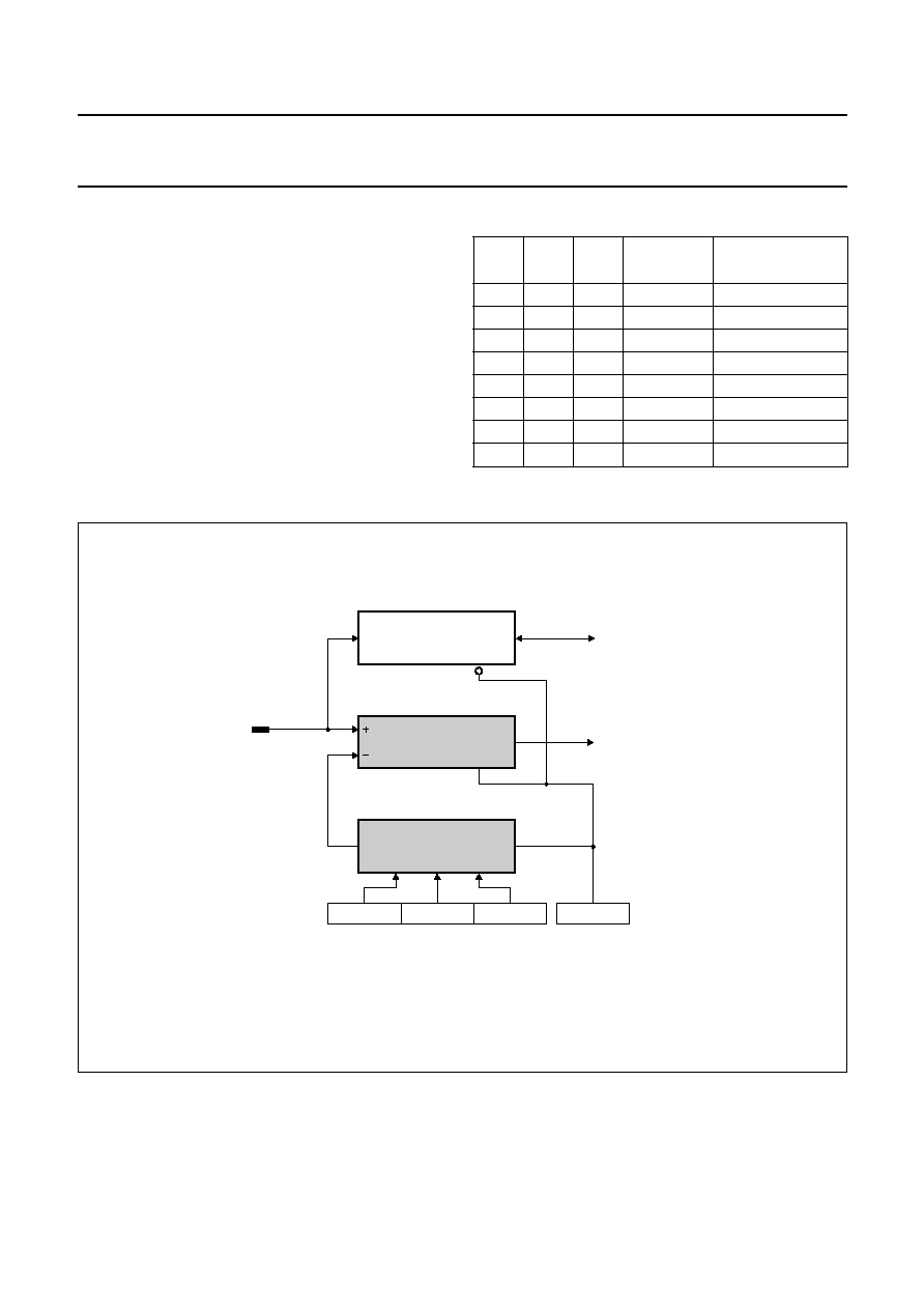
10 AFC INPUT
The AFC input is used to measure the level of the
Automatic Frequency Control signal. This is achieved by
comparing the AFC input signal with the output of a 3-bit
DAC as shown in Fig.14. DAC analog switches select one
of 8 resistor taps connected between V
DD
and V
SS
.
Consequently, eight different voltages may be selected
(see Table 4). The compare signal AFCC, can be tested to
determine whether the AFC input is higher or lower than
the DAC level.
The AFC input shares the same pin as the Derivative Port
line DP1.7. Setting the enable bit AFCE to:
∑
Logic 1, selects the AFC function
∑
Logic 0, selects the Derivative Port DP1.7 function.
Table 4
Selection of V
ref
AFC2 AFC1 AFC0
V
ref
V
ref
(for V
DD
= 5.0 V)
0
0
0
V
DD
◊
0.125
0.625 V
0
0
1
V
DD
◊
0.250
1.250 V
0
1
0
V
DD
◊
0.375
1.875 V
0
1
1
V
DD
◊
0.500
2.500 V
1
0
0
V
DD
◊
0.625
3.125 V
1
0
1
V
DD
◊
0.750
3.750 V
1
1
0
V
DD
◊
0.875
4.375 V
1
1
1
V
DD
5.000 V
handbook, full pagewidth
COMPARATOR
3-BIT DAC
EN
EN
DP1.7/AFC
AFC2
AFC1
AFC0
AFCE
AFCC
internal bus
inner latches
DP1.7
MCD178
Fig.14 AFC circuit.
1996 Nov 29
16
Philips Semiconductors
Product specification
8-bit microcontrollers with OSD and VST
84C44X; 84C64X; 84C84X
11 INPUT/OUTPUT (I/O)
Each parallel I/O port line may be individually configured
using one of three possible I/O mask options.
The three I/O mask options are specified below:
Option 1 Standard port with switched pull-up current
source, Fig.15.
Option 2 Open drain, Fig.16.
Option 3 Push-pull (output only), Fig.17.
Table 5 specifies the possible port option list. When these
devices are used for emulation purposes, in order to match
the piggy back device provided it is recommended that the
port options listed in Table 6 are used.
handbook, full pagewidth
MLA696
TR3
I/O PORT
LINE
SLAVE
D
SQ
SQ
MASTER
D
MQ
WRITE PULSE
OUTL/ORL/ANL/MOV
DATA BUS
ORL/ANL/MOV
IN/MOV
TR1
VSS
TR2
VDD
constant
current
source
100
µ
A typ.
Fig.15 Standard output with switched pull-up current source (Option 1).
handbook, full pagewidth
MLA697
I/O PORT
LINE
SLAVE
D
SQ
SQ
MASTER
D
MQ
WRITE PULSE
OUTL/ORL/ANL
DATA BUS
ORL/ANL
IN
TR1
VSS
VDD
Fig.16 Open drain type I/O (Option 2).
1996 Nov 29
17
Philips Semiconductors
Product specification
8-bit microcontrollers with OSD and VST
84C44X; 84C64X; 84C84X
handbook, full pagewidth
MGD864
OUTPUT
LINE
SLAVE
D
SQ
SQ
MASTER
D
MQ
WRITE PULSE
OUTL/OR /ANL
DATA BUS
ORL/ANL
IN
TR1
VSS
TR2
VDD
constant
current
source
100
µ
A typ.
Fig.17 Push-pull type output (Option 3).
1996 Nov 29
18
Philips Semiconductors
Product specification
8-bit microcontrollers with OSD and VST
84C44X; 84C64X; 84C84X
Table 5
User mask programmable port option list
Notes
1. Each pin can be configured to a HIGH (S) or LOW (R)
state after power-on-reset. The required state of each
pin is therefore specified by R or S.
2. DP1.4 available only with the PCA84C440,
PCA84C443, PCA84C640, PCA84C643,
PCA84C840 and PCA84C843.
PORT
PIN
OPTION
(1)
P0.0
13
P0.1
14
P0.2
15
P0.3
16
P0.4
17
P0.5
18
P0.6
19
P0.7
20
P1.0
7
P1.1
8
P1.2
10
P1.3
11
P1.4
12
DP0.0
1
DP0.1
2
DP0.2
3
DP0.3
4
DP0.4
5
DP0.5
6
DP0.6
40
DP0.7
39
DP1.0
41
DP1.1
38
DP1.2
37
DP1.3
36
DP1.4
(2)
34
DP1.5
23
DP1.6
22
DP1.7
9
VOB
25
3
R
VOW3
24
3
R
Table 6
Port options for the 84C640 in emulation mode
PORT
PIN
OPTION
P0.0
13
1
S
P0.1
14
1
S
P0.2
15
1
S
P0.3
16
1
S
P0.4
17
1
S
P0.5
18
1
S
P0.6
19
1
S
P0.7
20
1
S
P1.0
7
1
S
P1.1
8
1
S
P1.2
10
1
S
P1.3
11
1
S
P1.4
12
1
S
DP0.0
1
DP0.1
2
DP0.2
3
DP0.3
4
DP0.4
5
DP0.5
6
DP0.6
40
2
S
DP0.7
39
2
S
DP1.0
41
DP1.1
38
DP1.2
37
DP1.3
36
DP1.4
34
DP1.5
23
DP1.6
22
DP1.7
9
VOB
25
3
R
VOW3
24
3
R

1996 Nov 29
19
Philips Semiconductors
Product specification
8-bit microcontrollers with OSD and VST
84C44X; 84C64X; 84C84X
12 ON SCREEN DISPLAY
12.1
Features
∑
Display format: 2 rows
◊
16 characters
∑
Software controlled vertical and horizontal display
position
∑
64 different (mask programmable) characters in ROM
∑
Black box background
∑
Four programmable display character sizes
∑
Four programmable character dot matrix sizes:
≠ 6
◊
9 and 6
◊
13
≠ 8
◊
9 and 8
◊
13
∑
Half-dot rounding for the whole screen
∑
4 from 7 colours possible on screen
∑
Clock generator for On Screen Display function with:
≠ RC oscillator
≠ LC oscillator,
for the various types of PCA84C44X; 84C64X; 84C84X.
12.2
Horizontal display position control
The horizontal position counter is incremented every OSD
cycle after the programmed level of HSYNCN occurs at the
HSYNCN pin. The counter is reset when the opposite
polarity of the HSYNCN pulse is reached.
12.3
Vertical display position control
The vertical position counter is incremented every
HSYNCN cycle and is reset by the VSYNCN signal.
12.4
Clock generator
There are two types of oscillators available for the various
types. The oscillator is triggered on the trailing edge of
HSYNCN when the OSD logic is enabled and stops on the
following leading edge of HSYNCN.
The OSD oscillator must be externally adjusted to the
desired frequency (decreasing the OSD frequency gives
broader characters). Before the oscillation frequency can
be adjusted HSYNCN must be HIGH (if HLVL = 1).
Oscillation stops by setting the HSYNCN pin LOW when
HLVL = 1.
12.4.1
RC
OSCILLATOR
The RC oscillator is available in the types:
PCA84C440; 84C443; 84C640; 84C643;
84C840; 84C843.
The external RC network is connected between
pin 28 and V
SS
(see Fig.19).
12.4.2
LC
OSCILLATOR
The LC oscillator is available in the types:
PCA84C441; 84C444; 84C641; 84C644;
84C841; 84C844.
The external LC network is connected between
pins 28 and 29 (see Fig.20).
1996 Nov 29
20
Philips Semiconductors
Product specification
8-bit microcontrollers with OSD and VST
84C44X; 84C64X; 84C84X
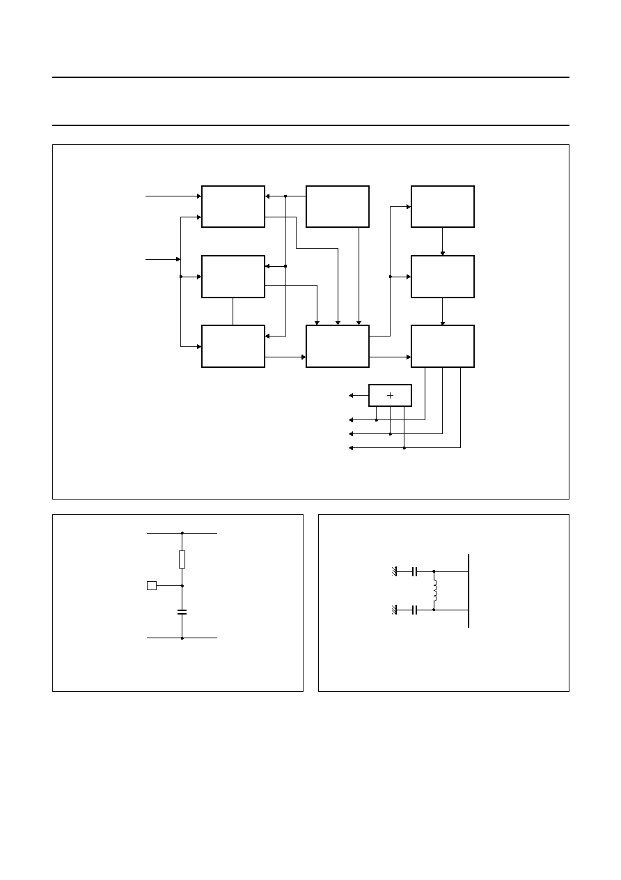
handbook, full pagewidth
HORIZONTAL
DISPLAY
POSITION
CONTROL
VERTICAL
DISPLAY
POSITION
CONTROL
DISPLAY
CONTROL
MEMORY
DISPLAY
CHARACTER
DATA
MEMORY
CLOCK
GENERATOR
CONTROL
TIMING
GENERATOR
DISPLAY
CONTROL
CHARACTER
ROM
HSYNCN
VSYNCN
VOW3
VOW2
VOW1
VOB
MCD179
(1)
Fig.18 OSD block diagram.
(1) See Figs 19 and 20 for connection of external components.
handbook, halfpage
VSS
DD
V
R
C
DOSC1
MCD173
Fig.19 RC oscillator.
Fig.20 LC oscillator.
handbook, halfpage
MCD247
C1
DOSC1
L1
C2
DOSC2
1996 Nov 29
21
Philips Semiconductors
Product specification
8-bit microcontrollers with OSD and VST
84C44X; 84C64X; 84C84X
12.5
Display data registers
The display data registers consists of a group of 32 derivative registers located at addresses 20H to 3FH inclusive
(see Table 7). At power-up the contents of the display data registers are undefined.
The format of each display data register is shown in Table 8, and their functions described in Table 9.
Table 7
Display data registers addresses
Table 8
Display data register (address 20H to 3FH)
Table 9
Description of display data register bits
12.6
Display control registers
The display control registers consists of a group of 6 derivative registers located at addresses 40H to 45H inclusive
(see Table 10). Each register may be read from or written to. After a reset operation the contents of the display control
registers are zero.
Table 10 Display control registers addresses
ADDRESS
DISPLAY DATA FOR
BIT 7
BIT 6
BIT 5
BIT 4
BIT 3
BIT 2
BIT 1
BIT 0
20H to 2FH
Row 0 = the first display row
CC1
CC0
MD5
MD4
MD3
MD2
MD1
MD0
30H to 3FH
Row 1 = the second display row
7
6
5
4
3
2
1
0
CC1
CC0
MD5
MD4
MD3
MD2
MD1
MD0
BIT
SYMBOL
DESCRIPTION
7
CC1
Colour code. The state of these two bits enable individual characters to be displayed in
one of four colours. See Tables 24, 25 and 26.
6
CC0
5
MD5
Character code.
The character set is stored in ROM and consists of 64 different characters.
The selection of each character is dependent on the state of the 6 bits, MD0 to MD5.
4
MD4
3
MD3
2
MD2
1
MD1
0
MD0
ADDRESS
REGISTER
BIT 7
BIT 6
BIT 5
BIT 4
BIT 3
BIT 2
BIT 1
BIT 0
40H
OSDCA
CC34
CC24
CC14
RBLK
ROUND
STBY
VLVL
HLVL
41H
LINE 0A
SZ01
SZ00
VP05
VP04
VP03
VP02
VP01
VP00
42H
LINE 0B
BLK0
VB0
HP05
HP04
HP03
HP02
HP01
HP00
43H
OSDCB
CDTW
CDTH
CC33
CC23
CC32
CC12
CC21
CC11
44H
LINE 1A
SZ11
SZ10
VP15
VP14
VP13
VP12
VP11
VP10
45H
LINE 1B
BLK1
VB1
HP15
HP14
HP13
HP12
HP11
HP10
1996 Nov 29
22
Philips Semiconductors
Product specification
8-bit microcontrollers with OSD and VST
84C44X; 84C64X; 84C84X
12.6.1
D
ERIVATIVE REGISTER
OSDCA
Table 11 Derivative register OSDCA (address 40H)
Table 12 Description of OSCDA bits
7
6
5
4
3
2
1
0
CC34
CC24
CC14
RBLK
ROUND
STBY
VLVL
HLVL
BIT SYMBOL
DESCRIPTION
7
CC34
Character colour code bits.
These bits are used for colour selection purposes. See Table 24.
6
CC24
5
CC14
4
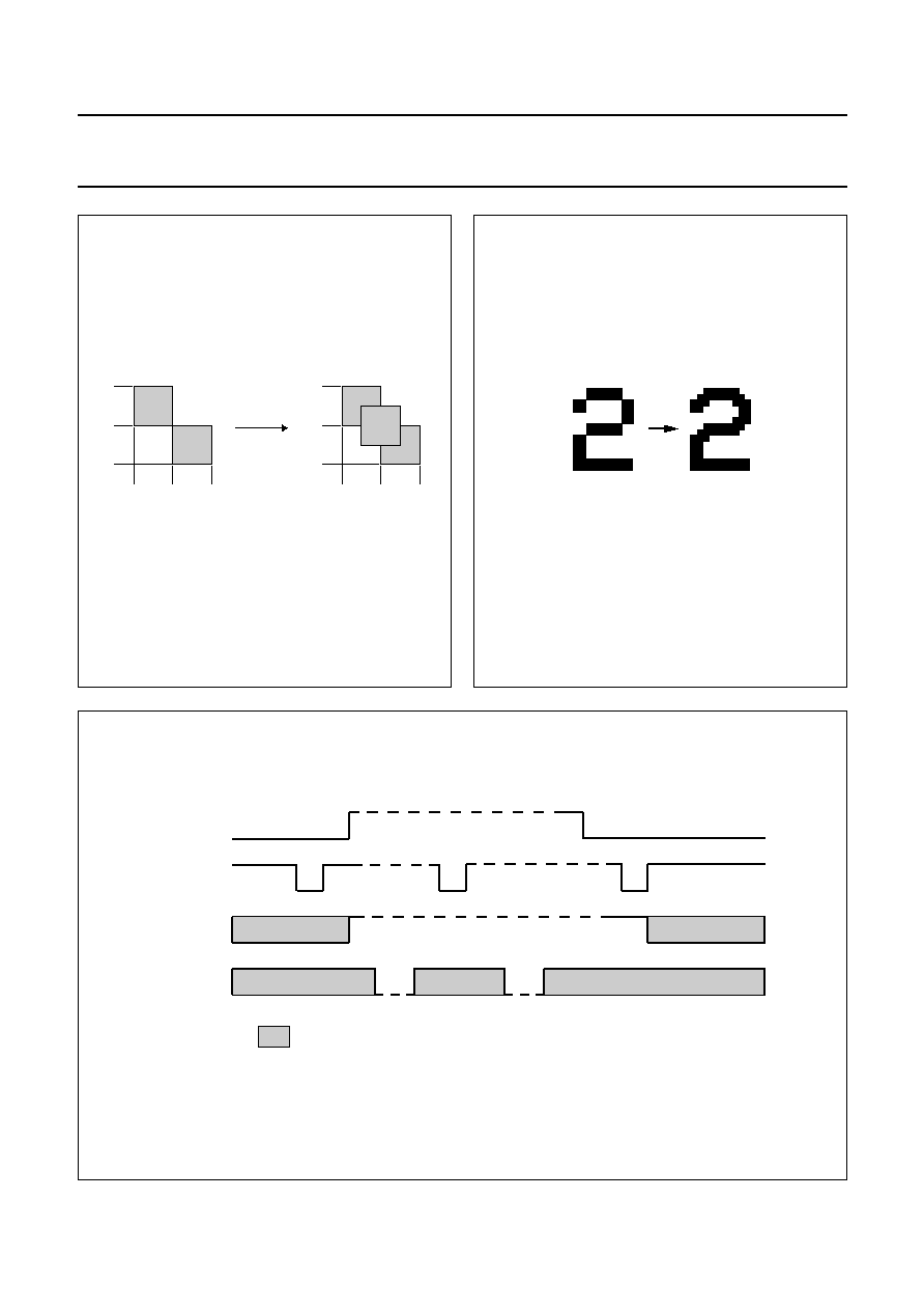
RBLK
Raster blanking control (see Fig.24). When the RBLK bit is:
Logic 1, the VOB output is driven HIGH to display the OSD characters on a blank screen.
Logic 0, the VOB output returns to its normal output state on the trailing edge of VSYNCN.
3
ROUND
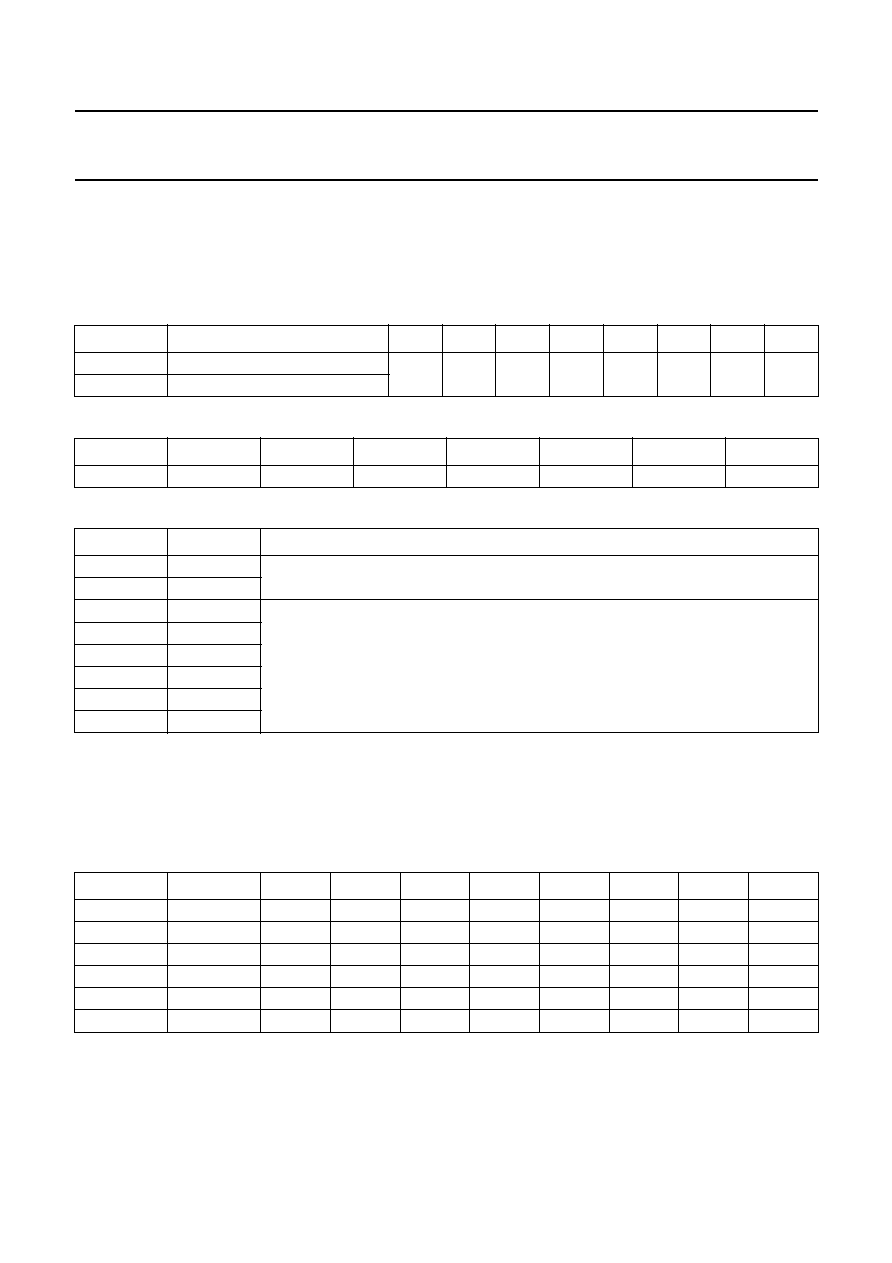
Character rounding control (see Figs 22 and 23). The rounding function generates half dots where
the corners of two dots meet. The rounding function also works with multiple cell characters.
When the ROUND bit is:
Logic 1, the rounding function is enabled.
Logic 0, the rounding function is disabled.
2
STBY
Stand-by. This bit is used to enable or disable the OSD facility. When the STBY bit is:
Logic 1, the OSD oscillator is disabled.
Logic 0, the OSD oscillator is enabled and the OSD facility is available.
1
VLVL
Vertical synchronous signal level (see Fig.21).
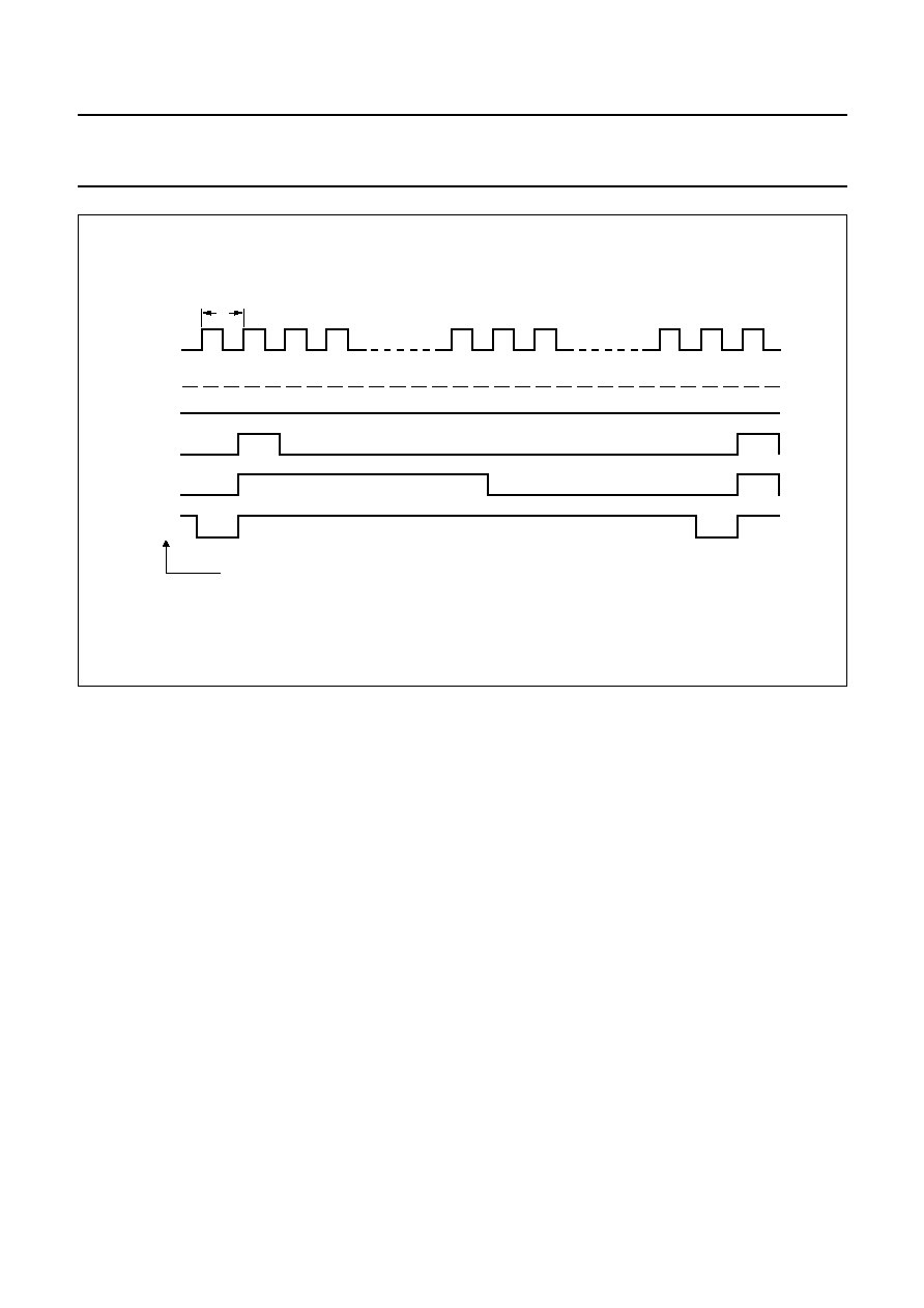
This bit selects the active level of the VSYNCN input signal. When the VLVL bit is:
Logic 1, VSYNCN is active HIGH.
Logic 0, VSYNCN is active LOW.
0
HLVL
Horizontal synchronous signal level (see Fig.21).
This bit selects the active level of the HSYNCN input signal. When the HLVL bit is:
Logic 1, HSYNCN is active HIGH.
Logic 0, HSYNCN is active LOW.
Fig.21 VSYNCN and HSYNCN active level.
handbook, full pagewidth
(VSYNCN)
HSYNCN
(HLVL = VLVL = 0)
(HLVL = VLVL = 1)
characters can be displayed
(VSYNCN)
HSYNCN
MCD180
1996 Nov 29
23
Philips Semiconductors
Product specification
8-bit microcontrollers with OSD and VST
84C44X; 84C64X; 84C84X
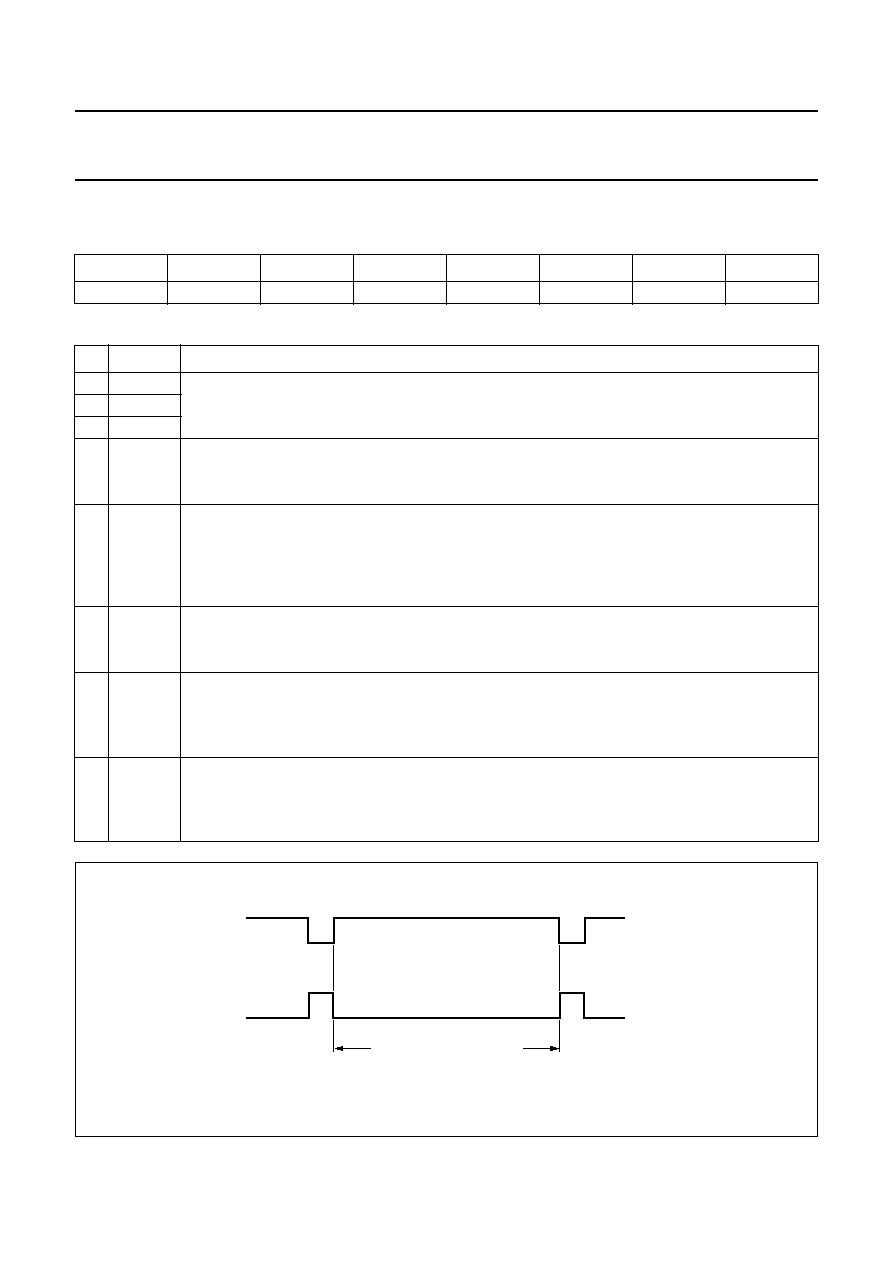
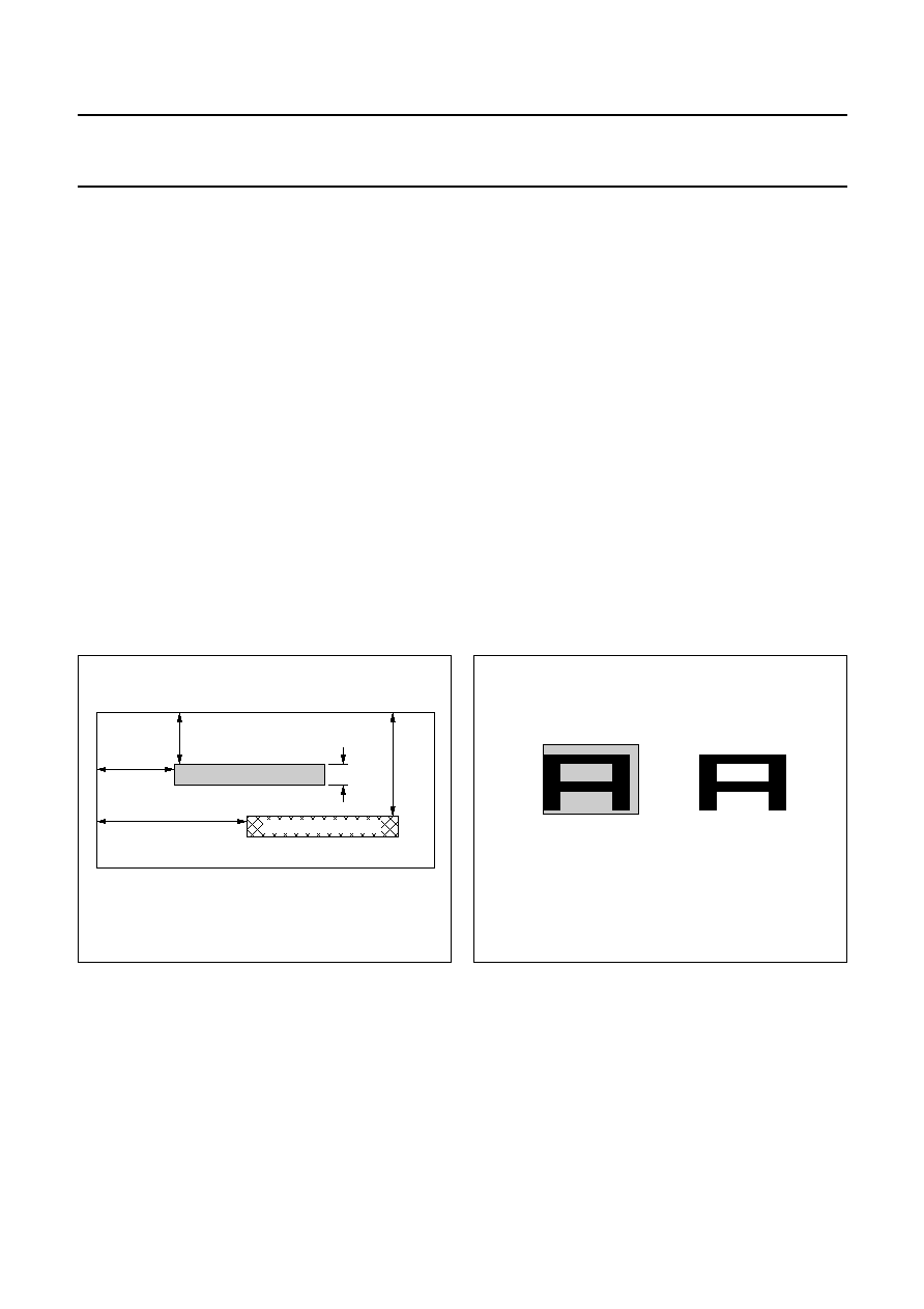
Fig.22 Rounding function.
ROUND = 1
ROUND = 0
T
T
T
H
H
H
T
T
T
H
H
H
MCD246
Fig.23 Rounding effect.
handbook, halfpage
MCD181
Fig.24 Raster blanking timing RLBK.
handbook, full pagewidth
MCD316
RBLK
VSYNCN
VOB
VOW1, 2, 3
= normal output

1996 Nov 29
24
Philips Semiconductors
Product specification
8-bit microcontrollers with OSD and VST
84C44X; 84C64X; 84C84X
12.6.2
D
ERIVATIVE REGISTERS
LINE 0A
AND
LINE 0B
Table 13 Derivative register LINE 0A (address 41H)
Table 14 Description of LINE 0A bits
Table 15 Derivative register LINE 0B (address 42H)
Table 16 Description of LINE 0B bits
REGISTER
FUNCTION
LINE 0A
Determine the character size and vertical position of Row 0 (the first display row).
LINE 0B
Determine the horizontal position of Row 0 and the selection of background and blanking functions.
7
6
5
4
3
2
1
0
SZ01
SZ00
VP05
VP04
VP03
VP02
VP01
VP00
BIT SYMBOL
DESCRIPTION
7
SZ01
Character size. The state of these two bits enable one of four possible character sizes to be
selected for Row 0. Character sizes include background. See Table 23.
6
SZ00
5
VP05
Vertical position control.
The vertical position of Row 0 is selected by the state of the 6 bits, VP00 to VP05.
For details see Section 12.7.1 "Vertical position".
4
VP04
3
VP03
2
VP02
1
VP01
0
VP00
7
6
5
4
3
2
1
0
BLK0
VB0
HP05
HP04
HP03
HP02
HP01
HP00
BIT SYMBOL
DESCRIPTION
7
BLK0
Blanking. This bit enables or disables the character display. When BLK0 is set to:
Logic 1, the outputs VOW1, VOW2, VOW3 and VOB are enabled; characters are displayed.
Logic 0, the outputs VOW1, VOW2, VOW3 and VOB are disabled; no characters are displayed.
6
VB0
Background. This bit determines whether the background display is selected or not.
The visual effect of background versus no background is shown in Fig.26. When VB0 is set to:
Logic 1, the characters in this row are displayed with background.
Logic 0, the background is disabled and only the characters are displayed.
5
HP05
Horizontal position control.
These 6 bits determine the start position of Row 0.
The horizontal position control is only active during OSDC clock cycles.
For details Section 12.7.2 "Horizontal position" and Fig.25.
4
HP04
3
HP03
2
HP02
1
HP01
0
HP00
1996 Nov 29
25
Philips Semiconductors
Product specification
8-bit microcontrollers with OSD and VST
84C44X; 84C64X; 84C84X
12.6.3
D
ERIVATIVE REGISTERS
LINE 1A
AND
LINE 1B
Table 17 Derivative register LINE 1A (address 44H)
Table 18 Description of LINE 1A bits
Table 19 Derivative register LINE 1B (address 45H)
Table 20 Description of LINE 1B bits
REGISTER
FUNCTION
LINE 1A
Determine the character size and vertical position of Row 1 (the second display row).
LINE 1B
Determine the horizontal position of Row 1 and the selection of background and blanking functions.
7
6
5
4
3
2
1
0
SZ11
SZ10
VP15
VP14
VP13
VP12
VP11
VP10
BIT SYMBOL
DESCRIPTION
7
SZ11
Character size. The state of these two bits enable one of four possible character sizes to be
selected for Row 1. Character sizes include background. See Table 23.
6
SZ10
5
VP15
Vertical position control.
The vertical position of Row 1 is selected by the state of the 6 bits, VP10 to VP15.
For details see Section 12.7.1 "Vertical position".
4
VP14
3
VP13
2
VP12
1
VP11
0
VP10
7
6
5
4
3
2
1
0
BLK1
VB1
HP15
HP14
HP13
HP12
HP11
HP10
BIT SYMBOL
DESCRIPTION
7
BLK1
Blanking. This bit enables or disables the character display. When BLK1 is:
Logic 0, the outputs VOW1, VOW2, VOW3 and VOB are disabled; no characters are displayed.
Logic 1, the outputs VOW1, VOW2, VOW3 and VOB are enabled; characters are displayed.
6
VB1
Background. This bit determines whether the background display is selected or not.
The visual effect of background versus no background is shown in Fig.26. When VB1 is set to:
Logic 1, the characters in this line are displayed with background.
Logic 0, the background is disabled and only the character is displayed.
5
HP15
Horizontal position control.
These 6 bits determine the start position of Row 1.
The horizontal position control is only active during OSDC clock cycles.
For details Section 12.7.2 "Horizontal position" and Fig.25.
4
HP14
3
HP13
2
HP12
1
HP11
0
HP10
1996 Nov 29
26
Philips Semiconductors
Product specification
8-bit microcontrollers with OSD and VST
84C44X; 84C64X; 84C84X
12.6.4
D
ERIVATIVE REGISTER
OSDCB
Table 21 Derivative register OSDCB (address 43H)
Table 22 Description of OSDCB bits
REGISTER
FUNCTION
OSDCB
Determine the selection of:
∑
The size of the dot matrix grid
∑
Four colours from a possible seven for the display.
7
6
5
4
3
2
1
0
CDTW
CDTH
CC33
CC23
CC32
CC12
CC21
CC11
BIT SYMBOL
DESCRIPTION
7
CDTW
Character dot width control.The state of this bit determines the dot width of the character. When
the CDTW bit is set to:
Logic 1, the character width is 6 dots.
Logic 0, the character width is 8 dots.
6
CDTH
Character dot height control. The state of this bit determines the dot height of the character. When
the CDTH bit is set to:
Logic 1, the character height is 13 dots.
Logic 0, the character height is 9 dots.
5
CC33
Colour control bits.
In every VSYNCN cycle one screen can select any 4 colours from 7 and in addition a blank or black
screen. Combinations of CC1X, CC2X and CC3X control the character outputs VOW1, VOW2 and
VOW3 as shown in Table 24.
4
CC23
3
CC32
2
CC12
1
CC21
0
CC11
1996 Nov 29
27
Philips Semiconductors
Product specification
8-bit microcontrollers with OSD and VST
84C44X; 84C64X; 84C84X
12.7
OSD display position
12.7.1
V
ERTICAL POSITION
The line number of the vertical start position for:
∑
Row 0 is 4
◊
(VP00
VP05)
∑
Row 1 is 4
◊
(VP10
VP15).
Where:
∑
(VP00
VP05) = the decimal value of VP00
VP05
∑
(VP10
VP15) = the decimal value of VP10
VP15.
The character height in:
∑
Row 0 is H0 and is a function of the number of dots per
character and the state of the size control bits
SZ00 and SZ01
∑
Row 1 is H1 and is a function of the number of dots per
character and the state of the size control bits
SZ10 and SZ11.
Row 0 and Row 1 must not overlap each other and
therefore: VP1
(VP0 + H0); see Fig.25.
The four possible character heights are shown in Table 23.
12.7.2
H
ORIZONTAL POSITION
The horizontal start position (HP) of,
∑
Row 0: HP0 = 4
◊
(HP00
HP05) + 5
◊
t
OSCD
∑
Row 1: HP1 = 4
◊
(HP10
HP15) + 5
◊
t
OSCD
Where:
∑
(HP00
HP05) = the decimal value of HP00
HP05
and (HP00
HP05) > 10
∑
(HP10
HP15) = the decimal value of HP10
HP15
and (HP10
HP15) > 10
∑
t
OSCD
= one OSCD clock period.
Therefore for both Row 0 and Row 1,
HP0, HP1
45
◊
t
OSCD
.
ROW 0 CHARACTERS
VP0
HP0
H0
HP1
VP1
MCD183
ROW 1 CHARACTERS
Fig.25 Display position.
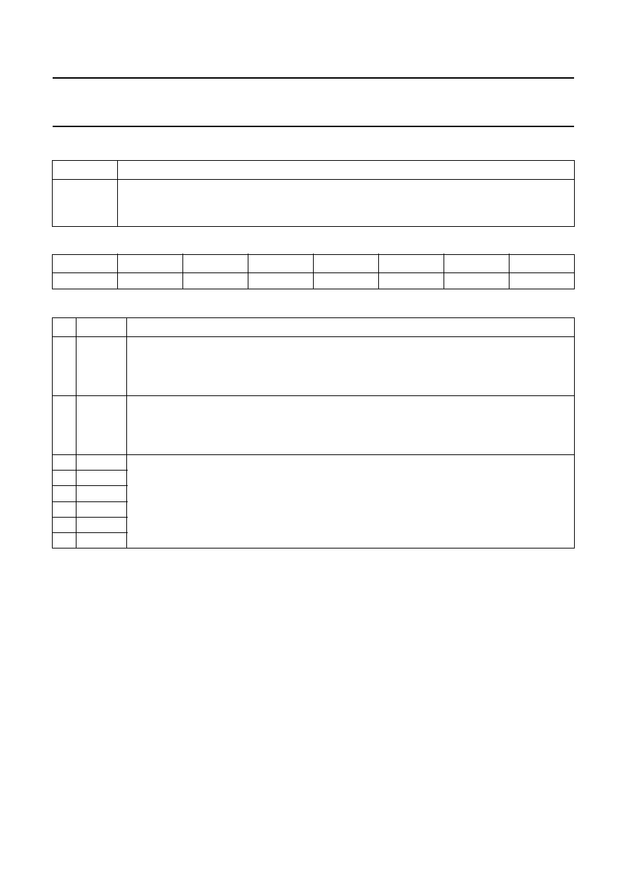
Fig.26 Background versus no background.
handbook, halfpage
with background
without background
MCD182
1996 Nov 29
28
Philips Semiconductors
Product specification
8-bit microcontrollers with OSD and VST
84C44X; 84C64X; 84C84X
12.8
OSD character size and colour selection
12.8.1
C
HARACTER SIZE
The character sizes are determined by the bits:
∑
CDTW, for the width
∑
CDTH, for the height.
The character sizes are selected by bits SZn1 and SZn0,
which denotes:
∑
SZ01 and SZ00 for Row 0
∑
SZ11 and SZ10 for Row 1.
Table 23 Character sizes selection
H denotes one horizontal line, T denotes one OSDC clock period and D denotes dots per character width/height.
SIZE BITS
CHARACTER SIZE
DOT MATRIX POINT
SZn1
SZn0
VERTICAL
HORIZONTAL
VERTICAL
HORIZONTAL
9D
13D
6D
8D
0
0
18H
26H
12T
16T
2H
2T
0
1
36H
52H
24T
32T
4H
4T
1
0
54H
78H
36T
48T
6H
6T
1
1
72H
104H
48T
64T
8H
8T
12.8.2
C
OLOUR SELECTION
Colour selection is achieved using bits in the,
∑
OSDCA register: CC34, CC24 and CC14
∑
OSDCB register: CC33, CC23, CC32, CC12,
CC21, and CC11
∑
Display data registers: CC1 and CC0.
In this way every combination of four colours can be made
(black and white can not be displayed at the same time).
The user may choose one colour out of each block.
Table 24 shows the selection of the output combinations.
Tables 25 and 26 show the possible colour combinations.
Fig.27 Colour control.
handbook, full pagewidth
CHARACTER ROM
DISPLAY DATA
MEMORY
DISPLAY CIRCUIT
CONTROL REGISTERS
VOW3
VOB
OR
CC1
CC0
CCxx
dot
background control
VOW2
VOW1
MCD184
OUTPUT
CONTROL
LOGIC
1996 Nov 29
29
Philips Semiconductors
Product specification
8-bit microcontrollers with OSD and VST
84C44X; 84C64X; 84C84X
Table 24 Character colour control
Table 25 Possible colour combinations
Table 26 Possible colour combinations (continued)
COLOUR CODE
CHARACTER OUTPUT PINS
CC1
CC0
VOW1 (Red)
VOW2 (Green)
VOW3 (Blue)
0
0
CC11
CC21
CC11 + CC21
0
1
CC12
CC12 + CC32
CC32
1
0
CC23 + CC33
CC23
CC33
1
1
CC14
CC24
CC34
COLOUR
(CC1, CC0) = (0, 0)
(CC1, CC0) = (0, 1)
(CC1, CC0) = (1, 0)
VOW1
VOW2
VOW3
VOW1
VOW2
VOW3
VOW1
VOW2
VOW3
CC11
CC21
CC11 + CC21
CC12
CC12 + CC32
CC32
CC12
CC12 + CC32
CC32
Blue
0
0
1
0
0
1
0
0
1
Green
0
1
0
0
1
0
0
1
0
Red
1
0
0
1
0
0
1
0
0
Yellow
1
1
0
-
-
-
-
-
-
Magenta
-
-
-
1
0
1
-
-
-
Cyan
-
-
-
-
-
-
0
1
1
COLOUR
(CC1, CC0) = (1, 1)
VOW1
VOW2
VOW3
CC14
CC24
CC34
Blue
0
0
1
Green
0
1
0
Red
1
0
0
Yellow
1
1
0
Magenta
1
0
1
Cyan
0
1
1
White
1
1
1
Black
0
0
0
1996 Nov 29
30
Philips Semiconductors
Product specification
8-bit microcontrollers with OSD and VST
84C44X; 84C64X; 84C84X
12.9
Character ROM
Character ROM contains the dot character fonts.
13
◊
8 dots are reserved for each character, regardless of
the dot matrix size actually selected.
The dot matrix grid is shown in Fig.28.
Philips provides a software under MS DOS environment
(IBM/PC or compatible) to help customer to design the
character font on the screen and to generate the bit pattern
HEX decimal file automatically.
Contact your local Philips Sales Organization for details.
handbook, halfpage
MCD185
1
2
3
4
5
6
7
8
13
12
10
9
1
2
3
4
5
6
7
8
11
Fig.28 Character ROM.
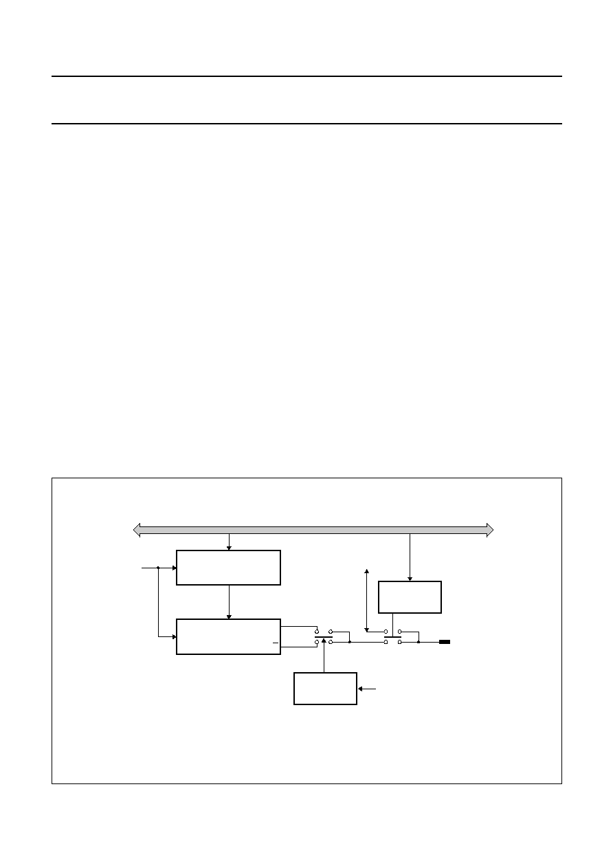
13 EMULATION MODE
The emulation mode configuration is shown in Fig.29.
In the emulation mode configuration the PCA84C640's
CPU is disabled and only its derivative logic is active.
The device is controlled by the PCF84C00 bond-out chip.
The PCA84C640's two derivative ports act as additional
ports for the PCF84C00. The interaction between the two
devices is as follows:
1. During the first machine cycle the PCF84C00 fetches
an instruction from EPROM and then decodes that
instruction.
2. During the second machine cycle the PCF84C00
executes the decoded instruction. If the instruction is
related to the derivative ports then DXALE, DXRDN
and/or DXWRN become active and the PCA84C640
operates as a peripheral of the PCF84C00.
3. Depending on the type of instruction executed during
the second machine cycle the following data transfer
happens:
a) During TS1 data from the EPROM is available on
P0.0 to P0.7 which is then available on IB0.0 of the
PCF84C00.
b) During TS4 data from the PCA84C640 can be
transferred to the PCF84C00.
c) During TS6 data from the PCF84C00 can be
transferred to the PCA84C640.
1996 Nov 29
31
Philips Semiconductors
Product specification
8-bit microcontrollers with OSD and VST
84C44X; 84C64X; 84C84X
handbook, full pagewidth
P1.0
DP0.0 to DP0.7
P0.0 to P0.7
XTAL1
RESET
XTAL2
STFF
DXALE
DXRD
DXWR
A0 to A12
D0 to D7
PSEN
A0 to A12
D0 to D7
address bus
data bus
CE
P1.0 to P1.7
P2.0 to P2.7
P1.1
P0.0 to P0.7
P1.2
DP1.0 to DP1.7
P1.3
XTAL1
RESET
PCF84C00
PCA84C640
EPROM
MCD317
TEST/EMU
+
5 V
Fig.29 Emulation mode configuration.
1996 Nov 29
32
Philips Semiconductors
Product specification
8-bit microcontrollers with OSD and VST
84C44X; 84C64X; 84C84X
14 REGISTER MAP
The number within parentheses denotes the initial state; `X' denotes don't care.
R = Read, W = Write, R/W = Read/Write.
ADDR
REG
BIT 7
BIT 6
BIT 5
BIT 4
BIT 3
BIT 2
BIT 1
BIT 0
R/W
00H
DP0
(pin)
DP0.7
(X)
DP0.6
(X)
DP0.5
(X)
DP0.4
(X)
DP0.3
(X)
DP0.2
(X)
DP0.1
(X)
DP0.0
(X)
R
01H
DP1
(pin)
DP1.7
(X)
DP1.6
(X)
DP1.5
(X)
DP1.4
(1)
(X)
DP1.3
(X)
DP1.2
(X)
DP1.1
(X)
DP1.0
(X)
R
02H
DP0R
(latch)
DP0.7
(1)
DP0.6
(1)
DP0.5
(1)
DP0.4
(1)
DP0.3
(1)
DP0.2
(1)
DP0.1
(1)
DP0.0
(1)
R/W
03H
DP1R
(latch)
DP1.7
(1)
DP1.6
(1)
DP1.5
(1)
DP1.4
(1)
(1)
DP1.3
(1)
DP1.2
(1)
DP1.1
(1)
DP1.0
(1)
R/W
10H
PWM1
-
-
PWM15
(0)
PWM14
(0)
PWM13
(0)
PWM12
(0)
PWM11
(0)
PWM10
(0)
R/W
11H
PWM2
-
-
PWM25
(0)
PWM24
(0)
PWM23
(0)
PWM22
(0)
PWM21
(0)
PWM20
(0)
R/W
12H
PWM3
-
-
PWM35
(0)
PWM34
(0)
PWM33
(0)
PWM32
(0)
PWM31
(0)
PWM30
(0)
R/W
13H
PWM4
-
-
PWM45
(0)
PWM44
(0)
PWM43
(0)
PWM42
(0)
PWM41
(0)
PWM40
(0)
R/W
14H
PWM5
-
-
PWM55
(0)
PWM54
(0)
PWM53
(0)
PWM52
(0)
PWM51
(0)
PWM50
(0)
R/W
15H
VSTL
-
VST06
(0)
VST05
(0)
VST04
(0)
VST03
(0)
VST02
(0)
VST01
(0)
VST00
(0)
R/W
16H
VSTH
-
VST13
(0)
VST12
(0)
VST11
(0)
VST10
(0)
VST09
(0)
VST08
(0)
VST07
(0)
R/W
17H
AFCO
-
-
-
-
-
AFC2
(0)
AFC1
(0)
AFC0
(0)
R/W
18H
AFCC
-
-
-
-
-
-
-
AFCC
(X)
R/W
19H
DP0E/
PWME
SCLE
(0)
SDAE
(0)
PWM5E
(0)
PWM4E
(0)
PWM3E
(0)
PWM2E
(0)
PWM1E
(0)
TDACE
(0)
R/W
1AH
DP1E/
PWMLVL
-
-
-
AFCE
(0)
P14LVL
(0)
P6LVL
(0)
VOW2E
(0)
VOW1E
(0)
R/W
20H
to
3FH
DATA
DISPLAY
MEMORY
CC1
(X)
CC0
(X)
MD5
(X)
MD4
(X)
MD3
(X)
MD2
(X)
MD1
(X)
MD0
(X)
W
1996 Nov 29
33
Philips Semiconductors
Product specification
8-bit microcontrollers with OSD and VST
84C44X; 84C64X; 84C84X
Note
1. These bits are not available in the PCA84C441, PCA84C444, PCA84C641, PCA84C644,
PCA84C841 and PCA84C844.
15 LIMITING VALUES
In accordance with the Absolute Maximum Rating System (IEC 134).
40H
OSDCA
CC34
(0)
CC24
(0)
CC14
(0)
RBLK
(0)
ROUND
(0)
STBY
(1)
VLVL
(0)
HLVL
(0)
R/W
41H
LINE0A
SZ01
(0)
SZ00
(0)
VP05
(0)
VP04
(0)
VP03
(0)
VP02
(0)
VP01
(0)
VP00
(0)
R/W
42H
LINE0B
BLK0
(0)
VB0
(0)
HP05
(0)
HP04
(0)
HP03
(0)
HP02
(1)
HP01
(0)
HP00
(0)
R/W
43H
OSDCB
CDTV
(0)
CDTH
(0)
CC33
(0)
CC23
(0)
CC32
(0)
CC12
(1)
CC21
(0)
CCV11
(0)
R/W
44H
LINE1A
SZ11
(0)
SZ10
(0)
VP15
(0)
VP14
(0)
VP13
(0)
VP12
(1)
VP11
(0)
VP10
(0)
R/W
45H
LINE1B
BLK1
(0)
VB1
(0)
HP15
(0)
HP14
(0)
HP13
(0)
HP12
(1)
HP11
(0)
HP10
(0)
R/W
SYMBOL
PARAMETER
MIN.
MAX.
UNIT
V
DD
supply voltage
-
0.3
+7.0
V
V
I
input voltage (all inputs)
-
0.3
V
DD
+ 0.3 V
I
OH
maximum source current for all port lines
-
-
10
mA
I
OL
maximum sink current for all port lines
-
-
30
mA
P
tot
total power dissipation
-
900
mW
T
stg
storage temperature
-
55
+125
∞
C
T
amb
operating ambient temperature (for all devices)
-
20
+70
∞
C
ADDR
REG
BIT 7
BIT 6
BIT 5
BIT 4
BIT 3
BIT 2
BIT 1
BIT 0
R/W
1996 Nov 29
34
Philips Semiconductors
Product specification
8-bit microcontrollers with OSD and VST
84C44X; 84C64X; 84C84X
16 DC CHARACTERISTICS
V
DD
= 4.5 to 5.5 V; V
SS
= 0 V; T
amb
=
-
20 to +70
∞
C; all voltages with respect to V
SS
unless otherwise specified.
SYMBOL
PARAMETER
CONDITIONS
MIN.
TYP.
MAX.
UNIT
Supply
V
DD
operating supply voltage
4.5
5.0
5.5
V
I
DD
operating supply current
f
OSDCRC
= f
OSDCLC
= f
XTAL
;
V
DD
= 5 V; see note 1;
f
XTAL
= 10 MHz
-
5
10
mA
f
XTAL
= 6 MHz
-
3.5
8
mA
f
OSDCRC
= f
OSDCLC
= STOP;
V
DD
= 5 V; see note 1;
-
f
XTAL
= 10 MHz
-
3
7
mA
f
XTAL
= 6 MHz
-
1.5
3.5
mA
I
DD(ID)
supply current Idle mode
V
DD
= 5 V;
f
XTAL
= 10 MHz
-
1.3
3
mA
f
XTAL
= 6 MHz; see note 1
-
0.8
1.5
mA
I
DD(ST)
supply current Stop mode
V
DD
= 5.5 V;
see notes 1 and 2
-
5
10
µ
A
Inputs
I
IH
HIGH level input current (pin RESET)
V
I
= 0.5 V
20
-
-
µ
A
P
ORTS
P0, P1, DP0, DP1, HSYNCN
AND
VSYNCN
V
IL
LOW level input voltage
0
-
0.3V
DD
V
V
IH
HIGH level input voltage
0.7V
DD
-
V
DD
V
P
ORTS
P0, P1, DP0, DP1, INTN/T0
AND
T1
I
Ll
input leakage current
V
SS
<
V
I
<
V
DD
Ports P0, P1, DP0 and DP1
-
-
±
10
µ
A
Ports INTN/T0 and T1
±
0.01
±
0.2
±
10
µ
A
Outputs: Ports P0, P1, DP0, DP1; VOB and VOW3 (see Figs 30, 31 and 31)
I
OL
LOW level output sink current
Port P0
V
O
= 1.2 V
10
-
-
mA
Ports P1, DP0 and DP1
V
O
= 0.4 V
5
10
-
mA
Ports VOB and VOW3
V
O
= 0.4 V
1.2
3
-
mA
P
ORTS
P0, P1, DP0
AND
DP1 (see Figs 33 and 33)
I
OH
HIGH level pull-up output source current
V
O
= V
SS
-
140
400
µ
A
V
O
= 0.7V
DD
40
100
-
µ
A
HIGH level push-pull output source current V
O
= V
DD
-
0.4 V
3
7
-
mA
O
UTPUTS
VOB
AND
VOW3 (see Fig.33)
I
OH
HIGH level push-pull output source current V
O
= V
DD
-
0.4 V
1.2
3
-
mA
1996 Nov 29
35
Philips Semiconductors
Product specification
8-bit microcontrollers with OSD and VST
84C44X; 84C64X; 84C84X
Notes
1. V
IL
= V
SS
; V
IH
= V
DD
; all outputs and sense input lines unloaded. All open drain ports connected to V
SS
.
2. Crystal is connected between XTAL1 and XTAL2; T1 = V
SS
; INT/T0 = V
DD
.
17 AC CHARACTERISTICS
V
DD
= 5 V; T
amb
=
-
20 to +70
∞
C; all voltages with respect to V
SS
; unless otherwise specified.
Note
1. Oscillator with three (3) options for optimum use.
AFC characteristics; Port DP1.7/AFC
V
AI
comparator analog input voltage
V
SS
-
V
DD
V
V
AE
conversion error range
-
-
±
0.5
LSB
SYMBOL
PARAMETER
CONDITIONS
MIN.
TYP.
MAX.
UNIT
Oscillator
f
XTAL
crystal frequency; note 1
1
-
10.0
MHz
f
OSC-XTAL
oscillator frequency; option 1
g
m
= 0.4 mS (typ.)
1
-
6.0
MHz
f
OSC-PXE
not allowed
MHz
f
OSC-XTAL
oscillator frequency; option 2
g
m
= 1.6 mS (typ.)
4.0
-
10.0
MHz
f
OSC-PXE
1.0
-
6.0
MHz
f
OSC-XTAL
oscillator frequency; option 3
g
m
= 4.5 mS (typ.)
not allowed
MHz
f
OSC-PXE
3.0
-
10.0
MHz
C
XTAL1
external capacitance at XTAL1
with XTAL resonator
not required
pF
with PXE resonator
-
30
100
pF
C
XTAL2
external capacitance at XTAL2
with XTAL resonator
not required
pF
with PXE resonator
-
30
100
pF
f
DOSC
On Screen Display clock frequency
4.0
8.0
10.0
MHz
SYMBOL
PARAMETER
CONDITIONS
MIN.
TYP.
MAX.
UNIT
1996 Nov 29
36
Philips Semiconductors
Product specification
8-bit microcontrollers with OSD and VST
84C44X; 84C64X; 84C84X
17.1
Characteristic curves
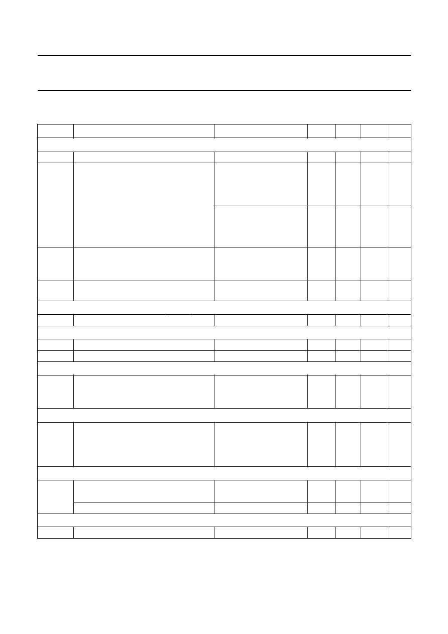
Fig.30 Typical LOW level output sink current as a
function of the supply voltage.
Port P0; V
O
= 1.2 V.
(1) T
amb
=
-
20
∞
C.
(2) T
amb
= 25
∞
C.
(3) T
amb
= 80
∞
C.
handbook, halfpage
0
2
4
6
40
4
16
28
34
10
22
MLC004
IOL
(mA)
V (V)
DD
(3)
(2)
(1)
handbook, halfpage
0
2
4
6
10
0
8
MLB999
6
4
2
IOL
(mA)
V (V)
DD
(3)
(2)
(1)
Fig.31 Typical LOW level output sink current as a
function of the supply voltage.
Ports P1, DP0 and DP1; V
O
= 0.4 V.
(1) T
amb
=
-
20
∞
C.
(2) T
amb
= 25
∞
C.
(3) T
amb
= 80
∞
C.
handbook, halfpage
0
2
4
6
10
0
8
MLC002
6
4
2
IOL
(mA)
V (V)
DD
(3)
(2)
(1)
Outputs VOW1, VOW2, VOW3 and VOB; V
O
= 0.4 V.
(1) T
amb
=
-
20
∞
C.
(2) T
amb
= 25
∞
C.
(3) T
amb
= 80
∞
C.
Fig.32 Typical LOW level output sink current as a
function of the supply voltage.
handbook, halfpage
0
2
4
6
200
0
160
MLC001
120
80
40
IOH
(mA)
V (V)
DD
(3)
(2)
(1)
Fig.33 Typical HIGH level pull-up output source
current as a function of the supply voltage.
Ports P0, P1, DP0 and DP1; V
O
= V
SS
.
(1) T
amb
=
-
20
∞
C.
(2) T
amb
= 25
∞
C.
(3) T
amb
= 80
∞
C.
1996 Nov 29
37
Philips Semiconductors
Product specification
8-bit microcontrollers with OSD and VST
84C44X; 84C64X; 84C84X
handbook, halfpage
0
2
4
6
MLC005
V (V)
DD
(3)
(2)
(1)
200
0
160
120
80
40
IOH
(mA)
Ports P0, P1, DP0 and DP1; V
O
= 0.7V
DD
.
(1) T
amb
=
-
20
∞
C.
(2) T
amb
= 25
∞
C.
(3) T
amb
= 80
∞
C.
Fig.34 Typical HIGH level pull-up output source
current as a function of the supply voltage.
handbook, halfpage
0
2
4
6
5
4
2
1
0
3
MLC003
IOH
(mA)
V (V)
DD
(3)
(2)
(1)
Fig.35 Typical HIGH level pull-up output source
current as a function of the supply voltage.
Outputs VOW1, VOW2, VOW3 and VOB; V
O
= V
DD
-
0.4 V.
(1) T
amb
=
-
20
∞
C.
(2) T
amb
= 25
∞
C.
(3) T
amb
= 80
∞
C.
1996 Nov 29
38
Philips Semiconductors
Product specification
8-bit microcontrollers with OSD and VST
84C44X; 84C64X; 84C84X
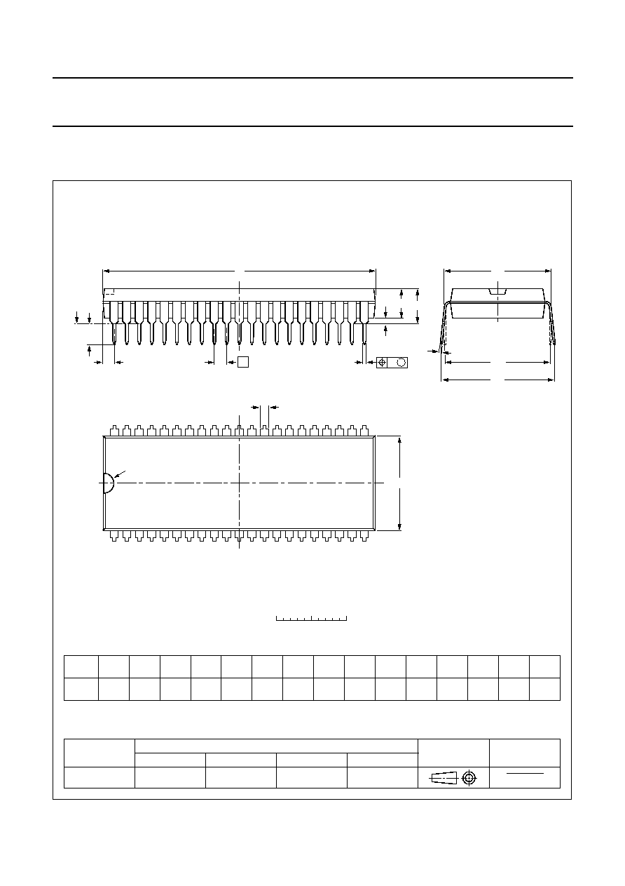
18 PACKAGE OUTLINE
UNIT
b
1
c
E
e
M
H
L
REFERENCES
OUTLINE
VERSION
EUROPEAN
PROJECTION
ISSUE DATE
IEC
JEDEC
EIAJ
mm
DIMENSIONS (mm are the original dimensions)
SOT270-1
90-02-13
95-02-04
b
max.
w
M
E
e
1
1.3
0.8
0.53
0.40
0.32
0.23
38.9
38.4
14.0
13.7
3.2
2.9
0.18
1.778
15.24
15.80
15.24
17.15
15.90
1.73
5.08
0.51
4.0
M
H
c
(e )
1
M
E
A
L
seating plane
A
1
w
M
b
1
e
D
A
2
Z
42
1
22
21
b
E
pin 1 index
0
5
10 mm
scale
Note
1. Plastic or metal protrusions of 0.25 mm maximum per side are not included.
(1)
(1)
D
(1)
Z
A
max.
1
2
A
min.
A
max.
SDIP42: plastic shrink dual in-line package; 42 leads (600 mil)
SOT270-1
1996 Nov 29
39
Philips Semiconductors
Product specification
8-bit microcontrollers with OSD and VST
84C44X; 84C64X; 84C84X
19 SOLDERING
19.1
Introduction
There is no soldering method that is ideal for all IC
packages. Wave soldering is often preferred when
through-hole and surface mounted components are mixed
on one printed-circuit board. However, wave soldering is
not always suitable for surface mounted ICs, or for
printed-circuits with high population densities. In these
situations reflow soldering is often used.
This text gives a very brief insight to a complex technology.
A more in-depth account of soldering ICs can be found in
our
"IC Package Databook" (order code 9398 652 90011).
19.2
Soldering by dipping or by wave
The maximum permissible temperature of the solder is
260
∞
C; solder at this temperature must not be in contact
with the joint for more than 5 seconds.
The total contact time of successive solder waves must not
exceed 5 seconds.
The device may be mounted up to the seating plane, but
the temperature of the plastic body must not exceed the
specified maximum storage temperature (T
stg max
). If the
printed-circuit board has been pre-heated, forced cooling
may be necessary immediately after soldering to keep the
temperature within the permissible limit.
19.3
Repairing soldered joints
Apply a low voltage soldering iron (less than 24 V) to the
lead(s) of the package, below the seating plane or not
more than 2 mm above it. If the temperature of the
soldering iron bit is less than 300
∞
C it may remain in
contact for up to 10 seconds. If the bit temperature is
between 300 and 400
∞
C, contact may be up to 5 seconds.
20 DEFINITIONS
21 LIFE SUPPORT APPLICATIONS
These products are not designed for use in life support appliances, devices, or systems where malfunction of these
products can reasonably be expected to result in personal injury. Philips customers using or selling these products for
use in such applications do so at their own risk and agree to fully indemnify Philips for any damages resulting from such
improper use or sale.
22 PURCHASE OF PHILIPS I
2
C COMPONENTS
Data sheet status
Objective specification
This data sheet contains target or goal specifications for product development.
Preliminary specification
This data sheet contains preliminary data; supplementary data may be published later.
Product specification
This data sheet contains final product specifications.
Limiting values
Limiting values given are in accordance with the Absolute Maximum Rating System (IEC 134). Stress above one or
more of the limiting values may cause permanent damage to the device. These are stress ratings only and operation
of the device at these or at any other conditions above those given in the Characteristics sections of the specification
is not implied. Exposure to limiting values for extended periods may affect device reliability.
Application information
Where application information is given, it is advisory and does not form part of the specification.
Purchase of Philips I
2
C components conveys a license under the Philips' I
2
C patent to use the
components in the I
2
C system provided the system conforms to the I
2
C specification defined by
Philips. This specification can be ordered using the code 9398 393 40011.

Internet: http://www.semiconductors.philips.com
Philips Semiconductors ≠ a worldwide company
© Philips Electronics N.V. 1996
SCA52
All rights are reserved. Reproduction in whole or in part is prohibited without the prior written consent of the copyright owner.
The information presented in this document does not form part of any quotation or contract, is believed to be accurate and reliable and may be changed
without notice. No liability will be accepted by the publisher for any consequence of its use. Publication thereof does not convey nor imply any license
under patent- or other industrial or intellectual property rights.
Netherlands: Postbus 90050, 5600 PB EINDHOVEN, Bldg. VB,
Tel. +31 40 27 82785, Fax. +31 40 27 88399
New Zealand: 2 Wagener Place, C.P.O. Box 1041, AUCKLAND,
Tel. +64 9 849 4160, Fax. +64 9 849 7811
Norway: Box 1, Manglerud 0612, OSLO,
Tel. +47 22 74 8000, Fax. +47 22 74 8341
Philippines: Philips Semiconductors Philippines Inc.,
106 Valero St. Salcedo Village, P.O. Box 2108 MCC, MAKATI,
Metro MANILA, Tel. +63 2 816 6380, Fax. +63 2 817 3474
Poland: Ul. Lukiska 10, PL 04-123 WARSZAWA,
Tel. +48 22 612 2831, Fax. +48 22 612 2327
Portugal: see Spain
Romania: see Italy
Russia: Philips Russia, Ul. Usatcheva 35A, 119048 MOSCOW,
Tel. +7 095 247 9145, Fax. +7 095 247 9144
Singapore: Lorong 1, Toa Payoh, SINGAPORE 1231,
Tel. +65 350 2538, Fax. +65 251 6500
Slovakia: see Austria
Slovenia: see Italy
South Africa: S.A. PHILIPS Pty Ltd., 195-215 Main Road Martindale,
2092 JOHANNESBURG, P.O. Box 7430 Johannesburg 2000,
Tel. +27 11 470 5911, Fax. +27 11 470 5494
South America: Rua do Rocio 220, 5th floor, Suite 51,
04552-903 S„o Paulo, S√O PAULO - SP, Brazil,
Tel. +55 11 821 2333, Fax. +55 11 829 1849
Spain: Balmes 22, 08007 BARCELONA,
Tel. +34 3 301 6312, Fax. +34 3 301 4107
Sweden: Kottbygatan 7, Akalla, S-16485 STOCKHOLM,
Tel. +46 8 632 2000, Fax. +46 8 632 2745
Switzerland: Allmendstrasse 140, CH-8027 ZÐRICH,
Tel. +41 1 488 2686, Fax. +41 1 481 7730
Taiwan: PHILIPS TAIWAN Ltd., 23-30F, 66,
Chung Hsiao West Road, Sec. 1, P.O. Box 22978,
TAIPEI 100, Tel. +886 2 382 4443, Fax. +886 2 382 4444
Thailand: PHILIPS ELECTRONICS (THAILAND) Ltd.,
209/2 Sanpavuth-Bangna Road Prakanong, BANGKOK 10260,
Tel. +66 2 745 4090, Fax. +66 2 398 0793
Turkey: Talatpasa Cad. No. 5, 80640 GÐLTEPE/ISTANBUL,
Tel. +90 212 279 2770, Fax. +90 212 282 6707
Ukraine: PHILIPS UKRAINE, 4 Patrice Lumumba str., Building B, Floor 7,
252042 KIEV, Tel. +380 44 264 2776, Fax. +380 44 268 0461
United Kingdom: Philips Semiconductors Ltd., 276 Bath Road, Hayes,
MIDDLESEX UB3 5BX, Tel. +44 181 730 5000, Fax. +44 181 754 8421
United States: 811 East Arques Avenue, SUNNYVALE, CA 94088-3409,
Tel. +1 800 234 7381
Uruguay: see South America
Vietnam: see Singapore
Yugoslavia: PHILIPS, Trg N. Pasica 5/v, 11000 BEOGRAD,
Tel. +381 11 625 344, Fax.+381 11 635 777
For all other countries apply to: Philips Semiconductors, Marketing & Sales Communications,
Building BE-p, P.O. Box 218, 5600 MD EINDHOVEN, The Netherlands, Fax. +31 40 27 24825
Argentina: see South America
Australia: 34 Waterloo Road, NORTH RYDE, NSW 2113,
Tel. +61 2 9805 4455, Fax. +61 2 9805 4466
Austria: Computerstr. 6, A-1101 WIEN, P.O. Box 213,
Tel. +43 1 60 101, Fax. +43 1 60 101 1210
Belarus: Hotel Minsk Business Center, Bld. 3, r. 1211, Volodarski Str. 6,
220050 MINSK, Tel. +375 172 200 733, Fax. +375 172 200 773
Belgium: see The Netherlands
Brazil: see South America
Bulgaria: Philips Bulgaria Ltd., Energoproject, 15th floor,
51 James Bourchier Blvd., 1407 SOFIA,
Tel. +359 2 689 211, Fax. +359 2 689 102
Canada: PHILIPS SEMICONDUCTORS/COMPONENTS,
Tel. +1 800 234 7381
China/Hong Kong: 501 Hong Kong Industrial Technology Centre,
72 Tat Chee Avenue, Kowloon Tong, HONG KONG,
Tel. +852 2319 7888, Fax. +852 2319 7700
Colombia: see South America
Czech Republic: see Austria
Denmark: Prags Boulevard 80, PB 1919, DK-2300 COPENHAGEN S,
Tel. +45 32 88 2636, Fax. +45 31 57 1949
Finland: Sinikalliontie 3, FIN-02630 ESPOO,
Tel. +358 9 615800, Fax. +358 9 61580/xxx
France: 4 Rue du Port-aux-Vins, BP317, 92156 SURESNES Cedex,
Tel. +33 1 40 99 6161, Fax. +33 1 40 99 6427
Germany: Hammerbrookstraþe 69, D-20097 HAMBURG,
Tel. +49 40 23 53 60, Fax. +49 40 23 536 300
Greece: No. 15, 25th March Street, GR 17778 TAVROS/ATHENS,
Tel. +30 1 4894 339/239, Fax. +30 1 4814 240
Hungary: see Austria
India: Philips INDIA Ltd, Shivsagar Estate, A Block, Dr. Annie Besant Rd.
Worli, MUMBAI 400 018, Tel. +91 22 4938 541, Fax. +91 22 4938 722
Indonesia: see Singapore
Ireland: Newstead, Clonskeagh, DUBLIN 14,
Tel. +353 1 7640 000, Fax. +353 1 7640 200
Israel: RAPAC Electronics, 7 Kehilat Saloniki St, TEL AVIV 61180,
Tel. +972 3 645 0444, Fax. +972 3 649 1007
Italy: PHILIPS SEMICONDUCTORS, Piazza IV Novembre 3,
20124 MILANO, Tel. +39 2 6752 2531, Fax. +39 2 6752 2557
Japan: Philips Bldg 13-37, Kohnan 2-chome, Minato-ku, TOKYO 108,
Tel. +81 3 3740 5130, Fax. +81 3 3740 5077
Korea: Philips House, 260-199 Itaewon-dong, Yongsan-ku, SEOUL,
Tel. +82 2 709 1412, Fax. +82 2 709 1415
Malaysia: No. 76 Jalan Universiti, 46200 PETALING JAYA, SELANGOR,
Tel. +60 3 750 5214, Fax. +60 3 757 4880
Mexico: 5900 Gateway East, Suite 200, EL PASO, TEXAS 79905,
Tel. +9-5 800 234 7381
Middle East: see Italy
Printed in The Netherlands
457021/1200/03/pp40
Date of release: 1996 Nov 29
Document order number:
9397 750 01542