
October 1994
2
Philips Semiconductors
Product specification
8-bit microcontrollers with OSD and VST
84C44X; 84C64X; 84C84X
CONTENTS
1
FEATURES
1.1
PCF84CXXXA kernel
1.2
Derivative features PCA84C640
2
GENERAL DESCRIPTION
2.1
Important
3
ORDERING INFORMATION
4
BLOCK DIAGRAM
5
PINNING INFORMATION
6
DIFFERENCES
7
RESET
7.1
Power-on-reset
8
ANALOG CONTROL
8.1
6-bit PWM DACs
8.1.1
Pin selection for PWM outputs
8.1.2
Polarity of the PWM outputs
8.1.3
Analog output voltage
9
VST CONTROL
9.1
14-bit PWM DAC
9.1.1
14-bit counter
9.1.2
Data and interface latches
9.2
Coarse adjustment
9.3
Fine adjustment
10
AFC INPUT
11
INPUT/OUTPUT ( I/O)
12
ON SCREEN DISPLAY
12.1
Features
12.2
Horizontal display position control
12.3
Vertical display position control
12.4
Clock generator
12.4.1
RC oscillator
12.4.2
LC oscillator
12.5
Display data registers
12.6
Display control registers
12.6.1
Derivative register OSDCA
12.6.2
Derivative registers LINE 0A and LINE 0B
12.6.3
Derivative registers LINE 1A and LINE 1B
12.6.4
Derivative register OSDCB
12.7
OSD display position
12.7.1
Vertical position
12.7.2
Horizontal position
12.8
OSD character size and colour selection
12.8.1
Character size
12.8.2
Colour selection
12.9
Character ROM
13
EMULATION MODE
14
REGISTER MAP
15
LIMITING VALUES
16
DC CHARACTERISTICS
17
AC CHARACTERISTICS
17.1
Characteristic curves
18
PACKAGE OUTLINE
19
SOLDERING
19.1
Plastic dual in-line packages
19.1.1
By dip or wave
19.1.2
Repairing soldered joints
20
DEFINITIONS
21
LIFE SUPPORT APPLICATIONS
22
PURCHASE OF PHILIPS I
2
C COMPONENTS

October 1994
3
Philips Semiconductors
Product specification
8-bit microcontrollers with OSD and VST
84C44X; 84C64X; 84C84X
1
FEATURES
1.1
PCF84CXXXA kernel
�
8-bit CPU, ROM, RAM, I/O in a single 42 leads shrink
DIL package
�
Over 80 instructions all of 1 or 2 cycles
�
29 quasi bidirectional standard I/O port lines
�
Configuration of I/O lines individually selected by mask
�
External interrupt INT/T0
�
2 direct testable inputs T0, T1
�
8-bit programmable timer/event counter
�
3 single level vectored interrupts (external,
timer/counter, I
2
C-bus)
�
Power-on-reset and low voltage detector
�
Single power supply
�
2 power reduction modes: Idle and Stop
�
Operating temperature range:
-
20 to +70
�
C
�
Silicon gate CMOS fabrication process (SAC2).
1.2
Derivative features PCA84C640
Although the PCA84C640 is specifically referred to
throughout this data sheet, the information applies to all
the devices. The small differences between the 84C640
and the other devices are specified in the text and also
highlighted in Chapter 6.
The PCA84C640 comprises:
�
The PCF84CXXXA processor core
�
6 kbytes mask-programmable program ROM
�
128 bytes RAM
�
Multi-master I
2
C-bus interface
�
AFC input for Voltage Synthesized Tuning
(VST; with 3-bit DAC and comparator)
�
On Screen Display (OSD) facility for two rows of
16-characters
�
On Screen Display character set of 64 types
�
Four programmable display dot sizes
�
Half dot character rounding
�
Seven colours for each character
�
One 14-bit PWM output for VST
�
Five 6-bit PWM outputs for analog controls
�
Eight port lines with 10 mA LED drive capability
�
18 general purpose bidirectional I/O lines
plus 11 function-combined I/O lines
�
2 direct testable lines
�
Programmable VSYNCN and HSYNCN input polarity
�
RC oscillator for OSD function.
2
GENERAL DESCRIPTION
The 84C44X; 84C64X; 84C84X denotes the types:
�
PCA84C440; 84C441; 84C443; 84C444
�
PCA84C640; 84C641; 84C643; 84C644
�
PCA84C840; 84C841; 84C843; 84C844,
which are 8-bit microcontrollers with On Screen Display
(OSD) and Voltage Synthesized Tuning (VST) functions.
All are members of the 84CXXX microcontroller family.
There are two oscillator types for the OSD function in the
various types, i.e.,
�
RC oscillator: PCA84C440; 84C443; 84C640; 84C643;
84C840; 84C843
�
LC oscillator: PCA84C441; 84C444; 84C641; 84C644;
84C841; 84C844.
2.1
Important note
This data sheet details the specific properties of the
PCA84C44X, PCA84C64X and PCA84C84X.
The shared characteristics of the PCA84CXXX family of
microcontrollers are described in the PCF84CXXXA
Family single-chip 8-bit Microcontroller of
"Data Handbook
IC14", which should be read in conjunction with this data
sheet.
3
ORDERING INFORMATION
TYPE NUMBER
PACKAGE
TEMPERATURE
RANGE (
�
C)
NAME
DESCRIPTION
VERSION
PCA84C440; 84C443; 84C640; 84C643;
84C840; 84C843
SDIP42
plastic shrink dual in-line
package; 42 leads (600 mil)
SOT270-1
-
20 to +70
PCA84C441; 84C444; 84C641; 84C644;
84C841; 84C844

October 1994
4
Philips Semiconductors
Product specification
8-bit microcontrollers with OSD and VST
84C44X; 84C64X; 84C84X
4
BLOCK DIAGRAM
Fig.1 Block diagram.
handbook, full pagewidth
84CXXX
core
excluding
ROM / RAM
8-bit internal bus
8-BIT
TIMER /
EVENT
COUNTER
CPU
PARALLEL
I / O
PORTS
ROM
(1)
RAM
(2)
8-BIT
I / O
PORTS
6-BIT
DAC
14-BIT
DAC
3-BIT DAC +
COMPARATOR
I C
INTERFACE
2
DISPLAY ON SCREEN
5
P0
P1
DP0
DP1
1 2 3 4 5
VOB
VOW1
VOW2
VOW3
DOSC1
DOSC2
(3)
VSYNCN
HSYNCN
TEST / EMU
XTAL1 (IN)
XTAL2 (OUT)
RESET
TDAC
AFC
SDA
SCL
MCD170
T1
INT / T0
PWM
(4)
(5)
(6)
8
8
8
(1) 4K bytes for the PCA84C440; 84C441; 84C443; 84C444.
6K bytes for the PCA84C640; 84C641; 84C643; 84C644.
8K bytes for the PCA84C840; 84C841; 84C843; 84C844.
(2) 128 bytes for the PCA84C440; 84C441; 84C443; 84C444; 84C640; 84C641; 84C643; 84C644.
192 bytes for the PCA84C840; 84C841; 84C843; 84C844.
(3) For use with an LC oscillator, only available with the:
PCA84C441; 84C444; 84C641; 84C644; 84C841; 84C844.
(4) I
2
C-bus interface not available with the:
PCA84C443; 84C444; 84C643; 84C644; 84C843; 84C844.
(5) DP1.4 only available for PCA84C440; 84C443; 84C640; 84C643; 84C840; 84C843.
(6) T1 = pin 29 for PCA84C440; 84C443; 84C640; 84C643; 84C840; 84C843.
T1 = pin 34 for PCA84C441; 84C444; 84C641; 84C644; 84C841; 84C844.
October 1994
5
Philips Semiconductors
Product specification
8-bit microcontrollers with OSD and VST
84C44X; 84C64X; 84C84X
5
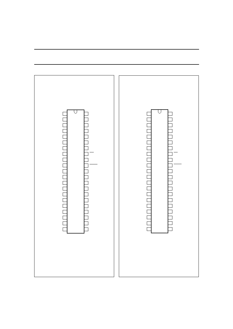
PINNING INFORMATION
Fig.2 Pinning diagram for PCA84CX40; 84CX43.
handbook, halfpage
MCD172
1
2
3
4
5
6
7
8
9
10
11
12
13
40
39
38
37
36
35
34
33
32
31
30
29
28
27
14
15
16
17
18
19
20
22
23
24
25
26
21
42
41
DP0.5/PWM5
DP0.4/PWM4
DP0.3/PWM3
DP0.2/PWM2
DP0.1/PWM1
DP0.0/TDAC
DP1.7/AFC
P1.0
P1.1
P1.2
P1.3
P1.4
P0.0
P0.1
P0.2
P0.3
P0.4
P0.5
P0.6
P0.7
V
SS
DP1.0
DP0.6/SDA
DP0.7/SCL
DP1.1
DP1.2
DP1.3
INT / T0
DP1.4
XTAL2
XTAL1
TEST/EMU
DOSC1
HSYNCN
VOW2/DP1.5
T1
VSYNCN
VOB
VOW1/DP1.6
VOW3
DD
V
RESET
PCA84C640
PCA84C643
PCA84C840
PCA84C843
PCA84C440
PCA84C443
handbook, halfpage
MCD171
1
2
3
4
5
6
7
8
9
10
11
12
13
40
39
38
37
36
35
34
33
32
31
30
29
28
27
14
15
16
17
18
19
20
22
23
24
25
26
21
42
41
DP0.5/PWM5
DP0.4/PWM4
DP0.3/PWM3
DP0.2/PWM2
DP0.1/PWM1
DP0.0/TDAC
DP1.7/AFC
P1.0
P1.1
P1.2
P1.3
P1.4
P0.0
P0.1
P0.2
P0.3
P0.4
P0.5
P0.6
P0.7
V
SS
PCA84C441
PCA84C444
PCA84C641
PCA84C644
PCA84C841
PCA84C844
DP1.0
DP0.6/SDA
DP0.7/SCL
DP1.1
DP1.2
DP1.3
INT/T0
T1
XTAL2
XTAL1
TEST/EMU
DOSC1
HSYNCN
VOW2/DP1.5
DOSC2
VSYNCN
VOB
VOW1/DP1.6
VOW3
DD
V
RESET
Fig.3 Pinning diagram for PCA84CX41; 84CX44.
October 1994
6
Philips Semiconductors
Product specification
8-bit microcontrollers with OSD and VST
84C44X; 84C64X; 84C84X
T
able 1
Pin description
Note
1.
84CX40; 84CX43
denotes the types: PCA84C440, PCA84C443, PCA84C640, PCA84C643, PCA84C840 and PCA84C843.
84CX41; 84CX44
denotes the types: PCA84C441, PCA84C444, PCA84C641, PCA84C644, PCA84C841 and PCA84C844.
SYMBOL
(1)
PIN
(1)
DESCRIPTION
84CX40; 84CX43
84CX41; 84CX44
84CX40; 84CX43
84CX
41; 84CX44
Deviating pinning
DP1.0 to DP1.4
DP1.0 to DP1.3
41, 38, 37, 36, 34
41, 38, 37, 36
Derivative Port 1: quasi-bidirectional I/O lines.
T1
T1
29
34
Direct testable pin and event counter input.
DOSC1
-
28
-
Connection to RC oscillator of OSD clock.
-
DOSC1/DOSC2
-
28, 29
Connections to LC oscillator of OSD clock.
Mutual pinning
DP0.0/TDAC
1
Derivative Port 0: quasi-bidirectional I/O line or 14-bit DAC PWM.
DP0.1 to DP0.5/PWM1 to PWM5
2 to 6
Derivative Port 1: quasi-bidirectional I/O lines or 6-bit DAC PWM.
P1.0 to P1.4
7, 8, 10, 12
Port 1: quasi-bidirectional I/O lines.
P0.0 to P0.7
13 to 20
Port 0: quasi-bidirectional I/O port.
DP1.7/AFC
9
Derivative Port 1:
quasi-bidirectional I/O line or comparator input with 3-bit DAC.
DP0.6/SDA
40
Derivative open drain I/O port or I
2
C-bus data line.
DP0.7/SCL
39
Derivative open drain I/O port or I
2
C- bus clock line.
INT
/T0
35
External interrupt or direct testable line.
DP1.5 to DP1.6/VOW2 to VOW1
23, 22
Derivative Port 1:
quasi-bidirectional I/O lines or character video output.
RESET
33
Initialize input, active LOW
.
XT
AL2, XT
AL1
32, 31
Oscillator output or input terminal for system clock.
TEST/EMU
30
Control input for testing and emulation mode. Ground for normal
operation.
VSYNCN
27
V
ertical synchronous signal input.
HSYNCN
26
Horizontal synchronous signal input.
VOB
25
Blanking output.
VOW3
24
Character video output of OSD.
V
SS
21
Ground.
V
DD
42
Power supply
.