 | ÐлекÑÑоннÑй компоненÑ: BZX84-B15 | СкаÑаÑÑ:  PDF PDF  ZIP ZIP |
Äîêóìåíòàöèÿ è îïèñàíèÿ www.docs.chipfind.ru
DATA SHEET
Product specification
Supersedes data of 1999 May 18
2003 Apr 10
DISCRETE SEMICONDUCTORS
BZX84 series
Voltage regulator diodes
book, halfpage
M3D088
2003 Apr 10
2
Philips Semiconductors
Product specification
Voltage regulator diodes
BZX84 series
FEATURES
·
Total power dissipation: max. 250 mW
·
Three tolerance series:
±
1%,
±
2% and approx.
±
5%
·
Working voltage range: nom. 2.4 to 75 V (E24 range)
·
Non-repetitive peak reverse power dissipation:
max. 40 W.
APPLICATIONS
·
General regulation functions.
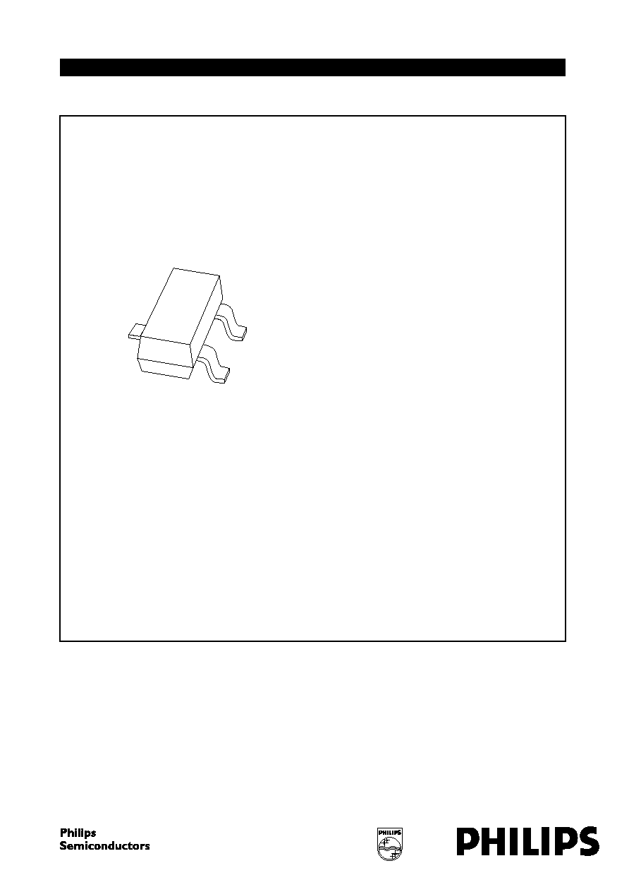
DESCRIPTION
Low-power voltage regulator diodes in small SOT23
plastic SMD packages.
The diodes are available in the normalized E24
±
1%
(BZX84-A),
±
2% (BZX84-B) and approx.
±
5% (BZX84-C)
tolerance range. The series consists of 37 types with
nominal working voltages from 2.4 to 75 V.
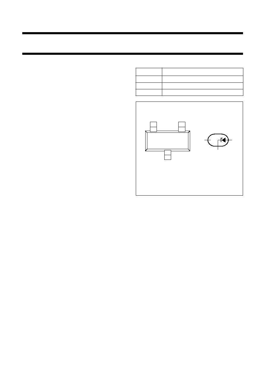
PINNING
PIN
DESCRIPTION
1
anode
2
not connected
3
cathode
Fig.1 Simplified outline (SOT23) and symbol.
handbook, halfpage
MAM243
2
n.c.
1
3
2
1
3
Top view
2003 Apr 10
3
Philips Semiconductors
Product specification
Voltage regulator diodes
BZX84 series
MARKING
Note
1.
= p : Made in Hong Kong.
= t : Made in Malaysia.
= W : Made in China.
TYPE
NUMBER
MARKING
CODE
(1)
TYPE
NUMBER
MARKING
CODE
(1)
TYPE
NUMBER
MARKING
CODE
(1)
TYPE
NUMBER
MARKING
CODE
(1)
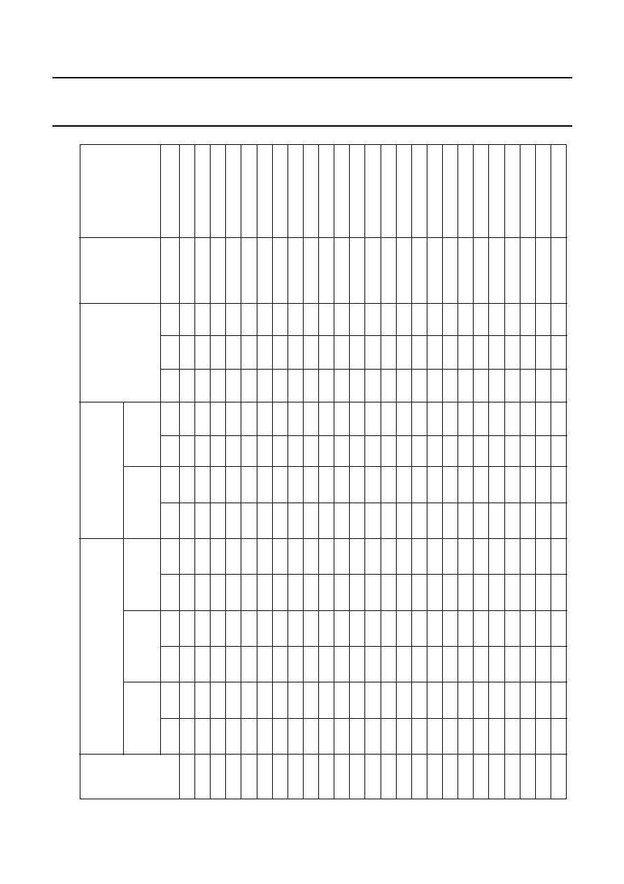
Marking codes for BZX84-A2V4 to BZX84-A75
BZX84-A2V4
Y50 or
50
BZX84-A6V2
Y60 or
60
BZX84-A16
Y70
BZX84-A43
Y80 or
C5
BZX84-A2V7
Y51 or
51
BZX84-A6V8
Y61 or
61
BZX84-A18
Y71
BZX84-A47
Y81
BZX84-A3V0
Y52 or
52
BZX84-A7V5
Y62 or
62
BZX84-A20
Y72 or
C2
BZX84-A51
Y82 or
C6
BZX84-A3V3
Y53
BZX84-A8V2
Y63 or
63
BZX84-A22
Y73
BZX84-A56
Y83
BZX84-A3V6
Y54 or
C1
BZX84-A9V1
Y64 or
64
BZX84-A24
Y74
BZX84-A62
Y84
BZX84-A3V9
Y55 or
55
BZX84-A10
Y65 or
65
BZX84-A27
Y75 or
75
BZX84-A68
Y85
BZX84-A4V3
Y56 or
56
BZX84-A11
Y66 or
04
BZX84-A30
Y76
BZX84-A75
Y86 or
86
BZX84-A4V7
Y57 or
57
BZX84-A12
Y67 or
67
BZX84-A33
Y77
-
-
BZX84-A5V1
Y58 or
58
BZX84-A13
Y68 or
C0
BZX84-A36
Y78 or
C3
-
-
BZX84-A5V6
Y59 or
59
BZX84-A15
Y69 or
69
BZX84-A39
Y79 or
C4
-
-
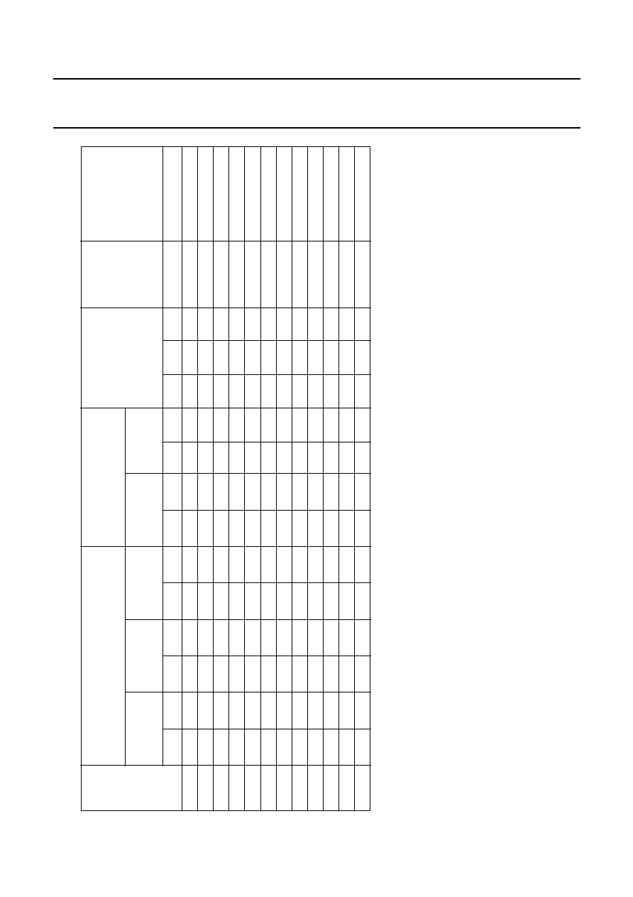
Marking codes for BZX84-B2V4 to BZX84-B75
BZX84-B2V4
Z50 or
Z0
BZX84-B6V2
Z60 or
R5
BZX84-B16
Z70 or
70
BZX84-B43
Z80 or
S5
BZX84-B2V7
Z51 or
Z1
BZX84-B6V8
Z61 or
R6
BZX84-B18
Z71 or
71
BZX84-B47
Z81 or
S6
BZX84-B3V0
Z52 or
S1
BZX84-B7V5
Z62 or
R8
BZX84-B20
Z72 or
72
BZX84-B51
Z82 or
S9
BZX84-B3V3
Z53 or
S2
BZX84-B8V2
Z63 or
R9
BZX84-B22
Z73 or
73
BZX84-B56
Z83 or
R0
BZX84-B3V6
Z54 or
S3
BZX84-B9V1
Z64 or
T1
BZX84-B24
Z74 or
74
BZX84-B62
Z84 or
R3
BZX84-B3V9
Z55 or
S4
BZX84-B10
Z65 or
66
BZX84-B27
Z75 or
Z5
BZX84-B68
Z85 or
R4
BZX84-B4V3
Z56 or
S7
BZX84-B11
Z66 or
Z6
BZX84-B30
Z76 or
Z4
BZX84-B75
Z86 or
R7
BZX84-B4V7
Z57 or
S8
BZX84-B12
Z67 or
Z7
BZX84-B33
Z77 or
Y1
-
-
BZX84-B5V1
Z58 or
R1
BZX84-B13
Z68 or
Z8
BZX84-B36
Z78 or
Y2
-
-
BZX84-B5V6
Z59 or
R2
BZX84-B15
Z69 or
Z9
BZX84-B39
Z79 or
S0
-
-
Marking codes for BZX84-C2V4 to BZX84-C75
BZX84-C2V4
Z11 or
T3
BZX84-C6V2
Z4
BZX84-C16
Y5
BZX84-C43
Y15 or
B4
BZX84-C2V7
Z12 or
T4
BZX84-C6V8
Z5
BZX84-C18
Y6
BZX84-C47
Y16 or
B5
BZX84-C3V0
Z13 or
T9
BZX84-C7V5
Z6
BZX84-C20
Y7
BZX84-C51
Y17 or
B7
BZX84-C3V3
Z14 or
B1
BZX84-C8V2
Z7
BZX84-C22
Y8
BZX84-C56
Y18 or
B8
BZX84-C3V6
Z15 or
B2
BZX84-C9V1
Z8
BZX84-C24
Y9
BZX84-C62
Y19 or
B9
BZX84-C3V9
Z16 or
B3
BZX84-C10
Z9
BZX84-C27
Y10 or
T2
BZX84-C68
Y20 or
B0
BZX84-C4V3
Z17 or
B6
BZX84-C11
Y1
BZX84-C30
Y11 or
T5
BZX84-C75
Y21 or
A1
BZX84-C4V7
Z1
BZX84-C12
Y2
BZX84-C33
Y12 or
T6
-
-
BZX84-C5V1
Z2
BZX84-C13
Y3
BZX84-C36
Y13 or
T7
-
-
BZX84-C5V6
Z3
BZX84-C15
Y4
BZX84-C39
Y14 or
T8
-
-
2003 Apr 10
4
Philips Semiconductors
Product specification
Voltage regulator diodes
BZX84 series
LIMITING VALUES
In accordance with the Absolute Maximum Rating System (IEC 60134).
Note
1. Device mounted on an FR4 printed circuit-board.
ELECTRICAL CHARACTERISTICS
Total BZX84-A and B and C series
T
j
= 25
°
C unless otherwise specified.
SYMBOL
PARAMETER
CONDITIONS
MIN.
MAX.
UNIT
I
F
continuous forward current
-
200
mA
I
ZSM
non-repetitive peak reverse current
t
p
= 100
µ
s; square wave;
T
j
= 25
°
C prior to surge
see Tables
1 and 2
P
tot
total power dissipation
T
amb
= 25
°
C; note 1
-
250
mW
P
ZSM
non-repetitive peak reverse power
dissipation
t
p
= 100
µ
s; square wave;
T
j
= 25
°
C prior to surge; see Fig.2
-
40
W
T
stg
storage temperature
-
65
+150
°
C
T
j
junction temperature
-
65
+150
°
C
SYMBOL
PARAMETER
CONDITIONS
MAX.
UNIT
V
F
forward voltage
I
F
= 10 mA; see Fig.3
0.9
V
I
R
reverse current
BZX84-A/B/C2V4
V
R
= 1 V
50
µ
A
BZX84-A/B/C2V7
V
R
= 1 V
20
µ
A
BZX84-A/B/C3V0
V
R
= 1 V
10
µ
A
BZX84-A/B/C3V3
V
R
= 1 V
5
µ
A
BZX84-A/B/C3V6
V
R
= 1 V
5
µ
A
BZX84-A/B/C3V9
V
R
= 1 V
3
µ
A
BZX84-A/B/C4V3
V
R
= 1 V
3
µ
A
BZX84-A/B/C4V7
V
R
= 2 V
3
µ
A
BZX84-A/B/C5V1
V
R
= 2 V
2
µ
A
BZX84-A/B/C5V6
V
R
= 2 V
1
µ
A
BZX84-A/B/C6V2
V
R
= 4 V
3
µ
A
BZX84-A/B/C6V8
V
R
= 4 V
2
µ
A
BZX84-A/B/C7V5
V
R
= 5 V
1
µ
A
BZX84-A/B/C8V2
V
R
= 5 V
700
nA
BZX84-A/B/C9V1
V
R
= 6 V
500
nA
BZX84-A/B/C10
V
R
= 7 V
200
nA
BZX84-A/B/C11
V
R
= 8 V
100
nA
BZX84-A/B/C12
V
R
= 8 V
100
nA
BZX84-A/B/C13
V
R
= 8 V
100
nA
BZX84-A/B/C15 to 75
V
R
= 0.7V
Znom
50
nA
2003
Apr
10
5
Philips Semiconductors
Product specification
V
oltage regulator diodes
BZX84 ser
ies
This text is here in white to force landscape pages to be rotated correctly when browsing through the pdf in the Acrobat reader.This text is here in
_
white to force landscape pages to be rotated correctly when browsing through the pdf in the Acrobat reader.This text is here inThis text is here in
white to force landscape pages to be rotated correctly when browsing through the pdf in the Acrobat reader. white to force landscape pages to be ...
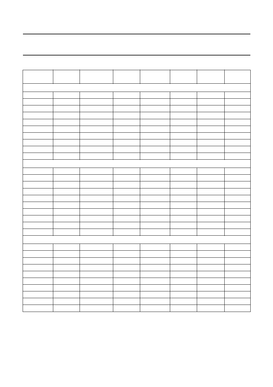
Table 1
Per type BZX84-A/B/C2V4 to A/B/C24
T
j
= 25
°
C unless otherwise specified.
BZX84-
Axxx
Bxxx
Cxxx
WORKING VOLTAGE
V
Z
(V)
at I
Ztest
= 5 mA
DIFFERENTIAL
RESISTANCE
r
dif
(
)
TEMP. COEFF.
S
Z
(mV/K)
at I
Ztest
= 5 mA
(see Figs 4 and 5)
DIODE CAP.
C
d
(pF)
at f = 1 MHz;
V
R
= 0 V
NON-REPETITIVE
PEAK REVERSE
CURRENT
I
ZSM
(A)
at t
p
= 100
µ
s;
T
amb
= 25
°
C
Tol.
±
1% (A)
Tol.
±
2% (B)
Tol. approx.
±
5% (C)
at
I
Ztest
= 1 mA
at
I
Ztest
= 5 mA
MIN.
MAX.
MIN.
MAX.
MIN.
MAX.
TYP.
MAX.
TYP.
MAX.
MIN.
TYP.
MAX.
MAX.
MAX.
2V4
2.37
2.43
2.35
2.45
2.2
2.6
275
600
70
100
-
3.5
-
1.6
0
450
6.0
2V7
2.67
2.73
2.65
2.75
2.5
2.9
300
600
75
100
-
3.5
-
2.0
0
450
6.0
3V0
2.97
3.03
2.94
3.06
2.8
3.2
325
600
80
95
-
3.5
-
2.1
0
450
6.0
3V3
3.26
3.34
3.23
3.37
3.1
3.5
350
600
85
95
-
3.5
-
2.4
0
450
6.0
3V6
3.56
3.64
3.53
3.67
3.4
3.8
375
600
85
90
-
3.5
-
2.4
0
450
6.0
3V9
3.86
3.94
3.82
3.98
3.7
4.1
400
600
85
90
-
3.5
-
2.5
0
450
6.0
4V3
4.25
4.35
4.21
4.39
4.0
4.6
410
600
80
90
-
3.5
-
2.5
0
450
6.0
4V7
4.65
4.75
4.61
4.79
4.4
5.0
425
500
50
80
-
3.5
-
1.4
0.2
300
6.0
5V1
5.04
5.16
5.00
5.20
4.8
5.4
400
480
40
60
-
2.7
-
0.8
1.2
300
6.0
5V6
5.54
5.66
5.49
5.71
5.2
6.0
80
400
15
40
-
2.0
1.2
2.5
300
6.0
6V2
6.13
6.27
6.08
6.32
5.8
6.6
40
150
6
10
0.4
2.3
3.7
200
6.0
6V8
6.73
6.87
6.66
6.94
6.4
7.2
30
80
6
15
1.2
3.0
4.5
200
6.0
7V5
7.42
7.58
7.35
7.65
7.0
7.9
30
80
6
15
2.5
4.0
5.3
150
4.0
8V2
8.11
8.29
8.04
8.36
7.7
8.7
40
80
6
15
3.2
4.6
6.2
150
4.0
9V1
9.00
9.20
8.92
9.28
8.5
9.6
40
100
6
15
3.8
5.5
7.0
150
3.0
10
9.90
10.10
9.80
10.20
9.4
10.6
50
150
8
20
4.5
6.4
8.0
90
3.0
11
10.80
11.11
10.80
11.20
10.4
11.6
50
150
10
20
5.4
7.4
9.0
85
2.5
12
11.88
12.12
11.80
12.20
11.4
12.7
50
150
10
25
6.0
8.4
10.0
85
2.5
13
12.87
13.13
12.70
13.30
12.4
14.1
50
170
10
30
7.0
9.4
11.0
80
2.5
15
14.85
15.15
14.70
15.30
13.8
15.6
50
200
10
30
9.2
11.4
13.0
75
2.0
16
15.84
16.16
15.70
16.30
15.3
17.1
50
200
10
40
10.4
12.4
14.0
75
1.5
18
17.82
18.18
17.60
18.40
16.8
19.1
50
225
10
45
12.4
14.4
16.0
70
1.5
20
19.80
20.20
19.60
20.40
18.8
21.2
60
225
15
55
14.4
16.4
18.0
60
1.5
22
21.78
22.22
21.60
22.40
20.8
23.3
60
250
20
55
16.4
18.4
20.0
60
1.25
24
23.76
24.24
23.50
24.50
22.8
25.6
60
250
25
70
18.4
20.4
22.0
55
1.25
2003
Apr
10
6
Philips Semiconductors
Product specification
V
oltage regulator diodes
BZX84 ser
ies
This text is here in white to force landscape pages to be rotated correctly when browsing through the pdf in the Acrobat reader.This text is here in
_
white to force landscape pages to be rotated correctly when browsing through the pdf in the Acrobat reader.This text is here inThis text is here in
white to force landscape pages to be rotated correctly when browsing through the pdf in the Acrobat reader. white to force landscape pages to be ...
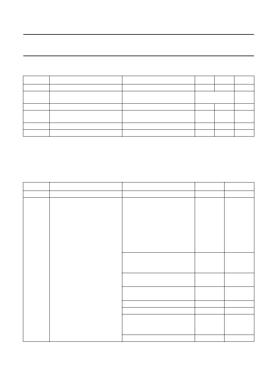
Table 2
Per type BZX84-A/B/C27 to A/B/C75
T
j
= 25
°
C unless otherwise specified.
BZX84-
Axxx
Bxxx
Cxxx
WORKING VOLTAGE
V
Z
(V)
at I
Ztest
= 2 mA
DIFFERENTIAL
RESISTANCE
r
dif
(
)
TEMP. COEFF.
S
Z
(mV/K)
at I
Ztest
= 2 mA
(see Figs 4 and 5)
DIODE CAP.
C
d
(pF)
at f = 1 MHz;
V
R
= 0 V
NON-REPETITIVE
PEAK REVERSE
CURRENT
I
ZSM
(A)
at t
p
= 100
µ
s;
T
amb
= 25
°
C
Tol.
±
1% (A)
Tol.
±
2% (B)
Tol. approx.
±
5% (C)
at
I
Ztest
= 0.5 mA
at
I
Ztest
= 2 mA
MIN.
MAX.
MIN.
MAX.
MIN.
MAX.
TYP.
MAX.
TYP.
MAX.
MIN.
TYP.
MAX.
MAX.
MAX.
27
26.73
27.27
26.50
27.50
25.1
28.9
65
300
25
80
21.4
23.4
25.3
50
1.0
30
29.70
30.30
29.40
30.60
28.0
32.0
70
300
30
80
24.4
26.6
29.4
50
1.0
33
32.67
33.33
32.30
33.70
31.0
35.0
75
325
35
80
27.4
29.7
33.4
45
0.9
36
35.64
36.36
35.30
36.70
34.0
38.0
80
350
35
90
30.4
33.0
37.4
45
0.8
39
38.61
39.39
38.20
39.80
37.0
41.0
80
350
40
130
33.4
36.4
41.2
45
0.7
43
42.57
43.43
42.10
43.90
40.0
46.0
85
375
45
150
37.6
41.2
46.6
40
0.6
47
46.53
47.47
46.10
47.90
44.0
50.0
85
375
50
170
42.0
46.1
51.8
40
0.5
51
50.49
51.51
50.00
52.00
48.0
54.0
90
400
60
180
46.6
51.0
57.2
40
0.4
56
55.44
56.56
54.90
57.10
52.0
60.0
100
425
70
200
52.2
57.0
63.8
40
0.3
62
61.38
62.62
60.80
63.20
58.0
66.0
120
450
80
215
58.8
64.4
71.6
35
0.3
68
67.32
68.68
66.60
69.40
64.0
72.0
150
475
90
240
65.6
71.7
79.8
35
0.25
75
74.25
75.75
73.50
76.50
70.0
79.0
170
500
95
255
73.4
80.2
88.6
35
0.2

2003 Apr 10
7
Philips Semiconductors
Product specification
Voltage regulator diodes
BZX84 series
THERMAL CHARACTERISTICS
Note
1. Device mounted on an FR4 printed circuit-board.
SYMBOL
PARAMETER
CONDITIONS
VALUE
UNIT
R
th j-tp
thermal resistance from junction to tie-point
330
K/W
R
th j-a
thermal resistance from junction to ambient
note 1
500
K/W
2003 Apr 10
8
Philips Semiconductors
Product specification
Voltage regulator diodes
BZX84 series
GRAPHICAL DATA
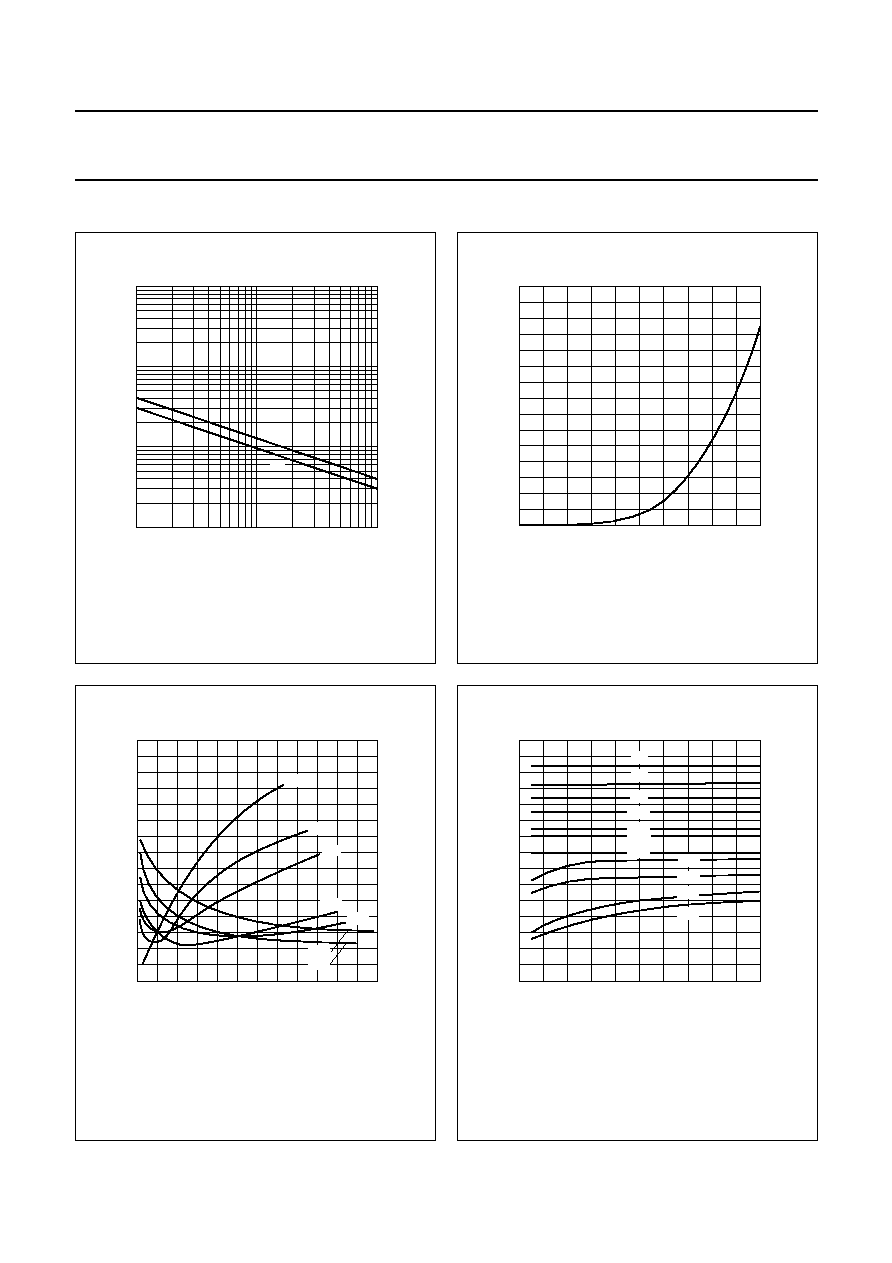
Fig.2
Maximum permissible non-repetitive peak
reverse power dissipation versus duration.
handbook, halfpage
MBG801
10
3
1
duration (ms)
PZSM
(W)
10
10
2
10
-
1
10
1
(1)
(2)
(1) T
j
= 25
°
C (prior to surge).
(2) T
j
= 150
°
C (prior to surge).
Fig.3
Forward current as a function of forward
voltage; typical values.
handbook, halfpage
0.6
1
300
100
0
200
MBG781
0.8
VF (V)
IF
(mA)
T
j
= 25
°
C.
Fig.4
Temperature coefficient as a function of
working current; typical values.
handbook, halfpage
0
60
0
-
2
-
3
-
1
MBG783
20
40
IZ (mA)
SZ
(mV/K)
4V3
3V9
3V6
3V0
2V4
2V7
3V3
BZX84-A/B/C2V4 to A/B/C4V3.
T
j
= 25 to 150
°
C.
Fig.5
Temperature coefficient as a function of
working current; typical values.
handbook, halfpage
0
20
16
10
0
-
5
5
MBG782
4
8
12
IZ (mA)
SZ
(mV/K)
4V7
12
11
10
9V1
8V2
7V5
6V8
6V2
5V6
5V1
BZX84-A/B/C4V7 to A/B/C12.
T
j
= 25 to 150
°
C.
2003 Apr 10
9
Philips Semiconductors
Product specification
Voltage regulator diodes
BZX84 series
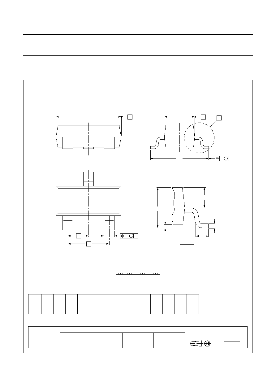
PACKAGE OUTLINE
UNIT
A
1
max.
b
p
c
D
E
e
1
H
E
L
p
Q
w
v
REFERENCES
OUTLINE
VERSION
EUROPEAN
PROJECTION
ISSUE DATE
97-02-28
99-09-13
IEC
JEDEC
EIAJ
mm
0.1
0.48
0.38
0.15
0.09
3.0
2.8
1.4
1.2
0.95
e
1.9
2.5
2.1
0.55
0.45
0.1
0.2
DIMENSIONS (mm are the original dimensions)
0.45
0.15
SOT23
TO-236AB
bp
D
e1
e
A
A1
Lp
Q
detail X
HE
E
w
M
v
M
A
B
A
B
0
1
2 mm
scale
A
1.1
0.9
c
X
1
2
3
Plastic surface mounted package; 3 leads
SOT23

2003 Apr 10
10
Philips Semiconductors
Product specification
Voltage regulator diodes
BZX84 series
DATA SHEET STATUS
Notes
1. Please consult the most recently issued data sheet before initiating or completing a design.
2. The product status of the device(s) described in this data sheet may have changed since this data sheet was
published. The latest information is available on the Internet at URL http://www.semiconductors.philips.com.
3. For data sheets describing multiple type numbers, the highest-level product status determines the data sheet status.
LEVEL
DATA SHEET
STATUS
(1)
PRODUCT
STATUS
(2)(3)
DEFINITION
I
Objective data
Development
This data sheet contains data from the objective specification for product
development. Philips Semiconductors reserves the right to change the
specification in any manner without notice.
II
Preliminary data Qualification
This data sheet contains data from the preliminary specification.
Supplementary data will be published at a later date. Philips
Semiconductors reserves the right to change the specification without
notice, in order to improve the design and supply the best possible
product.
III
Product data
Production
This data sheet contains data from the product specification. Philips
Semiconductors reserves the right to make changes at any time in order
to improve the design, manufacturing and supply. Relevant changes will
be communicated via a Customer Product/Process Change Notification
(CPCN).
DEFINITIONS
Short-form specification
The data in a short-form
specification is extracted from a full data sheet with the
same type number and title. For detailed information see
the relevant data sheet or data handbook.
Limiting values definition
Limiting values given are in
accordance with the Absolute Maximum Rating System
(IEC 60134). Stress above one or more of the limiting
values may cause permanent damage to the device.
These are stress ratings only and operation of the device
at these or at any other conditions above those given in the
Characteristics sections of the specification is not implied.
Exposure to limiting values for extended periods may
affect device reliability.
Application information
Applications that are
described herein for any of these products are for
illustrative purposes only. Philips Semiconductors make
no representation or warranty that such applications will be
suitable for the specified use without further testing or
modification.
DISCLAIMERS
Life support applications
These products are not
designed for use in life support appliances, devices, or
systems where malfunction of these products can
reasonably be expected to result in personal injury. Philips
Semiconductors customers using or selling these products
for use in such applications do so at their own risk and
agree to fully indemnify Philips Semiconductors for any
damages resulting from such application.
Right to make changes
Philips Semiconductors
reserves the right to make changes in the products -
including circuits, standard cells, and/or software -
described or contained herein in order to improve design
and/or performance. When the product is in full production
(status `Production'), relevant changes will be
communicated via a Customer Product/Process Change
Notification (CPCN). Philips Semiconductors assumes no
responsibility or liability for the use of any of these
products, conveys no licence or title under any patent,
copyright, or mask work right to these products, and
makes no representations or warranties that these
products are free from patent, copyright, or mask work
right infringement, unless otherwise specified.

2003 Apr 10
11
Philips Semiconductors
Product specification
Voltage regulator diodes
BZX84 series
NOTES

© Koninklijke Philips Electronics N.V. 2003
SCA75
All rights are reserved. Reproduction in whole or in part is prohibited without the prior written consent of the copyright owner.
The information presented in this document does not form part of any quotation or contract, is believed to be accurate and reliable and may be changed
without notice. No liability will be accepted by the publisher for any consequence of its use. Publication thereof does not convey nor imply any license
under patent- or other industrial or intellectual property rights.
Philips Semiconductors a worldwide company
Contact information
For additional information please visit http://www.semiconductors.philips.com.
Fax: +31 40 27 24825
For sales offices addresses send e-mail to: sales.addresses@www.semiconductors.philips.com.
Printed in The Netherlands
613514/03/pp
12
Date of release:
2003 Apr 10
Document order number:
9397 750 10959
Document Outline
- FEATURES
- APPLICATIONS
- DESCRIPTION
- PINNING
- MARKING
- LIMITING VALUES
- ELECTRICAL CHARACTERISTICS
- THERMAL CHARACTERISTICS
- GRAPHICAL DATA
- PACKAGE OUTLINE
- DATA SHEET STATUS
- DEFINITIONS
- DISCLAIMERS