HSTL16918 9-bit to 18-bit HSTL-to-LVTTL memory address latch

Philips
Semiconductors
HSTL16918
9-bit to 18-bit HSTL-to-LVTTL
memory address latch
Product data
2001 Jun 16
INTEGRATED CIRCUITS

Philips Semiconductors
Product data
HSTL16918
9-bit to 18-bit HSTL-to-LVTTL memory address latch
2
2001 Jun 16
853-2258 26484
FEATURES
·
Inputs meet JEDEC HSTL Std. JESD 86, and outputs meet
Level III specifications
·
ESD classification testing is done to JEDEC Standard JESD22.
Protection exceeds 2000 V to HBM per method A114.
·
Latch-up testing is done to JEDEC Standard JESD78, which
exceeds 100 mA.
·
Packaged in 48-pin plastic thin shrink small outline package
(TSSOP48)
DESCRIPTION
The HSTL16918 is a 9-bit to 18-bit D-type latch designed for
3.15 to 3.45 V V
CC
operation. The D inputs accept HSTL levels and
the Q outputs provide LVTTL levels.
The HSTL16918 is particularly suitable for driving an address bus to
two banks of memory. Each bank of nine outputs is controlled with
its own latch-enable (LE) input.
Each of the nine D inputs is tied to the inputs of two D-type latches
that provide true data (Q) at the outputs. While LE is LOW the Q
outputs of the corresponding nine latches follow the D inputs. When
LE is taken HIGH, the Q outputs are latched at the levels set up at
the D inputs.
The HSTL16918 is characterized for operation from 0 to +70
°
C.
PIN CONFIGURATION
SW00768
1
2
3
4
5
6
7
8
9
10
11
12
13
14
15
16
17
18
19
20
29
30
31
32
33
34
35
36
37
38
39
40
41
42
43
44
45
46
47
48
2Q1
1Q1
GND
D1
D2
V
CC
D3
GND
1LE
GND
V
REF
GND
2LE
GND
D4
D5
D6
D7
V
CC
D8
GND
2Q7
1Q7
V
CC
2Q6
1Q6
GND
2Q5
1Q5
GND
2Q4
1Q4
V
CC
2Q3
1Q3
GND
2Q2
1Q2
V
CC
V
CC
21
22
23
24
25
26
27
28
D9
GND
2Q9
1Q9
V
CC
V
CC
2Q8
1Q8
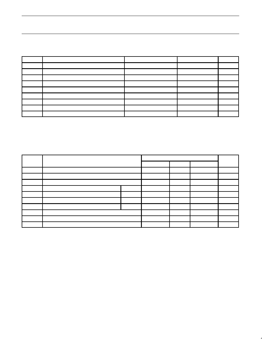
ORDERING INFORMATION
PACKAGES
TEMPERATURE RANGE
ORDER CODE
DWG NUMBER
48-pin plastic thin shrink small outline package
(TSSOP48)
0 to +70
°
C
HSTL16918DGG
SOT362-1

Philips Semiconductors
Product data
HSTL16918
9-bit to 18-bit HSTL-to-LVTTL memory address latch
2001 Jun 16
3
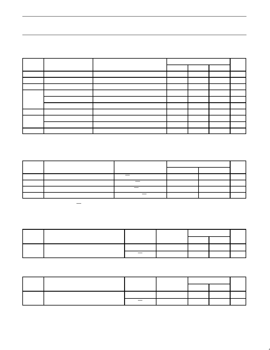
PIN DESCRIPTION
PIN
SYMBOL
FUNCTION
4, 5, 7, 8, 16, 17,
18, 20, 21
D[19]
Inputs
2, 46, 43, 40, 37,
34, 31, 28, 24
1Q[19]
Outputs
1, 45, 42, 39, 36,
33, 30, 27, 23
2Q[19]
Outputs
10
1LE
Latch enable
14
2LE
Latch enable
12
V
REF
Reference voltage
6, 19, 25, 26, 32,
41, 47, 48
V
CC
Supply voltage
3, 9, 11, 13, 15,
22, 29, 35, 38, 44
GND
Ground
LOGIC DIAGRAM (positive logic)
2
10
1LE
4
D1
1Q1
1D
C1
1
14
2LE
2Q1
1D
C1
TO EIGHT OTHER CHANNELS
SW00769
V
REF
12
FUNCTION TABLE
INPUTS
OUTPUT
LE
D
Q
L
H
H
L
L
L
H
X
Q
0
1
NOTE:
1. Output level before the indicated steady-state input conditions
were established.
Philips Semiconductors
Product data
HSTL16918
9-bit to 18-bit HSTL-to-LVTTL memory address latch
2001 Jun 16
4
ABSOLUTE MAXIMUM RATINGS
1
Over operating free-air temperature range (unless otherwise noted).
SYMBOL
PARAMETER
CONDITIONS
RATING
UNIT
V
CC
Supply voltage range
0.5 to +4.6
V
V
I
Input voltage range
2
0.5 to V
CC
+0.5
V
V
O
Output voltage range
2
0.5 to V
CC
+0.5
V
I
IK
Input clamp current
V
I
< 0
50
mA
I
OK
Output clamp current
3
V
O
< 0 or V
O
> V
CC
±
50
mA
I
O
Continuous output current
V
O
= 0 to V
CC
±
50
mA
Continuous current through each V
CC
or GND
±
100
mA
JA
Package thermal impedance
4
89
°
C/W
T
stg
Storage temperature range
65 to +150
°
C
NOTES:
1. Stresses beyond those listed may cause permanent damage to the device. These are stress ratings only and functional operation of the
device at these or any other conditions beyond those indicated under "recommended operating conditions" is not implied. Exposure to
absolute-maximum-rated conditions for extended periods may affect device reliability.
2. The input and output negative-voltage ratings may be exceeded if the input and output clamp-current ratings are observed.
3. This current flows only when the output is in the high state and V
O
> V
CC
.
4. The package thermal impedance is calculated in accordance with JESD 51.
RECOMMENDED OPERATING CONDITIONS
1
SYMBOL
PARAMETER
LIMITS
UNIT
SYMBOL
PARAMETER
Min
Nom
Max
UNIT
V
CC
Supply voltage
3.15
3.45
V
V
REF
Reference voltage
0.68
0.75
0.9
V
V
I
Input voltage
0
1.5
V
V
IH
AC high-level input voltage
All inputs
V
REF
+ 200 mV
V
V
IL
AC low-level input voltage
All inputs
V
REF
200 mV
V
V
IH
DC high-level input voltage
All inputs
V
REF
+ 100 mV
V
V
IL
DC low-level input voltage
All inputs
V
REF
100 mV
V
I
OH
High-level output current
24
mA
I
OL
Low-level output current
24
mA
T
amb
Operating free-air temperature range
0
+70
°
C
NOTE:
1. All unused inputs of the device must be held at V
CC
or GND to ensure proper device operation.
Philips Semiconductors
Product data
HSTL16918
9-bit to 18-bit HSTL-to-LVTTL memory address latch
2001 Jun 16
5
ELECTRICAL CHARACTERISTICS
Over recommended operating free-air temperature range (unless otherwise noted).
SYMBOL
PARAMETER
TEST CONDITIONS
LIMITS
UNIT
SYMBOL
PARAMETER
TEST CONDITIONS
Min
Typ
1
Max
UNIT
V
IK
V
CC
= 3.15 V; I
I
= 18 mA
1.2
V
V
OH
V
CC
= 3.15 V; I
OH
= 24 mA
2.4
V
V
OL
V
CC
= 3.15 V; I
OL
= 24 mA
0.5
V
Control inputs
V
CC
= 3.45 V; V
I
= 0 or 1.5 V
±
5
µ
A
I
I
Data inputs
V
CC
= 3.45 V; V
I
= 0 or 1.5 V
±
5
µ
A
V
REF
V
CC
= 3.45 V; V
REF
= 0.68 V or 0.9 V
90
µ
A
I
CC
V
CC
= 3.45 V; V
I
= 0 or 1.5 V
50
100
mA
C
Control inputs
V
CC
= 0 or 3.3 V; V
I
= 0 or 3.3 V
2
pF
C
I
Data inputs
V
CC
= 0 or 3.3 V; V
I
= 0 or 3.3 V
2.5
pF
C
O
Outputs
V
CC
= 0 V; V
O
= 0 V
4
pF
NOTE:
1. All typical values are at V
CC
= 3.3 V; T
amb
= 25
°
C.
TIMING REQUIREMENTS
Over recommended operating free-air temperature range (unless otherwise noted).
SYMBOL
PARAMETER
TEST CONDITIONS
V
CC
= 3.3 V
±
0.15 V
UNIT
SYMBOL
PARAMETER
TEST CONDITIONS
Min
Max
UNIT
t
w
Pulse duration
LE LOW (Figure 1)
3
ns
t
su
Setup time
D before LE
(Figure 2)
2
ns
t
h
Hold time
D after LE
(Figure 2)
1
ns
t
ldr
Data race condition time
1
D after LE
0
ns
NOTE:
1. This is the maximum time after LE switches LOW that the data input can return to the latched state from the opposite state without producing
a glitch on the output.
SWITCHING CHARACTERISTICS
Over recommended operating free-air temperature range; V
REF
= 0.75 V.
SYMBOL
PARAMETER
FROM
TO
V
CC
= 3.3 V
±
0.15 V
UNIT
SYMBOL
PARAMETER
(INPUT)
(OUTPUT)
Min
Max
UNIT
t
Propagation delay (Figure 3)
D
Q
1.9
3.4
ns
t
pd
Propagation delay (Figure 3)
LE
Q
1.9
4.2
ns
SIMULTANEOUS SWITCHING CHARACTERISTICS
Over recommended operating free-air temperature range; V
REF
= 0.75 V
SYMBOL
PARAMETER
FROM
TO
V
CC
= 3.3 V
±
0.15 V
UNIT
SYMBOL
PARAMETER
(INPUT)
(OUTPUT)
Min
Max
UNIT
t
Propagation delay; all outputs switching
D
Q
1.9
4.4
ns
t
pd
g
y
g
(Figure 3)
LE
Q
1.9
5.2
ns
Philips Semiconductors
Product data
HSTL16918
9-bit to 18-bit HSTL-to-LVTTL memory address latch
2001 Jun 16
6
VOLTAGE WAVEFORMS
1.25 V
0.25 V
INPUT
t
w
V
REF
V
REF
SW00770
Figure 1. Pulse duration
1.25 V
0.25 V
DATA INPUT
V
REF
V
REF
V
REF
LE
t
su
t
h
1.25 V
0.25 V
SW00771
Figure 2. Setup and Hold times
V
REF
V
REF
1.5 V
1.5 V
1.25 V
0.25 V
V
OH
V
OL
t
PHL
t
PLH
INPUT
(Note 1)
OUTPUT
SW00772
Figure 3. Propagation delay times
NOTES:
1. All input pulses are supplied by generators having the following
characteristics: PRR
10 MHz, Z
O
= 50
, t
r
1 ns, t
f
1 ns.
2. The outputs are measured one at a time with one transition per
measurement.
3. t
PHL
and t
PLH
are the same as t
pd
.
LOAD CIRCUIT
C
L
= 80 PF
(see Note)
500
FROM OUTPUT
UNDER TEST
SW00773
NOTE: C
L
includes probe and jig capacitance.
Figure 4. Load circuit

Philips Semiconductors
Product data
HSTL16918
9-bit to 18-bit HSTL-to-LVTTL memory address latch
2001 Jun 16
7
TSSOP48:
plastic thin shrink small outline package; 48 leads; body width 6.1 mm
SOT362-1

Philips Semiconductors
Product data
HSTL16918
9-bit to 18-bit HSTL-to-LVTTL memory address latch
2001 Jun 16
8
Definitions
Short-form specification -- The data in a short-form specification is extracted from a full data sheet with the same type number and title. For
detailed information see the relevant data sheet or data handbook.
Limiting values definition -- Limiting values given are in accordance with the Absolute Maximum Rating System (IEC 134). Stress above one
or more of the limiting values may cause permanent damage to the device. These are stress ratings only and operation of the device at these or
at any other conditions above those given in the Characteristics sections of the specification is not implied. Exposure to limiting values for extended
periods may affect device reliability.
Application information -- Applications that are described herein for any of these products are for illustrative purposes only. Philips
Semiconductors make no representation or warranty that such applications will be suitable for the specified use without further testing or
modification.
Disclaimers
Life support -- These products are not designed for use in life support appliances, devices or systems where malfunction of these products can
reasonably be expected to result in personal injury. Philips Semiconductors customers using or selling these products for use in such applications
do so at their own risk and agree to fully indemnify Philips Semiconductors for any damages resulting from such application.
Right to make changes -- Philips Semiconductors reserves the right to make changes, without notice, in the products, including circuits, standard
cells, and/or software, described or contained herein in order to improve design and/or performance. Philips Semiconductors assumes no
responsibility or liability for the use of any of these products, conveys no license or title under any patent, copyright, or mask work right to these
products, and makes no representations or warranties that these products are free from patent, copyright, or mask work right infringement, unless
otherwise specified.
Philips Semiconductors
811 East Arques Avenue
P.O. Box 3409
Sunnyvale, California 940883409
Telephone 800-234-7381
©
Copyright Philips Electronics North America Corporation 2001
All rights reserved. Printed in U.S.A.
Date of release: 06-01
Document order number:
9397 750 08474
Philips
Semiconductors
Data sheet status
[1]
Objective data
Preliminary data
Product data
Product
status
[2]
Development
Qualification
Production
Definitions
This data sheet contains data from the objective specification for product development.
Philips Semiconductors reserves the right to change the specification in any manner without notice.
This data sheet contains data from the preliminary specification. Supplementary data will be
published at a later date. Philips Semiconductors reserves the right to change the specification
without notice, in order to improve the design and supply the best possible product.
This data sheet contains data from the product specification. Philips Semiconductors reserves the
right to make changes at any time in order to improve the design, manufacturing and supply.
Changes will be communicated according to the Customer Product/Process Change Notification
(CPCN) procedure SNW-SQ-650A.
Data sheet status
[1] Please consult the most recently issued datasheet before initiating or completing a design.
[2] The product status of the device(s) described in this data sheet may have changed since this data sheet was published. The latest information is available on
the Internet at URL http://www.semiconductors.philips.com.
Document Outline
- FEATURES
- PIN CONFIGURATION
- DESCRIPTION
- ORDERING INFORMATION
- PIN DESCRIPTION
- LOGIC DIAGRAM (positive logic)
- FUNCTION TABLE
- ABSOLUTE MAXIMUM RATINGS
- RECOMMENDED OPERATING CONDITIONS 1
- ELECTRICAL CHARACTERISTICS
- TIMING REQUIREMENTS
- SWITCHING CHARACTERISTICS
- SIMULTANEOUS SWITCHING CHARACTERISTICS
- VOLTAGE WAVEFORMS
- LOAD CIRCUIT
- Data sheet status
- Definitions
- Disclaimers