Äîêóìåíòàöèÿ è îïèñàíèÿ www.docs.chipfind.ru

DATA SHEET
Product specification
Supersedes data of 1999 Jan 01
File under Integrated Circuits, IC11
2001 Nov 23
INTEGRATED CIRCUITS
HTRC11001T
HITAG reader chip

2001 Nov 23
2
Philips Semiconductors
Product specification
HITAG reader chip
HTRC11001T
CONTENTS
1
FEATURES
2
APPLICATIONS
3
GENERAL DESCRIPTION
4
QUICK REFERENCE DATA
5
ORDERING INFORMATION
6
BLOCK DIAGRAM
7
PINNING
8
FUNCTIONAL DESCRIPTION
8.1
Power supply
8.2
Antenna drivers
8.3
Diagnosis
8.4
Oscillator with programmable divider
8.5
Adaptive sampling time demodulator
8.6
Idle and Power-down mode
8.7
Serial interface
8.7.1
Communication protocol
8.7.2
Glitch filter
8.8
Commands
8.8.1
Command READ_TAG
8.8.2
Command WRITE_TAG_N
8.8.3
Command WRITE_TAG
8.8.4
Command READ_PHASE
8.8.5
Command SET_SAMPLING_TIME
8.8.6
Command GET_SAMPLING_TIME
8.8.7
Command SET_CONFIG_PAGE
8.8.8
Command GET_CONFIG_PAGE
9
LIMITING VALUES
10
DC CHARACTERISTICS
11
AC CHARACTERISTICS
12
APPLICATION INFORMATION
13
PACKAGE OUTLINE
14
SOLDERING
14.1
Introduction to soldering surface mount
packages
14.2
Reflow soldering
14.3
Wave soldering
14.4
Manual soldering
14.5
Suitability of surface mount IC packages for
wave and reflow soldering methods
15
DATA SHEET STATUS
16
DEFINITIONS
17
DISCLAIMERS
2001 Nov 23
3
Philips Semiconductors
Product specification
HITAG reader chip
HTRC11001T
1
FEATURES
·
Combines all analog RFID reader hardware in one
single chip
·
Optimized for HITAG transponder family
·
Robust antenna coil power driver stage with modulator
·
High performance adaptive sampling time AM/PM
demodulator (patent pending)
·
Read and write function
·
On-chip clock oscillator
·
Antenna rupture and short circuit detection
·
Low power consumption
·
Very low power standby mode
·
Low external component count
·
Small package SO14.
2
APPLICATIONS
·
RFID systems.
3
GENERAL DESCRIPTION
HITAG
(1)
is the family name of the reader chip
HTRC11001T to use with transponders which are based
on the HITAG tag ICs (HT1ICS3002x or HT2ICS2002x).
The receiver parameters (gain factors and filter cut-off
frequencies) can be optimized to system and transponder
requirements. The HTRC11001T is designed for easy
integration into RF identification readers.
State-of-the-art technology allows almost complete
integration of the necessary building blocks. A powerful
antenna demodulator and driver, together with a low-noise
adaptive sampling time demodulator, a programmable
filter, amplifier and digitizer, build the complete transceiver
unit, required to design high-performance readers.
A three-pin microcontroller interface is employed for
programming the HTRC11001T as well as for the
bidirectional communication with the transponders. The
three-wire interface can be changed into a two-wire
interface by connecting the data input and the data output.
Tolerance dependent zero amplitude modulation will
cause severe problems in envelope detector systems,
resulting in the need of very low tolerance reader
antennas. These problems are solved by the new Adaptive
Sampling Time (AST) technique.
(1) HITAG - is a trademark of Philips Semiconductors
Gratkorn GmbH.
4
QUICK REFERENCE DATA
5
ORDERING INFORMATION
SYMBOL
PARAMETER
CONDITIONS
MIN.
TYP.
MAX.
UNIT
V
DD
supply voltage
4.5
5.0
5.5
V
f
clk
clock frequency
programmable
4
-
16
MHz
f
res
antenna resonant frequency
-
125
-
kHz
I
ant(p)
antenna driver output current (peak value) continuous
-
-
200
mA
T
amb
ambient temperature
-
40
-
+85
°
C
TYPE NUMBER
PACKAGE
NAME
DESCRIPTION
VERSION
HTRC11001T
SO14
plastic small outlet package; 14 leads; body width 3.9 mm
SOT108-1
2001 Nov 23
4
Philips Semiconductors
Product specification
HITAG reader chip
HTRC11001T
6
BLOCK DIAGRAM
handbook, full pagewidth
MGW265
ANTENNA
DRIVERS
MODULATOR
CONTROL
UNIT
CONTROL
REGISTER
BANDPASS FILTER
AMPLIFIER
DYNAMIC CONTROL
DIGITIZER
SYNCHRONOUS
DEMODULATOR
OSCILLATOR
SERIAL
INTERFACE
PHASE
MEASUREMENT
HTRC11001T
1
2
3
4
5
6
7
8
14
13
12
11
10
9
VSS
TX2
VDD
TX1
MODE
XTAL1
XTAL2
SCLK
DIN
DOUT
n.c.
CEXT
QGND
RX
Fig.1 Block diagram.
2001 Nov 23
5
Philips Semiconductors
Product specification
HITAG reader chip
HTRC11001T
7
PINNING
SYMBOL
PIN
DESCRIPTION
V
SS
1
ground supply
TX2
2
antenna driver output 2
V
DD
3
supply voltage (5 V stabilized)
TX1
4
antenna driver output 1
MODE
5
control input to enable filtering of serial clock and data input; for active antenna applications
XTAL1
6
oscillator input 1
XTAL2
7
oscillator input 2
SCLK
8
serial clock input of microcontroller interface
DIN
9
serial data input of microcontroller interface
DOUT
10
serial data output of microcontroller interface
n.c.
11
not connected
CEXT
12
high-pass filter coupling capacitor connection
QGND
13
internal analog virtual ground capacitor connection
RX
14
demodulator input
handbook, halfpage
MGW266
HTRC11001T
1
2
3
4
5
6
7
8
14
13
12
11
10
9
VSS
TX2
VDD
TX1
MODE
XTAL1
XTAL2
SCLK
DIN
DOUT
n.c.
CEXT
QGND
RX
Fig.2 Pin configuration.
Fig.2 Pin configuration.

2001 Nov 23
6
Philips Semiconductors
Product specification
HITAG reader chip
HTRC11001T
8
FUNCTIONAL DESCRIPTION
8.1
Power supply
The HTRC11001T works with an external 5 V
±
10% power
supply at pin V
DD
. The maximum DC current is
10 mA +
×
I
ant(p)
= 137 mA.
For optimum performance, the power supply connection
should be bypassed to ground with a 100 nF capacitor
close to the chip.
8.2
Antenna drivers
The drivers deliver a square shaped voltage to the series
resonant antenna circuit (see Fig.4). Due to the full bridge
configuration of the drivers the output voltage V
ant(p-p)
is
approximately 10 V, corresponding to V
ant(p)
= 5 V.
The current flowing through the antenna is sine shaped
and the peak and RMS values are approximately:
8.3
Diagnosis
In order to detect an antenna short-circuit or open-circuit
the antenna tap voltage is monitored.
An antenna fail condition is reported in the status
bit ANTFAIL (see Table 5) if the antenna tap voltage does
not go more negative than the diagnosis level voltage
(V
diag
=
-
1.15 V). This condition is checked for every coil
driver cycle.
8.4
Oscillator with programmable divider
The crystal oscillator at pins XTAL1 and XTAL2 works with
either crystal or ceramic resonators. It delivers the input
clock frequency of 4, 8, 12 or 16 MHz. The oscillator
frequency is divided by a programmable divider (selection
bits FSEL1 and FSEL0) to obtain the carrier frequency of
125 kHz (see Table 3).
Alternatively, an external clock signal (CMOS compatible)
may connected to pin XTAL1. For example, this clock
signal can be derived from the microcontroller clock.
8.5
Adaptive sampling time demodulator
The demodulator senses the absorption modulation
applied by a transponder when inserted into the field. The
signal is picked up at the antenna tap point between
L
a
and C
a
. It is divided by R
v
and the internal resistor R
int
to a level on pin RX below 8 V (peak value) with respect to
pin QGND (see Fig.4). Internally the signal is filtered with
a second-order low-pass filter.
The antenna current and therefore the tap voltage is
modulated by the transponder in amplitude and/or phase.
This signal is fed into a synchronous demodulator
recovering the baseband signal. The amplification and the
bandpass filter edge frequencies of the demodulator can
be adapted to different transponders via settings in the
configuration pages (see Table 3).
The phase between the driver excitation signal and the
antenna tap voltage depends on the antenna tuning. With
optimum tuning, the phase of the antenna tap voltage is
90
°
off the antenna driver signal. Detuning of the antenna
resonant circuit results in a change of this phase
relationship. The built-in phase measurement unit allows
the measurement of this phase relationship with a
resolution of
. This can be used to
compute a sampling time that compensates the detuning
of the reader antenna.
The phase measurement procedure can be carried out:
·
Once before the first communication starts, if the
position of the transponder does not change with
respect to the reader antenna
·
During the communication (after sending the write
pulses and before receiving the answer of the
transponder), if the tag is moving.
Before the system is switched into WRITE_TAG mode, the
demodulator has to be frozen. This is internally done by
clamping the input of the filter amplifier unit to the level on
pin QGND. Doing so avoids large transients in the
amplifier and digitizer, which could affect settling times.
In addition to the clamping, there exist other means in the
HTRC11001T which allow further reduction of the settling
times. All the parts of the circuitry which are associated
with these functions are controlled by the bits FREEZE0,
FREEZE1 and THRESET (see Table 2).
For more details concerning write timing, demodulator
setting, power-up sequence, etc. please refer to the
application note
"AN 98080 Read/Write devices based on
the HITAG Read/Write IC HTRC110".
2
---
I
ant(p)
4
---
V
ant(p)
R
ant
----------------
×
=
I
ant(rms)
1
2
-------
I
ant(p)
×
=
1
64
------
360
°
×
5.625
°
=
2001 Nov 23
7
Philips Semiconductors
Product specification
HITAG reader chip
HTRC11001T
8.6
Idle and Power-down mode
The HTRC11001T can be switched into the Idle mode via
setting bit PD = 1 and resetting bit PD_MODE = 0
(see Table 3). In this Idle mode, only the oscillator and a
few other system components are active.
It is also possible to switch the HTRC11001T completely
off. This is achieved by the Power-down mode (bit PD = 1
and bit PD_MODE = 1). Within this mode also the clock
oscillator is switched off. This reduces the supply current
of the HTRC11001T to less than 20
µ
A.
8.7
Serial interface
The communication between the HTRC11001T and the
microcontroller is done via a 3-wire digital interface. The
interface is operated by the following signals:
·
Clock pulse on pin SCLK
·
Data input on pin DIN
·
Data output on pin DOUT.
Pins SCLK and DIN are realized as Schmitt-trigger inputs.
Pin DOUT is an open-drain output with an internal pull-up
resistor.
8.7.1
C
OMMUNICATION PROTOCOL
Every communication between the HTRC11001T and the
microcontroller begins with an initialization of the serial
interface. The interface initialization condition is a
LOW-to-HIGH transition on pin DIN while pin SCLK is at
HIGH level (see Fig.3).
All commands transmitted to the HTRC11001T serial
interface start with the Most Significant Bit (MSB).
Input DIN and output DOUT are valid when pin SCLK is at
HIGH level.
8.7.2
G
LITCH FILTER
Connecting pin MODE to V
DD
enables digital filtering of the
SCLK and the DIN input signals. This mode offers
improved immunity against noise and interference
(glitches) on these interface signals. It is intended to be
used in the so called `active antenna applications' where
the microcontroller and the reader communicate via long
signal lines (e.g. 1 meter).
In other applications pin MODE has to be connected to
ground (pin V
SS
).
For a detailed description of this feature, refer to the
application note
"AN 98080 Read/Write devices based on
the HITAG Read/Write IC HTRC110".
handbook, full pagewidth
MGW268
initialization
SCLK
DIN
th
tsu
DOUT
D7
D6
D1
D0
D7
D6
D1
D0
Fig.3 Serial interface communication protocol.
2001 Nov 23
8
Philips Semiconductors
Product specification
HITAG reader chip
HTRC11001T
8.8
Commands
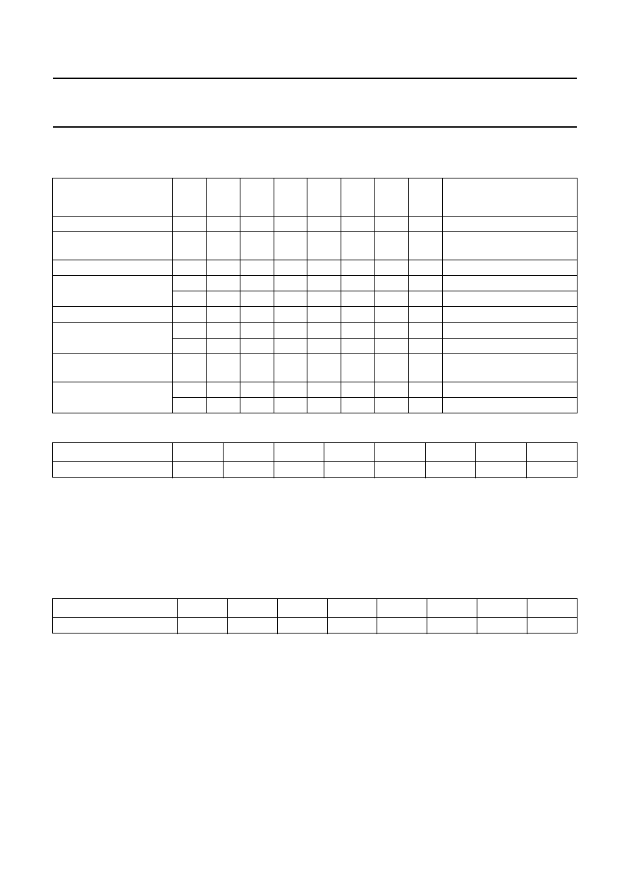
Table 1
Summary of the HTRC11001T command set
8.8.1
C
OMMAND
READ_TAG
This command is used to read the demodulated bit stream from a transponder.
After the assertion of the three command bits the HTRC11001T instantaneously switches to the READ_TAG mode and
transmits the demodulated, filtered and digitized data to the microcontroller. This data should be decoded by the
microcontroller.
The READ_TAG mode is terminated by a LOW-to-HIGH transition on pin SCLK.
8.8.2
C
OMMAND
WRITE_TAG_N
This command is used to write data to a transponder.
If bits N3 to N0 are set to 0000, the signal on pin DIN is transparently switched to the drivers. A HIGH level on pin DIN
corresponds to antenna drivers switched off and a LOW level corresponds to antenna drivers switched on.
For any binary number N between 0001 and 1111, the drivers are switched off at the next positive transition on pin DIN.
This state is held for a time interval t = N
×
T
0
(for T
0
= 8
µ
s). This method relaxes the timing resolution requirements to
the microcontroller and to the software implementation while providing an exact, selectable write pulse timing.
The WRITE_TAG mode is terminated immediately by a LOW- to-HIGH transition on pin SCLK.
COMMAND NAME
BIT 7
BIT 6
BIT5
BIT 4
BIT 3
BIT 2
BIT 1
BIT 0
REMARK
MSB
LSB
READ_TAG
1
1
1
-
-
-
-
-
READ_TAG mode
WRITE_TAG_N
0
0
0
1
N3
N2
N1
N0
WRITE_TAG mode with
pulse width programming
WRITE_TAG
1
1
0
-
-
-
-
-
WRITE_TAG mode
READ_PHASE
0
0
0
0
1
0
0
0
read command
0
0
D5
D4
D3
D2
D1
D0
response
SET_SAMPLING_TIME
1
0
D5
D4
D3
D2
D1
D0
GET_SAMPLING_TIME
0
0
0
0
0
0
1
0
read command
0
0
D5
D4
D3
D2
D1
D0
response
SET_CONFIG_PAGE
0
1
P1
P0
D3
D2
D1
D0
4
×
4 configuration bits
available
GET_CONFIG_PAGE
0
0
0
0
0
1
P1
P0
read command
X3
X2
X1
X0
D3
D2
D1
D0
response
NAME
BIT 7
BIT 6
BIT 5
BIT 4
BIT 3
BIT 2
BIT 1
BIT 0
Command bits
1
1
1
-
-
-
-
-
NAME
BIT 7
BIT 6
BIT 5
BIT 4
BIT 3
BIT 2
BIT 1
BIT 0
Command bits
0
0
0
1
N3
N2
N1
N0

2001 Nov 23
9
Philips Semiconductors
Product specification
HITAG reader chip
HTRC11001T
8.8.3
C
OMMAND
WRITE_TAG
This is the 3-bit short form of the previously described command WRITE_TAG_N. It allows to switch into the
WRITE_TAG mode with a minimum communication time.
The behaviour of the WRITE_TAG command is identical to WRITE_TAG_N with two exceptions:
·
WRITE_TAG mode is entered after assertion of the third command bit
·
No N parameter is specified with this command; instead the N value which was programmed with the most recent
WRITE_TAG_N command is used. If no WRITE_TAG_N was issued so far, a default N = 0 (transparent mode) will be
assumed.
8.8.4
C
OMMAND
READ_PHASE
This command is used to read the antenna phase, which is measured at every carrier cycle.
The response bits D5 to D0 represent the phase (coded binary).
8.8.5
C
OMMAND
SET_SAMPLING_TIME
This command specifies the demodulator sampling time t
s
. The sampling time is coded binary in bits D5 to D0.
8.8.6
C
OMMAND
GET_SAMPLING_TIME
This command is used to read back the sampling time t
s
set with SET_SAMPLING_TIME.
The response bits D5 to D0 represent the sampling time (coded binary).
NAME
BIT 7
BIT 6
BIT 5
BIT 4
BIT 3
BIT 2
BIT 1
BIT 0
Command bits
1
1
0
-
-
-
-
-
NAME
BIT 7
BIT 6
BIT 5
BIT 4
BIT 3
BIT 2
BIT 1
BIT 0
Command bits
0
0
0
0
1
0
0
0
Response bits
0
0
D5
D4
D3
D2
D1
D0
NAME
BIT 7
BIT 6
BIT 5
BIT 4
BIT 3
BIT 2
BIT 1
BIT 0
Command bits
1
0
D5
D4
D3
D2
D1
D0
NAME
BIT 7
BIT 6
BIT 5
BIT 4
BIT 3
BIT 2
BIT 1
BIT 0
Command bits
0
0
0
0
0
0
1
0
Response bits
0
0
D5
D4
D3
D2
D1
D0
2001 Nov 23
10
Philips Semiconductors
Product specification
HITAG reader chip
HTRC11001T
8.8.7
C
OMMAND
SET_CONFIG_PAGE
This command is used to set the filter and amplifier parameters (cut-off frequencies and gain factors) and to select the
operation mode. Bits P1 and P0 select one of four configuration pages.
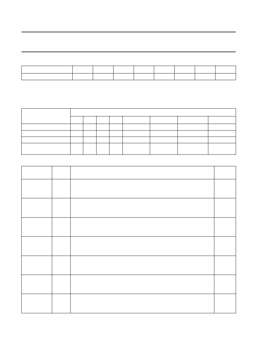
Table 2
Configuration page bit names
Table 3
Description of the configuration page bits
NAME
BIT 7
BIT 6
BIT 5
BIT 4
BIT 3
BIT 2
BIT 1
BIT 0
Command
0
1
P1
P0
D3
D2
D1
D0
COMMAND
PAGE NUMBER
BIT
7
6
P1
P0
D3
D2
D1
D0
SET_CONFIG_PAGE 0
0
1
0
0
GAIN1
GAIN0
FILTERH
FILTERL
SET_CONFIG_PAGE 1
0
1
0
1
PD_MODE
PD
HYSTERESIS
TXDIS
SET_CONFIG_PAGE 2
0
1
1
0
THRESET
ACQAMP
FREEZE1
FREEZE0
SET_CONFIG_PAGE 3
0
1
1
1
DISLP1
DISSMART-
COMP
FSEL1
FSEL0
BIT NAME
VALUE
DESCRIPTION
INITIAL
VALUE
FILTERL
main low-pass cut-off frequency
0
f
L
= 3 kHz
0
1
f
L
= 6 kHz
FILTERH
main high-pass cut-off frequency
0
f
H
= 40 kHz
0
1
f
H
= 160 kHz
GAIN0
amplifier 0 gain factor
0
gain = 16
0
1
gain = 32
GAIN1
amplifier 1 gain factor
0
gain = 6.22
1
gain = 31.5
1
TXDIS
disable coil driver
0
coil driver active
0
1
coil driver inactive
HYSTERESIS
data comparator hysteresis
0
hysteresis OFF
0
1
hysteresis ON
PD
Power-down mode enable
0
device active
0
1
device power-down

2001 Nov 23
11
Philips Semiconductors
Product specification
HITAG reader chip
HTRC11001T
PD_MODE
select Power-down mode
0
Idle mode
0
1
Power-down mode
FREEZE1,
FREEZE0
facility to achieve fast settling times (MSB and LSB)
00
normal operation
00
01
main low-pass is frozen; main high-pass is pre-charged to level on pin QGND
10
main low-pass is frozen; time constant of main high-pass is reduced by a
factor of 16 for bit FILTERH = 0 and by a factor of 8 for bit FILTERH = 1
11
main high-pass time constant is reduced by a factor of 16 for bit FILTERH = 0
and by a factor of 8 for bit FILTERH = 1; second high-pass is pre-charged
ACQAMP
store signal amplitude (see also bit AMPCOMP in Table 5)
0
set status bit AMPCOMP when the actual data signal amplitude is higher than
the stored reference
0
1
store actual amplitude of the data signal as reference for later amplitude
comparison
THRESET
reset threshold generation of digitizer
0
no reset
0
1
reset
FSEL1, FSEL0
clock frequency selection (MSB and LSB)
00
4 MHz
00
01
8 MHz
10
12 MHz
11
16 MHz
DISSMART-
COMP
disable smart comparator
0
smart comparator: on
0
1
smart comparator: off
DISLP1
disable low-pass 1
0
low-pass: on
0
1
low-pass: off
BIT NAME
VALUE
DESCRIPTION
INITIAL
VALUE
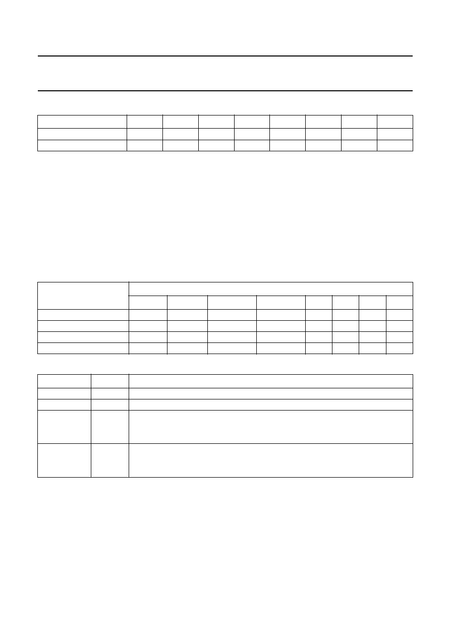
2001 Nov 23
12
Philips Semiconductors
Product specification
HITAG reader chip
HTRC11001T
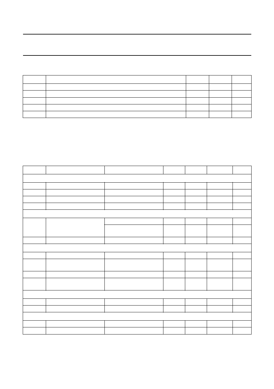
8.8.8
C
OMMAND
GET_CONFIG_PAGE
?
This command has three functions:
1. Reading back the configuration parameters set by command SET_CONFIG_PAGE
2. Reading back the transmit pulse width programmed with command WRITE_TAG_N
3. Reading the system status information.
Bits P1 and P0 select one of four configuration pages.
The response bits (X3 to X0 and D3 to D0) contains the contents of the selected configuration page in its lower nibble.
For page 0 and page 1 the higher nibble reflects the current setting of the transmit pulse width N.
For page 2 and page 3 the system status information is returned in the higher nibble.
Table 4
Configuration page bit names
Table 5
Description of the configuration page bits
NAME
BIT 7
BIT 6
BIT 5
BIT 4
BIT 3
BIT 2
BIT 1
BIT 0
Command bits
0
0
0
0
0
1
P1
P0
Response bits
X3
X2
X1
X0
D3
D2
D1
D0
COMMAND
PAGE NUMBER
BIT
X3
X2
X1
X0
3
2
1
0
GET_CONFIG_PAGE 0
N3
N2
N1
N0
D3
D2
D1
D0
GET_CONFIG_PAGE 1
N3
N2
N1
N0
D3
D2
D1
D0
GET_CONFIG_PAGE 2
0 (RFU)
0 (RFU)
AMPCOMP
ANTFAIL
D3
D2
D1
D0
GET_CONFIG_PAGE 3
0 (RFU)
0 (RFU)
AMPCOMP
ANTFAIL
D3
D2
D1
D0
BIT NAME
VALUE
DESCRIPTION
D3 to D0
XXXX
contents of the selected configuration page
N3 to N0
XXXX
current setting of the transmit pulse width
ANTFAIL
antenna failure
0
no antenna failure
1
antenna failure
AMPCOMP
amplitude comparison result (see also bit ACQAMP in Table 3)
0
actual data signal amplitude is lower than the stored reference
1
actual data signal amplitude is higher than the stored reference
2001 Nov 23
13
Philips Semiconductors
Product specification
HITAG reader chip
HTRC11001T
9
LIMITING VALUES
In accordance with the Absolute Maximum Rating System (IEC 60134); note 1.
Note
1. Stress above one or more of the limiting values may cause permanent damage to the device. These are stresses
ratings only and operation of the device at these or at any other conditions above those given in Chapter 10 not
implied. Exposure or limiting values for extended periods may affect device reliability.
10 DC CHARACTERISTICS
All voltages are measured with respect to ground (pin V
SS
); T
amb
=
-
40 to +85
°
C
Note
1. Power consumption of external quartz or any other component is not included.
SYMBOL
PARAMETER
MIN.
MAX.
UNIT
V
n
voltage at any pin (except pin RX)
-
0.3
+
6.5
V
V
n(max)
maximum voltage at any pin with respect to V
DD
(except pin RX)
-
0.3
V
DD
+ 0.3
V
V
RX
voltage at pin RX
-
10
+12
V
T
j(max)
maximum junction temperature
-
140
°
C
T
stg
storage temperature
-
65
+125
°
C
SYMBOL
PARAMETER
CONDITIONS
MIN.
TYP.
MAX.
UNIT
Supply
V
DD
supply voltage
4.5
5.0
5.5
V
I
DD
supply current
V
DD
= 5.5 V; I
TX1
= I
TX2
= 0
-
4
10
mA
I
idle
idle current
V
DD
= 5.5 V; note 1
-
0.2
0.4
mA
I
pd
power-down current
V
DD
= 5.5 V
-
7
20
µ
A
Driver outputs (pins TX1 and TX2)
I
ant(p)
antenna driver output current
(peak value)
permanent
-
-
200
mA
pulse load; t
on
< 400 ms;
ratio on : off = 1 : 4
-
-
400
mA
R
o
output resistance
both drivers together
-
2.5
7
Demodulator input (pin RX)
V
I
input voltage
with respect to pin QGND
-
8
-
+8
V
V
diag
diagnosis level voltage
with respect to pin QGND;
V
DD
= 5 V
-
1.5
-
1.15
-
0.8
V
V
QGND
potential on pin QGND
0.35V
DD
0.42V
DD
0.50V
DD
V
R
i
internal demodulator
impedance
17
25
33
k
Digital inputs
V
IH
HIGH-level input voltage
0.7V
DD
-
V
DD
+ 0.3 V V
V
IL
LOW-level input voltage
-
0.3
-
0.3V
DD
V
Digital outputs
V
OL
LOW-level output voltage
I
OL(max)
= 1 mA
-
-
0.4
V
I
OL
LOW-level output current
V
OL
0.4 V
1
-
-
mA

2001 Nov 23
14
Philips Semiconductors
Product specification
HITAG reader chip
HTRC11001T
11 AC CHARACTERISTICS
T
amb
=
-
40 to +85
°
C.
Note
1. These short times require special command sequences. Please refer to the application note
"AN 98080 Read/Write
devices based on the HITAG Read/Write IC HTRC110".
SYMBOL
PARAMETER
CONDITIONS
MIN.
TYP.
MAX.
UNIT
Oscillator inputs (pins XTAL1 and XTAL2)
f
osc
oscillator frequency
depending on bits FSEL1
and FSEL0
4
-
16
MHz
t
st
start-up time
-
4
10
ms
C
i
input capacitance on pin XTAL1
-
5
-
pF
R
i
input resistance
between pins XTAL1
and XTAL2
0.9
1.3
3.0
M
External clock input (pin XTAL1)
f
ext
external clock frequency
depending on bits FSEL1
and FSEL0
4
-
16
MHz
duty cycle
40
-
60
%
Serial interface
t
su
set-up time
pin MODE at V
SS
50
-
-
ns
t
h
hold time
pin MODE at V
SS
50
-
-
ns
Receiver (pin RX)
V
RX(p-p)
sensitivity (peak-to-peak value)
receiver input
2
1
-
mV
t
d
receiver delay
bit FILTERL = 0
290
310
340
µ
s
bit FILTERL = 1
160
175
190
µ
s
Demodulator valid time
t
rec
demodulator recovery time
after clock stable; note 1
-
-
5
ms
after WRITE-pulse; note 1
-
-
500
µ
s
after AST-step
-
0.7
1.5
ms
phase measurement error
-
-
±
5.7
deg
2001 Nov 23
15
Philips Semiconductors
Product specification
HITAG reader chip
HTRC11001T
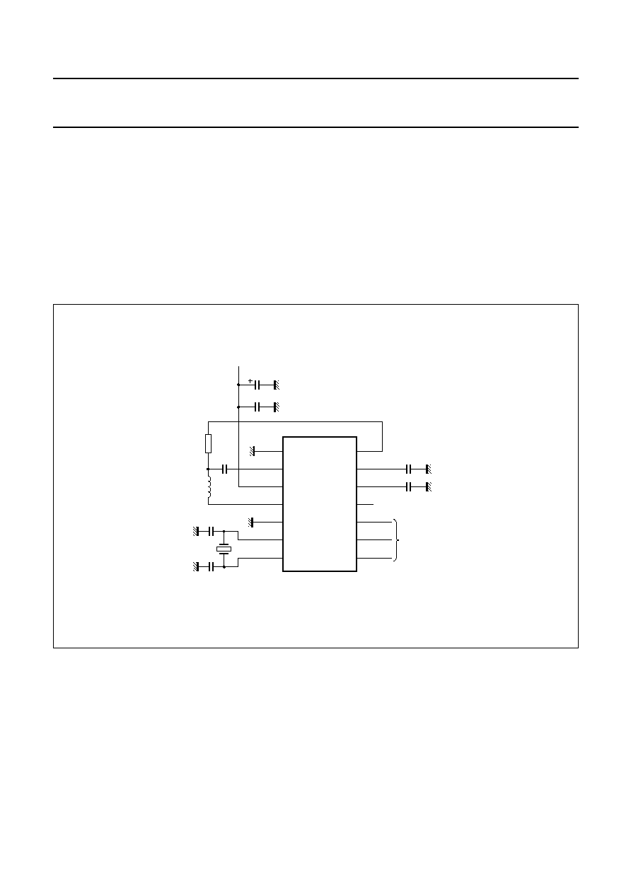
12 APPLICATION INFORMATION
Figure 4 shows a minimal application circuitry for the
HTRC11001T.
The reader coil L
a
together with the capacitor C
a
forms a
series resonant LC circuit (f
0
= 125 kHz). The high
voltages in the LC circuit are divided to safe operating
levels by R
v
and the internal resistor R
i
behind pin RX.
The two capacitors connected to pin XTAL1 and
pin XTAL2 shall be the recommended values and types
from the data sheet of the crystal.
Alternatively to a crystal, a ceramic resonator can be used
or an external clock source can be connected to
pin XTAL1.
handbook, full pagewidth
MGW267
100 nF
100 nF
10
µ
F
100 nF
HTRC11001T
1
2
3
4
5
6
7
8
14
13
12
11
10
9
VSS
TX2
VDD
VDD
TX1
MODE
XTAL1
XTAL2
SCLK
DIN
DOUT
to microcontroller
n.c.
CEXT
QGND
RX
Rv
Ca
La
Fig.4 Minimum application circuitry.
2001 Nov 23
16
Philips Semiconductors
Product specification
HITAG reader chip
HTRC11001T
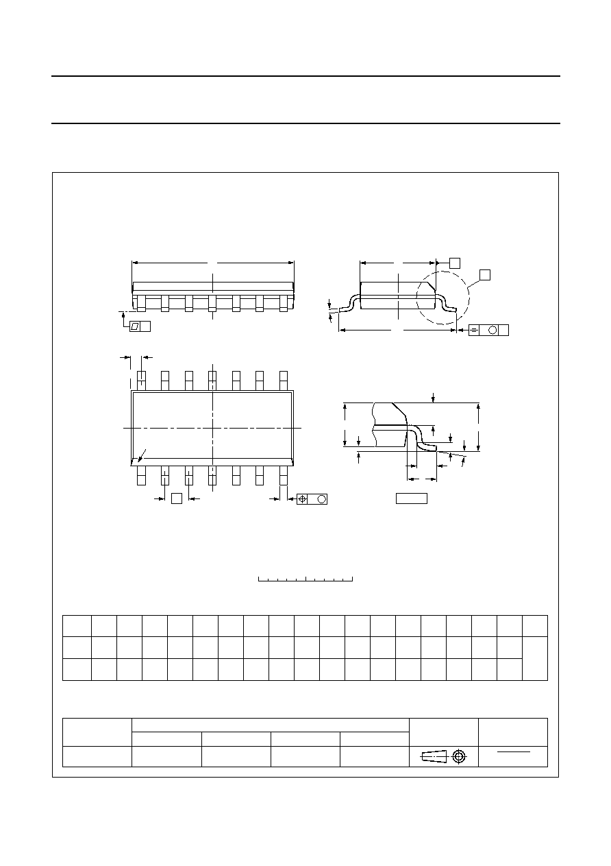
13 PACKAGE OUTLINE
UNIT
A
max.
A
1
A
2
A
3
b
p
c
D
(1)
E
(1)
(1)
e
H
E
L
L
p
Q
Z
y
w
v
REFERENCES
OUTLINE
VERSION
EUROPEAN
PROJECTION
ISSUE DATE
IEC
JEDEC
EIAJ
mm
inches
1.75
0.25
0.10
1.45
1.25
0.25
0.49
0.36
0.25
0.19
8.75
8.55
4.0
3.8
1.27
6.2
5.8
0.7
0.6
0.7
0.3
8
0
o
o
0.25
0.1
DIMENSIONS (inch dimensions are derived from the original mm dimensions)
Note
1. Plastic or metal protrusions of 0.15 mm maximum per side are not included.
1.0
0.4
SOT108-1
X
w
M
A
A
1
A
2
b
p
D
H
E
L
p
Q
detail X
E
Z
e
c
L
v
M
A
(A )
3
A
7
8
1
14
y
076E06
MS-012
pin 1 index
0.069
0.010
0.004
0.057
0.049
0.01
0.019
0.014
0.0100
0.0075
0.35
0.34
0.16
0.15
0.050
1.05
0.041
0.244
0.228
0.028
0.024
0.028
0.012
0.01
0.25
0.01
0.004
0.039
0.016
97-05-22
99-12-27
0
2.5
5 mm
scale
SO14: plastic small outline package; 14 leads; body width 3.9 mm
SOT108-1

2001 Nov 23
17
Philips Semiconductors
Product specification
HITAG reader chip
HTRC11001T
14 SOLDERING
14.1
Introduction to soldering surface mount
packages
This text gives a very brief insight to a complex technology.
A more in-depth account of soldering ICs can be found in
our
"Data Handbook IC26; Integrated Circuit Packages"
(document order number 9398 652 90011).
There is no soldering method that is ideal for all surface
mount IC packages. Wave soldering can still be used for
certain surface mount ICs, but it is not suitable for fine pitch
SMDs. In these situations reflow soldering is
recommended.
14.2
Reflow soldering
Reflow soldering requires solder paste (a suspension of
fine solder particles, flux and binding agent) to be applied
to the printed-circuit board by screen printing, stencilling or
pressure-syringe dispensing before package placement.
Several methods exist for reflowing; for example,
convection or convection/infrared heating in a conveyor
type oven. Throughput times (preheating, soldering and
cooling) vary between 100 and 200 seconds depending
on heating method.
Typical reflow peak temperatures range from
215 to 250
°
C. The top-surface temperature of the
packages should preferable be kept below 220
°
C for
thick/large packages, and below 235
°
C for small/thin
packages.
14.3
Wave soldering
Conventional single wave soldering is not recommended
for surface mount devices (SMDs) or printed-circuit boards
with a high component density, as solder bridging and
non-wetting can present major problems.
To overcome these problems the double-wave soldering
method was specifically developed.
If wave soldering is used the following conditions must be
observed for optimal results:
·
Use a double-wave soldering method comprising a
turbulent wave with high upward pressure followed by a
smooth laminar wave.
·
For packages with leads on two sides and a pitch (e):
larger than or equal to 1.27 mm, the footprint
longitudinal axis is preferred to be parallel to the
transport direction of the printed-circuit board;
smaller than 1.27 mm, the footprint longitudinal axis
must be parallel to the transport direction of the
printed-circuit board.
The footprint must incorporate solder thieves at the
downstream end.
·
For packages with leads on four sides, the footprint must
be placed at a 45
°
angle to the transport direction of the
printed-circuit board. The footprint must incorporate
solder thieves downstream and at the side corners.
During placement and before soldering, the package must
be fixed with a droplet of adhesive. The adhesive can be
applied by screen printing, pin transfer or syringe
dispensing. The package can be soldered after the
adhesive is cured.
Typical dwell time is 4 seconds at 250
°
C.
A mildly-activated flux will eliminate the need for removal
of corrosive residues in most applications.
14.4
Manual soldering
Fix the component by first soldering two
diagonally-opposite end leads. Use a low voltage (24 V or
less) soldering iron applied to the flat part of the lead.
Contact time must be limited to 10 seconds at up to
300
°
C.
When using a dedicated tool, all other leads can be
soldered in one operation within 2 to 5 seconds between
270 and 320
°
C.

2001 Nov 23
18
Philips Semiconductors
Product specification
HITAG reader chip
HTRC11001T
14.5
Suitability of surface mount IC packages for wave and reflow soldering methods
Notes
1. All surface mount (SMD) packages are moisture sensitive. Depending upon the moisture content, the maximum
temperature (with respect to time) and body size of the package, there is a risk that internal or external package
cracks may occur due to vaporization of the moisture in them (the so called popcorn effect). For details, refer to the
Drypack information in the
"Data Handbook IC26; Integrated Circuit Packages; Section: Packing Methods".
2. These packages are not suitable for wave soldering as a solder joint between the printed-circuit board and heatsink
(at bottom version) can not be achieved, and as solder may stick to the heatsink (on top version).
3. If wave soldering is considered, then the package must be placed at a 45
°
angle to the solder wave direction.
The package footprint must incorporate solder thieves downstream and at the side corners.
4. Wave soldering is only suitable for LQFP, TQFP and QFP packages with a pitch (e) equal to or larger than 0.8 mm;
it is definitely not suitable for packages with a pitch (e) equal to or smaller than 0.65 mm.
5. Wave soldering is only suitable for SSOP and TSSOP packages with a pitch (e) equal to or larger than 0.65 mm; it is
definitely not suitable for packages with a pitch (e) equal to or smaller than 0.5 mm.
PACKAGE
SOLDERING METHOD
WAVE
REFLOW
(1)
BGA, HBGA, LFBGA, SQFP, TFBGA
not suitable
suitable
HBCC, HLQFP, HSQFP, HSOP, HTQFP, HTSSOP, HVQFN, SMS
not suitable
(2)
suitable
PLCC
(3)
, SO, SOJ
suitable
suitable
LQFP, QFP, TQFP
not recommended
(3)(4)
suitable
SSOP, TSSOP, VSO
not recommended
(5)
suitable

2001 Nov 23
19
Philips Semiconductors
Product specification
HITAG reader chip
HTRC11001T
15 DATA SHEET STATUS
Notes
1. Please consult the most recently issued data sheet before initiating or completing a design.
2. The product status of the device(s) described in this data sheet may have changed since this data sheet was
published. The latest information is available on the Internet at URL http://www.semiconductors.philips.com.
DATA SHEET STATUS
(1)
PRODUCT
STATUS
(2)
DEFINITIONS
Objective data
Development
This data sheet contains data from the objective specification for product
development. Philips Semiconductors reserves the right to change the
specification in any manner without notice.
Preliminary data
Qualification
This data sheet contains data from the preliminary specification.
Supplementary data will be published at a later date. Philips
Semiconductors reserves the right to change the specification without
notice, in order to improve the design and supply the best possible
product.
Product data
Production
This data sheet contains data from the product specification. Philips
Semiconductors reserves the right to make changes at any time in order
to improve the design, manufacturing and supply. Changes will be
communicated according to the Customer Product/Process Change
Notification (CPCN) procedure SNW-SQ-650A.
16 DEFINITIONS
Short-form specification
The data in a short-form
specification is extracted from a full data sheet with the
same type number and title. For detailed information see
the relevant data sheet or data handbook.
Limiting values definition
Limiting values given are in
accordance with the Absolute Maximum Rating System
(IEC 60134). Stress above one or more of the limiting
values may cause permanent damage to the device.
These are stress ratings only and operation of the device
at these or at any other conditions above those given in the
Characteristics sections of the specification is not implied.
Exposure to limiting values for extended periods may
affect device reliability.
Application information
Applications that are
described herein for any of these products are for
illustrative purposes only. Philips Semiconductors make
no representation or warranty that such applications will be
suitable for the specified use without further testing or
modification.
17 DISCLAIMERS
Life support applications
These products are not
designed for use in life support appliances, devices, or
systems where malfunction of these products can
reasonably be expected to result in personal injury. Philips
Semiconductors customers using or selling these products
for use in such applications do so at their own risk and
agree to fully indemnify Philips Semiconductors for any
damages resulting from such application.
Right to make changes
Philips Semiconductors
reserves the right to make changes, without notice, in the
products, including circuits, standard cells, and/or
software, described or contained herein in order to
improve design and/or performance. Philips
Semiconductors assumes no responsibility or liability for
the use of any of these products, conveys no licence or title
under any patent, copyright, or mask work right to these
products, and makes no representations or warranties that
these products are free from patent, copyright, or mask
work right infringement, unless otherwise specified.

© Koninklijke Philips Electronics N.V. 2001
SCA73
All rights are reserved. Reproduction in whole or in part is prohibited without the prior written consent of the copyright owner.
The information presented in this document does not form part of any quotation or contract, is believed to be accurate and reliable and may be changed
without notice. No liability will be accepted by the publisher for any consequence of its use. Publication thereof does not convey nor imply any license
under patent- or other industrial or intellectual property rights.
Philips Semiconductors a worldwide company
Contact information
For additional information please visit http://www.semiconductors.philips.com.
Fax: +31 40 27 24825
For sales offices addresses send e-mail to: sales.addresses@www.semiconductors.philips.com.
Printed in The Netherlands
613502/02/pp
20
Date of release:
2001 Nov 23
Document order number:
9397 750 08329
Document Outline
- 1 FEATURES
- 2 APPLICATIONS
- 3 GENERAL DESCRIPTION
- 4 QUICK REFERENCE DATA
- 5 ORDERING INFORMATION
- 6 BLOCK DIAGRAM
- 7 PINNING
- 8 FUNCTIONAL DESCRIPTION
- 8.1 Power supply
- 8.2 Antenna drivers
- 8.3 Diagnosis
- 8.4 Oscillator with programmable divider
- 8.5 Adaptive sampling time demodulator
- 8.6 Idle and Power-down mode
- 8.7 Serial interface
- 8.8 Commands
- 9 LIMITING VALUES
- 10 DC CHARACTERISTICS
- 11 AC CHARACTERISTICS
- 12 APPLICATION INFORMATION
- 13 PACKAGE OUTLINE
- 14 SOLDERING
- 15 DATA SHEET STATUS
- 16 DEFINITIONS
- 17 DISCLAIMERS