 | –≠–ª–µ–∫—Ç—Ä–æ–Ω–Ω—ã–π –∫–æ–º–ø–æ–Ω–µ–Ω—Ç: OQ2536HP | –°–∫–∞—á–∞—Ç—å:  PDF PDF  ZIP ZIP |

DATA SHEET
Product specification
File under Integrated Circuits, IC19
1998 Mar 10
INTEGRATED CIRCUITS
OQ2536HP
SDH/SONET STM16/OC48
demultiplexer
1998 Mar 10
2
Philips Semiconductors
Product specification
SDH/SONET STM16/OC48 demultiplexer
OQ2536HP
FEATURES
∑
Normal and loop (test) modes
∑
1.2 V GTL (Gunning Transceiver Logic) level compatible
data and clock outputs (low speed interface)
∑
Differential CML (Current-Mode Logic) data and clock
inputs
∑
High input sensitivity (100 mV for the high speed inputs)
∑
Boundary Scan Test (BST) at low speed interface, in
accordance with
"IEEE Std 1149.1-1990"
∑
Low power dissipation (typically 1.45 W).
DESCRIPTION
The OQ2536HP is a 32-channel demultiplexer intended
for use in STM16/OC48 applications. It demultiplexes a
single 2.5 Gbits/s input channel to 32
◊
78 Mbits/s output
channels. The data and clock outputs on the low speed
interface are GTL compatible, while the high speed data
and clock inputs are CML compatible.
ORDERING INFORMATION
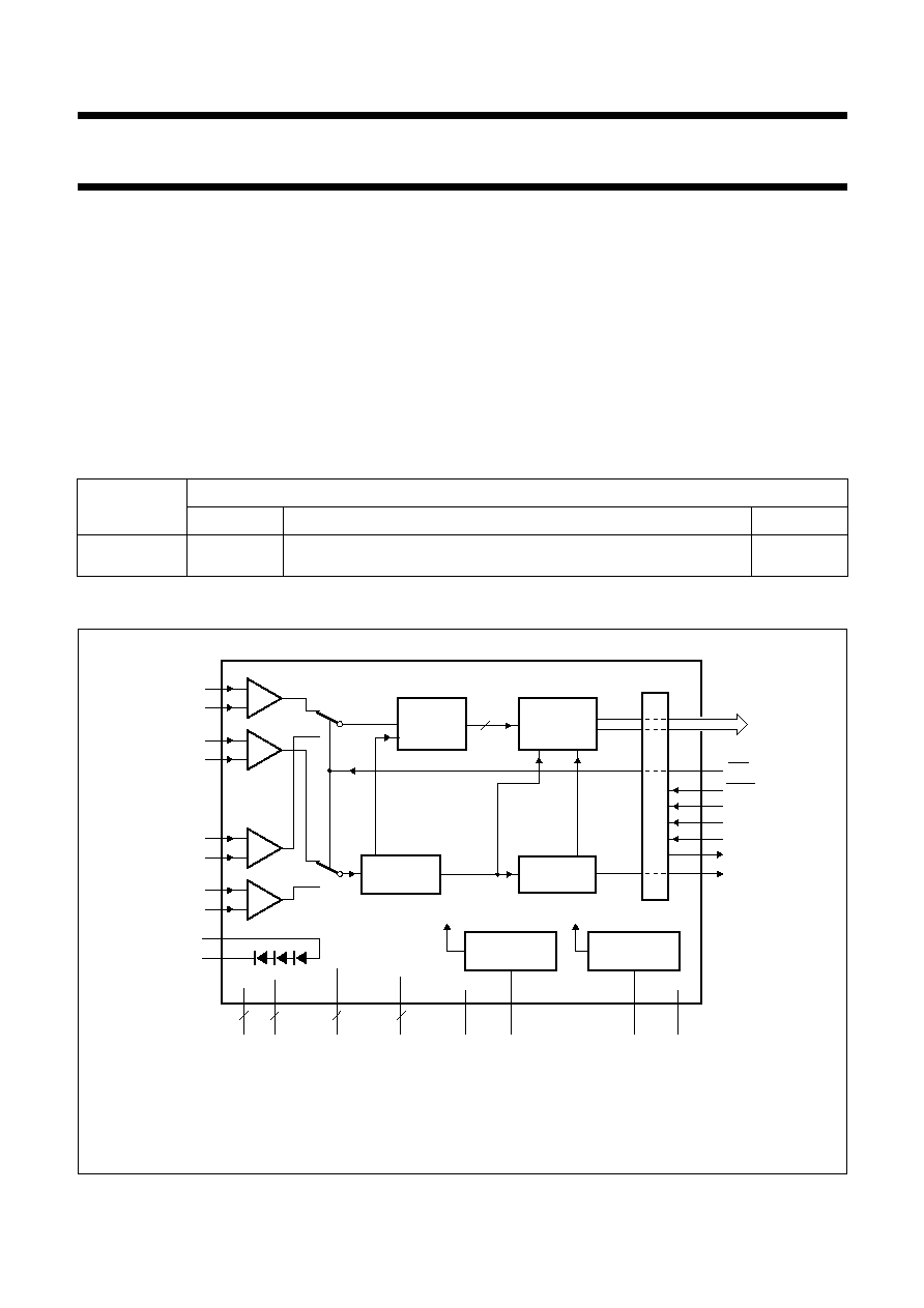
BLOCK DIAGRAM
TYPE
NUMBER
PACKAGE
NAME
DESCRIPTION
VERSION
OQ2536HP
HLQFP100
plastic heat-dissipating low profile quad flat package; 100 leads; body
14
◊
14
◊
1.4 mm
SOT470-1
Fig.1 Block diagram.
(1) See Chapter "Pinning" for D0 to D31 pin numbers.
(2) Pins 1, 8, 17, 22, 25, 29, 33, 35, 40 to 50, 52, 55, 58, 61, 64, 67, 78, 82, 91 and 96.
handbook, full pagewidth
4
ENL
TRST
TMS
TCK
TDI
TDO
CDIV
DIN
DINQ
CIN
CINQ
DLOOP
DLOOPQ
CLOOP
CLOOPQ
DIOA
DIOC
1 : 4 DMUX
DIVIDE BY 4
622 MHz
OQ2536HP
78 MHz
2.5 GHz
BAND GAP
REFERENCE 1
DIVIDE BY 8
BST LOGIC
4
◊
1 : 8 DMUX
622
Mbits/s
2.5 Gbits/s
78
Mbits/s
75
70
72
69
68
71
12
26, 27, 28,
76, 77
13, 14, 36,
37, 63, 85,
86
11, 38, 39,
62, 88
VDD
VCC1
VEE
VCC2
BGCAP1
29
5
7
5
(2)
(1)
GND
74
51
BAND GAP
REFERENCE 2
BGCAP2
34
73
REFC
54
53
56
57
65
66
60
59
32
31
D0
to
D31
MGK346

1998 Mar 10
3
Philips Semiconductors
Product specification
SDH/SONET STM16/OC48 demultiplexer
OQ2536HP
PINNING
SYMBOL
PIN
TYPE
(1)
DESCRIPTION
GND
1
S
ground
D29
2
O
78 Mbits/s data output channel for D29
D25
3
O
78 Mbits/s data output channel for D25
D21
4
O
78 Mbits/s data output channel for D21
D17
5
O
78 Mbits/s data output channel for D17
D13
6
O
78 Mbits/s data output channel for D13
D9
7
O
78 Mbits/s data output channel for D9
GND
8
S
ground
D5
9
O
78 Mbits/s data output channel for D5
D1
10
O
78 Mbits/s data output channel for D1
V
EE
11
S
supply voltage (
-
4.5 V)
CDIV
12
O
78 MHz clock output
V
CC2
13
S
supply voltage (+1.5 V)
V
CC2
14
S
supply voltage (+1.5 V)
D28
15
O
78 Mbits/s data output channel for D28
D24
16
O
78 Mbits/s data output channel for D24
GND
17
S
ground
D20
18
O
78 Mbits/s data output channel for D20
D16
19
O
78 Mbits/s data output channel for D16
D12
20
O
78 Mbits/s data output channel for D12
D8
21
O
78 Mbits/s data output channel for D8
GND
22
S
ground
D4
23
O
78 Mbits/s data output channel for D4
D0
24
O
78 Mbits/s data output channel for D0
GND
25
S
ground
V
DD
26
I
supply voltage (+3.3 V)
V
DD
27
I
supply voltage (+3.3 V)
V
DD
28
I
supply voltage (+3.3 V)
GND
29
S
ground
i.c.
30
-
internally connected, to be left open-circuit
DIOC
31
A
cathode of temperature diode array
DIOA
32
A
anode of temperature diode array
GND
33
S
ground
BGCAP2
34
A
pin for connecting external band gap decoupling capacitor (4
◊
1 : 8 DMUX)
GND
35
S
ground
V
CC2
36
S
supply voltage (+1.5 V)
V
CC2
37
S
supply voltage (+1.5 V)
V
EE
38
S
supply voltage (
-
4.5 V)
V
EE
39
S
supply voltage (
-
4.5 V)
GND
40
S
ground

1998 Mar 10
4
Philips Semiconductors
Product specification
SDH/SONET STM16/OC48 demultiplexer
OQ2536HP
GND
41
S
ground
GND
42
S
ground
GND
43
S
ground
GND
44
S
ground
GND
45
S
ground
GND
46
S
ground
GND
47
S
ground
GND
48
S
ground
GND
49
S
ground
GND
50
S
ground
BGCAP1
51
A
pin for connecting external band gap decoupling capacitor (1 : 4 DMUX)
GND
52
S
ground
DINQ
53
I
inverted data input in normal mode
DIN
54
I
data input in normal mode
GND
55
S
ground
CIN
56
I
clock input in normal mode
CINQ
57
I
inverted clock input in normal mode
GND
58
S
ground
CLOOPQ
59
I
inverted clock input from multiplexer IC OQ2535 (loop mode)
CLOOP
60
I
clock input from multiplexer IC OQ2535 (loop mode)
GND
61
S
ground
V
EE
62
S
supply voltage (
-
4.5 V)
V
CC2
63
S
supply voltage (+1.5 V)
GND
64
S
ground
DLOOP
65
I
data input from multiplexer IC OQ2535 (loop mode)
DLOOPQ
66
I
inverted data input from multiplexer IC OQ2535 (loop mode)
GND
67
S
ground
TRST
68
I
test RESET input for BST mode (active LOW)
TMS
69
I
test mode select input for BST
TCK
70
I
test clock input for BST mode
TDO
71
O
serial test data output for BST mode
TDI
72
I
serial test data input for BST mode
REFC
73
A
pin for connecting external reference decoupling capacitor (for standard TTL
reference)
V
CC1
74
S
supply voltage (+5.0 V)
ENL
75
I
loop mode enable input (active LOW)
V
DD
76
I
supply voltage (+3.3 V)
V
DD
77
I
supply voltage (+3.3 V)
GND
78
S
ground
D31
79
O
78 Mbits/s data output channel for D31
D27
80
O
78 Mbits/s data output channel for D27
SYMBOL
PIN
TYPE
(1)
DESCRIPTION

1998 Mar 10
5
Philips Semiconductors
Product specification
SDH/SONET STM16/OC48 demultiplexer
OQ2536HP
Note
1. Pin type abbreviations: O = Output, I = Input, S = power Supply, A = Analog function.
D23
81
O
78 Mbits/s data output channel for D23
GND
82
S
ground
D19
83
O
78 Mbits/s data output channel for D19
D15
84
O
78 Mbits/s data output channel for D15
V
CC2
85
S
supply voltage (+1.5 V)
V
CC2
86
S
supply voltage (+1.5 V)
D11
87
O
78 Mbits/s data output channel for D11
V
EE
88
S
supply voltage (
-
4.5 V)
D7
89
O
78 Mbits/s data output channel for D7
D3
90
O
78 Mbits/s data output channel for D3
GND
91
S
ground
D30
92
O
78 Mbits/s data output channel for D30
D26
93
O
78 Mbits/s data output channel for D26
D22
94
O
78 Mbits/s data output channel for D22
D18
95
O
78 Mbits/s data output channel for D18
GND
96
S
ground
D14
97
O
78 Mbits/s data output channel for D14
D10
98
O
78 Mbits/s data output channel for D10
D6
99
O
78 Mbits/s data output channel for D6
D2
100
O
78 Mbits/s data output channel for D2
SYMBOL
PIN
TYPE
(1)
DESCRIPTION
1998 Mar 10
6
Philips Semiconductors
Product specification
SDH/SONET STM16/OC48 demultiplexer
OQ2536HP
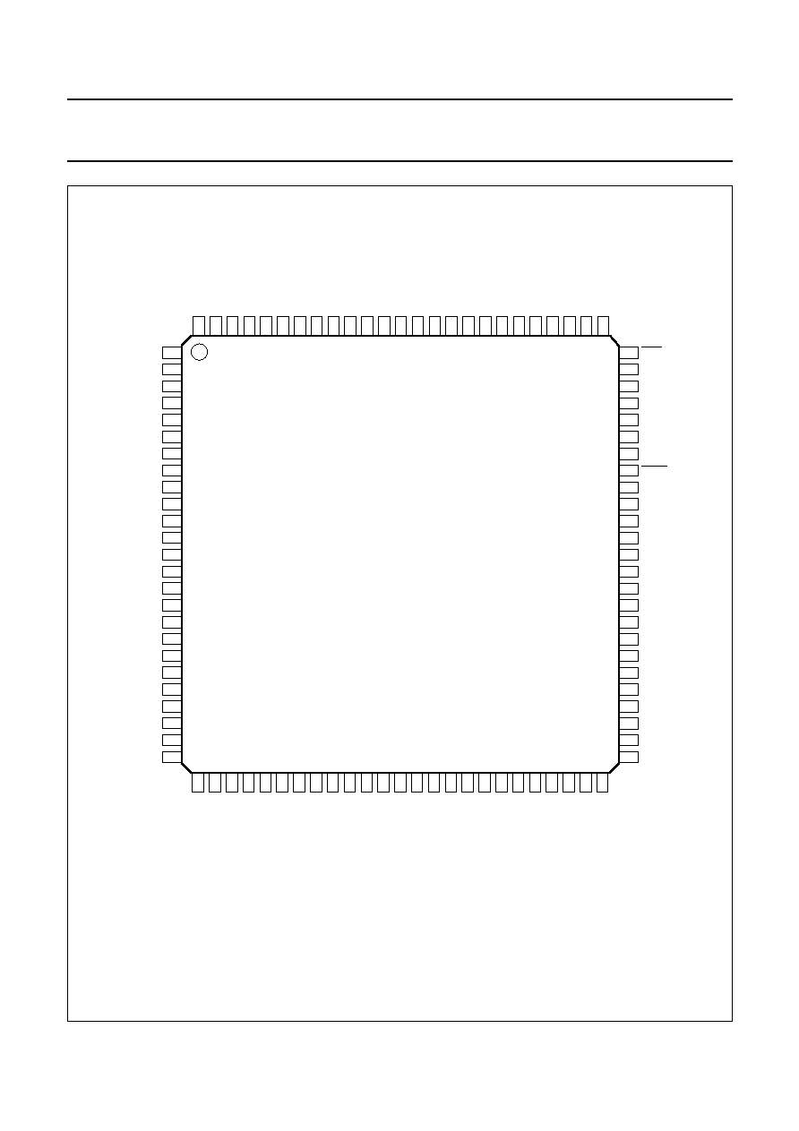
Fig.2 Pin configuration.
handbook, full pagewidth
75
74
73
72
71
70
69
68
67
66
65
64
63
62
61
60
59
58
57
56
55
54
53
52
51
80
79
78
77
76
ENL
VCC1
REFC
TDI
TDO
TCK
TMS
TRST
GND
DLOOPQ
DLOOP
GND
VCC2
VEE
GND
CLOOP
CLOOPQ
GND
CINQ
CIN
GND
DIN
DINQ
GND
BGCAP1
MGK345
GND
D29
D25
D21
D17
D13
D9
GND
D5
D1
VEE
CDIV
VCC2
VCC2
D28
D24
GND
D20
D16
D12
D8
GND
D4
D0
GND
D27
D31
GND
V
DD
V
DD
D2
D6
D10
D14
GND
D18
D22
D26
D30
GND
D3
D7
V
EE
D11
V
CC2
V
CC2
D15
D19
GND
D23
DIOC
DIOA
GND
BGCAP2
GND
V
CC2
V
CC2
V
EE
V
EE
GND
GND
GND
GND
GND
GND
GND
GND
GND
GND
GND
V
DD
V
DD
V
DD
GND
i.c.
30
29
28
27
26
25
24
23
22
21
20
19
18
17
16
15
14
13
12
11
10
9
8
7
6
5
4
3
2
1
100
99
98
97
96
95
94
93
92
91
90
89
88
87
86
85
84
83
82
81
31
32
33
34
35
36
37
38
39
40
41
42
43
44
45
46
47
48
49
50
OQ2536HP

1998 Mar 10
7
Philips Semiconductors
Product specification
SDH/SONET STM16/OC48 demultiplexer
OQ2536HP
FUNCTIONAL DESCRIPTION
The OQ2536HP is a 32-channel demultiplexer, intended
for use in STM16/OC48 applications. It demultiplexes a
single 2.5 Gbits/s input channel to 32
◊
78 Mbits/s output
channels.
The demultiplexing is performed in two stages.
The 2.5 Gbits/s data channel is first demultiplexed to four
622 Mbits/s data channels. Each of these channels is then
fed to a 1 : 8 demultiplexer to generate 32
◊
78 Mbits/s
output channels.
The ENL control input is used for switching between
normal and loop modes. When loop mode is enabled
(ENL = LOW), inputs DLOOP, DLOOPQ, CLOOP and
CLOOPQ are selected. In normal mode (ENL = HIGH),
inputs DIN, DINQ, CIN and CINQ are selected.
The signal applied to CIN and CINQ is a 2.5 GHz
recovered clock signal, e.g. coming from the OQ2541 data
and clock recovery IC. The clock is divided down to
78 MHz, which is used for receive logic timing and is
available as a GTL compatible output at pin CDIV.
High bit rate stage: 1 : 4 DMUX
The 2.5 Gbits/s data stream is fed into a 1 : 4
demultiplexer to generate four 622 Mbits/s channels.
The input pins DIN, DINQ, DLOOP, DLOOPQ, CIN, CINQ,
CLOOP and CLOOPQ are terminated internally with 50
resistors to GND.
Low bit rate part: 4
◊
1 : 8 DMUX
The four 622 Mbits/s output channels coming from the
high bit rate stage are loaded into four 8-bit shift registers.
The 622 MHz clock for these shift registers comes from the
preceding stage.
The 32 bits contained in the shift registers are loaded into
latches and made available on outputs D0 to D31. These
outputs are 1.2 V GTL compatible and have internal 100
pull up resistors. The 78 MHz clock output, CDIV, has an
internal 50
pull up resistor.
The first serial data bit coming in at DIN or DLOOP is given
out at pin D31 (MSB) and so on.
The data outputs may not always represent four STM
bytes. This is because the internal load pulse for the output
latches is not synchronized to the STM16 frame.
Power supply connections
The power supply pins need to be individually decoupled
using chip capacitors mounted as close as possible to the
IC. If multiple decoupling capacitors are used for a single
supply node, large distance between the capacitances
should be avoided in order to avoid resonance.
To minimize low frequency switching noise in the vicinity of
the OQ2536HP, all power supply lines should be filtered
once by an LC-circuit with a low cutoff frequency
(as shown in the application diagram, Fig.7).
Ground connection
The ground connection on the PCB needs to be a large
copper area fill connected to a common ground plane with
low inductance.
RF connections
A coupled stripline or microstrip with an odd mode
characteristic impedance of 50
(nominal value) should
be used for the RF connections on the PCB.
The connections should be kept as short as possible. This
applies to the CML differential line pairs CIN and CINQ,
DIN and DINQ, CLOOP and CLOOPQ, and DLOOP and
DLOOPQ. In addition, the following lines should not vary in
length by more than 5 mm:
∑
CIN, CINQ, DIN and DINQ
∑
DLOOP, DLOOPQ, CLOOP and CLOOPQ.
Interface to receive logic
The 78 Mbits/s interface lines, CDIV and D0 to D31,
should not exceed 50 mm in length. The parasitic
capacitance of these lines should be as small as possible
(less than 3 pF is desirable).
ESD protection
All pads are protected by ESD protection diodes, with the
exception of the high frequency inputs DIN, DINQ,
DLOOP, DLOOPQ, CIN, CINQ, CLOOP and CLOOPQ.
Cooling
In many cases it is necessary to mount a special cooling
device on the package. The thermal resistance from
junction to case, R
th j-c
and from junction to ambient, R
th j-a
,
are given in Chapter "Thermal characteristics". Since the
heat-slug in the package is connected to the die, the
cooling device should be electrically isolated.
To calculate if a heatsink is necessary, the maximum
allowed total thermal resistance R is calculated as:
(1)
R
th
T
j
T
amb
≠
P
tot
------------------------
=

1998 Mar 10
8
Philips Semiconductors
Product specification
SDH/SONET STM16/OC48 demultiplexer
OQ2536HP
where:
R
th
= total thermal resistance from junction to ambient
in the application
T
j
= junction temperature
T
amb
= ambient temperature.
As long as R
th
is greater than R
th j-a
of the OQ2536HP
including environmental conditions like air flow and board
layout, no heatsink is necessary. For example if
T
j
= 120
∞
C, T
amb
= 70
∞
C and P
tot
= 1.45 W, then:
(2)
which is more than the worst case R
th j-a
= 33 K/W, so no
heatsink is necessary.
Another example; if for safety reasons T
j
should stay as
low as 110
∞
C, while T
amb
= 85
∞
C and P
tot
= 2 W, then:
(3)
In this case extra cooling is needed. The thermal
resistance of the heatsink is calculated as follows:
(4)
where:
R
th h-a
= thermal resistance from heatsink to ambient
R
th c-h
= thermal resistance from case to heatsink
R
th j-c
= thermal resistance from junction to case,
see Chapter "Thermal characteristics".
R
th
120
70
≠
(
)
1.45
-----------------------------
34.4
=
=
K W
/
[
]
R
th
110
85
≠
(
)
2.0
-----------------------------
12.5
=
=
K W
/
[
]
R
thh
a
≠
1
R
th
--------
1
R
thj
a
≠
-----------------
≠
1
≠
R
thj
c
≠
≠
R
thc
h
≠
≠
If for instance R
th c-h
= 0.5 K/W and R
th j -a
= 33 K/W then:
(5)
Built in temperature sensor
Three series-connected diodes have been integrated for
measuring junction temperature. The diode array,
accessed by means of the DIOA (anode) and DIOC
(cathode) pins, has a temperature dependency of
approximately
-
6 mV/
∞
C. With a diode current of 1 mA,
the voltage will be somewhere in the range 1.7 to 2.5 V,
depending on temperature.
Boundary Scan Test (BST) interface
Boundary scan test logic has been implemented for all
digital inputs and outputs on the low frequency interface, in
accordance with
"IEEE Std 1149.1-1990". All scan tests
other than SAMPLE mode are available. The boundary
scan test logic consists of a TAP controller, a BYPASS
register, a 2-bit instruction register, a 32-bit identification
register and a 36-bit boundary scan register (the last two
are combined). The architecture of the TAP controller and
the BYPASS register is in accordance with IEEE
recommendations.
The four command modes, selected be means of the
instruction register, are: EXTEST (00), PRELOAD (01),
IDCODE (10) and BYPASS (11).
All boundary scan test inputs, TDI, TMS, TCK and TRST,
have internal pull up resistors. The maximum test clock
frequency at TCK is 12 MHz.
R
thh
a
≠
1
12.5
-----------
1
33
------
≠
1
≠
3.1
≠
17.0
K W
/
[
]
Table 1
BST identifier code
Notes
1. LSB is shifted out first on the TDO pin.
2. The manufacturer's code was implemented incorrectly. It should have been 0000 0010 101.
VERSION
OQ
2536 (BINARY)
PHILIPS SEMICONDUCTORS
LSB
(1)
0001
01
00 1001 1110 1000
0000 0011 101
(2)
1

1998 Mar 10
9
Philips Semiconductors
Product specification
SDH/SONET STM16/OC48 demultiplexer
OQ2536HP
Table 2
BST bit order
Note
1. LSB is shifted out first on the TDO pin.
BIT NUMBER
SYMBOL
PIN
33 (MSB)
D31
79
32
D27
80
31
D23
81
30
D19
83
29
D15
84
28
D11
87
27
D7
89
26
D3
90
25
D30
92
24
D26
93
23
D22
94
22
D18
95
21
D14
97
20
D10
98
19
D6
99
18
D2
100
17
D29
2
16
D25
3
15
D21
4
14
D17
5
13
D13
6
12
D9
7
11
D5
9
10
D1
10
9
CDIV
12
8
D28
15
7
D24
16
6
D20
18
5
D16
19
4
D12
20
3
D8
21
2
D4
23
1
D0
24
0 (LSB)
(1)
ENL
75
1998 Mar 10
10
Philips Semiconductors
Product specification
SDH/SONET STM16/OC48 demultiplexer
OQ2536HP
LIMITING VALUES
In accordance with the Absolute Maximum Rating System (IEC 134).
THERMAL CHARACTERISTICS
Note
1. The thermal resistance from junction to ambient is strongly depending on the board design and airflow. The values
given in the table are typical values and are measured on a single sided test board with dimensions of
76
◊
114
◊
1.6 mm. Better values can be obtained when mounted on multilayer boards with large ground planes.
SYMBOL
PARAMETER
MIN.
MAX.
UNIT
V
CC1
supply voltage
-
0.5
+6.0
V
V
EE
supply voltage
-
6.0
+0.5
V
V
DD
supply voltage
-
0.5
+5.0
V
V
CC2
supply voltage
-
0.5
+2.0
V
V
n
DC voltage
pins 2 to 7, 9, 10, 15, 16, 18 to 21, 23, 24, 79, 80, 81, 83, 84, 87, 89,
90, 92 to 95 and 97 to 100
0.0
2.0
V
pins 53, 54, 56, 57, 59, 60, 65 and 66
-
1.0
+0.5
V
pins 68, 69, 70, 72, 73 and 75
-
0.5
V
CC1
+ 0.5
V
pins 30, 34 and 51
V
EE
-
0.5
0.5
V
pins 31and 32
V
EE
-
0.5
V
CC1
+ 0.5
V
I
n
DC current
pins 2 to 7, 9, 10, 15, 16, 18 to 21, 23, 24, 79, 80, 81, 83, 84, 87, 89,
90, 92 to 95, and 97 to 100
-
15
mA
pin 12
-
30
mA
pins 31 and 32
-
10
mA
pin 71
-
50
mA
P
tot
total power dissipation
-
2.6
W
T
j
junction temperature
-
120
∞
C
T
stg
storage temperature
-
65
+150
∞
C
SYMBOL
PARAMETER
CONDITIONS
VALUE
UNIT
R
th j-c
thermal resistance from junction to case
2.6
K/W
R
th j-a
thermal resistance from junction to
ambient
see note 1
airflow = 0 ft/min
33
K/W
airflow = 100 ft/min
28
K/W
airflow = 200 ft/min
25
K/W
airflow = 400 ft/min
22
K/W
airflow = 600 ft/min
20
K/W
1998 Mar 10
11
Philips Semiconductors
Product specification
SDH/SONET STM16/OC48 demultiplexer
OQ2536HP
DC CHARACTERISTICS
Typical values at T
amb
= 25
∞
C and at typical supply voltages; minimum and maximum values are valid over the entire
ambient temperature range and supply voltage range.
SYMBOL
PARAMETER
CONDITIONS
MIN.
TYP.
MAX.
UNIT
General
V
CC1
supply voltage
4.75
5.0
5.25
V
V
EE
supply voltage
-
4.75
-
4.5
-
4.25
V
V
DD
supply voltage
3.14
3.3
3.47
V
V
CC2
supply voltage
1.1
1.5
1.6
V
I
CC1
supply current
-
14
22
mA
I
EE
supply current
-
170
215
mA
I
DD
supply current
-
100
185
mA
I
CC2
supply current
note 1
-
190
525
mA
P
tot
total power dissipation
note 1
-
1.45
2.6
W
T
j
junction temperature
-
-
+120
∞
C
T
amb
ambient temperature
-
40
-
+85
∞
C
TTL input: ENL
V
IL
LOW-level input voltage
-
-
0.8
V
V
IH
HIGH-level input voltage
2.0
-
-
V
I
IL
LOW-level input current
-
90
-
-
µ
A
I
IH
HIGH-level input current
-
-
210
µ
A
TTL inputs: TDI, TCK, TMS and TRST; note 2
V
IL
LOW-level input voltage
-
-
0.4
V
V
IH
HIGH-level input voltage
2.0
-
-
V
CML inputs: CIN, CINQ, DIN, DINQ, CLOOP, CLOOPQ, DLOOP and DLOOPQ; note 3
V
i(p-p)
input voltage (peak-to-peak value)
50
measurement
system
100
250
500
mV
V
IO
permitted input offset voltage
-
25
-
+25
mV
V
I,IQ
input voltages
-
600
-
+250
mV
Z
i
single ended input impedance
for DC signal
-
50
-
TTL output: TDO; note 4
V
OL
LOW-level output voltage
I
OL
= 4 mA
-
0.3
0.5
V
1998 Mar 10
12
Philips Semiconductors
Product specification
SDH/SONET STM16/OC48 demultiplexer
OQ2536HP
Notes
1. Maximum current I
CC2
and maximum power dissipation P
tot
are worst case figures i.e. data outputs D0 to D31 remain
in LOW state.
2. TDI, TCK, TMS and TRST are connected via 90 k
to V
DD
.
3. See Fig.3 for symbol definitions.
4. TDO is switched to high impedance state if BST is inactive.
5. Output CDIV has an internal pull-up resistor of 50
to V
CC2
. Outputs D0 to D31 have internal pull-up resistors of
100
to V
CC2
.
6. The first serial data bit coming in at DIN or DLOOP is given out at D31 (MSB) and so on.
7. The HIGH-level output voltage depends on the supply voltage V
CC2
.
8. The temperature diode array can be used to measure the temperature of the die. The temperature dependency of
this voltage is approximately
-
6 mV/K.
V
OH
HIGH-level output voltage
I
OH
=
-
400
µ
A
2.4
4.0
-
V
I
OZ
output current in high impedance state
-
-
1
µ
A
Outputs: CDIV and D0 to D31; notes 5 and 6
V
OL
LOW-level output voltage
Open outputs
-
0.3
0.4
V
V
OH
HIGH-level output voltage; note 7
1.1
1.5
1.6
V
Temperature diode array
V
DIOA-DIOC
diode voltage range
(8)
I
I(d)
= 1 mA
-
2.1
-
V
SYMBOL
PARAMETER
CONDITIONS
MIN.
TYP.
MAX.
UNIT
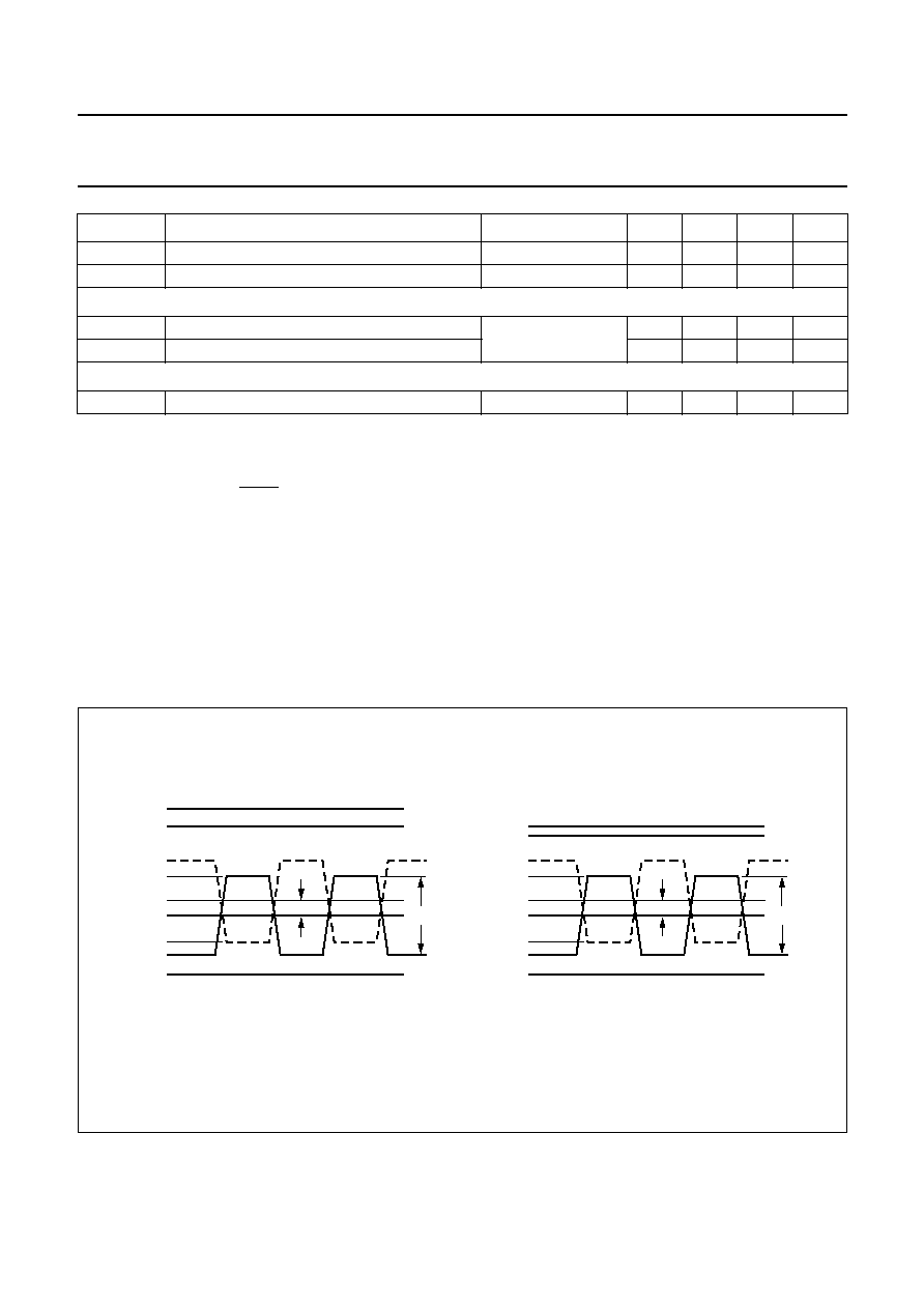
Fig.3 Logic level symbol definitions for CML.
handbook, full pagewidth
MGK144
VIO
VI(max)
VIQH
VIH
VIQL
VIL
VI(min)
Vi (p-p)
GND
CML INPUT
VOO
VO(max)
VOQH
VOH
VOQL
VOL
VO(min)
Vo (p-p)
GND
CML OUTPUT
1998 Mar 10
13
Philips Semiconductors
Product specification
SDH/SONET STM16/OC48 demultiplexer
OQ2536HP
TIMING
Typical values at T
amb
= 25
∞
C and at typical supply voltages; minimum and maximum values are valid over the entire
ambient temperature range and supply voltage range.
Notes
1. The specified timing characteristics are applicable in both normal and loop modes.
2. A capacitive load of 15 pF was connected at all outputs. An input reference level of 1 V was used.
SYMBOL
PARAMETER
CONDITIONS
MIN.
TYP.
MAX.
UNIT
CML input timing; note 1; Fig.5
f
clk(CIN)
input clock frequency
2.488
-
-
GHz
t
su
input data set-up time
140
-
-
ps
t
h
input data hold time
80
-
-
ps
SR
CIN
clock slew rate
1
-
-
V/ns
TTL output timing; note 2; Fig.6
f
clk(CDIV)
output clock frequency
f
clk(CDIV)
= 2.488 GHz
-
77.76
-
MHz
CDIV
output clock duty factor
-
50
-
%
t
r(CDIV)
output clock rise time
Measured between
10% and 90% levels
of full output swing
-
-
2700
ps
t
f(CDIV)
output clock fall time
-
-
1000
ps
t
r(D0 to D31)
data out rise time
-
-
5100
ps
t
f(D0 to D31)
data out fall time
-
-
1000
ps
t
CDV
clock edge to data valid time
-
-
2700
ps
t
DI
data invalid time
-
-
2850
ps
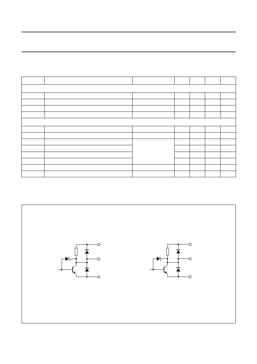
Fig.4 GTL output circuits.
handbook, halfpage
MBK756
VCC2
D0 to D31
GND
100
handbook, halfpage
MBK757
VCC2
CDIV
GND
50
1998 Mar 10
14
Philips Semiconductors
Product specification
SDH/SONET STM16/OC48 demultiplexer
OQ2536HP
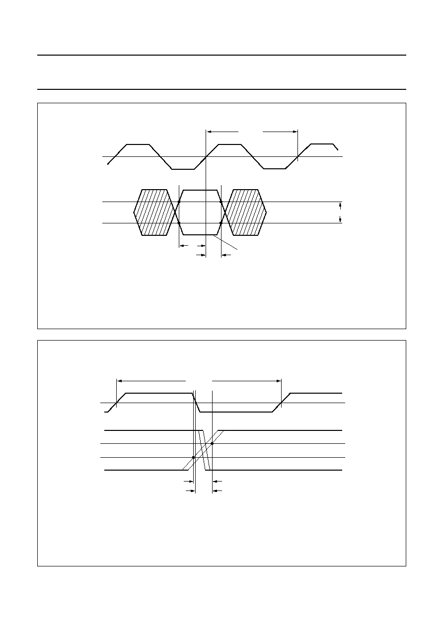
Fig.5 CML input timing.
handbook, full pagewidth
th
tsu
100 mV
valid data
50%
DIN
CIN
Tcy(CIN)
MGK347
Fig.6 Output timing.
handbook, full pagewidth
MGK348
tCDV
tDI
Tcy(CDIV)
1.0 V
CDIV
D0 to D31
1.1 V
0.9 V
1998 Mar 10
15
Philips Semiconductors
Product specification
SDH/SONET STM16/OC48 demultiplexer
OQ2536HP
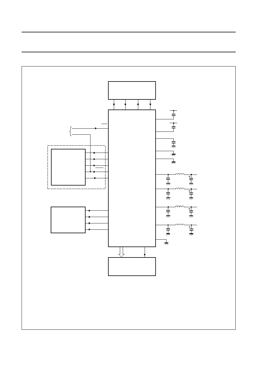
APPLICATION INFORMATION
Fig.7 Application diagram.
(1) V
CC2
pins 13, 14, 36, 37, 63, 85 and 86 should be connected together, and to the filter network.
(2) V
DD
pins 26, 27, 28, 76 and 77 should be connected together, and to the filter network.
(3) V
EE
pins 11, 38, 39, 62 and 8 should be connected together, and to the filter network.
(4) All GND pins (pins 1, 4, 8, 9, 11, 15, 17, 21, 25, 36, 40, 56, 64, 67, 70, 73, 76, 77, 79, 80, 81, 84, 89, 92 to 98 and 100) must be connected directly
to the PCB ground plane.
handbook, full pagewidth
MGK349
ferrite
bead
ferrite
bead
ferrite
bead
ferrite
bead
1
µ
F
100
nF
TMS
TCK
TDO
TDI
DIN
DINQ
CIN
CINQ
DIOA
DLOOP
DLOOPQ
CLOOP
VCC2
CLOOPQ
DLOOP
DLOOPQ
CLOOP
CLOOPQ
RECEIVE LOGIC
BOUNDARY SCAN
TEST EQUIPMENT
micro-
controller
OQ2535
MUX
OQ2541
OQ2536
68
75
69
70
72
71
VEE
GND
54
53
56
DATA AND CLOCK RECOVERY
57
D
DQ
CL
CLQ
65
66
60
59
ENL
TRST
(3)
1
µ
F
100
nF
VDD
(2)
74
(1)
32
73
34
51
12
1
µ
F
100
nF
1
µ
F
100
nF
DIOC
31
REFC
BGCAP2
33 nF
10 nF
VCC1
VEE
BGCAP1
CDIV
10 nF
D0 to D31
C78
D0 to D31
VEE
(4)
1998 Mar 10
16
Philips Semiconductors
Product specification
SDH/SONET STM16/OC48 demultiplexer
OQ2536HP
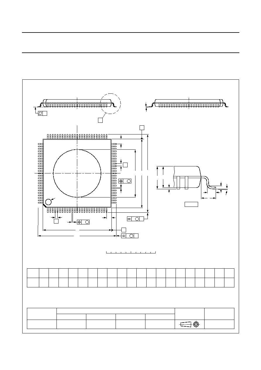
PACKAGE OUTLINE
UNIT
A
max.
A
1
A
2
A
3
b
p
c
E
(1)
e
H
E
L
L
p
Z
y
w
v
REFERENCES
OUTLINE
VERSION
EUROPEAN
PROJECTION
ISSUE DATE
IEC
JEDEC
EIAJ
mm
1.6
0.20
0.05
1.5
1.3
0.25
0.28
0.16
0.18
0.12
14.1
13.9
0.5
16.25
15.75
1.15
0.85
7
0
o
o
0.12
0.1
0.2
1.0
J
(2)
DIMENSIONS (mm are the original dimensions)
Notes
1. Plastic or metal protrusions of 0.25 mm maximum per side are not included.
2. Heatsink intrusion 0.0127 maximum.
0.75
0.45
10.15
9.15
SOT470-1
97-01-13
D
(1)
(1)
(1)
14.1
13.9
H
D
16.25
15.75
E
Z
1.15
0.85
D
b
p
e
E
detail X
J
B
25
c
D
H
b
p
E
H
A
1
A
A
2
v
M
B
D
ZD
A
Z E
e
v
M
A
X
1
100
76
75
51
50
26
L
p
L
(A )
3
y
w
M
w
M
0
5
10 mm
scale
HLQFP100: plastic heat-dissipating low profile quad flat package;
100 leads; body 14 x 14 x 1.4 mm
SOT470-1
pin 1 index

1998 Mar 10
17
Philips Semiconductors
Product specification
SDH/SONET STM16/OC48 demultiplexer
OQ2536HP
SOLDERING
Introduction
There is no soldering method that is ideal for all IC
packages. Wave soldering is often preferred when
through-hole and surface mounted components are mixed
on one printed-circuit board. However, wave soldering is
not always suitable for surface mounted ICs, or for
printed-circuits with high population densities. In these
situations reflow soldering is often used.
This text gives a very brief insight to a complex technology.
A more in-depth account of soldering ICs can be found in
our
"IC Package Databook" (order code 9398 652 90011).
Reflow soldering
Reflow soldering techniques are suitable for all LQFP
packages.
Reflow soldering requires solder paste (a suspension of
fine solder particles, flux and binding agent) to be applied
to the printed-circuit board by screen printing, stencilling or
pressure-syringe dispensing before package placement.
Several techniques exist for reflowing; for example,
thermal conduction by heated belt. Dwell times vary
between 50 and 300 seconds depending on heating
method. Typical reflow temperatures range from
215 to 250
∞
C.
Preheating is necessary to dry the paste and evaporate
the binding agent. Preheating duration: 45 minutes at
45
∞
C.
Wave soldering
Wave soldering is not recommended for LQFP packages.
This is because of the likelihood of solder bridging due to
closely-spaced leads and the possibility of incomplete
solder penetration in multi-lead devices.
If wave soldering cannot be avoided, the following
conditions must be observed:
∑
A double-wave (a turbulent wave with high upward
pressure followed by a smooth laminar wave)
soldering technique should be used.
∑
The footprint must be at an angle of 45
∞
to the board
direction and must incorporate solder thieves
downstream and at the side corners.
Even with these conditions, do not consider wave
soldering LQFP packages LQFP48 (SOT313-2),
LQFP64 (SOT314-2) or LQFP80 (SOT315-1).
During placement and before soldering, the package must
be fixed with a droplet of adhesive. The adhesive can be
applied by screen printing, pin transfer or syringe
dispensing. The package can be soldered after the
adhesive is cured.
Maximum permissible solder temperature is 260
∞
C, and
maximum duration of package immersion in solder is
10 seconds, if cooled to less than 150
∞
C within
6 seconds. Typical dwell time is 4 seconds at 250
∞
C.
A mildly-activated flux will eliminate the need for removal
of corrosive residues in most applications.
Repairing soldered joints
Fix the component by first soldering two diagonally-
opposite end leads. Use only a low voltage soldering iron
(less than 24 V) applied to the flat part of the lead. Contact
time must be limited to 10 seconds at up to 300
∞
C. When
using a dedicated tool, all other leads can be soldered in
one operation within 2 to 5 seconds between
270 and 320
∞
C.

1998 Mar 10
18
Philips Semiconductors
Product specification
SDH/SONET STM16/OC48 demultiplexer
OQ2536HP
DEFINITIONS
LIFE SUPPORT APPLICATIONS
These products are not designed for use in life support appliances, devices, or systems where malfunction of these
products can reasonably be expected to result in personal injury. Philips customers using or selling these products for
use in such applications do so at their own risk and agree to fully indemnify Philips for any damages resulting from such
improper use or sale.
Data sheet status
Objective specification
This data sheet contains target or goal specifications for product development.
Preliminary specification
This data sheet contains preliminary data; supplementary data may be published later.
Product specification
This data sheet contains final product specifications.
Limiting values
Limiting values given are in accordance with the Absolute Maximum Rating System (IEC 134). Stress above one or
more of the limiting values may cause permanent damage to the device. These are stress ratings only and operation
of the device at these or at any other conditions above those given in the Characteristics sections of the specification
is not implied. Exposure to limiting values for extended periods may affect device reliability.
Application information
Where application information is given, it is advisory and does not form part of the specification.

1998 Mar 10
19
Philips Semiconductors
Product specification
SDH/SONET STM16/OC48 demultiplexer
OQ2536HP
NOTES

Internet: http://www.semiconductors.philips.com
Philips Semiconductors ≠ a worldwide company
© Philips Electronics N.V. 1998
SCA57
All rights are reserved. Reproduction in whole or in part is prohibited without the prior written consent of the copyright owner.
The information presented in this document does not form part of any quotation or contract, is believed to be accurate and reliable and may be changed
without notice. No liability will be accepted by the publisher for any consequence of its use. Publication thereof does not convey nor imply any license
under patent- or other industrial or intellectual property rights.
Netherlands: Postbus 90050, 5600 PB EINDHOVEN, Bldg. VB,
Tel. +31 40 27 82785, Fax. +31 40 27 88399
New Zealand: 2 Wagener Place, C.P.O. Box 1041, AUCKLAND,
Tel. +64 9 849 4160, Fax. +64 9 849 7811
Norway: Box 1, Manglerud 0612, OSLO,
Tel. +47 22 74 8000, Fax. +47 22 74 8341
Philippines: Philips Semiconductors Philippines Inc.,
106 Valero St. Salcedo Village, P.O. Box 2108 MCC, MAKATI,
Metro MANILA, Tel. +63 2 816 6380, Fax. +63 2 817 3474
Poland: Ul. Lukiska 10, PL 04-123 WARSZAWA,
Tel. +48 22 612 2831, Fax. +48 22 612 2327
Portugal: see Spain
Romania: see Italy
Russia: Philips Russia, Ul. Usatcheva 35A, 119048 MOSCOW,
Tel. +7 095 755 6918, Fax. +7 095 755 6919
Singapore: Lorong 1, Toa Payoh, SINGAPORE 1231,
Tel. +65 350 2538, Fax. +65 251 6500
Slovakia: see Austria
Slovenia: see Italy
South Africa: S.A. PHILIPS Pty Ltd., 195-215 Main Road Martindale,
2092 JOHANNESBURG, P.O. Box 7430 Johannesburg 2000,
Tel. +27 11 470 5911, Fax. +27 11 470 5494
South America: Al. Vicente Pinzon, 173, 6th floor,
04547-130 S√O PAULO, SP, Brazil,
Tel. +55 11 821 2333, Fax. +55 11 821 2382
Spain: Balmes 22, 08007 BARCELONA,
Tel. +34 3 301 6312, Fax. +34 3 301 4107
Sweden: Kottbygatan 7, Akalla, S-16485 STOCKHOLM,
Tel. +46 8 632 2000, Fax. +46 8 632 2745
Switzerland: Allmendstrasse 140, CH-8027 ZÐRICH,
Tel. +41 1 488 2686, Fax. +41 1 488 3263
Taiwan: Philips Semiconductors, 6F, No. 96, Chien Kuo N. Rd., Sec. 1,
TAIPEI, Taiwan Tel. +886 2 2134 2865, Fax. +886 2 2134 2874
Thailand: PHILIPS ELECTRONICS (THAILAND) Ltd.,
209/2 Sanpavuth-Bangna Road Prakanong, BANGKOK 10260,
Tel. +66 2 745 4090, Fax. +66 2 398 0793
Turkey: Talatpasa Cad. No. 5, 80640 GÐLTEPE/ISTANBUL,
Tel. +90 212 279 2770, Fax. +90 212 282 6707
Ukraine: PHILIPS UKRAINE, 4 Patrice Lumumba str., Building B, Floor 7,
252042 KIEV, Tel. +380 44 264 2776, Fax. +380 44 268 0461
United Kingdom: Philips Semiconductors Ltd., 276 Bath Road, Hayes,
MIDDLESEX UB3 5BX, Tel. +44 181 730 5000, Fax. +44 181 754 8421
United States: 811 East Arques Avenue, SUNNYVALE, CA 94088-3409,
Tel. +1 800 234 7381
Uruguay: see South America
Vietnam: see Singapore
Yugoslavia: PHILIPS, Trg N. Pasica 5/v, 11000 BEOGRAD,
Tel. +381 11 625 344, Fax.+381 11 635 777
For all other countries apply to: Philips Semiconductors,
International Marketing & Sales Communications, Building BE-p, P.O. Box 218,
5600 MD EINDHOVEN, The Netherlands, Fax. +31 40 27 24825
Argentina: see South America
Australia: 34 Waterloo Road, NORTH RYDE, NSW 2113,
Tel. +61 2 9805 4455, Fax. +61 2 9805 4466
Austria: Computerstr. 6, A-1101 WIEN, P.O. Box 213, Tel. +43 160 1010,
Fax. +43 160 101 1210
Belarus: Hotel Minsk Business Center, Bld. 3, r. 1211, Volodarski Str. 6,
220050 MINSK, Tel. +375 172 200 733, Fax. +375 172 200 773
Belgium: see The Netherlands
Brazil: see South America
Bulgaria: Philips Bulgaria Ltd., Energoproject, 15th floor,
51 James Bourchier Blvd., 1407 SOFIA,
Tel. +359 2 689 211, Fax. +359 2 689 102
Canada: PHILIPS SEMICONDUCTORS/COMPONENTS,
Tel. +1 800 234 7381
China/Hong Kong: 501 Hong Kong Industrial Technology Centre,
72 Tat Chee Avenue, Kowloon Tong, HONG KONG,
Tel. +852 2319 7888, Fax. +852 2319 7700
Colombia: see South America
Czech Republic: see Austria
Denmark: Prags Boulevard 80, PB 1919, DK-2300 COPENHAGEN S,
Tel. +45 32 88 2636, Fax. +45 31 57 0044
Finland: Sinikalliontie 3, FIN-02630 ESPOO,
Tel. +358 9 615800, Fax. +358 9 61580920
France: 51 Rue Carnot, BP317, 92156 SURESNES Cedex,
Tel. +33 1 40 99 6161, Fax. +33 1 40 99 6427
Germany: Hammerbrookstraþe 69, D-20097 HAMBURG,
Tel. +49 40 23 53 60, Fax. +49 40 23 536 300
Greece: No. 15, 25th March Street, GR 17778 TAVROS/ATHENS,
Tel. +30 1 4894 339/239, Fax. +30 1 4814 240
Hungary: see Austria
India: Philips INDIA Ltd, Band Box Building, 2nd floor,
254-D, Dr. Annie Besant Road, Worli, MUMBAI 400 025,
Tel. +91 22 493 8541, Fax. +91 22 493 0966
Indonesia: see Singapore
Ireland: Newstead, Clonskeagh, DUBLIN 14,
Tel. +353 1 7640 000, Fax. +353 1 7640 200
Israel: RAPAC Electronics, 7 Kehilat Saloniki St, PO Box 18053,
TEL AVIV 61180, Tel. +972 3 645 0444, Fax. +972 3 649 1007
Italy: PHILIPS SEMICONDUCTORS, Piazza IV Novembre 3,
20124 MILANO, Tel. +39 2 6752 2531, Fax. +39 2 6752 2557
Japan: Philips Bldg 13-37, Kohnan 2-chome, Minato-ku, TOKYO 108,
Tel. +81 3 3740 5130, Fax. +81 3 3740 5077
Korea: Philips House, 260-199 Itaewon-dong, Yongsan-ku, SEOUL,
Tel. +82 2 709 1412, Fax. +82 2 709 1415
Malaysia: No. 76 Jalan Universiti, 46200 PETALING JAYA, SELANGOR,
Tel. +60 3 750 5214, Fax. +60 3 757 4880
Mexico: 5900 Gateway East, Suite 200, EL PASO, TEXAS 79905,
Tel. +9-5 800 234 7381
Middle East: see Italy
Printed in The Netherlands
425102/200/01/pp20
Date of release: 1998 Mar 10
Document order number:
9397 750 01623