 | –≠–ª–µ–∫—Ç—Ä–æ–Ω–Ω—ã–π –∫–æ–º–ø–æ–Ω–µ–Ω—Ç: P32P4910 | –°–∫–∞—á–∞—Ç—å:  PDF PDF  ZIP ZIP |

HC05H12GRS/D
Rev. 1.0
NON-DISCLOSURE AGREEMENT REQUIRED
68HC(7)05H12
General Release Specification
Rev. 1.0
November, 1998

NON-DISCLOSURE AGREEMENT REQUIRED
General Release Specification
General Release Specification
MC68HC(7)05H12
--
Rev. 1.0
2
MOTOROLA
Motorola reserves the right to make changes without further notice to
any products herein to improve reliability, function or design. Motorola
does not assume any liability arising out of the application or use of any
product or circuit described herein; neither does it convey any license
under its patent rights nor the rights of others. Motorola products are not
designed, intended, or authorized for use as components in systems
intended for surgical implant into the body, or other applications intended
to support or sustain life, or for any other application in which the failure
of the Motorola product could create a situation where personal injury or
death may occur. Should Buyer purchase or use Motorola products for
any such unintended or unauthorized application, Buyer shall indemnify
and hold Motorola and its officers, employees, subsidiaries, affiliates,
and distributors harmless against all claims, costs, damages, and
expenses, and reasonable attorney fees arising out of, directly or
indirectly, any claim of personal injury or death associated with such
unintended or unauthorized use, even if such claim alleges that Motorola
was negligent regarding the design or manufacture of the part.
© Motorola, Inc., 1997

MC68HC(7)05H12
--
Rev. 1.0
General Release Specification
MOTOROLA
List of Sections
1
NON-DISCLOSURE AGREEMENT REQUIRED
General Release Specification -- MC68HC(7)05H12
List of Sections
List of Sections . . . . . . . . . . . . . . . . . . . . . . . . . . . . . . . . . . 1
Table of Contents. . . . . . . . . . . . . . . . . . . . . . . . . . . . . . . . 3
List of Figures . . . . . . . . . . . . . . . . . . . . . . . . . . . . . . . . . . 11
List of Tables . . . . . . . . . . . . . . . . . . . . . . . . . . . . . . . . . . . 15
General Description . . . . . . . . . . . . . . . . . . . . . . . . . . . . 17
Memory . . . . . . . . . . . . . . . . . . . . . . . . . . . . . . . . . . . . . . 25
CPU and Instruction Set. . . . . . . . . . . . . . . . . . . . . . . . . . 37
Interrupts. . . . . . . . . . . . . . . . . . . . . . . . . . . . . . . . . . . . . . 59
Resets . . . . . . . . . . . . . . . . . . . . . . . . . . . . . . . . . . . . . . . . 67
Operating Modes . . . . . . . . . . . . . . . . . . . . . . . . . . . . . . 75
Input/Output Ports . . . . . . . . . . . . . . . . . . . . . . . . . . . . . . 79
Core Timer . . . . . . . . . . . . . . . . . . . . . . . . . . . . . . . . . . . . 97
16-Bit Timers . . . . . . . . . . . . . . . . . . . . . . . . . . . . . . . . . . 103
Serial Peripheral Interface (SPI) . . . . . . . . . . . . . . . . . . 115
Serial Communications Interface (SCI). . . . . . . . . . . . 125
Analog to Digital Converter . . . . . . . . . . . . . . . . . . . . . 143
EEPROM. . . . . . . . . . . . . . . . . . . . . . . . . . . . . . . . . . . . . . 153

NON-DISCLOSURE AGREEMENT REQUIRED
List of Sections
General Release Specification
MC68HC(7)05H12
--
Rev. 1.0
2
List of Sections
MOTOROLA
Pulse Width Modulator (PWM) . . . . . . . . . . . . . . . . . . . 159
EPROM . . . . . . . . . . . . . . . . . . . . . . . . . . . . . . . . . . . . . . 167
Electrical Characteristics . . . . . . . . . . . . . . . . . . . . . . . 173
Mechanical Specifications. . . . . . . . . . . . . . . . . . . . . . 183
Index. . . . . . . . . . . . . . . . . . . . . . . . . . . . . . . . . . . . . . . . 185

MC68HC(7)05H12
--
Rev. 1.0
General Release Specification
MOTOROLA
Table of Contents
3
NON-DISCLOSURE AGREEMENT REQUIRED
General Release Specification -- MC68HC(7)05H12
Table of Contents
Section 1. General Description
1.1
Contents . . . . . . . . . . . . . . . . . . . . . . . . . . . . . . . . . . . . . . . . . . 17
1.2
Introduction . . . . . . . . . . . . . . . . . . . . . . . . . . . . . . . . . . . . . . . . 17
1.3
Features . . . . . . . . . . . . . . . . . . . . . . . . . . . . . . . . . . . . . . . . . . 18
1.4
Mask Options . . . . . . . . . . . . . . . . . . . . . . . . . . . . . . . . . . . . . . 20
1.5
Pin Assignments . . . . . . . . . . . . . . . . . . . . . . . . . . . . . . . . . . . . 20
1.6
Functional Pin Description . . . . . . . . . . . . . . . . . . . . . . . . . . . . 21
1.6.1
VDD and VSS . . . . . . . . . . . . . . . . . . . . . . . . . . . . . . . . . . . 21
1.6.2
AVDD . . . . . . . . . . . . . . . . . . . . . . . . . . . . . . . . . . . . . . . . . 21
1.6.3
OSC1, OSC2. . . . . . . . . . . . . . . . . . . . . . . . . . . . . . . . . . . . 21
1.6.4
RESET . . . . . . . . . . . . . . . . . . . . . . . . . . . . . . . . . . . . . . . . 21
1.6.5
IRQ/VPP . . . . . . . . . . . . . . . . . . . . . . . . . . . . . . . . . . . . . . . 21
1.6.6
PA0≠PA7/Keyboard Interrupt . . . . . . . . . . . . . . . . . . . . . . . 22
1.6.7
PB0≠PB7/ECLK, MISO, MOSI, SCK. . . . . . . . . . . . . . . . . . 22
1.6.8
PC0≠PC7/TCAP0≠3, TCMP0≠1, RDI, TDO . . . . . . . . . . . . 22
1.6.9
PD0≠PD3/AN0≠AN3 . . . . . . . . . . . . . . . . . . . . . . . . . . . . . . 23
1.6.10
VREFH . . . . . . . . . . . . . . . . . . . . . . . . . . . . . . . . . . . . . . . . 23
1.6.11
PE0≠PE7. . . . . . . . . . . . . . . . . . . . . . . . . . . . . . . . . . . . . . . 23
1.6.12
PF0≠PF3 . . . . . . . . . . . . . . . . . . . . . . . . . . . . . . . . . . . . . . . 23
1.6.13
PVDD1, PVSS1, PVDD2, PVSS2 . . . . . . . . . . . . . . . . . . . . 23
Section 2. Memory
2.1
Contents . . . . . . . . . . . . . . . . . . . . . . . . . . . . . . . . . . . . . . . . . . 25
2.2
Introduction . . . . . . . . . . . . . . . . . . . . . . . . . . . . . . . . . . . . . . . . 25
2.3
Registers. . . . . . . . . . . . . . . . . . . . . . . . . . . . . . . . . . . . . . . . . . 26
2.3.1
System Control Register . . . . . . . . . . . . . . . . . . . . . . . . . . . 34
2.4
RAM . . . . . . . . . . . . . . . . . . . . . . . . . . . . . . . . . . . . . . . . . . . . . 35
2.5
ROM . . . . . . . . . . . . . . . . . . . . . . . . . . . . . . . . . . . . . . . . . . . . . 35

NON-DISCLOSURE AGREEMENT REQUIRED
Table of Contents
General Release Specification
MC68HC(7)05H12
--
Rev. 1.0
4
Table of Contents
MOTOROLA
2.6
Monitor ROM . . . . . . . . . . . . . . . . . . . . . . . . . . . . . . . . . . . . . . 35
2.7
User EPROM (for the 705 version only) . . . . . . . . . . . . . . . . . . 35
2.8
EEPROM . . . . . . . . . . . . . . . . . . . . . . . . . . . . . . . . . . . . . . . . . 35
Section 3. CPU and Instruction Set
3.1
Contents . . . . . . . . . . . . . . . . . . . . . . . . . . . . . . . . . . . . . . . . . . 37
3.2
Introduction . . . . . . . . . . . . . . . . . . . . . . . . . . . . . . . . . . . . . . . . 38
3.3
CPU Registers . . . . . . . . . . . . . . . . . . . . . . . . . . . . . . . . . . . . . 38
3.3.1
Accumulator . . . . . . . . . . . . . . . . . . . . . . . . . . . . . . . . . . . . 39
3.3.2
Index Register . . . . . . . . . . . . . . . . . . . . . . . . . . . . . . . . . . . 39
3.3.3
Stack Pointer . . . . . . . . . . . . . . . . . . . . . . . . . . . . . . . . . . . . 39
3.3.4
Program Counter. . . . . . . . . . . . . . . . . . . . . . . . . . . . . . . . . 40
3.3.5
Condition Code Register . . . . . . . . . . . . . . . . . . . . . . . . . . . 40
3.4
Arithmetic/Logic Unit (ALU) . . . . . . . . . . . . . . . . . . . . . . . . . . . 42
3.5
Instruction Set Overview. . . . . . . . . . . . . . . . . . . . . . . . . . . . . . 42
3.6
Addressing Modes . . . . . . . . . . . . . . . . . . . . . . . . . . . . . . . . . . 42
3.6.1
Inherent . . . . . . . . . . . . . . . . . . . . . . . . . . . . . . . . . . . . . . . . 43
3.6.2
Immediate . . . . . . . . . . . . . . . . . . . . . . . . . . . . . . . . . . . . . . 43
3.6.3
Direct . . . . . . . . . . . . . . . . . . . . . . . . . . . . . . . . . . . . . . . . . . 43
3.6.4
Extended . . . . . . . . . . . . . . . . . . . . . . . . . . . . . . . . . . . . . . . 43
3.6.5
Indexed, No Offset . . . . . . . . . . . . . . . . . . . . . . . . . . . . . . . 44
3.6.6
Indexed, 8-Bit Offset . . . . . . . . . . . . . . . . . . . . . . . . . . . . . . 44
3.6.7
Indexed,16-Bit Offset. . . . . . . . . . . . . . . . . . . . . . . . . . . . . . 44
3.6.8
Relative . . . . . . . . . . . . . . . . . . . . . . . . . . . . . . . . . . . . . . . . 45
3.7
Instruction Types . . . . . . . . . . . . . . . . . . . . . . . . . . . . . . . . . . . 45
3.7.1
Register/Memory Instructions . . . . . . . . . . . . . . . . . . . . . . . 46
3.7.2
Read-Modify-Write Instructions . . . . . . . . . . . . . . . . . . . . . . 47
3.7.3
Jump/Branch Instructions . . . . . . . . . . . . . . . . . . . . . . . . . . 48
3.7.4
Bit Manipulation Instructions . . . . . . . . . . . . . . . . . . . . . . . . 50
3.7.5
Control Instructions . . . . . . . . . . . . . . . . . . . . . . . . . . . . . . . 51
3.8
Instruction Set Summary . . . . . . . . . . . . . . . . . . . . . . . . . . . . . 52
Section 4. Interrupts
4.1
Contents . . . . . . . . . . . . . . . . . . . . . . . . . . . . . . . . . . . . . . . . . . 59

Table of Contents
MC68HC(7)05H12
--
Rev. 1.0
General Release Specification
MOTOROLA
Table of Contents
5
NON-DISCLOSURE AGREEMENT REQUIRED
4.2
Introduction . . . . . . . . . . . . . . . . . . . . . . . . . . . . . . . . . . . . . . . . 60
4.3
CPU Interrupt Processing . . . . . . . . . . . . . . . . . . . . . . . . . . . . . 60
4.4
Reset Interrupt Sequence. . . . . . . . . . . . . . . . . . . . . . . . . . . . . 63
4.5
Software Interrupt (SWI) . . . . . . . . . . . . . . . . . . . . . . . . . . . . . . 63
4.6
Hardware Interrupts . . . . . . . . . . . . . . . . . . . . . . . . . . . . . . . . . 63
4.7
External Interrupt (IRQ/Keyboard) . . . . . . . . . . . . . . . . . . . . . . 63
4.8
8-Bit Timer Interrupt . . . . . . . . . . . . . . . . . . . . . . . . . . . . . . . . . 64
4.9
16-Bit Timer1 Interrupt . . . . . . . . . . . . . . . . . . . . . . . . . . . . . . . 64
4.10
16-Bit Timer2 Interrupt . . . . . . . . . . . . . . . . . . . . . . . . . . . . . . . 64
4.11
SCI Interrupt . . . . . . . . . . . . . . . . . . . . . . . . . . . . . . . . . . . . . . . 65
4.12
SPI Interrupt . . . . . . . . . . . . . . . . . . . . . . . . . . . . . . . . . . . . . . . 65
4.13
WAIT Mode. . . . . . . . . . . . . . . . . . . . . . . . . . . . . . . . . . . . . . . . 65
Section 5. Resets
5.1
Contents . . . . . . . . . . . . . . . . . . . . . . . . . . . . . . . . . . . . . . . . . . 67
5.2
Introduction . . . . . . . . . . . . . . . . . . . . . . . . . . . . . . . . . . . . . . . . 67
5.3
External Reset (RESET). . . . . . . . . . . . . . . . . . . . . . . . . . . . . . 67
5.4
Internal Resets . . . . . . . . . . . . . . . . . . . . . . . . . . . . . . . . . . . . . 68
5.5
Power-On Reset (POR) . . . . . . . . . . . . . . . . . . . . . . . . . . . . . . 70
5.6
Computer Operating Properly Reset (COPR). . . . . . . . . . . . . . 70
5.6.1
Resetting the COP . . . . . . . . . . . . . . . . . . . . . . . . . . . . . . . 70
5.6.2
COP During WAIT Mode . . . . . . . . . . . . . . . . . . . . . . . . . . . 71
5.6.3
COP Watchdog Timer Considerations . . . . . . . . . . . . . . . . 71
5.6.4
COP Register . . . . . . . . . . . . . . . . . . . . . . . . . . . . . . . . . . . 72
5.7
Illegal Address Reset . . . . . . . . . . . . . . . . . . . . . . . . . . . . . . . . 72
5.8
Low Voltage Reset (LVR) . . . . . . . . . . . . . . . . . . . . . . . . . . . . . 72
5.8.1
LVR Operation in WAIT. . . . . . . . . . . . . . . . . . . . . . . . . . . . 73
6.1
Contents . . . . . . . . . . . . . . . . . . . . . . . . . . . . . . . . . . . . . . . . . . 75

NON-DISCLOSURE AGREEMENT REQUIRED
Table of Contents
General Release Specification
MC68HC(7)05H12
--
Rev. 1.0
6
Table of Contents
MOTOROLA
Section 6. Operating Modes
6.2
Introduction . . . . . . . . . . . . . . . . . . . . . . . . . . . . . . . . . . . . . . . . 75
6.3
User Mode . . . . . . . . . . . . . . . . . . . . . . . . . . . . . . . . . . . . . . . . 75
6.4
Monitor Mode . . . . . . . . . . . . . . . . . . . . . . . . . . . . . . . . . . . . . . 76
6.5
Low Power Modes . . . . . . . . . . . . . . . . . . . . . . . . . . . . . . . . . . 76
6.5.1
WAIT Mode . . . . . . . . . . . . . . . . . . . . . . . . . . . . . . . . . . . . . 77
6.5.2
Data Retention Mode . . . . . . . . . . . . . . . . . . . . . . . . . . . . . 78
6.5.3
Slow Mode. . . . . . . . . . . . . . . . . . . . . . . . . . . . . . . . . . . . . . 78
Section 7. Input/Output Ports
7.1
Contents . . . . . . . . . . . . . . . . . . . . . . . . . . . . . . . . . . . . . . . . . . 79
7.2
Introduction . . . . . . . . . . . . . . . . . . . . . . . . . . . . . . . . . . . . . . . . 79
7.3
Port A . . . . . . . . . . . . . . . . . . . . . . . . . . . . . . . . . . . . . . . . . . . . 80
7.3.1
Port A Keyboard Interrupt . . . . . . . . . . . . . . . . . . . . . . . . . . 80
7.3.2
Port A Interrupt Edge Register . . . . . . . . . . . . . . . . . . . . . . 81
7.3.3
Port A Interrupt Control Register . . . . . . . . . . . . . . . . . . . . . 81
7.3.4
Port A Interrupt Status Register . . . . . . . . . . . . . . . . . . . . . 82
7.4
Port B . . . . . . . . . . . . . . . . . . . . . . . . . . . . . . . . . . . . . . . . . . . . 82
7.5
Port C . . . . . . . . . . . . . . . . . . . . . . . . . . . . . . . . . . . . . . . . . . . . 83
7.6
Port D . . . . . . . . . . . . . . . . . . . . . . . . . . . . . . . . . . . . . . . . . . . . 83
7.7
Port E and Port F (Power Drivers) . . . . . . . . . . . . . . . . . . . . . . 83
7.7.1
Power Drivers for 360
Air Core Driven Instruments. . . . . . 85
7.7.2
H-Bridge Driver . . . . . . . . . . . . . . . . . . . . . . . . . . . . . . . . . . 86
7.7.3
Power Driver Circuit . . . . . . . . . . . . . . . . . . . . . . . . . . . . . . 87
7.7.4
Short Circuit Detection . . . . . . . . . . . . . . . . . . . . . . . . . . . . 88
7.7.5
Port E and Port F Mismatch Registers . . . . . . . . . . . . . . . . 89
7.7.6
Driver States . . . . . . . . . . . . . . . . . . . . . . . . . . . . . . . . . . . . 90
7.7.7
Port E and Port F Configurations . . . . . . . . . . . . . . . . . . . . 92
7.7.8
H-Bridge Control with the PWM . . . . . . . . . . . . . . . . . . . . . 94
7.8
Port E and Port F During WAIT Mode . . . . . . . . . . . . . . . . . . . 95
7.9
Input/Output Programming . . . . . . . . . . . . . . . . . . . . . . . . . . . . 95
8.1
Contents . . . . . . . . . . . . . . . . . . . . . . . . . . . . . . . . . . . . . . . . . . 97

Table of Contents
MC68HC(7)05H12
--
Rev. 1.0
General Release Specification
MOTOROLA
Table of Contents
7
NON-DISCLOSURE AGREEMENT REQUIRED
Section 8. Core Timer
8.2
Introduction . . . . . . . . . . . . . . . . . . . . . . . . . . . . . . . . . . . . . . . . 97
8.3
Registers. . . . . . . . . . . . . . . . . . . . . . . . . . . . . . . . . . . . . . . . . . 99
8.3.1
Core Timer Status and Control Register (CTSCR) . . . . . . . 99
8.3.2
Computer Operating Properly (COP) Watchdog Reset. . . 101
8.3.3
Core Timer Counter Register (CTCR). . . . . . . . . . . . . . . . 101
8.4
Core Timer During WAIT . . . . . . . . . . . . . . . . . . . . . . . . . . . . 102
Section 9. 16-Bit Timers
9.1
Contents . . . . . . . . . . . . . . . . . . . . . . . . . . . . . . . . . . . . . . . . . 103
9.2
Introduction . . . . . . . . . . . . . . . . . . . . . . . . . . . . . . . . . . . . . . . 103
9.3
Registers. . . . . . . . . . . . . . . . . . . . . . . . . . . . . . . . . . . . . . . . . 105
9.3.1
Counter . . . . . . . . . . . . . . . . . . . . . . . . . . . . . . . . . . . . . . . 105
9.3.2
Output Compare Registers . . . . . . . . . . . . . . . . . . . . . . . . 106
9.3.3
Output Compare Register 1 . . . . . . . . . . . . . . . . . . . . . . . 106
9.3.4
Output Compare Register 2 . . . . . . . . . . . . . . . . . . . . . . . 107
9.3.5
Input Capture Registers . . . . . . . . . . . . . . . . . . . . . . . . . . 108
9.3.6
Input Capture Register 1 . . . . . . . . . . . . . . . . . . . . . . . . . . 108
9.3.7
Input Capture Register 2 . . . . . . . . . . . . . . . . . . . . . . . . . . 109
9.3.8
Timer Control Register 1 . . . . . . . . . . . . . . . . . . . . . . . . . . 110
9.3.9
Timer Control Register 2 . . . . . . . . . . . . . . . . . . . . . . . . . . 112
9.3.10
Timer Status Register . . . . . . . . . . . . . . . . . . . . . . . . . . . . 113
9.4
Timer During WAIT Mode . . . . . . . . . . . . . . . . . . . . . . . . . . . . 114
Section 10. Serial Peripheral Interface (SPI)
10.1
Contents . . . . . . . . . . . . . . . . . . . . . . . . . . . . . . . . . . . . . . . . . 115
10.2
Introduction . . . . . . . . . . . . . . . . . . . . . . . . . . . . . . . . . . . . . . . 115
10.3
SPI Signal Description . . . . . . . . . . . . . . . . . . . . . . . . . . . . . . 116
10.3.1
Master In Slave Out (MISO) . . . . . . . . . . . . . . . . . . . . . . . 116
10.3.2
Master Out Slave In (MOSI) . . . . . . . . . . . . . . . . . . . . . . . 117
10.3.3
Serial Clock (SCK) . . . . . . . . . . . . . . . . . . . . . . . . . . . . . . 117
10.4
SPI Functional Description . . . . . . . . . . . . . . . . . . . . . . . . . . . 119
10.5
Registers. . . . . . . . . . . . . . . . . . . . . . . . . . . . . . . . . . . . . . . . . 121
10.5.1
SPI Control Register (SPCR) . . . . . . . . . . . . . . . . . . . . . . 121

NON-DISCLOSURE AGREEMENT REQUIRED
Table of Contents
General Release Specification
MC68HC(7)05H12
--
Rev. 1.0
8
Table of Contents
MOTOROLA
10.5.2
SPI Status Register (SPSR) . . . . . . . . . . . . . . . . . . . . . . . 123
10.5.3
SPI Data I/O Register (SPDAT) . . . . . . . . . . . . . . . . . . . . 124
10.6
SPI During WAIT Mode . . . . . . . . . . . . . . . . . . . . . . . . . . . . . 124
Section 11. Serial Communications Interface (SCI)
11.1
Contents . . . . . . . . . . . . . . . . . . . . . . . . . . . . . . . . . . . . . . . . . 125
11.2
Introduction . . . . . . . . . . . . . . . . . . . . . . . . . . . . . . . . . . . . . . . 125
11.3
Data Format . . . . . . . . . . . . . . . . . . . . . . . . . . . . . . . . . . . . . . 130
11.4
Receiver Wake-up Operation . . . . . . . . . . . . . . . . . . . . . . . . . 130
11.4.1
Idle Line Wake-up . . . . . . . . . . . . . . . . . . . . . . . . . . . . . . . 131
11.4.2
Address Mark Wake-up. . . . . . . . . . . . . . . . . . . . . . . . . . . 131
11.5
Receive Data (RDI). . . . . . . . . . . . . . . . . . . . . . . . . . . . . . . . . 132
11.6
Start Bit Detection. . . . . . . . . . . . . . . . . . . . . . . . . . . . . . . . . . 132
11.7
Transmit Data (TDO) . . . . . . . . . . . . . . . . . . . . . . . . . . . . . . . 135
11.8
Registers. . . . . . . . . . . . . . . . . . . . . . . . . . . . . . . . . . . . . . . . . 135
11.8.1
Serial Communications Data Register (SCDAT). . . . . . . . 135
11.8.2
Serial Communications Control Register 1 (SCCR1) . . . . 136
11.8.3
Serial Communications Control Register 2 (SCCR2) . . . . 137
11.8.4
Serial Communications Status Register (SCSR) . . . . . . . 138
11.8.5
Baud Rate Register (BAUD) . . . . . . . . . . . . . . . . . . . . . . . 140
11.9
SCI During WAIT Mode . . . . . . . . . . . . . . . . . . . . . . . . . . . . . 142
Section 12. Analog to Digital Converter
12.1
Contents . . . . . . . . . . . . . . . . . . . . . . . . . . . . . . . . . . . . . . . . . 143
12.2
Introduction . . . . . . . . . . . . . . . . . . . . . . . . . . . . . . . . . . . . . . . 144
12.3
A/D Principle . . . . . . . . . . . . . . . . . . . . . . . . . . . . . . . . . . . . . . 144
12.4
A/D Operation . . . . . . . . . . . . . . . . . . . . . . . . . . . . . . . . . . . . . 145
12.5
Internal and Master Oscillator. . . . . . . . . . . . . . . . . . . . . . . . . 145
12.6
A/D Registers . . . . . . . . . . . . . . . . . . . . . . . . . . . . . . . . . . . . . 146
12.6.1
A/D Status and Control Register (ADSCR) . . . . . . . . . . . . 146
12.6.2
A/D Data Register . . . . . . . . . . . . . . . . . . . . . . . . . . . . . . . 148
12.7
A/D During WAIT Mode . . . . . . . . . . . . . . . . . . . . . . . . . . . . . 148
12.8
Analog Input . . . . . . . . . . . . . . . . . . . . . . . . . . . . . . . . . . . . . . 148

Table of Contents
MC68HC(7)05H12
--
Rev. 1.0
General Release Specification
MOTOROLA
Table of Contents
9
NON-DISCLOSURE AGREEMENT REQUIRED
12.9
Conversion Accuracy Definitions . . . . . . . . . . . . . . . . . . . . . . 150
12.9.1
Transfer Curve . . . . . . . . . . . . . . . . . . . . . . . . . . . . . . . . . 150
12.9.2
Monotonicity . . . . . . . . . . . . . . . . . . . . . . . . . . . . . . . . . . . 150
12.9.3
Quantization Error . . . . . . . . . . . . . . . . . . . . . . . . . . . . . . . 151
12.9.4
Offset Error . . . . . . . . . . . . . . . . . . . . . . . . . . . . . . . . . . . . 151
12.9.5
Gain Scale Error . . . . . . . . . . . . . . . . . . . . . . . . . . . . . . . . 151
12.9.6
Differential Linearity Error . . . . . . . . . . . . . . . . . . . . . . . . . 151
12.9.7
Integral Linearity Error. . . . . . . . . . . . . . . . . . . . . . . . . . . . 151
12.9.8
Total Unadjusted Error . . . . . . . . . . . . . . . . . . . . . . . . . . . 151
Section 13. EEPROM
13.1
Contents . . . . . . . . . . . . . . . . . . . . . . . . . . . . . . . . . . . . . . . . . 153
13.2
Introduction . . . . . . . . . . . . . . . . . . . . . . . . . . . . . . . . . . . . . . . 153
13.3
EEPROM Control Register (EEPCR) . . . . . . . . . . . . . . . . . . . 154
13.4
EEPROM Options Register (EEOPR) . . . . . . . . . . . . . . . . . . 155
13.5
EEPROM Read, Erase and Programming Procedures . . . . . 156
13.5.1
Read Procedure . . . . . . . . . . . . . . . . . . . . . . . . . . . . . . . . 156
13.5.2
Erase Procedure . . . . . . . . . . . . . . . . . . . . . . . . . . . . . . . . 156
13.5.3
Programming Procedure . . . . . . . . . . . . . . . . . . . . . . . . . . 157
13.6
Operation in WAIT . . . . . . . . . . . . . . . . . . . . . . . . . . . . . . . . . 157
Section 14. Pulse Width Modulator (PWM)
14.1
Contents . . . . . . . . . . . . . . . . . . . . . . . . . . . . . . . . . . . . . . . . . 159
14.2
Introduction . . . . . . . . . . . . . . . . . . . . . . . . . . . . . . . . . . . . . . . 159
14.3
Functional Description . . . . . . . . . . . . . . . . . . . . . . . . . . . . . . 160
14.3.1
PWM Channel Microshifting . . . . . . . . . . . . . . . . . . . . . . . 161
14.4
Registers. . . . . . . . . . . . . . . . . . . . . . . . . . . . . . . . . . . . . . . . . 162
14.4.1
PWM Data Registers. . . . . . . . . . . . . . . . . . . . . . . . . . . . . 163
14.4.2
PWM Control Register. . . . . . . . . . . . . . . . . . . . . . . . . . . . 164
14.4.3
PWM Channel Enable Register. . . . . . . . . . . . . . . . . . . . . 165
14.4.4
PWM Channel Polarity Register . . . . . . . . . . . . . . . . . . . . 165
14.5
PWM During WAIT Mode . . . . . . . . . . . . . . . . . . . . . . . . . . . . 166

NON-DISCLOSURE AGREEMENT REQUIRED
Table of Contents
General Release Specification
MC68HC(7)05H12
--
Rev. 1.0
10
Table of Contents
MOTOROLA
Section 15. EPROM
15.1
Contents . . . . . . . . . . . . . . . . . . . . . . . . . . . . . . . . . . . . . . . . . 167
15.2
Introduction . . . . . . . . . . . . . . . . . . . . . . . . . . . . . . . . . . . . . . . 167
15.3
EPROM Bootloader . . . . . . . . . . . . . . . . . . . . . . . . . . . . . . . . 167
15.3.1
Bootloader Functions . . . . . . . . . . . . . . . . . . . . . . . . . . . . 168
15.4
EPROM Programming . . . . . . . . . . . . . . . . . . . . . . . . . . . . . . 170
15.4.1
EPROM Programming Register (EPROG) . . . . . . . . . . . . 170
15.5
Mask Option Register (MOR) . . . . . . . . . . . . . . . . . . . . . . . . . 171
Section 16. Electrical Characteristics
16.1
Contents . . . . . . . . . . . . . . . . . . . . . . . . . . . . . . . . . . . . . . . . . 173
16.2
Maximum Ratings . . . . . . . . . . . . . . . . . . . . . . . . . . . . . . . . . . 174
16.3
Thermal Characteristics . . . . . . . . . . . . . . . . . . . . . . . . . . . . . 175
16.4
Power Considerations. . . . . . . . . . . . . . . . . . . . . . . . . . . . . . . 175
16.5
DC Electrical Characteristics . . . . . . . . . . . . . . . . . . . . . . . . . 176
16.6
Control Timing . . . . . . . . . . . . . . . . . . . . . . . . . . . . . . . . . . . . 178
16.7
A/D Converter Characteristics . . . . . . . . . . . . . . . . . . . . . . . . 178
16.8
EEPROM Characteristics . . . . . . . . . . . . . . . . . . . . . . . . . . . . 179
16.9
EPROM Characteristics . . . . . . . . . . . . . . . . . . . . . . . . . . . . . 180
16.10 Power Driver Characteristics . . . . . . . . . . . . . . . . . . . . . . . . . 180
16.11 Power-on Reset/Low Voltage Reset Characteristics . . . . . . . 181
Section 17. Mechanical Specifications
17.1
Contents . . . . . . . . . . . . . . . . . . . . . . . . . . . . . . . . . . . . . . . . . 183
17.2
Pin Assignments . . . . . . . . . . . . . . . . . . . . . . . . . . . . . . . . . . . 183
17.3
Package Dimensions . . . . . . . . . . . . . . . . . . . . . . . . . . . . . . . 184
Index

MC68HC(7)05H12
--
Rev. 1.0
General Release Specification
MOTOROLA
List of Figures
11
NON-DISCLOSURE AGREEMENT REQUIRED
Figure
Title
Page
General Release Specification -- MC68HC(7)05H12
List of Figures
1-1
MC68HC(7)05H12 Block Diagram . . . . . . . . . . . . . . . . . . . . 19
1-2
MC68HC(7)05H12 Pin Assignments
(52-pin PLCC package) . . . . . . . . . . . . . . . . . . . . . . . . . . . . 20
2-1
MC68HC(7)05H12 Memory Map . . . . . . . . . . . . . . . . . . . . . 26
2-2
I/O Register Summary . . . . . . . . . . . . . . . . . . . . . . . . . . . . . 27
2-3
I/O Registers $0000≠$000F . . . . . . . . . . . . . . . . . . . . . . . . . 29
2-4
I/O Registers $0010≠$001F . . . . . . . . . . . . . . . . . . . . . . . . . 30
2-5
I/O Registers $0020≠$002F . . . . . . . . . . . . . . . . . . . . . . . . . 31
2-6
I/O Registers $0030≠$003F . . . . . . . . . . . . . . . . . . . . . . . . . 32
2-7
I/O Registers $0040≠$004F . . . . . . . . . . . . . . . . . . . . . . . . . 33
2-8
System Control Register (SYSCR). . . . . . . . . . . . . . . . . . . . 34
3-1
Programming Model . . . . . . . . . . . . . . . . . . . . . . . . . . . . . . . 38
3-2
Accumulator . . . . . . . . . . . . . . . . . . . . . . . . . . . . . . . . . . . . . 39
3-3
Index Register . . . . . . . . . . . . . . . . . . . . . . . . . . . . . . . . . . . 39
3-4
Stack Pointer . . . . . . . . . . . . . . . . . . . . . . . . . . . . . . . . . . . . 39
3-5
Program Counter . . . . . . . . . . . . . . . . . . . . . . . . . . . . . . . . . 40
3-6
Condition Code Register . . . . . . . . . . . . . . . . . . . . . . . . . . . 40
4-1
Interrupt Processing Flowchart. . . . . . . . . . . . . . . . . . . . . . . 62
5-1
Internal Resets . . . . . . . . . . . . . . . . . . . . . . . . . . . . . . . . . . . 68
5-2
RESET and POR Timing Diagram . . . . . . . . . . . . . . . . . . . . 69
5-3
COP Watchdog Timer Location Register (COPR) . . . . . . . . 72
5-4
Low Voltage Reset . . . . . . . . . . . . . . . . . . . . . . . . . . . . . . . . 73
6-1
WAIT Flowchart . . . . . . . . . . . . . . . . . . . . . . . . . . . . . . . . . . 77
7-1
Port A Interrupt Edge Register (PAIED) . . . . . . . . . . . . . . . . 81
7-2
Port A Interrupt Control Register (PAICR) . . . . . . . . . . . . . . 81
7-3
Port A Interrupt Status Register (PAISR) . . . . . . . . . . . . . . . 82
7-4
Port E and Port F (Power Drivers) . . . . . . . . . . . . . . . . . . . . 84
7-5
Driving Cross Coupled Coils . . . . . . . . . . . . . . . . . . . . . . . . 85

NON-DISCLOSURE AGREEMENT REQUIRED
List of Figures
General Release Specification
MC68HC(7)05H12
--
Rev. 1.0
12
List of Figures
MOTOROLA
7-6
H-Bridge Driver Circuit . . . . . . . . . . . . . . . . . . . . . . . . . . . . . 86
7-7
Power Driver Circuit . . . . . . . . . . . . . . . . . . . . . . . . . . . . . . . 87
7-8
Short Circuit Detection Circuitry . . . . . . . . . . . . . . . . . . . . . . 88
7-9
Port E Mismatch Register (PEMISM) . . . . . . . . . . . . . . . . . . 89
7-10
Port F Mismatch Register (PFMISM) . . . . . . . . . . . . . . . . . . 90
7-11
H-Bridge States . . . . . . . . . . . . . . . . . . . . . . . . . . . . . . . . . . 91
7-12
Port E Configuration for two 360
∞
instruments . . . . . . . . . . . 92
7-13
Port F Configuration for four 90
∞
instruments (version 1). . . 93
7-14
Port F Configuration for four 90
∞
instruments (version 2). . . 93
7-15
H-Bridge Control with PWM . . . . . . . . . . . . . . . . . . . . . . . . . 94
7-16
Correspondence between Data and PWM Values. . . . . . . . 95
7-17
Port I/O Circuitry. . . . . . . . . . . . . . . . . . . . . . . . . . . . . . . . . . 96
8-1
Core Timer Block Diagram . . . . . . . . . . . . . . . . . . . . . . . . . . 98
8-2
Core Timer Status and Control Register (CTSCR) . . . . . . . 99
8-3
Core Timer Counter Register (CTCR) . . . . . . . . . . . . . . . . 102
9-1
Timer Block Diagram (Timer1) . . . . . . . . . . . . . . . . . . . . . . 104
9-2
16-Bit Timer Register Addresses (Timer1). . . . . . . . . . . . . 105
9-3
Timer Control Register 1 (TCR1) . . . . . . . . . . . . . . . . . . . . 110
9-4
Timer Control Register 2 (TCR2) . . . . . . . . . . . . . . . . . . . . 112
9-5
Timer Status Register (TSR) . . . . . . . . . . . . . . . . . . . . . . . 113
10-1
Data Clock Timing Diagram . . . . . . . . . . . . . . . . . . . . . . . . 118
10-2
Serial Peripheral Block Diagram . . . . . . . . . . . . . . . . . . . . 119
10-3
Serial Peripheral Interface Master-Slave Interconnection . 120
10-4
SPI Control Register (SPCR) . . . . . . . . . . . . . . . . . . . . . . . 121
10-5
SPI Status Register (SPSR). . . . . . . . . . . . . . . . . . . . . . . . 123
10-6
SPI Data I/O Register (SPDAT) . . . . . . . . . . . . . . . . . . . . . 124
11-1
Serial Communications Interface Block Diagram . . . . . . . . 128
11-2
Data Format . . . . . . . . . . . . . . . . . . . . . . . . . . . . . . . . . . . . 130
11-3
Sampling Technique Used On All Bits . . . . . . . . . . . . . . . . 132
11-4
Examples of Start Bit Sampling Techniques . . . . . . . . . . . 133
11-5
SCI Artificial Start Following a Framing Error. . . . . . . . . . . 134
11-6
SCI Start Bit Following a Break . . . . . . . . . . . . . . . . . . . . . 134
11-7
SCI Data Register (SCDAT). . . . . . . . . . . . . . . . . . . . . . . . 135
11-8
SCI Control Register 1 (SCCR1) . . . . . . . . . . . . . . . . . . . . 136
11-9
SCI Control Register 2 (SCCR2) . . . . . . . . . . . . . . . . . . . . 137

List of Figures
MC68HC(7)05H12
--
Rev. 1.0
General Release Specification
MOTOROLA
List of Figures
13
NON-DISCLOSURE AGREEMENT REQUIRED
11-10
SCI Status Register (SCSR) . . . . . . . . . . . . . . . . . . . . . . . 138
11-11
SCI Baud Rate Register (BAUD) . . . . . . . . . . . . . . . . . . . . 140
12-1
A/D Status and Control Register (ADSCR) . . . . . . . . . . . . 146
12-2
A/D Data Register (ADDR). . . . . . . . . . . . . . . . . . . . . . . . . 148
12-3
Electrical Model of an A/D Input Pin. . . . . . . . . . . . . . . . . . 149
12-4
Transfer Curve of an Ideal 8-Bit A/D Converter . . . . . . . . . 150
13-1
EEPROM Control Register (EEPCR) . . . . . . . . . . . . . . . . . 154
13-2
EEPROM Options Register (EEOPR) . . . . . . . . . . . . . . . . 155
14-1
PWM Block Diagram (one channel) . . . . . . . . . . . . . . . . . . 160
14-2
PWM Microshifts . . . . . . . . . . . . . . . . . . . . . . . . . . . . . . . . 161
14-3
PWM Data Registers (PWM0≠7) . . . . . . . . . . . . . . . . . . . . 163
14-4
PWM Control Register (PWMCTL). . . . . . . . . . . . . . . . . . . 164
14-5
PWM Channel Enable Register (PWMEN) . . . . . . . . . . . . 165
14-6
PWM Channel Polarity Register (PWMPOL) . . . . . . . . . . . 165
15-1
MC68HC705H12 Programming Circuit . . . . . . . . . . . . . . . 169
15-2
EPROM Programming Register (EPROG). . . . . . . . . . . . . 170
15-3
Mask Options Registers (MOR1 and MOR2) . . . . . . . . . . . 171
17-1
52-Pin PLCC Pin Assignments. . . . . . . . . . . . . . . . . . . . . . 183
17-2
52-Pin PLCC Package Dimensions . . . . . . . . . . . . . . . . . . 184

NON-DISCLOSURE AGREEMENT REQUIRED
List of Figures
General Release Specification
MC68HC(7)05H12
--
Rev. 1.0
14
List of Figures
MOTOROLA

MC68HC(7)05H12
--
Rev. 1.0
General Release Specification
MOTOROLA
List of Tables
15
NON-DISCLOSURE AGREEMENT REQUIRED
Table
Title
Page
General Release Specification -- MC68HC(7)05H12
List of Tables
3-1
Register/Memory Instructions. . . . . . . . . . . . . . . . . . . . . . . . . 46
3-2
Read-Modify-Write Instructions . . . . . . . . . . . . . . . . . . . . . . . 47
3-3
Jump and Branch Instructions . . . . . . . . . . . . . . . . . . . . . . . . 49
3-4
Bit Manipulation Instructions. . . . . . . . . . . . . . . . . . . . . . . . . . 50
3-5
Control Instructions. . . . . . . . . . . . . . . . . . . . . . . . . . . . . . . . . 51
3-6
Instruction Set Summary . . . . . . . . . . . . . . . . . . . . . . . . . . . . 52
3-7
Opcode Map . . . . . . . . . . . . . . . . . . . . . . . . . . . . . . . . . . . . . . 58
4-1
Reset/Interrupt Vector Addresses . . . . . . . . . . . . . . . . . . . . . 61
6-1
Operating Mode Entry Conditions . . . . . . . . . . . . . . . . . . . . . 75
7-1
I/O Pin Functions . . . . . . . . . . . . . . . . . . . . . . . . . . . . . . . . . . 96
8-1
RTI Rates . . . . . . . . . . . . . . . . . . . . . . . . . . . . . . . . . . . . . . . 100
8-2
Minimum COP Reset Times . . . . . . . . . . . . . . . . . . . . . . . . . 101
10-1
SPI Clock Rate Selection . . . . . . . . . . . . . . . . . . . . . . . . . . . 122
11-1
First Prescaler Stage . . . . . . . . . . . . . . . . . . . . . . . . . . . . . . 141
11-2
Second Prescaler Stage. . . . . . . . . . . . . . . . . . . . . . . . . . . . 141
12-1
A/D Clock Selection . . . . . . . . . . . . . . . . . . . . . . . . . . . . . . . 147
12-2
A/D Channel Assignments . . . . . . . . . . . . . . . . . . . . . . . . . . 147
13-1
Erase Mode Select . . . . . . . . . . . . . . . . . . . . . . . . . . . . . . . . 154
14-1
PWM Clock Rate . . . . . . . . . . . . . . . . . . . . . . . . . . . . . . . . . 164
15-1
Bootloader Functions . . . . . . . . . . . . . . . . . . . . . . . . . . . . . . 168

NON-DISCLOSURE AGREEMENT REQUIRED
List of Tables
General Release Specification
MC68HC(7)05H12
--
Rev. 1.0
16
List of Tables
MOTOROLA

MC68HC(7)05H12
--
Rev. 1.0
General Release Specification
MOTOROLA
General Description
17
NON-DISCLOSURE AGREEMENT REQUIRED
General Release Specification -- MC68HC(7)05H12
Section 1. General Description
1.1 Contents
1.2
Introduction . . . . . . . . . . . . . . . . . . . . . . . . . . . . . . . . . . . . . . . . 17
1.3
Features . . . . . . . . . . . . . . . . . . . . . . . . . . . . . . . . . . . . . . . . . . 18
1.4
Mask Options . . . . . . . . . . . . . . . . . . . . . . . . . . . . . . . . . . . . . . 20
1.5
Pin Assignments . . . . . . . . . . . . . . . . . . . . . . . . . . . . . . . . . . . . 20
1.6
Functional Pin Description . . . . . . . . . . . . . . . . . . . . . . . . . . . . 21
1.6.1
VDD and VSS . . . . . . . . . . . . . . . . . . . . . . . . . . . . . . . . . . . 21
1.6.2
AVDD . . . . . . . . . . . . . . . . . . . . . . . . . . . . . . . . . . . . . . . . . 21
1.6.3
OSC1, OSC2. . . . . . . . . . . . . . . . . . . . . . . . . . . . . . . . . . . . 21
1.6.4
RESET . . . . . . . . . . . . . . . . . . . . . . . . . . . . . . . . . . . . . . . . 21
1.6.5
IRQ/VPP . . . . . . . . . . . . . . . . . . . . . . . . . . . . . . . . . . . . . . . 21
1.6.6
PA0≠PA7/Keyboard Interrupt . . . . . . . . . . . . . . . . . . . . . . . 22
1.6.7
PB0≠PB7/ECLK, MISO, MOSI, SCK. . . . . . . . . . . . . . . . . . 22
1.6.8
PC0≠PC7/TCAP0≠3, TCMP0≠1, RDI, TDO . . . . . . . . . . . . 22
1.6.9
PD0≠PD3/AN0≠AN3 . . . . . . . . . . . . . . . . . . . . . . . . . . . . . . 23
1.6.10
VREFH . . . . . . . . . . . . . . . . . . . . . . . . . . . . . . . . . . . . . . . . 23
1.6.11
PE0≠PE7. . . . . . . . . . . . . . . . . . . . . . . . . . . . . . . . . . . . . . . 23
1.6.12
PF0≠PF3 . . . . . . . . . . . . . . . . . . . . . . . . . . . . . . . . . . . . . . . 23
1.6.13
PVDD1, PVSS1, PVDD2, PVSS2 . . . . . . . . . . . . . . . . . . . . 23
1.2 Introduction
The MC68HC(7)05H12 HCMOS microcomputer is a member of the
M68HC05 family. This 8 bit microcomputer unit (MCU) contains on-chip
oscillator, CPU, RAM, (EP)ROM, monitor ROM, EEPROM, parallel I/O,
one core timer, COP watchdog system, two 16-bit programmable timers,
synchronous and asynchronous serial interface, a 4 channel A/D
converter, and an 8 channel 8-bit PWM with on-chip power driver
circuitry.

NON-DISCLOSURE AGREEMENT REQUIRED
General Description
General Release Specification
MC68HC(7)05H12
--
Rev. 1.0
18
General Description
MOTOROLA
1.3 Features
∑
HC05 core
∑
52 PLCC package
∑
12032 bytes of user (EP)ROM + 240 bytes of monitor ROM + 16
bytes user vectors
∑
256 bytes of RAM
∑
256 bytes of EEPROM
∑
Multipurpose core timer, real time interrupt (RTI), COP watchdog
timer
∑
Two 16-bit timers with two input captures and two output
compares each
∑
Serial peripheral interface (SPI)
∑
Serial communications interface (SCI)
∑
4 channel A/D converter (8-bit resolution)
∑
Keyboard interrupt for 8 I/O lines
∑
8 channel 8-bit PWM system for control of H-bridge drivers
∑
12 special power drivers to drive two major gauges and four minor
gauges, with short circuit detection and slew rate limitation for
reduced RFI (EMC)
∑
Power saving WAIT mode
∑
2 selectable bus frequencies (slow mode)
∑
Low voltage reset (LVR) circuitry to hold the CPU in reset

General Description
Features
MC68HC(7)05H12
--
Rev. 1.0
General Release Specification
MOTOROLA
General Description
19
NON-DISCLOSURE AGREEMENT REQUIRED
Figure 1-1. MC68HC(7)05H12 Block Diagram
0 0 0 0 0 0 0 0 1 1
CPU Control
Arithmetic/Logic
Unit
Accumulator
Index Register
Stack Pointer
0 0
Program Counter
M68HC05
MCU
RESET
Condition Code Register
1 1 1 H I
N C Z
DDR A
POR
T A
PA7
PA6
PA5
PA4
PA3
PA2
PA1
PA0
Core Timer,
Internal
Oscillator
Divide
by 2 or 8
16-Bit
IRQ
V
DD
AVDD
OSC1
OSC2
User RAM -- 256 Bytes
RESET
1
Data Direction Register B
POR
T B
PB7/ SCK
PB6/ MOSI
PB5/ MISO
PB4
PB3
PB2/ECLK
PB1
PB0
Data Direction Register C
POR
T C
User EEPROM -- 256 Bytes
PC7/ TDO
PC6/ RDI
PC5/TCMP1
PC4/TCMP0
PC3/TCAP3
PC2/TCAP2
PC1/TCAP1
PC0/TCAP0
Timer1
COP
CPU CLOCK
Power
Monitor ROM -- 240 Bytes
PWM System
POR
T E
PF3≠0
POR
T F
PE7≠0
K
e
y Interr
upt
Mask Register
2 x PV
DD
2 x PV
SS
SCI
SPI
8-Bit
A/D
Converter
User (EP)ROM -- 12032 Bytes
User Vectors --16 Bytes
POR
T D
PD3≠0/
AN3≠0
VREFH
package: 52PLCC
V
SS
16-Bit
Timer2
NON-DISCLOSURE AGREEMENT REQUIRED
General Description
General Release Specification
MC68HC(7)05H12
--
Rev. 1.0
20
General Description
MOTOROLA
1.4 Mask Options
There are three mask options:
∑
COP watchdog timer (enable/disable)
∑
Low voltage reset (LVR) (enable/disable)
∑
Ports E/F in WAIT mode (enable/disable)
1.5 Pin Assignments
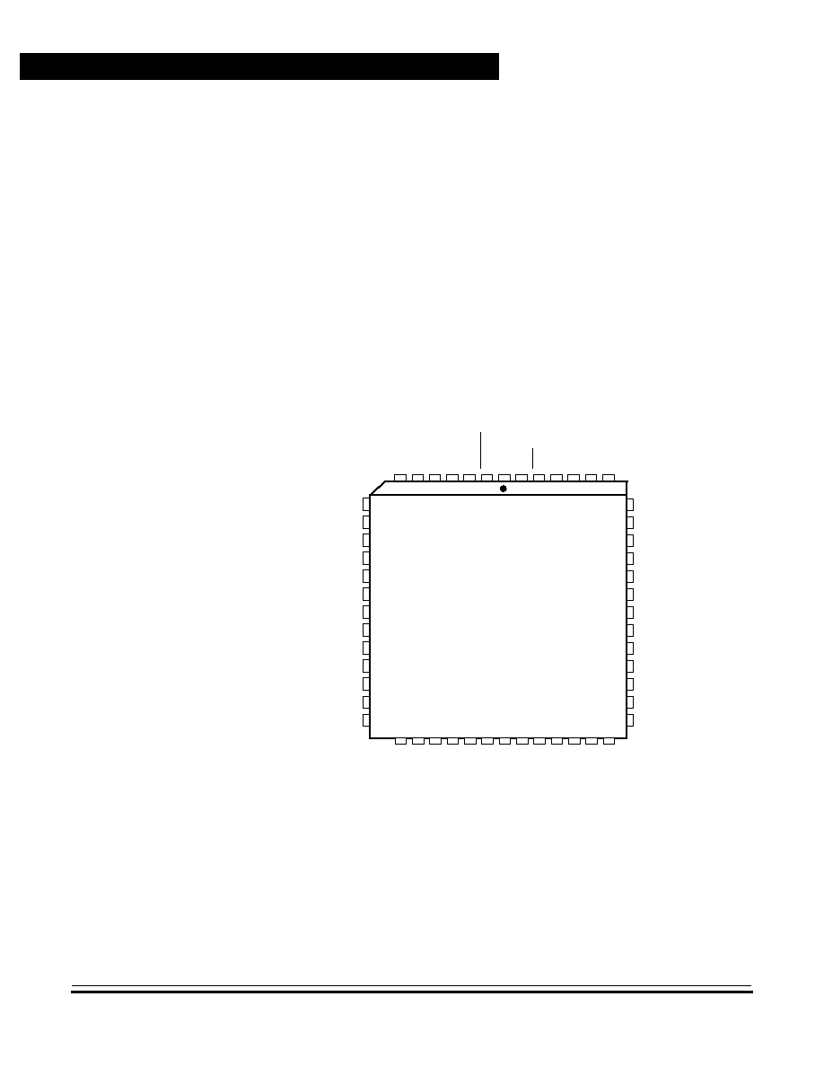
Figure 1-2 shows the PLCC pin assignments.
Figure 1-2. MC68HC(7)05H12 Pin Assignments
(52-pin PLCC package)
40
46
8
14
21
27
7
1
47
34
20
33
VREFH
AVDD
VDD
PC0/TCAP0
PC1/TCAP1
PC2/TCAP2
PC3/TCAP3
PC4/TCMP0
PC5/TCMP1
PC6/RDI
PC7/TDO
PVDD2
PVSS2
PE7
PE6
PE5
PE4
PF3
PF2
PF1
PF0
PE3
PE2
PE1
PE0
PVSS1
PB3
PB2/ECLK
PB1
PB0
PA7
PA6
PA5
PA4
PA3
PA2
PA1
PA0
PVDD1
PD3/AN3
PD2/AN2
PD1/AN1
PD0/AN0
VSS
RESET
OSC1
OSC2
IRQ
/VPP
PB7/SCK
PB6/MOSI
PB5/MISO
PB4

General Description
Functional Pin Description
MC68HC(7)05H12
--
Rev. 1.0
General Release Specification
MOTOROLA
General Description
21
NON-DISCLOSURE AGREEMENT REQUIRED
1.6 Functional Pin Description
The following paragraphs give a description of the general function of
each pin.
1.6.1 VDD and VSS
Power is supplied to the MCU through VDD and VSS. VDD is the
positive supply, and VSS is ground.
1.6.2 AVDD
AVDD is a separate supply pin providing power to the A/D converter.
1.6.3 OSC1, OSC2
The OSC1 and OSC2 pins are the connections for the on-chip oscillator.
A crystal connected across these pins or an external signal connected
to OSC1 provides the oscillator clock. The frequency, f
OSC
, of the
oscillator or external clock source is divided by two or eight (slow mode)
to produce the internal operating frequency, f
OP
.
1.6.4 RESET
This pin can be used as an input to reset the MCU to a known start-up
state by pulling it to the low state. The RESET pin contains an internal
Schmitt trigger to improve its noise immunity as an input. The RESET pin
has an internal pulldown device that pulls the RESET pin low when there
is an internal COP watchdog reset, power-on reset (POR), illegal
address reset, or an internal low voltage reset. Refer to
Section 5 Resets. The RESET pin contains an internal pullup device.
1.6.5 IRQ/VPP
The interrupt triggering sensitivity of this pin can be programmed as
falling edge sensitive or falling edge and low level sensitive.The IRQ pin

NON-DISCLOSURE AGREEMENT REQUIRED
General Description
General Release Specification
MC68HC(7)05H12
--
Rev. 1.0
22
General Description
MOTOROLA
contains an internal Schmitt trigger as part of its input to improve noise
immunity. See Section 4 Interrupts for more details on the interrupts.
IRQ/VPP is also the EPROM programming power pin.
1.6.6 PA0≠PA7/Keyboard Interrupt
These eight I/O lines comprise port A. The state of any pin is software
programmable and all port A lines are configured as inputs during
power-on or reset. The eight I/O lines are shared with the keyboard
interrupt function. See Section 7 Input/Output Ports for more details
on the I/O ports.
1.6.7 PB0≠PB7/ECLK, MISO, MOSI, SCK
These eight I/O lines comprise port B. The state of any pin is software
programmable and all port B lines are configured as inputs during
power-on or reset. See Section 7 Input/Output Ports for more details
on the I/O ports. The port pins PB5≠PB7 are shared with the SPI system
(MISO, MOSI, SCK). See Section 10 Serial Peripheral Interface
(SPI) for more details on the operation of the SPI. Pin PB2 is shared with
the internal system clock ECLK. See Section 2.3.1 System Control
Register.
1.6.8 PC0≠PC7/TCAP0≠3, TCMP0≠1, RDI, TDO
These eight I/O lines comprise port C. The state of any pin is software
programmable and all port C lines are configured as inputs during
power-on or reset. See Section 7 Input/Output Ports for more details
on the I/O ports. The port pins PC0≠PC5 are shared with the 16-bit timer
(TCAP0≠3, TCMP0≠1). See Section 9 16-Bit Timers for more details
on the operation of the 16-bit timers. The port pins PC6 and PC7 are
shared with the SCI system (RDI and TDO). Refer to Section 11 Serial
Communications Interface (SCI).

General Description
Functional Pin Description
MC68HC(7)05H12
--
Rev. 1.0
General Release Specification
MOTOROLA
General Description
23
NON-DISCLOSURE AGREEMENT REQUIRED
1.6.9 PD0≠PD3/AN0≠AN3
These four input only lines comprise port D. See
Section 7 Input/Output Ports for more details on the I/O ports. When
the A/D converter is active, one of the 4 input lines may be selected by
the A/D multiplexer for conversion. See Section 12 Analog to Digital
Converter for more details on the operation of the A/D subsystem.
1.6.10 VREFH
This pin provides the positive reference voltage for the A/D converter.
VSS provides the negative reference voltage for the A/D converter.
1.6.11 PE0≠PE7
These eight output only lines comprise port E. See
Section 7 Input/Output Ports for more details on the I/O ports. The
eight lines are shared with four PWM H-bridge driver pairs. The outputs
are formed by special power drivers. See Section 14 Pulse Width
Modulator (PWM) for more details on the PWM subsystem.
1.6.12 PF0≠PF3
These four output only lines comprise port F. See
Section 7 Input/Output Ports for more details on the I/O ports. The
four lines are shared with four PWM channels. The outputs are formed
by special power drivers. See Section 14 Pulse Width Modulator
(PWM) for more details on the PWM subsystem.
1.6.13 PVDD1, PVSS1, PVDD2, PVSS2
Power is supplied to the power drivers through PVDD and PVSS.
PVDD1 and PVSS1 are the supply pins for PE0≠3 and PF0≠1 and
PVDD2 and PVSS2 are the supply pins for PE4≠7 and PF2≠3.
The VSS pin and the PVSS1 and PVSS2 pins are connected internally.

NON-DISCLOSURE AGREEMENT REQUIRED
General Description
General Release Specification
MC68HC(7)05H12
--
Rev. 1.0
24
General Description
MOTOROLA

MC68HC(7)05H12
--
Rev. 1.0
General Release Specification
MOTOROLA
Memory
25
NON-DISCLOSURE AGREEMENT REQUIRED
General Release Specification -- MC68HC(7)05H12
Section 2. Memory
2.1 Contents
2.2
Introduction . . . . . . . . . . . . . . . . . . . . . . . . . . . . . . . . . . . . . . . . 25
2.3
Registers. . . . . . . . . . . . . . . . . . . . . . . . . . . . . . . . . . . . . . . . . . 26
2.3.1
System Control Register . . . . . . . . . . . . . . . . . . . . . . . . . . . 34
2.4
RAM . . . . . . . . . . . . . . . . . . . . . . . . . . . . . . . . . . . . . . . . . . . . . 35
2.5
ROM . . . . . . . . . . . . . . . . . . . . . . . . . . . . . . . . . . . . . . . . . . . . . 35
2.6
Monitor ROM . . . . . . . . . . . . . . . . . . . . . . . . . . . . . . . . . . . . . . 35
2.7
User EPROM (for the 705 version only) . . . . . . . . . . . . . . . . . . 35
2.8
EEPROM . . . . . . . . . . . . . . . . . . . . . . . . . . . . . . . . . . . . . . . . . 35
2.2 Introduction
The MC68HC(7)05H12 has a 16K byte memory map consisting of
registers (for I/O, control and status), user RAM, user ROM (or EPROM),
EEPROM, monitor ROM, and reset and interrupt vectors as shown in
Figure 2-1.

NON-DISCLOSURE AGREEMENT REQUIRED
Memory
General Release Specification
MC68HC(7)05H12
--
Rev. 1.0
26
Memory
MOTOROLA
2.3 Registers
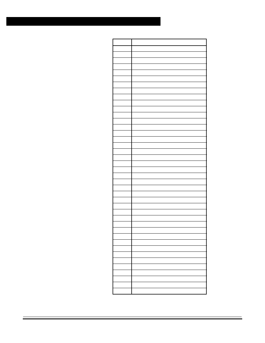
The I/O and control registers reside in locations $0000≠$004F. The
overall organization of these registers is shown in Figure 1-2. The bit
assignments for each register are shown in Figure 2-3, Figure 2-4,
Figure 2-5, Figure 2-6, and Figure 2-7.
$0000
I/O registers
80 bytes
$004F
$0050
User RAM
256 bytes
Stack RAM
64 bytes
$00C0
$00FF
$014F
$0150
Unused
688 bytes
$03FF
$0400
User EEPROM
256 bytes
$04FF
$0500
Unused 2816 bytes
$0FFF
$1000
User ROM
12032 bytes
$3EFF
$3F00
Monitor ROM
240 bytes
$3FEF
$3FF0
User vectors
16 bytes
$3FFF
Figure 2-1. MC68HC(7)05H12 Memory Map

Memory
Registers
MC68HC(7)05H12
--
Rev. 1.0
General Release Specification
MOTOROLA
Memory
27
NON-DISCLOSURE AGREEMENT REQUIRED
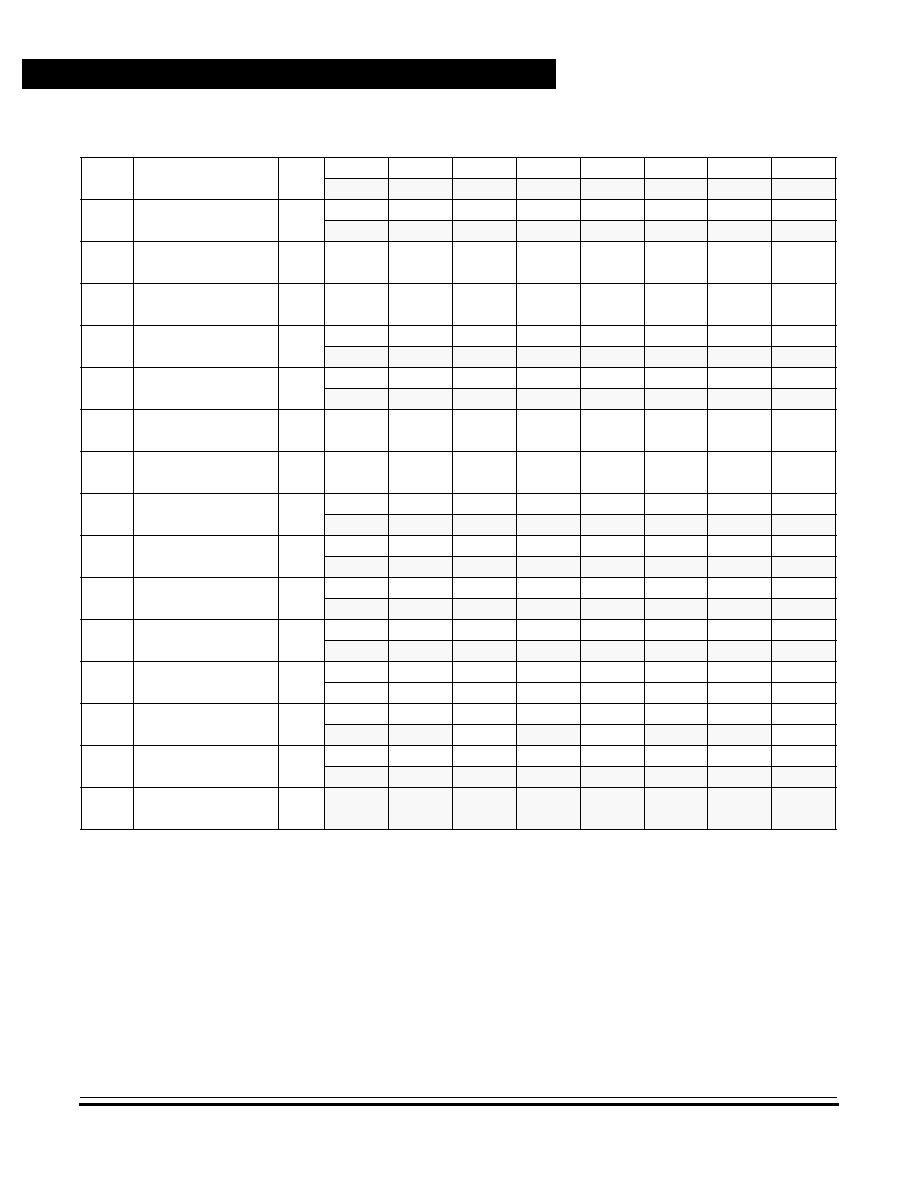
Addr
Register Name
$0000
Port A Data Register
$0001
Port B Data Register
$0002
Port C Data Register
$0003
Port D Data Register
$0004
Port A Data Direction Register
$0005
Port B Data Direction Register
$0006
Port C Data Direction Register
$0007
Port C Control Register
$0008
Core Timer Control/Status (CTCSR)
$0009
Core Timer Counter (CTCR)
$000A
Unused
$000B
Unused
$000C
Unused
$000D
Port A Interrupt Edge
$000E
Port A Interrupt Control
$000F
Port A Interrupt Status
$0010
PWM Data 0
$0011
PWM Data 1
$0012
PWM Data 2
$0013
PWM Data 3
$0014
PWM Data 4
$0015
PWM Data 5
$0016
PWM Data 6
$0017
PWM Data 7
$0018
PWM Control/Sign
$0019
PWM Channel Enable
$001A
PWM Channel Polarity
$001B
Unused
$001C
EEPROM Control
$001D
RESERVED for 705 version
$001E
Unused
$001F
TEST
$0020
Timer1 Capture 1 High
$0021
Timer1 Capture 1 Low
$0022
Timer1 Compare 1 High
$0023
Timer1 Compare 1 Low
$0024
Timer1 Capture 2 High
$0025
Timer1 Capture 2 Low
$0026
Timer1 Compare 2 High
Figure 2-2. I/O Register Summary
NON-DISCLOSURE AGREEMENT REQUIRED
Memory
General Release Specification
MC68HC(7)05H12
--
Rev. 1.0
28
Memory
MOTOROLA
$0027
Timer1 Compare 2 Low
$0028
Timer1 Counter High
$0029
Timer1 Counter Low
$002A
Timer1 Alternate Counter High
$002B
Timer1 Alternate Counter Low
$002C
Timer1 Control 1
$002D
Timer1 Control 2
$002E
Timer1 Status
$002F
Unused
$0030
Timer2 Capture 1 High
$0031
Timer2 Capture 1 Low
$0032
Timer2 Compare 1 High
$0033
Timer2 Compare 1 Low
$0034
Timer2 Capture 2 High
$0035
Timer2 Capture 2 Low
$0036
Timer2 Compare 2 High
$0037
Timer2 Compare 2 Low
$0038
Timer2 Counter High
$0039
Timer2 Counter Low
$003A
Timer2 Alternate Counter High
$003B
Timer2 Alternate Counter Low
$003C
Timer2 Control 1
$003D
Timer2 Control 2
$003E
Timer2 Status
$003F
Unused
$0040
Port E Data Register
$0041
Port E Mismatch Register
$0042
Port F Data Register
$0043
Port F Mismatch Register
$0044
SPI Control
$0045
SPI Status
$0046
SPI Data I/O
$0047
SCI SCDAT
$0048
SCI SCCR1
$0049
SCI SCCR2
$004A
SCI SCSR
$004B
SCI BAUD
$004C
Unused
$004D
System Control Register
$004E
A/D DATA
$004F
A/D STATUS/CTL
Addr
Register Name
Figure 2-2. I/O Register Summary

Memory
Registers
MC68HC(7)05H12
--
Rev. 1.0
General Release Specification
MOTOROLA
Memory
29
NON-DISCLOSURE AGREEMENT REQUIRED
Addr
Register
R/W
Bit 7
Bit 6
Bit 5
Bit 4
Bit 3
Bit 2
Bit 1
Bit 0
$0000
Port A Data
R
PA7
PA6
PA5
PA4
PA3
PA2
PA1
PA0
W
$0001
Port B Data
R
PB7
PB6
PB5
PB4
PB3
PB2
PB1
PB0
W
$0002
Port C Data
R
PC7
PC6
PC5
PC4
PC3
PC2
PC1
PC0
W
$0003
Port D Data
R
0
0
0
0
PD3
PD2
PD1
PD0
W
$0004
Port A Data Direction
R
DDRA7
DDRA6
DDRA5
DDRA4
DDRA3
DDRA2
DDRA1
DDRA0
W
$0005
Port B Data Direction
R
DDRB7
DDRB6
DDRB5
DDRB4
DDRB3
DDRB2
DDRB1
DDRB0
W
$0006
Port C Data Direction
R
DDRC7
DDRC6
DDRC5
DDRC4
DDRC3
DDRC2
DDRC1
DDRC0
W
$0007
Port C Control
R
0
0
TCMP1
TCMP0
0
0
0
0
W
$0008
CTSCR
R
TOF
RTIF
TOFE
RTIE
0
0
RT1
RT0
W
RTOF
RTIF
$0009
CTCR
R
bit 7
bit 6
bit 5
bit 4
bit 3
bit 2
bit 1
bit 0
W
$000A
Unimplemented
R
W
$000B
Unimplemented
R
W
$000C
Unimplemented
R
W
$000D
PAIED
R
EDGE7
EDGE6
EDGE5
EDGE4
EDGE3
EDGE2
EDGE1
EDGE0
W
$000E
PAICR
R
PAIE7
PAIE6
PAIE5
PAIE4
PAIE3
PAIE2
PAIE1
PAIE0
W
$000F
PAISR
R
PAIF7
PAIF6
PAIF5
PAIF4
PAIF3
PAIF2
PAIF1
PAIF0
W
Figure 2-3. I/O Registers $0000≠$000F

NON-DISCLOSURE AGREEMENT REQUIRED
Memory
General Release Specification
MC68HC(7)05H12
--
Rev. 1.0
30
Memory
MOTOROLA
Addr
Register
R/W
Bit 7
Bit 6
Bit 5
Bit 4
Bit 3
Bit 2
Bit 1
Bit 0
$0010
PWM Data 0
R
bit 7
bit 6
bit 5
bit 4
bit 3
bit 2
bit 1
bit 0
W
$0011
PWM Data 1
R
bit 7
bit 6
bit 5
bit 4
bit 3
bit 2
bit 1
bit 0
W
$0012
PWM Data 2
R
bit 7
bit 6
bit 5
bit 4
bit 3
bit 2
bit 1
bit 0
W
$0013
PWM Data 3
R
bit 7
bit 6
bit 5
bit 4
bit 3
bit 2
bit 1
bit 0
W
$0014
PWM Data 4
R
bit 7
bit 6
bit 5
bit 4
bit 3
bit 2
bit 1
bit 0
W
$0015
PWM Data 5
R
bit 7
bit 6
bit 5
bit 4
bit 3
bit 2
bit 1
bit 0
W
$0016
PWM Data 6
R
bit 7
bit 6
bit 5
bit 4
bit 3
bit 2
bit 1
bit 0
W
$0017
PWM Data 7
R
bit 7
bit 6
bit 5
bit 4
bit 3
bit 2
bit 1
bit 0
W
$0018
PWMCTL
R
0
PWMC3
PWMC2
PWMC1
SIGN3
SIGN2
SIGN1
SIGN0
W
PWMRS
$0019
PWMEN
R
PWME7
PWME6
PWME5
PWME4
PWME3
PWME2
PWME1
PWME0
W
$001A
PWMPOL
R
PPOL7
PPOL6
PPOL5
PPOL4
PPOL3
PPOL2
PPOL1
PPOL0
W
$001B
Unimplemented
R
W
$001C
EEPCR
R
0
0
0
EEOSC
ER1
EER0
EELAT
EEPGM
W
$001D
Reserved for 705 ver-
sion
R
W
$001E
Unimplemented
R
W
$001F
TEST
R
0
0
0
0
0
0
0
0
W
Figure 2-4. I/O Registers $0010≠$001F

Memory
Registers
MC68HC(7)05H12
--
Rev. 1.0
General Release Specification
MOTOROLA
Memory
31
NON-DISCLOSURE AGREEMENT REQUIRED
Addr
Register
R/W
Bit 7
Bit 6
Bit 5
Bit 4
Bit 3
Bit 2
Bit 1
Bit 0
$0020
Timer 1 Input
Capture1 High
R
bit 15
bit 14
bit 13
bit 12
bit 11
bit 10
bit 9
bit 8
W
$0021
Timer 1 Input
Capture1 Low
R
bit 7
bit 6
bit 5
bit 4
bit 3
bit 2
bit 1
bit 0
W
$0022
Timer 1 Output
Compare1 High
R
bit 15
bit 14
bit 13
bit 12
bit 11
bit 10
bit 9
bit 8
W
$0023
Timer 1 Output
Compare1 Low
R
bit 7
bit 6
bit 5
bit 4
bit 3
bit 2
bit 1
bit 0
W
$0024
Timer 1 Input
Capture2 High
R
bit 15
bit 14
bit 13
bit 12
bit 11
bit 10
bit 9
bit 8
W
$0025
Timer 1 Input
Capture2 Low
R
bit 7
bit 6
bit 5
bit 4
bit 3
bit 2
bit 1
bit 0
W
$0026
Timer 1 Output
Compare2 High
R
bit 15
bit 14
bit 13
bit 12
bit 11
bit 10
bit 9
bit 8
W
$0027
Timer 1 Output
Compare2 Low
R
bit 7
bit 6
bit 5
bit 4
bit 3
bit 2
bit 1
bit 0
W
$0028
Timer 1 Counter High
R
bit 15
bit 14
bit 13
bit 12
bit 11
bit 10
bit 9
bit 8
W
$0029
Timer 1 Counter Low
R
bit 7
bit 6
bit 5
bit 4
bit 3
bit 2
bit 1
bit 0
W
$002A
Timer 1 Alternate
Counter High
R
bit 15
bit 14
bit 13
bit 12
bit 11
bit 10
bit 9
bit 8
W
$002B
Timer 1 Alternate
Counter Low
R
bit 7
bit 6
bit 5
bit 4
bit 3
bit 2
bit 1
bit 0
W
$002C
Timer 1 Control 1
R
ICI1E
ICI2E
OCI1E
TOIE
CO1E
IEDG1
IEDG2
OLVL1
W
$002D
Timer 1 Control 2
R
0
0
OC2IE
0
CO2E
0
0
OLVL2
W
$002E
Timer 1 Status
R
IC1F
IC2F
OC1F
TOF
TCAP1
TCAP2
OC2F
0
W
$002F
Unimplemented
R
W
Figure 2-5. I/O Registers $0020≠$002F
NON-DISCLOSURE AGREEMENT REQUIRED
Memory
General Release Specification
MC68HC(7)05H12
--
Rev. 1.0
32
Memory
MOTOROLA
Addr
Register
R/W
Bit 7
Bit 6
Bit 5
Bit 4
Bit 3
Bit 2
Bit 1
Bit 0
$0030
Timer 2 Input Capture1
High
R
bit 15
bit 14
bit 13
bit 12
bit 11
bit 10
bit 9
bit 8
W
$0031
Timer 2 Input Capture1
Low
R
bit 7
bit 6
bit 5
bit 4
bit 3
bit 2
bit 1
bit 0
W
$0032
Timer 2 Output
Compare1 High
R
bit 15
bit 14
bit 13
bit 12
bit 11
bit 10
bit 9
bit 8
W
$0033
Timer 2 Output
Compare1 Low
R
bit 7
bit 6
bit 5
bit 4
bit 3
bit 2
bit 1
bit 0
W
$0034
Timer 2 Input Capture2
High
R
bit 15
bit 14
bit 13
bit 12
bit 11
bit 10
bit 9
bit 8
W
$0035
Timer 2 Input Capture2
Low
R
bit 7
bit 6
bit 5
bit 4
bit 3
bit 2
bit 1
bit 0
W
$0036
Timer 2 Output
Compare2 High
R
bit 15
bit 14
bit 13
bit 12
bit 11
bit 10
bit 9
bit 8
W
$0037
Timer 2 Output
Compare2 Low
R
bit 7
bit 6
bit 5
bit 4
bit 3
bit 2
bit 1
bit 0
W
$0038
Timer 2 Counter High
R
bit 15
bit 14
bit 13
bit 12
bit 11
bit 10
bit 9
bit 8
W
$0039
Timer 2 Counter Low
R
bit 7
bit 6
bit 5
bit 4
bit 3
bit 2
bit 1
bit 0
W
$003A
Timer 2 Alternate
Counter High
R
bit 15
bit 14
bit 13
bit 12
bit 11
bit 10
bit 9
bit 8
W
$003B
Timer 2 Alternate
Counter Low
R
bit 7
bit 6
bit 5
bit 4
bit 3
bit 2
bit 1
bit 0
W
$003C
Timer 2 Control 1
R
ICI1E
ICI2E
OCI1E
TOIE
CO1E
IEDG1
IEDG2
OLVL1
W
$003D
Timer 2 Control 2
R
0
0
OC2IE
0
CO2E
0
0
OLVL2
W
$003E
Timer 2 Status
R
IC1F
IC2F
OC1F
TOF
TCAP1
TCAP2
OC2F
0
W
$003F
Unimplemented
R
W
Figure 2-6. I/O Registers $0030≠$003F

Memory
Registers
MC68HC(7)05H12
--
Rev. 1.0
General Release Specification
MOTOROLA
Memory
33
NON-DISCLOSURE AGREEMENT REQUIRED
Addr
Register
R/W
Bit 7
Bit 6
Bit 5
Bit 4
Bit 3
Bit 2
Bit 1
Bit 0
$0040
Port E Data
R
PE7
PE6
PE5
PE4
PE3
PE2
PE1
PE0
W
$0041
Port E Mismatch
R
bit 7
bit 6
bit 5
bit 4
bit 3
bit 2
bit 1
bit 0
W
$0042
Port F Data
R
0
0
0
0
PF3
PF2
PF1
PF0
W
$0043
Port F Mismatch
R
0
0
0
0
bit 3
bit 2
bit 1
bit 0
W
$0044
SPI Control
R
SPIE
SPE
DOD
MSTR
CPOL
CPHA
SPR1
SPR0
W
$0045
SPI Status
R
SPIF
WCOL
0
0
0
0
0
0
W
$0046
SPI Data
R
bit 7
bit 6
bit 5
bit 4
bit 3
bit 2
bit 1
bit 0
W
$0047
SCI Data
R
bit 7
bit 6
bit 5
bit 4
bit 3
bit 2
bit 1
bit 0
W
$0048
SCI Control 1
R
R8
T8
0
M
WAKE
0
0
0
W
$0049
SCI Control 2
R
TIE
TCIE
RIE
ILIE
TE
RE
RWU
SBK
W
$004A
SCI Status
R
TDRE
TC
RDRF
IDLE
OR
NF
FE
0
W
$004B
SCI BAUD
R
0
SPP
SCP1
SCP0
0
SCR2
SCR1
SCR0
W
TCLR
RCKB
$004C
Unimplemented
R
W
$004D
System Control
R
0
0
0
SC
IRQ
0
0
ECLK
W
$004E
A/D Data
R
bit 7
bit 6
bit 5
bit 4
bit 3
bit 2
bit 1
bit 0
W
$004F
A/D Status/Control
R
COCO
ADRC
ADON
0
CH3
CH2
CH1
CH0
W
Figure 2-7. I/O Registers $0040≠$004F

NON-DISCLOSURE AGREEMENT REQUIRED
Memory
General Release Specification
MC68HC(7)05H12
--
Rev. 1.0
34
Memory
MOTOROLA
2.3.1 System Control Register
The MC68HC(7)05H12 contains a system control register which is
located at $004D. This register is used to control the IRQ interrupt
sensitivity, the bus frequency, and the external availability of the internal
bus clock.
SC -- System Clock Option
After power on reset the internal bus frequency f
OP
is = f
OSC
/2. The
SC bit allows the user to reduce the system speed to f
OSC
/8.
1 = f
OP
= f
OSC
/8 (Slow Mode)
0 = f
OP
= f
OSC
/2
IRQ -- IRQ Sensitivity
IRQ edge or level sensitive
1 = IRQ input edge and level sensitive
0 = IRQ input edge sensitive
ECLK -- Internal System Clock Available
The ECLK bit makes the internal system clock (bus frequency f
OP
)
available to the user. Refer to Section 7.4 Port B for more details.
1 = The PB2/ECLK pin provides the internal system clock
independently of the value of the port B data direction register
0 = The internal system clock is not available, the PB2/ECLK pin is
an ordinary I/O port line
$004D
Bit 7
6
5
4
3
2
1
Bit 0
Read:
0
0
0
SC
IRQ
0
0
ECLK
Write:
Reset:
0
0
0
0
0
0
0
0
Figure 2-8. System Control Register (SYSCR)

Memory
RAM
MC68HC(7)05H12
--
Rev. 1.0
General Release Specification
MOTOROLA
Memory
35
NON-DISCLOSURE AGREEMENT REQUIRED
2.4 RAM
The user RAM consists of 256 bytes ranging from $0050 to $014F. The
stack begins at address $00FF. The stack pointer can access 64 bytes
of RAM in the range $00FF to $00C0.
The stack is located in the middle of the RAM address space. Data
written to addresses within the stack address range could be overwritten
during stack activity.
2.5 ROM
The 12032 bytes of the user ROM are located from $1000 to $3EFF, plus
16 bytes of user vectors from $3FF0 to $3FFF.
2.6 Monitor ROM
The monitor ROM ranges from $3F00 to $3FEF. The vectors for the
bootloader are located from $3FE0 to $3FEF.
2.7 User EPROM (for the 705 version only)
The 12032 bytes of the user EPROM are located from $1000 to $3EFD,
including two bytes of mask option registers (MOR) at $3EFE and
$3EFF, plus 16 bytes of user vectors from $3FF0 to $3FFF. Refer to
Section 15 EPROM for programming details.
2.8 EEPROM
This device contains 256 bytes of EEPROM. Programming the
EEPROM is performed by the user on a single-byte basis by
manipulating the EEPROM control register, located at address $001C.
Refer to Section 13 EEPROM for programming details.

NON-DISCLOSURE AGREEMENT REQUIRED
Memory
General Release Specification
MC68HC(7)05H12
--
Rev. 1.0
36
Memory
MOTOROLA

MC68HC(7)05H12
--
Rev. 1.0
General Release Specification
MOTOROLA
CPU and Instruction Set
37
NON-DISCLOSURE AGREEMENT REQUIRED
General Release Specification -- MC68HC(7)05H12
Section 3. CPU and Instruction Set
3.1 Contents
3.2
Introduction . . . . . . . . . . . . . . . . . . . . . . . . . . . . . . . . . . . . . . . . 38
3.3
CPU Registers . . . . . . . . . . . . . . . . . . . . . . . . . . . . . . . . . . . . . 38
3.3.1
Accumulator . . . . . . . . . . . . . . . . . . . . . . . . . . . . . . . . . . . . 39
3.3.2
Index Register . . . . . . . . . . . . . . . . . . . . . . . . . . . . . . . . . . . 39
3.3.3
Stack Pointer . . . . . . . . . . . . . . . . . . . . . . . . . . . . . . . . . . . . 39
3.3.4
Program Counter. . . . . . . . . . . . . . . . . . . . . . . . . . . . . . . . . 40
3.3.5
Condition Code Register . . . . . . . . . . . . . . . . . . . . . . . . . . . 40
3.4
Arithmetic/Logic Unit (ALU) . . . . . . . . . . . . . . . . . . . . . . . . . . . 42
3.5
Instruction Set Overview. . . . . . . . . . . . . . . . . . . . . . . . . . . . . . 42
3.6
Addressing Modes . . . . . . . . . . . . . . . . . . . . . . . . . . . . . . . . . . 42
3.6.1
Inherent . . . . . . . . . . . . . . . . . . . . . . . . . . . . . . . . . . . . . . . . 43
3.6.2
Immediate . . . . . . . . . . . . . . . . . . . . . . . . . . . . . . . . . . . . . . 43
3.6.3
Direct . . . . . . . . . . . . . . . . . . . . . . . . . . . . . . . . . . . . . . . . . . 43
3.6.4
Extended . . . . . . . . . . . . . . . . . . . . . . . . . . . . . . . . . . . . . . . 43
3.6.5
Indexed, No Offset . . . . . . . . . . . . . . . . . . . . . . . . . . . . . . . 44
3.6.6
Indexed, 8-Bit Offset . . . . . . . . . . . . . . . . . . . . . . . . . . . . . . 44
3.6.7
Indexed,16-Bit Offset. . . . . . . . . . . . . . . . . . . . . . . . . . . . . . 44
3.6.8
Relative . . . . . . . . . . . . . . . . . . . . . . . . . . . . . . . . . . . . . . . . 45
3.7
Instruction Types . . . . . . . . . . . . . . . . . . . . . . . . . . . . . . . . . . . 45
3.7.1
Register/Memory Instructions . . . . . . . . . . . . . . . . . . . . . . . 46
3.7.2
Read-Modify-Write Instructions . . . . . . . . . . . . . . . . . . . . . . 47
3.7.3
Jump/Branch Instructions . . . . . . . . . . . . . . . . . . . . . . . . . . 48
3.7.4
Bit Manipulation Instructions . . . . . . . . . . . . . . . . . . . . . . . . 50
3.7.5
Control Instructions . . . . . . . . . . . . . . . . . . . . . . . . . . . . . . . 51
3.8
Instruction Set Summary . . . . . . . . . . . . . . . . . . . . . . . . . . . . . 52

NON-DISCLOSURE AGREEMENT REQUIRED
CPU and Instruction Set
General Release Specification
MC68HC(7)05H12
--
Rev. 1.0
38
CPU and Instruction Set
MOTOROLA
3.2 Introduction
This chapter describes the CPU registers and the HC05 instruction set.
3.3 CPU Registers
Figure 3-1 shows the five CPU registers. CPU registers are not part of
the memory map.
Figure 3-1. Programming Model
ACCUMULATOR (A)
A
INDEX REGISTER (X)
X
SP
1
1
0
0
0
0
0
0
0
0
PCL
PCH
Z
C
I
N
1
H
1
1
0
4
7
5
CONDITION CODE REGISTER (CCR)
PROGRAM COUNTER (PC)
STACK POINTER (SP)
0
7
8
15
15
5
7
7
0
0
0
HALF-CARRY FLAG
INTERRUPT MASK
NEGATIVE FLAG
ZERO FLAG
CARRY/BORROW FLAG
10
6

CPU and Instruction Set
CPU Registers
MC68HC(7)05H12
--
Rev. 1.0
General Release Specification
MOTOROLA
CPU and Instruction Set
39
NON-DISCLOSURE AGREEMENT REQUIRED
3.3.1 Accumulator
The accumulator is a general-purpose 8-bit register. The CPU uses the
accumulator to hold operands and results of arithmetic and non-
arithmetic operations.
3.3.2 Index Register
In the indexed addressing modes, the CPU uses the byte in the index
register to determine the conditional address of the operand.
The 8-bit index register can also serve as a temporary data storage
location.
3.3.3 Stack Pointer
The stack pointer is a 16-bit register that contains the address of the next
location on the stack. During a reset or after the reset stack pointer
(RSP) instruction, the stack pointer is preset to $00FF. The address in
the stack pointer decrements as data is pushed onto the stack and
increments as data is pulled from the stack.
Bit 7
6
5
4
3
2
1
Bit 0
Reset:
Unaffected by reset
Figure 3-2. Accumulator
Bit 7
6
5
4
3
2
1
Bit 0
Reset:
Unaffected by reset
Figure 3-3. Index Register
Bit 15 14
13
12
11
10
9
8
7
6
5
4
3
2
1
Bit 0
0
0
0
0
0
0
0
0
1
1
Reset
0
0
0
0
0
0
0
0
1
1
1
1
1
1
1
1
Figure 3-4. Stack Pointer

NON-DISCLOSURE AGREEMENT REQUIRED
CPU and Instruction Set
General Release Specification
MC68HC(7)05H12
--
Rev. 1.0
40
CPU and Instruction Set
MOTOROLA
The ten most significant bits of the stack pointer are permanently fixed
at 000000011, so the stack pointer produces addresses from $00C0 to
$00FF. If subroutines and interrupts use more than 64 stack locations,
the stack pointer wraps around to address $00FF and begins writing
over the previously stored data. A subroutine uses two stack locations.
An interrupt uses five locations.
3.3.4 Program Counter
The program counter is a 16-bit register that contains the address of the
next instruction or operand to be fetched. The two most significant bits
of the program counter are ignored internally.
Normally, the address in the program counter automatically increments
to the next sequential memory location every time an instruction or
operand is fetched. Jump, branch, and interrupt operations load the
program counter with an address other than that of the next sequential
location.
3.3.5 Condition Code Register
The condition code register is an 8-bit register whose three most
significant bits are permanently fixed at 111. The condition code register
contains the interrupt mask and four flags that indicate the results of the
instruction just executed. The following paragraphs describe the
functions of the condition code register.
Bit 15 14
13
12
11
10
9
8
7
6
5
4
3
2
1
Bit 0
≠
≠
Reset
≠
≠
Loaded with vector from $3FFE AND $3FFF
Figure 3-5. Program Counter
Bit 7
6
5
4
3
2
1
Bit 0
1
1
1
H
I
N
C
Z
Reset
1
1
1
U
1
U
U
U
Figure 3-6. Condition Code Register

CPU and Instruction Set
CPU Registers
MC68HC(7)05H12
--
Rev. 1.0
General Release Specification
MOTOROLA
CPU and Instruction Set
41
NON-DISCLOSURE AGREEMENT REQUIRED
Half-Carry Flag
The CPU sets the half-carry flag when a carry occurs between bits 3 and
4 of the accumulator during an ADD or ADC operation. The half-carry
flag is required for binary-coded decimal (BCD) arithmetic operations.
Interrupt Mask
Setting the interrupt mask disables interrupts. If an interrupt request
occurs while the interrupt mask is logic zero, the CPU saves the CPU
registers on the stack, sets the interrupt mask, and then fetches the
interrupt vector. If an interrupt request occurs while the interrupt mask is
set, the interrupt request is latched. Normally, the CPU processes the
latched interrupt as soon as the interrupt mask is cleared again.
A return from interrupt (RTI) instruction pulls the CPU registers from the
stack, restoring the interrupt mask to its cleared state. After any reset,
the interrupt mask is set and can be cleared only by a software
instruction.
Negative Flag
The CPU sets the negative flag when an arithmetic operation, logical
operation, or data manipulation produces a negative result.
Zero Flag
The CPU sets the zero flag when an arithmetic operation, logical
operation, or data manipulation produces a result of $00.
Carry/Borrow Flag
The CPU sets the carry/borrow flag when an addition operation
produces a carry out of bit 7 of the accumulator or when a subtraction
operation requires a borrow. Some logical operations and data
manipulation instructions also clear or set the carry/borrow flag.

NON-DISCLOSURE AGREEMENT REQUIRED
CPU and Instruction Set
General Release Specification
MC68HC(7)05H12
--
Rev. 1.0
42
CPU and Instruction Set
MOTOROLA
3.4 Arithmetic/Logic Unit (ALU)
The ALU performs the arithmetic and logical operations defined by the
instruction set.
The binary arithmetic circuits decode instructions and set up the ALU for
the selected operation. Most binary arithmetic is based on the addition
algorithm, carrying out subtraction as negative addition. Multiplication is
not performed as a discrete operation but as a chain of addition and shift
operations within the ALU. The multiply instruction (MUL) requires 11
internal clock cycles to complete this chain of operations.
3.5 Instruction Set Overview
The MCU instruction set has 62 instructions and uses eight addressing
modes. The instructions include all those of the M146805 CMOS Family
plus one more: the unsigned multiply (MUL) instruction. The MUL
instruction allows unsigned multiplication of the contents of the
accumulator (A) and the index register (X). The high-order product is
stored in the index register, and the low-order product is stored in the
accumulator.
3.6 Addressing Modes
The CPU uses eight addressing modes for flexibility in accessing data.
The addressing modes provide eight different ways for the CPU to find
the data required to execute an instruction. The eight addressing modes
are:
∑
Inherent
∑
Immediate
∑
Direct
∑
Extended
∑
Indexed, no offset
∑
Indexed, 8-bit offset

CPU and Instruction Set
Addressing Modes
MC68HC(7)05H12
--
Rev. 1.0
General Release Specification
MOTOROLA
CPU and Instruction Set
43
NON-DISCLOSURE AGREEMENT REQUIRED
∑
Indexed, 16-bit offset
∑
Relative
3.6.1 Inherent
Inherent instructions are those that have no operand, such as return
from interrupt (RTI). Some of the inherent instructions act on data in the
CPU registers, such as set carry flag (SEC) and increment accumulator
(INCA). Inherent instructions require no operand address and are one
byte long.
3.6.2 Immediate
Immediate instructions are those that contain a value to be used in an
operation with the value in the accumulator or index register. Immediate
instructions require no operand address and are two bytes long. The
opcode is the first byte, and the immediate data value is the second byte.
3.6.3 Direct
Direct instructions can access any of the first 256 memory locations with
two bytes. The first byte is the opcode, and the second is the low byte of
the operand address. In direct addressing, the CPU automatically uses
$00 as the high byte of the operand address.
3.6.4 Extended
Extended instructions use three bytes and can access any address in
memory. The first byte is the opcode; the second and third bytes are the
high and low bytes of the operand address.
When using the Motorola assembler, the programmer does not need to
specify whether an instruction is direct or extended. The assembler
automatically selects the shortest form of the instruction.

NON-DISCLOSURE AGREEMENT REQUIRED
CPU and Instruction Set
General Release Specification
MC68HC(7)05H12
--
Rev. 1.0
44
CPU and Instruction Set
MOTOROLA
3.6.5 Indexed, No Offset
Indexed instructions with no offset are 1-byte instructions that can
access data with variable addresses within the first 256 memory
locations. The index register contains the low byte of the effective
address of the operand. The CPU automatically uses $00 as the high
byte, so these instructions can address locations $0000≠$00FF.
Indexed, no offset instructions are often used to move a pointer through
a table or to hold the address of a frequently used RAM or I/O location.
3.6.6 Indexed, 8-Bit Offset
Indexed, 8-bit offset instructions are 2-byte instructions that can access
data with variable addresses within the first 511 memory locations. The
CPU adds the unsigned byte in the index register to the unsigned byte
following the opcode. The sum is the effective address of the operand.
These instructions can access locations $0000≠$01FE.
Indexed 8-bit offset instructions are useful for selecting the kth element
in an n-element table. The table can begin anywhere within the first 256
memory locations and could extend as far as location 510 ($01FE). The
k value is typically in the index register, and the address of the beginning
of the table is in the byte following the opcode.
3.6.7 Indexed,16-Bit Offset
Indexed, 16-bit offset instructions are 3-byte instructions that can access
data with variable addresses at any location in memory. The CPU adds
the unsigned byte in the index register to the two unsigned bytes
following the opcode. The sum is the effective address of the operand.
The first byte after the opcode is the high byte of the 16-bit offset; the
second byte is the low byte of the offset.
Indexed, 16-bit offset instructions are useful for selecting the kth element
in an n-element table anywhere in memory.
As with direct and extended addressing, the Motorola assembler
determines the shortest form of indexed addressing.

CPU and Instruction Set
Instruction Types
MC68HC(7)05H12
--
Rev. 1.0
General Release Specification
MOTOROLA
CPU and Instruction Set
45
NON-DISCLOSURE AGREEMENT REQUIRED
3.6.8 Relative
Relative addressing is only for branch instructions. If the branch
condition is true, the CPU finds the effective branch destination by
adding the signed byte following the opcode to the contents of the
program counter. If the branch condition is not true, the CPU goes to the
next instruction. The offset is a signed, two's complement byte that gives
a branching range of ≠128 to +127 bytes from the address of the next
location after the branch instruction.
When using the Motorola assembler, the programmer does not need to
calculate the offset, because the assembler determines the proper offset
and verifies that it is within the span of the branch.
3.7 Instruction Types
The MCU instructions fall into the following five categories:
∑
Register/Memory Instructions
∑
Read-Modify-Write Instructions
∑
Jump/Branch Instructions
∑
Bit Manipulation Instructions
∑
Control Instructions

NON-DISCLOSURE AGREEMENT REQUIRED
CPU and Instruction Set
General Release Specification
MC68HC(7)05H12
--
Rev. 1.0
46
CPU and Instruction Set
MOTOROLA
3.7.1 Register/Memory Instructions
These instructions operate on CPU registers and memory locations.
Most of them use two operands. One operand is in either the
accumulator or the index register. The CPU finds the other operand in
memory.
Table 3-1. Register/Memory Instructions
Instruction
Mnemonic
Add Memory Byte and Carry Bit to Accumulator
ADC
Add Memory Byte to Accumulator
ADD
AND Memory Byte with Accumulator
AND
Bit Test Accumulator
BIT
Compare Accumulator
CMP
Compare Index Register with Memory Byte
CPX
EXCLUSIVE OR Accumulator with Memory Byte
EOR
Load Accumulator with Memory Byte
LDA
Load Index Register with Memory Byte
LDX
Multiply
MUL
OR Accumulator with Memory Byte
ORA
Subtract Memory Byte and Carry Bit from Accumulator
SBC
Store Accumulator in Memory
STA
Store Index Register in Memory
STX
Subtract Memory Byte from Accumulator
SUB

CPU and Instruction Set
Instruction Types
MC68HC(7)05H12
--
Rev. 1.0
General Release Specification
MOTOROLA
CPU and Instruction Set
47
NON-DISCLOSURE AGREEMENT REQUIRED
3.7.2 Read-Modify-Write Instructions
These instructions read a memory location or a register, modify its
contents, and write the modified value back to the memory location or to
the register.
NOTE:
Do not use read-modify-write operations on write-only registers.
1. Unlike other read-modify-write instructions, BCLR and
BSET use only direct addressing.
2. TST is an exception to the read-modify-write sequence be-
cause it does not write a replacement value.
Table 3-2. Read-Modify-Write Instructions
Instruction
Mnemonic
Arithmetic Shift Left (Same as LSL)
ASL
Arithmetic Shift Right
ASR
Bit Clear
BCLR
(1)
Bit Set
BSET
(1)
Clear Register
CLR
Complement (One's Complement)
COM
Decrement
DEC
Increment
INC
Logical Shift Left (Same as ASL)
LSL
Logical Shift Right
LSR
Negate (Two's Complement)
NEG
Rotate Left through Carry Bit
ROL
Rotate Right through Carry Bit
ROR
Test for Negative or Zero
TST
(2)

NON-DISCLOSURE AGREEMENT REQUIRED
CPU and Instruction Set
General Release Specification
MC68HC(7)05H12
--
Rev. 1.0
48
CPU and Instruction Set
MOTOROLA
3.7.3 Jump/Branch Instructions
Jump instructions allow the CPU to interrupt the normal sequence of the
program counter. The unconditional jump instruction (JMP) and the
jump-to-subroutine instruction (JSR) have no register operand. Branch
instructions allow the CPU to interrupt the normal sequence of the
program counter when a test condition is met. If the test condition is not
met, the branch is not performed.
The BRCLR and BRSET instructions cause a branch based on the state
of any readable bit in the first 256 memory locations. These 3-byte
instructions use a combination of direct addressing and relative
addressing. The direct address of the byte to be tested is in the byte
following the opcode. The third byte is the signed offset byte. The CPU
finds the effective branch destination by adding the third byte to the
program counter if the specified bit tests true. The bit to be tested and its
condition (set or clear) is part of the opcode. The span of branching is
from ≠128 to +127 from the address of the next location after the branch
instruction. The CPU also transfers the tested bit to the carry/borrow bit
of the condition code register.

CPU and Instruction Set
Instruction Types
MC68HC(7)05H12
--
Rev. 1.0
General Release Specification
MOTOROLA
CPU and Instruction Set
49
NON-DISCLOSURE AGREEMENT REQUIRED
Table 3-3. Jump and Branch Instructions
Instruction
Mnemonic
Branch if Carry Bit Clear
BCC
Branch if Carry Bit Set
BCS
Branch if Equal
BEQ
Branch if Half-Carry Bit Clear
BHCC
Branch if Half-Carry Bit Set
BHCS
Branch if Higher
BHI
Branch if Higher or Same
BHS
Branch if IRQ Pin High
BIH
Branch if IRQ Pin Low
BIL
Branch if Lower
BLO
Branch if Lower or Same
BLS
Branch if Interrupt Mask Clear
BMC
Branch if Minus
BMI
Branch if Interrupt Mask Set
BMS
Branch if Not Equal
BNE
Branch if Plus
BPL
Branch Always
BRA
Branch if Bit Clear
BRCLR
Branch Never
BRN
Branch if Bit Set
BRSET
Branch to Subroutine
BSR
Unconditional Jump
JMP
Jump to Subroutine
JSR

NON-DISCLOSURE AGREEMENT REQUIRED
CPU and Instruction Set
General Release Specification
MC68HC(7)05H12
--
Rev. 1.0
50
CPU and Instruction Set
MOTOROLA
3.7.4 Bit Manipulation Instructions
The CPU can set or clear any writable bit in the first 256 bytes of
memory, which includes I/O registers and on-chip RAM locations. The
CPU can also test and branch based on the state of any bit in any of the
first 256 memory locations.
Table 3-4. Bit Manipulation Instructions
Instruction
Mnemonic
Bit Clear
BCLR
Branch if Bit Clear
BRCLR
Branch if Bit Set
BRSET
Bit Set
BSET

CPU and Instruction Set
Instruction Types
MC68HC(7)05H12
--
Rev. 1.0
General Release Specification
MOTOROLA
CPU and Instruction Set
51
NON-DISCLOSURE AGREEMENT REQUIRED
3.7.5 Control Instructions
These instructions act on CPU registers and control CPU operation
during program execution.
Table 3-5. Control Instructions
Instruction
Mnemonic
Clear Carry Bit
CLC
Clear Interrupt Mask
CLI
No Operation
NOP
Reset Stack Pointer
RSP
Return from Interrupt
RTI
Return from Subroutine
RTS
Set Carry Bit
SEC
Set Interrupt Mask
SEI
Software Interrupt
SWI
Transfer Accumulator to Index Register
TAX
Transfer Index Register to Accumulator
TXA
Stop CPU Clock and Enable Interrupts
WAIT

NON-DISCLOSURE AGREEMENT REQUIRED
CPU and Instruction Set
General Release Specification
MC68HC(7)05H12
--
Rev. 1.0
52
CPU and Instruction Set
MOTOROLA
3.8 Instruction Set Summary
Table 3-6. Instruction Set Summary
Source
Form
Operation
Description
Effect on
CCR
Address
Mode
Opcode
Operand
Cycles
H I N Z C
ADC #
opr
ADC
opr
ADC
opr
ADC
opr,X
ADC
opr,X
ADC ,X
Add with Carry
A
(A) + (M) + (C)
§
--
§
§
§
IMM
DIR
EXT
IX2
IX1
IX
A9
B9
C9
D9
E9
F9
ii
dd
hh ll
ee ff
ff
2
3
4
5
4
3
ADD #
opr
ADD
opr
ADD
opr
ADD
opr,X
ADD
opr,X
ADD ,X
Add without Carry
A
(A) + (M)
§
--
§
§
§
IMM
DIR
EXT
IX2
IX1
IX
AB
BB
CB
DB
EB
FB
ii
dd
hh ll
ee ff
ff
2
3
4
5
4
3
AND #
opr
AND
opr
AN
D opr
AND
opr,X
AND
opr,X
AND ,X
Logical AND
A
(A)
(M)
-- --
§
§
--
IMM
DIR
EXT
IX2
IX1
IX
A4
B4
C4
D4
E4
F4
ii
dd
hh ll
ee ff
ff
2
3
4
5
4
3
ASL
opr
ASLA
ASLX
ASL
opr,X
ASL ,X
Arithmetic Shift Left (Same as LSL)
-- --
§
§
§
DIR
INH
INH
IX1
IX
38
48
58
68
78
dd
ff
5
3
3
6
5
ASR
opr
ASRA
ASRX
ASR
opr,X
ASR ,X
Arithmetic Shift Right
-- --
§
§
§
DIR
INH
INH
IX1
IX
37
47
57
67
77
dd
ff
5
3
3
6
5
BCC
rel
Branch if Carry Bit Clear
PC
(PC) + 2 +
rel ? C = 0
-- -- -- -- --
REL
24
rr
3
BCLR
n opr
Clear Bit n
Mn
0
-- -- -- -- --
DIR (b0)
DIR (b1)
DIR (b2)
DIR (b3)
DIR (b4)
DIR (b5)
DIR (b6)
DIR (b7)
11
13
15
17
19
1B
1D
1F
dd
dd
dd
dd
dd
dd
dd
dd
5
5
5
5
5
5
5
5
BCS
rel
Branch if Carry Bit Set (Same as BLO)
PC
(PC) + 2 +
rel ? C = 1
-- -- -- -- --
REL
25
rr
3
BEQ
rel
Branch if Equal
PC
(PC) + 2 +
rel ? Z = 1
-- -- -- -- --
REL
27
rr
3
BHCC
rel
Branch if Half-Carry Bit Clear
PC
(PC) + 2 +
rel ? H = 0
-- -- -- -- --
REL
28
rr
3
BHCS
rel
Branch if Half-Carry Bit Set
PC
(PC) + 2 +
rel ? H = 1
-- -- -- -- --
REL
29
rr
3
BHI
rel
Branch if Higher
PC
(PC) + 2 +
rel ? C
Z = 0
-- -- -- -- --
REL
22
rr
3
BHS
rel
Branch if Higher or Same
PC
(PC) + 2 +
rel ? C = 0
-- -- -- -- --
REL
24
rr
3
C
b0
b7
0
b0
b7
C
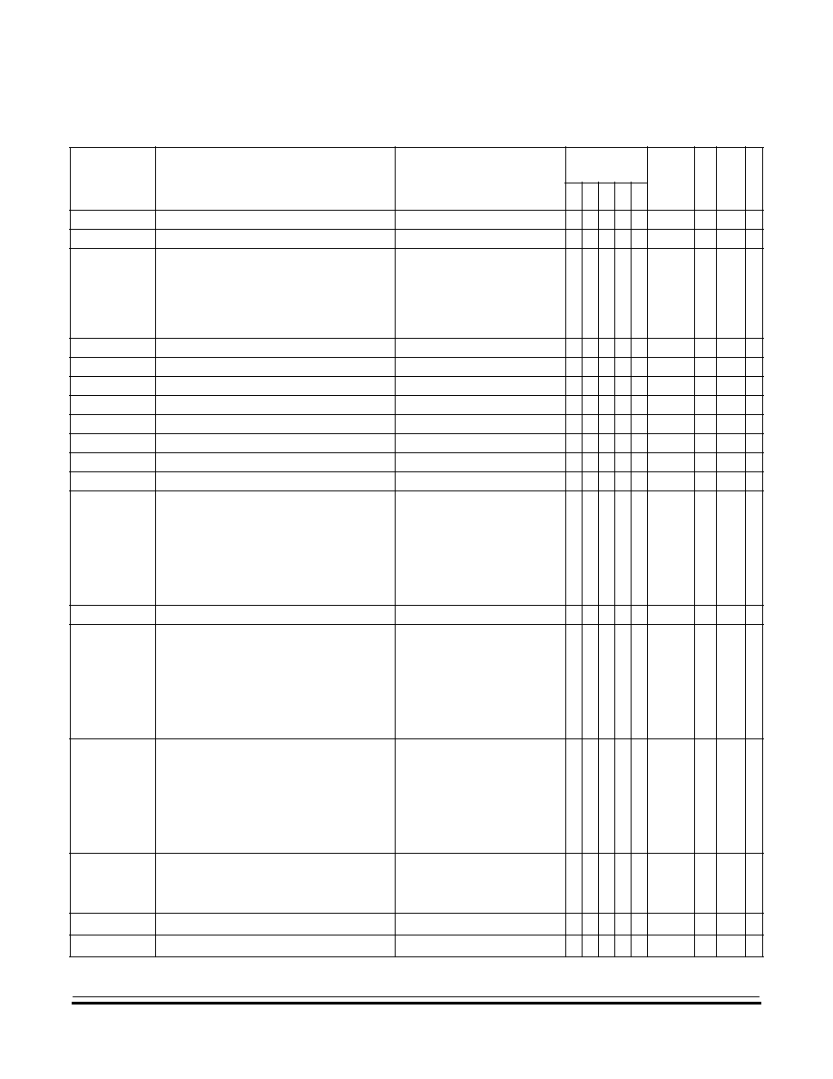
CPU and Instruction Set
Instruction Set Summary
MC68HC(7)05H12
--
Rev. 1.0
General Release Specification
MOTOROLA
CPU and Instruction Set
53
NON-DISCLOSURE AGREEMENT REQUIRED
BIH
rel
Branch if IRQ Pin High
PC
(PC) + 2 +
rel ? IRQ = 1
-- -- -- -- --
REL
2F
rr
3
BIL
rel
Branch if IRQ Pin Low
PC
(PC) + 2 +
rel ? IRQ = 0
-- -- -- -- --
REL
2E
rr
3
BIT #
opr
BIT
opr
BIT
opr
BIT
opr,X
BIT
opr,X
BIT ,X
Bit Test Accumulator with Memory Byte
(A)
(M)
-- --
§
§
--
IMM
DIR
EXT
IX2
IX1
IX
A5
B5
C5
D5
E5
F5
ii
dd
hh ll
ee ff
ff
2
3
4
5
4
3
BLO
rel
Branch if Lower (Same as BCS)
PC
(PC) + 2 +
rel ? C = 1
-- -- -- -- --
REL
25
rr
3
BLS
rel
Branch if Lower or Same
PC
(PC) + 2 +
rel ? C
Z = 1
-- -- -- -- --
REL
23
rr
3
BMC
rel
Branch if Interrupt Mask Clear
PC
(PC) + 2 +
rel ? I = 0
-- -- -- -- --
REL
2C
rr
3
BMI
rel
Branch if Minus
PC
(PC) + 2 +
rel ? N = 1
-- -- -- -- --
REL
2B
rr
3
BMS
rel
Branch if Interrupt Mask Set
PC
(PC) + 2 +
rel ? I = 1
-- -- -- -- --
REL
2D
rr
3
BNE
rel
Branch if Not Equal
PC
(PC) + 2 +
rel ? Z = 0
-- -- -- -- --
REL
26
rr
3
BPL
rel
Branch if Plus
PC
(PC) + 2 +
rel ? N = 0
-- -- -- -- --
REL
2A
rr
3
BRA
rel
Branch Always
PC
(PC) + 2 +
rel ? 1 = 1
-- -- -- -- --
REL
20
rr
3
BRCLR
n opr rel Branch if Bit n Clear
PC
(PC) + 2 +
rel ? Mn = 0
-- -- -- --
§
DIR (b0)
DIR (b1)
DIR (b2)
DIR (b3)
DIR (b4)
DIR (b5)
DIR (b6)
DIR (b7)
01
03
05
07
09
0B
0D
0F
dd rr
dd rr
dd rr
dd rr
dd rr
dd rr
dd rr
dd rr
5
5
5
5
5
5
5
5
BRN
rel
Branch Never
PC
(PC) + 2 +
rel ? 1 = 0
-- -- -- -- --
REL
21
rr
3
BRSET
n opr rel Branch if Bit n Set
PC
(PC) + 2 +
rel ? Mn = 1
-- -- -- --
§
DIR (b0)
DIR (b1)
DIR (b2)
DIR (b3)
DIR (b4)
DIR (b5)
DIR (b6)
DIR (b7)
00
02
04
06
08
0A
0C
0E
dd rr
dd rr
dd rr
dd rr
dd rr
dd rr
dd rr
dd rr
5
5
5
5
5
5
5
5
BSET
n opr
Set Bit n
Mn
1
-- -- -- -- --
DIR (b0)
DIR (b1)
DIR (b2)
DIR (b3)
DIR (b4)
DIR (b5)
DIR (b6)
DIR (b7)
10
12
14
16
18
1A
1C
1E
dd
dd
dd
dd
dd
dd
dd
dd
5
5
5
5
5
5
5
5
BSR
rel
Branch to Subroutine
PC
(PC) + 2; push (PCL)
SP
(SP) ≠ 1; push (PCH)
SP
(SP) ≠ 1
PC
(PC) +
rel
-- -- -- -- --
REL
AD
rr
6
CLC
Clear Carry Bit
C
0
-- -- -- -- 0
INH
98
2
CLI
Clear Interrupt Mask
I
0
-- 0 -- -- --
INH
9A
2
Table 3-6. Instruction Set Summary (Continued)
Source
Form
Operation
Description
Effect on
CCR
Address
Mode
Opcode
Operand
Cycles
H I N Z C

NON-DISCLOSURE AGREEMENT REQUIRED
CPU and Instruction Set
General Release Specification
MC68HC(7)05H12
--
Rev. 1.0
54
CPU and Instruction Set
MOTOROLA
CLR
opr
CLRA
CLRX
CLR
opr,X
CLR ,X
Clear Byte
M
$00
A
$00
X
$00
M
$00
M
$00
-- -- 0
1 --
DIR
INH
INH
IX1
IX
3F
4F
5F
6F
7F
dd
ff
5
3
3
6
5
CMP #
opr
CMP
opr
CMP
opr
CMP
opr,X
CMP
opr,X
CMP ,X
Compare Accumulator with Memory Byte
(A) ≠ (M)
-- --
§
§
§
IMM
DIR
EXT
IX2
IX1
IX
A1
B1
C1
D1
E1
F1
ii
dd
hh ll
ee ff
ff
2
3
4
5
4
3
COM
opr
COMA
COMX
COM
opr,X
COM ,X
Complement Byte (One's Complement)
M
(M) = $FF ≠ (M)
A
(A) = $FF ≠ (A)
X
(X) = $FF ≠ (X)
M
(M) = $FF ≠ (M)
M
(M) = $FF ≠ (M)
-- --
§
§
1
DIR
INH
INH
IX1
IX
33
43
53
63
73
dd
ff
5
3
3
6
5
CPX #
opr
CPX
opr
CPX
opr
CPX
opr,X
CPX
opr,X
CPX ,X
Compare Index Register with Memory Byte
(X) ≠ (M)
-- --
§
§
§
IMM
DIR
EXT
IX2
IX1
IX
A3
B3
C3
D3
E3
F3
ii
dd
hh ll
ee ff
ff
2
3
4
5
4
3
DEC
opr
DECA
DECX
DEC
opr,X
DEC ,X
Decrement Byte
M
(M) ≠ 1
A
(A) ≠ 1
X
(X) ≠ 1
M
(M) ≠ 1
M
(M) ≠ 1
-- --
§
§
--
DIR
INH
INH
IX1
IX
3A
4A
5A
6A
7A
dd
ff
5
3
3
6
5
EOR #
opr
EOR
opr
EOR
opr
EOR
opr,X
EOR
opr,X
EOR ,X
EXCLUSIVE OR Accumulator with Memory Byte
A
(A)
(M)
-- --
§
§
--
IMM
DIR
EXT
IX2
IX1
IX
A8
B8
C8
D8
E8
F8
ii
dd
hh ll
ee ff
ff
2
3
4
5
4
3
INC
opr
INCA
INCX
INC
opr,X
INC ,X
Increment Byte
M
(M) + 1
A
(A) + 1
X
(X) + 1
M
(M) + 1
M
(M) + 1
-- --
§
§
--
DIR
INH
INH
IX1
IX
3C
4C
5C
6C
7C
dd
ff
5
3
3
6
5
JMP
opr
JMP
opr
JMP
opr,X
JMP
opr,X
JMP ,X
Unconditional Jump
PC
Jump Address
-- -- -- -- --
DIR
EXT
IX2
IX1
IX
BC
CC
DC
EC
FC
dd
hh ll
ee ff
ff
2
3
4
3
2
Table 3-6. Instruction Set Summary (Continued)
Source
Form
Operation
Description
Effect on
CCR
Address
Mode
Opcode
Operand
Cycles
H I N Z C

CPU and Instruction Set
Instruction Set Summary
MC68HC(7)05H12
--
Rev. 1.0
General Release Specification
MOTOROLA
CPU and Instruction Set
55
NON-DISCLOSURE AGREEMENT REQUIRED
JSR
opr
JSR
opr
JSR
opr,X
JSR
opr,X
JSR ,X
Jump to Subroutine
PC
(PC) + n (n = 1, 2, or 3)
Push (PCL); SP
(SP) ≠ 1
Push (PCH); SP
(SP) ≠ 1
PC
Effective Address
-- -- -- -- --
DIR
EXT
IX2
IX1
IX
BD
CD
DD
ED
FD
dd
hh ll
ee ff
ff
5
6
7
6
5
LDA #
opr
LDA
opr
LDA
opr
LDA
opr,X
LDA
opr,X
LDA ,X
Load Accumulator with Memory Byte
A
(M)
-- --
§
§
--
IMM
DIR
EXT
IX2
IX1
IX
A6
B6
C6
D6
E6
F6
ii
dd
hh ll
ee ff
ff
2
3
4
5
4
3
LDX #
opr
LDX
opr
LDX
opr
LDX
opr,X
LDX
opr,X
LDX ,X
Load Index Register with Memory Byte
X
(M)
-- --
§
§
--
IMM
DIR
EXT
IX2
IX1
IX
AE
BE
CE
DE
EE
FE
ii
dd
hh ll
ee ff
ff
2
3
4
5
4
3
LSL
opr
LSLA
LSLX
LSL
opr,X
LSL ,X
Logical Shift Left (Same as ASL)
-- --
§
§
§
DIR
INH
INH
IX1
IX
38
48
58
68
78
dd
ff
5
3
3
6
5
LSR
opr
LSRA
LSRX
LSR
opr,X
LSR ,X
Logical Shift Right
-- -- 0
§
§
DIR
INH
INH
IX1
IX
34
44
54
64
74
dd
ff
5
3
3
6
5
MUL
Unsigned Multiply
X : A
(X)
◊
(A)
0 -- -- -- 0
INH
42
11
NEG
opr
NEGA
NEGX
NEG
opr,X
NEG ,X
Negate Byte (Two's Complement)
M
≠(M) = $00 ≠ (M)
A
≠(A) = $00 ≠ (A)
X
≠(X) = $00 ≠ (X)
M
≠(M) = $00 ≠ (M)
M
≠(M) = $00 ≠ (M)
-- --
§
§
§
DIR
INH
INH
IX1
IX
30
40
50
60
70
dd
ff
5
3
3
6
5
NOP
No Operation
-- -- -- -- --
INH
9D
2
ORA #
opr
ORA
opr
ORA
opr
ORA
opr,X
ORA
opr,X
ORA ,X
Logical OR Accumulator with Memory
A
(A)
(M)
-- --
§
§
--
IMM
DIR
EXT
IX2
IX1
IX
AA
BA
CA
DA
EA
FA
ii
dd
hh ll
ee ff
ff
2
3
4
5
4
3
ROL
opr
ROLA
ROLX
ROL
opr,X
ROL ,X
Rotate Byte Left through Carry Bit
-- --
§
§
§
DIR
INH
INH
IX1
IX
39
49
59
69
79
dd
ff
5
3
3
6
5
Table 3-6. Instruction Set Summary (Continued)
Source
Form
Operation
Description
Effect on
CCR
Address
Mode
Opcode
Operand
Cycles
H I N Z C
C
b0
b7
0
b0
b7
C
0
C
b0
b7

NON-DISCLOSURE AGREEMENT REQUIRED
CPU and Instruction Set
General Release Specification
MC68HC(7)05H12
--
Rev. 1.0
56
CPU and Instruction Set
MOTOROLA
ROR
opr
RORA
RORX
ROR
opr,X
ROR ,X
Rotate Byte Right through Carry Bit
-- --
§
§
§
DIR
INH
INH
IX1
IX
36
46
56
66
76
dd
ff
5
3
3
6
5
RSP
Reset Stack Pointer
SP
$00FF
-- -- -- -- --
INH
9C
2
RTI
Return from Interrupt
SP
(SP) + 1; Pull (CCR)
SP
(SP) + 1; Pull (A)
SP
(SP) + 1; Pull (X)
SP
(SP) + 1; Pull (PCH)
SP
(SP) + 1; Pull (PCL)
§
§
§
§
§
INH
80
9
RTS
Return from Subroutine
SP
(SP) + 1; Pull (PCH)
SP
(SP) + 1; Pull (PCL)
-- -- -- -- --
INH
81
6
SBC #
opr
SBC
opr
SBC
opr
SBC
opr,X
SBC
opr,X
SBC ,X
Subtract Memory Byte and Carry Bit from
Accumulator
A
(A) ≠ (M) ≠ (C)
-- --
§ §
§
IMM
DIR
EXT
IX2
IX1
IX
A2
B2
C2
D2
E2
F2
ii
dd
hh ll
ee ff
ff
2
3
4
5
4
3
SEC
Set Carry Bit
C
1
-- -- -- -- 1
INH
99
2
SEI
Set Interrupt Mask
I
1
-- 1 -- -- --
INH
9B
2
STA
opr
STA
opr
STA
opr,X
STA
opr,X
STA ,X
Store Accumulator in Memory
M
(A)
-- --
§
§
--
DIR
EXT
IX2
IX1
IX
B7
C7
D7
E7
F7
dd
hh ll
ee ff
ff
4
5
6
5
4
STX
opr
STX
opr
STX
opr,X
STX
opr,X
STX ,X
Store Index Register In Memory
M
(X)
-- --
§
§
--
DIR
EXT
IX2
IX1
IX
BF
CF
DF
EF
FF
dd
hh ll
ee ff
ff
4
5
6
5
4
SUB #
opr
SUB
opr
SUB
opr
SUB
opr,X
SUB
opr,X
SUB ,X
Subtract Memory Byte from Accumulator
A
(A) ≠ (M)
-- --
§
§
§
IMM
DIR
EXT
IX2
IX1
IX
A0
B0
C0
D0
E0
F0
ii
dd
hh ll
ee ff
ff
2
3
4
5
4
3
SWI
Software Interrupt
PC
(PC) + 1; Push (PCL)
SP
(SP) ≠ 1; Push (PCH)
SP
(SP) ≠ 1; Push (X)
SP
(SP) ≠ 1; Push (A)
SP
(SP) ≠ 1; Push (CCR)
SP
(SP) ≠ 1; I
1
PCH
Interrupt Vector High Byte
PCL
Interrupt Vector Low Byte
-- 1 -- -- --
INH
83
10
TAX
Transfer Accumulator to Index Register
X
(A)
-- -- -- -- --
INH
97
2
Table 3-6. Instruction Set Summary (Continued)
Source
Form
Operation
Description
Effect on
CCR
Address
Mode
Opcode
Operand
Cycles
H I N Z C
b0
b7
C
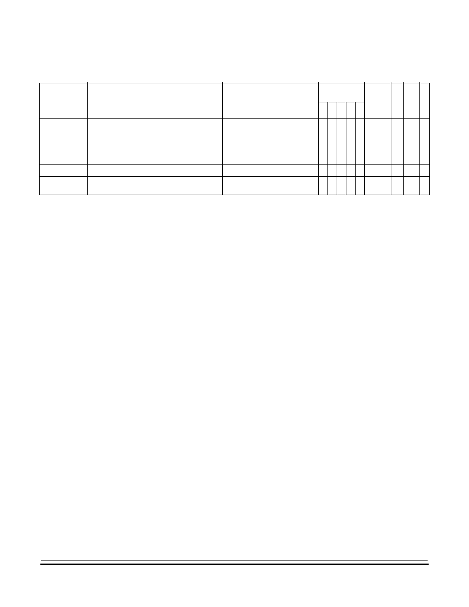
CPU and Instruction Set
Instruction Set Summary
MC68HC(7)05H12
--
Rev. 1.0
General Release Specification
MOTOROLA
CPU and Instruction Set
57
NON-DISCLOSURE AGREEMENT REQUIRED
TST
opr
TSTA
TSTX
TST
opr,X
TST ,X
Test Memory Byte for Negative or Zero
(M) ≠ $00
-- --
§
§
--
DIR
INH
INH
IX1
IX
3D
4D
5D
6D
7D
dd
ff
4
3
3
5
4
TXA
Transfer Index Register to Accumulator
A
(X)
-- -- -- -- --
INH
9F
2
WAIT
Stop CPU Clock and Enable Interrupts
--
0
-- -- --
INH
8F
2
A
Accumulator
opr
Operand (one or two bytes)
C
Carry/borrow flag
PC
Program counter
CCR
Condition code register
PCH Program counter high byte
dd
Direct address of operand
PCL Program counter low byte
dd rr
Direct address of operand and relative offset of branch instruction
REL Relative addressing mode
DIR
Direct addressing mode
rel
Relative program counter offset byte
ee ff
High and low bytes of offset in indexed, 16-bit offset addressing
rr
Relative program counter offset byte
EXT
Extended addressing mode
SP
Stack pointer
ff
Offset byte in indexed, 8-bit offset addressing
X
Index register
H
Half-carry flag
Z
Zero flag
hh ll
High and low bytes of operand address in extended addressing
#
Immediate value
I
Interrupt mask
Logical AND
ii
Immediate operand byte
Logical OR
IMM
Immediate addressing mode
Logical EXCLUSIVE OR
INH
Inherent addressing mode
( )
Contents of
IX
Indexed, no offset addressing mode
≠( )
Negation (two's complement)
IX1
Indexed, 8-bit offset addressing mode
Loaded with
IX2
Indexed, 16-bit offset addressing mode
?
If
M
Memory location
:
Concatenated with
N
Negative flag
§
Set or cleared
n
Any bit
--
Not affected
Table 3-6. Instruction Set Summary (Continued)
Source
Form
Operation
Description
Effect on
CCR
Address
Mode
Opcode
Operand
Cycles
H I N Z C

NON-DISCLOSURE AGREEMENT REQUIRED
CPU and Instruction Set
General Release Specification
MC68HC(7)05H12
--
Rev. 1.0
58
CPU and Instruction Set
MOTOROLA
T
a
b
le 3-7.
Opcode Map
Bit Manipulation
Branch
Read-Modify-Write
Control
Register/Memory
DIR
DIR
REL
DIR
INH
INH
IX1
IX
INH
INH
IMM
DIR
EXT
IX2
IX1
IX
0123456789
ABCD
E
F
0
5
BRSET0
3
DIR
5
BSET0
2
DIR
3
BRA
2
REL
5
NEG
2
DIR
3
NEGA
1
INH
3
NEGX
1
INH
6
NEG
2
IX1
5
NEG
1I
X
9
RT
I
1
INH
2
SUB
2
IMM
3
SUB
2
DIR
4
SUB
3
EXT
5
SUB
3
IX2
4
SUB
2
IX1
3
SUB
1I
X
0
1
5
BRCLR0
3
DIR
5
BCLR0
2
DIR
3
BRN
2
REL
6
RT
S
1
INH
2
CMP
2
IMM
3
CMP
2
DIR
4
CMP
3
EXT
5
CMP
3
IX2
4
CMP
2
IX1
3
CMP
1I
X
1
2
5
BRSET1
3
DIR
5
BSET1
2
DIR
3
BHI
2
REL
11
MUL
1
INH
2
SBC
2
IMM
3
SBC
2
DIR
4
SBC
3
EXT
5
SBC
3
IX2
4
SBC
2
IX1
3
SBC
1I
X
2
3
5
BRCLR1
3
DIR
5
BCLR1
2
DIR
3
BLS
2
REL
5
COM
2
DIR
3
COMA
1
INH
3
COMX
1
INH
6
COM
2
IX1
5
COM
1I
X
10
SWI
1
INH
2
CPX
2
IMM
3
CPX
2
DIR
4
CPX
3
EXT
5
CPX
3
IX2
4
CPX
2
IX1
3
CPX
1I
X
3
4
5
BRSET2
3
DIR
5
BSET2
2
DIR
3
BCC
2
REL
5
LSR
2
DIR
3
LSRA
1
INH
3
LSRX
1
INH
6
LSR
2
IX1
5
LSR
1I
X
2
AND
2
IMM
3
AND
2
DIR
4
AND
3
EXT
5
AND
3
IX2
4
AND
2
IX1
3
AND
1I
X
4
5
5
BRCLR2
3
DIR
5
BCLR2
2
DIR
3
BCS/BLO
2
REL
2
BIT
2
IMM
3
BIT
2
DIR
4
BIT
3
EXT
5
BIT
3
IX2
4
BIT
2
IX1
3
BIT
1I
X
5
6
5
BRSET3
3
DIR
5
BSET3
2
DIR
3
BNE
2
REL
5
RO
R
2
DIR
3
R
ORA
1
INH
3
R
ORX
1
INH
6
RO
R
2
IX1
5
RO
R
1I
X
2
LD
A
2
IMM
3
LD
A
2
DIR
4
LD
A
3
EXT
5
LD
A
3
IX2
4
LD
A
2
IX1
3
LD
A
1I
X
6
7
5
BRCLR3
3
DIR
5
BCLR3
2
DIR
3
BEQ
2
REL
5
ASR
2
DIR
3
ASRA
1
INH
3
ASRX
1
INH
6
ASR
2
IX1
5
ASR
1I
X
2
TA
X
1
INH
4
ST
A
2
DIR
5
ST
A
3
EXT
6
ST
A
3
IX2
5
ST
A
2
IX1
4
ST
A
1I
X
7
8
5
BRSET4
3
DIR
5
BSET4
2
DIR
3
BHCC
2
REL
5
ASL/LSL
2
DIR
3
ASLA/LSLA
1
INH
3
ASLX/LSLX
1
INH
6
ASL/LSL
2
IX1
5
ASL/LSL
1I
X
2
CLC
1
INH
2
EOR
2
IMM
3
EOR
2
DIR
4
EOR
3
EXT
5
EOR
3
IX2
4
EOR
2
IX1
3
EOR
1I
X
8
9
5
BRCLR4
3
DIR
5
BCLR4
2
DIR
3
BHCS
2
REL
5
RO
L
2
DIR
3
R
OLA
1
INH
3
R
OLX
1
INH
6
RO
L
2
IX1
5
RO
L
1I
X
2
SEC
1
INH
2
ADC
2
IMM
3
ADC
2
DIR
4
ADC
3
EXT
5
ADC
3
IX2
4
ADC
2
IX1
3
ADC
1I
X
9
A
5
BRSET5
3
DIR
5
BSET5
2
DIR
3
BPL
2
REL
5
DEC
2
DIR
3
DECA
1
INH
3
DECX
1
INH
6
DEC
2
IX1
5
DEC
1I
X
2
CLI
1
INH
2
ORA
2
IMM
3
ORA
2
DIR
4
ORA
3
EXT
5
ORA
3
IX2
4
ORA
2
IX1
3
ORA
1I
X
A
B
5
BRCLR5
3
DIR
5
BCLR5
2
DIR
3
BMI
2
REL
2
SEI
1
INH
2
ADD
2
IMM
3
ADD
2
DIR
4
ADD
3
EXT
5
ADD
3
IX2
4
ADD
2
IX1
3
ADD
1I
X
B
C
5
BRSET6
3
DIR
5
BSET6
2
DIR
3
BMC
2
REL
5
INC
2
DIR
3
INCA
1
INH
3
INCX
1
INH
6
INC
2
IX1
5
INC
1I
X
2
RSP
1
INH
2
JMP
2
DIR
3
JMP
3
EXT
4
JMP
3
IX2
3
JMP
2
IX1
2
JMP
1I
X
C
D
5
BRCLR6
3
DIR
5
BCLR6
2
DIR
3
BMS
2
REL
4
TST
2
DIR
3
TST
A
1
INH
3
TSTX
1
INH
5
TST
2
IX1
4
TST
1I
X
2
NOP
1
INH
6
BSR
2
REL
5
JSR
2
DIR
6
JSR
3
EXT
7
JSR
3
IX2
6
JSR
2
IX1
5
JSR
1I
X
D
E
5
BRSET7
3
DIR
5
BSET7
2
DIR
3
BIL
2
REL
2
LDX
2
IMM
3
LDX
2
DIR
4
LDX
3
EXT
5
LDX
3
IX2
4
LDX
2
IX1
3
LDX
1I
X
E
F
5
BRCLR7
3
DIR
5
BCLR7
2
DIR
3
BIH
2
REL
5
CLR
2
DIR
3
CLRA
1
INH
3
CLRX
1
INH
6
CLR
2
IX1
5
CLR
1I
X
2
W
AIT
1
INH
2
TXA
1
INH
4
STX
2
DIR
5
STX
3
EXT
6
STX
3
IX2
5
STX
2
IX1
4
STX
1I
X
F
INH = InherentREL = Relativ
e
IMM = ImmediateIX = Inde
x
ed, No Offset
DIR = DirectIX1 = Inde
x
ed, 8-Bit Offset
EXT = ExtendedIX2 = Inde
x
ed, 16-Bit Offset
0
MSB of Opcode in Hexadecimal
LSB of Opcode in Hexadecimal
0
5
BRSET0
3
DIR
Number of Cycles
Opcode Mnemonic
Number of Bytes/Addressing Mode
LSB
MSB
LSB
MSB
LSB
MSB

MC68HC(7)05H12
--
Rev. 1.0
General Release Specification
MOTOROLA
Interrupts
59
NON-DISCLOSURE AGREEMENT REQUIRED
General Release Specification -- MC68HC(7)05H12
Section 4. Interrupts
4.1 Contents
4.2
Introduction . . . . . . . . . . . . . . . . . . . . . . . . . . . . . . . . . . . . . . . . 60
4.3
CPU Interrupt Processing . . . . . . . . . . . . . . . . . . . . . . . . . . . . . 60
4.4
Reset Interrupt Sequence. . . . . . . . . . . . . . . . . . . . . . . . . . . . . 63
4.5
Software Interrupt (SWI) . . . . . . . . . . . . . . . . . . . . . . . . . . . . . . 63
4.6
Hardware Interrupts . . . . . . . . . . . . . . . . . . . . . . . . . . . . . . . . . 63
4.7
External Interrupt (IRQ/Keyboard) . . . . . . . . . . . . . . . . . . . . . . 63
4.8
8-Bit Timer Interrupt . . . . . . . . . . . . . . . . . . . . . . . . . . . . . . . . . 64
4.9
16-Bit Timer1 Interrupt . . . . . . . . . . . . . . . . . . . . . . . . . . . . . . . 64
4.10
16-Bit Timer2 Interrupt . . . . . . . . . . . . . . . . . . . . . . . . . . . . . . . 64
4.11
SCI Interrupt . . . . . . . . . . . . . . . . . . . . . . . . . . . . . . . . . . . . . . . 65
4.12
SPI Interrupt . . . . . . . . . . . . . . . . . . . . . . . . . . . . . . . . . . . . . . . 65
4.13
WAIT Mode. . . . . . . . . . . . . . . . . . . . . . . . . . . . . . . . . . . . . . . . 65

NON-DISCLOSURE AGREEMENT REQUIRED
Interrupts
General Release Specification
MC68HC(7)05H12
--
Rev. 1.0
60
Interrupts
MOTOROLA
4.2 Introduction
The MCU can be interrupted eight different ways:
1. Nonmaskable Software Interrupt Instruction (SWI)
2. External Asynchronous Interrupt (IRQ)
3. External Keyboard Wakeup on Port A
4. Internal 8 bit Timer Interrupt (CTIMER)
5. Internal 16-bit Timer1 Interrupt (TIMER1)
6. Internal 16-bit Timer2 Interrupt (TIMER2)
7. Internal Serial Communications Interface Interrupt (SCI)
8. Internal Serial Peripheral Interface Interrupt (SPI)
4.3 CPU Interrupt Processing
Interrupts cause the processor to save register contents on the stack
and to set the interrupt mask (I-bit) to prevent additional interrupts.
Unlike RESET, hardware interrupts do not cause the current instruction
execution to be halted, but are considered pending until the current
instruction is complete.
If interrupts are not masked (I-bit in the CCR is clear) and the
corresponding interrupt enable bit is set, then the processor will proceed
with interrupt processing. Otherwise, the next instruction is fetched and
executed. If an interrupt occurs the processor completes the current
instruction, then stacks the current CPU register states, sets the I-bit to
inhibit further interrupts, and finally checks the pending hardware
interrupts. If more than one interrupt is pending following the stacking
operation, the interrupt with the highest vector location shown in
Table 4-1 will be serviced first. The SWI is executed the same as any
other instruction, regardless of the I-bit state.
When an interrupt is to be processed the CPU fetches the address of the
appropriate interrupt software service routine from the vector table at
locations $3FF0 to $3FFF as defined in Table 4-1.

Interrupts
CPU Interrupt Processing
MC68HC(7)05H12
--
Rev. 1.0
General Release Specification
MOTOROLA
Interrupts
61
NON-DISCLOSURE AGREEMENT REQUIRED
The M68HC05 CPU does not support interruptible instructions,
therefore, the maximum latency to the first instruction of the interrupt
service routine must include the longest instruction execution time plus
stacking overhead.
Latency = (Longest instruction execution time + 10) x t
CYC
secs
An RTI instruction is used to signify when the interrupt software service
routine is completed. The RTI instruction causes the register contents to
be recovered from the stack and normal processing to resume at the
next instruction that was to be executed when the interrupt took place.
Figure 4-1 shows the sequence of events that occur during interrupt
processing.
Table 4-1. Reset/Interrupt Vector Addresses
Function
Source
Local
Mask
Global
Mask
Priority
(1 = Highest)
Vector
Address
Reset
Power-On Logic
None
None
1
$3FFE≠$3FFF
RESET Pin
COP Watchdog
Software
Interrupt
(SWI)
User Code
None
None
Same Priority
As Instruction
$3FFC≠$3FFD
External
Interrupt /
IRQ Pin
None
I Bit
2
$3FFA≠$3FFB
KEY wakeup
PTA KEY Pins
PAIE Bits
Core Timer
Interrupts
RTIF Bit
RTIE Bit
I Bit
3
$3FF8≠$3FF9
TOF Bit
TOFE Bit
16-Bit Timer 1
Interrupts
ICF Bits
ICIE Bits
I Bit
4
$3FF6≠$3FF7
OCF Bits
OCIE Bits
TOF Bit
TOIE Bit
16-Bit Timer 2
Interrupts
ICF Bits
ICIE Bits
I Bit
5
$3FF4≠$3FF5
OCF Bits
OCIE Bits
TOF Bit
TOIE Bit
SPI
Interrupts
SPIF Bit
SPIE
I Bit
6
$3FF2≠$3FF3
MODF Bit
SCI
Interrupts
TDRE Bit
TCIE Bit
I Bit
7
$3FF0≠$3FF1
TC Bit
RDRF Bit
RIE Bit
OR Bit
IDLE Bit
ILIE Bit

NON-DISCLOSURE AGREEMENT REQUIRED
Interrupts
General Release Specification
MC68HC(7)05H12
--
Rev. 1.0
62
Interrupts
MOTOROLA
Figure 4-1. Interrupt Processing Flowchart
Y
Y
Y
Y
Y
Y
Y
Y
FROM
RESET
I-BIT
IN CCR
SET?
IRQ/KEY
EXTERNAL
INTERRUPT
CLEAR IRQ
REQUEST
LATCH
INTERNAL
8 BIT CORE TIMER
INTERRUPT
INTERNAL
16 BIT TIMER1
INTERRUPT
INTERNAL
16 BIT TIMER2
INTERRUPT
INTERNAL
SPI
INTERRUPT
INTERNAL
SCI
INTERRUPT
SWI
INSTRUCTION
?
RTI
INSTRUCTION
?
EXECUTE
INSTRUCTION
RESTORE REGISTERS
FROM STACK:
CCR,A,X,PC
SET I BIT IN
CC REGISTER
LOAD PC FROM
APPROPRIATE
VECTOR
FETCH NEXT INSTRUCTION
Y
STACK
PC,X,A,CCR
N
N
N
N
N
N
N
N
N

Interrupts
Reset Interrupt Sequence
MC68HC(7)05H12
--
Rev. 1.0
General Release Specification
MOTOROLA
Interrupts
63
NON-DISCLOSURE AGREEMENT REQUIRED
4.4 Reset Interrupt Sequence
The reset function is not in the strictest sense an interrupt; however, it is
acted upon in a similar manner as shown in Figure 4-1. A low level input
on the RESET pin or internally generated RST signal causes the
program to vector to its starting address which is specified by the
contents of memory locations $3FFE and $3FFF. The I-bit in the
condition code register is also set. The MCU is configured to a known
state during this type of reset as described in Section 5 Resets.
4.5 Software Interrupt (SWI)
The SWI is an executable instruction and a non-maskable interrupt since
it is executed regardless of the state of the I-bit in the CCR. If the I-bit is
zero (interrupts enabled), the SWI instruction executes after interrupts
which were pending before the SWI was fetched, or before interrupts
generated after the SWI was fetched. The interrupt service routine
address is specified by the contents of memory locations $3FFC and
$3FFD.
4.6 Hardware Interrupts
All hardware interrupts except reset are maskable by the I-bit in the
CCR. If the I-bit is set, all hardware interrupts (internal and external) are
disabled. Clearing the I-bit enables the hardware interrupts. There are
two types of hardware interrupts (external, internal) which are explained
in the following sections.
4.7 External Interrupt (IRQ/Keyboard)
If the interrupt mask bit (I bit) of the CCR is set, all maskable interrupts
(internal and external) are disabled. Clearing the I bit enables interrupts.
The interrupt request is latched immediately following the falling edge of
IRQ. It is then synchronized internally and serviced by the interrupt
service routine located at the address specified by the contents of
$3FFA and $3FFB.

NON-DISCLOSURE AGREEMENT REQUIRED
Interrupts
General Release Specification
MC68HC(7)05H12
--
Rev. 1.0
64
Interrupts
MOTOROLA
Either a level-sensitive and edge-sensitive trigger, or an edge-sensitive-
only trigger can be implemented by software.
NOTE:
The internal interrupt latch is cleared in the first part of the interrupt
service routine; therefore, one external interrupt pulse could be latched
and serviced as soon as the I bit is cleared.
The BIH and BIL instructions will only apply to the level on the IRQ pin
itself, and not to the output of the logic OR function with the Port A
keyboard wakeup interrupts. The state of the individual Port A pins can
be checked by reading the appropriate Port A pins as inputs.
4.8 8-Bit Timer Interrupt
This timer can create two types of interrupts. A timer overflow interrupt
will occur whenever the 8-bit timer rolls over from $FF to $00 and the
enable bit TOFE is set. A real time interrupt will occur whenever the
programmed time elapses and the enable bit RTIE is set. This interrupt
will vector to the interrupt service routine located at the address specified
by the contents of memory location $3FF8 and $3FF9.
4.9 16-Bit Timer1 Interrupt
There are five different timer interrupt flags that cause a 16-bit timer1
interrupt whenever they are set and enabled. The interrupt flags are in
the timer1 status register (TSR), and the enable bits are in the timer1
control register1 (TCR1). Any of these interrupts will vector to the same
interrupt service routine, located at the address specified by the contents
of memory location $3FF6 and $3FF7.
4.10 16-Bit Timer2 Interrupt
There are five different timer interrupt flags that cause a 16-bit timer2
interrupt whenever they are set and enabled. The interrupt flags are in
the timer2 status register (TSR), and the enable bits are in the timer2
control register1 (TCR1). Any of these interrupts will vector to the same

Interrupts
SCI Interrupt
MC68HC(7)05H12
--
Rev. 1.0
General Release Specification
MOTOROLA
Interrupts
65
NON-DISCLOSURE AGREEMENT REQUIRED
interrupt service routine, located at the address specified by the contents
of memory location $3FF4 and $3FF5.
4.11 SCI Interrupt
There are five different interrupt flags (TDRE, TC, OR, RDRF, IDLE) that
will cause an SCI interrupt whenever they are set and enabled. These
five interrupt flags are found in the five most significant bits of the SCI
status register SCSR. The actual processor interrupt is generated only if
the I-bit in the condition code register is clear and the enable bit in the
serial communications control register 2 (SCCR2) is enabled. The SCI
interrupt causes the program counter to vector to the address pointed to
by memory locations $3FF2≠$3FF3 which contain the start address of
the interrupt service routine. Software in the SCI interrupt service routine
must determine the priority and cause of the SCI interrupt by examining
the interrupt flags and the status bits in the serial communications status
register (SCSR).
4.12 SPI Interrupt
There are two different SPI interrupt flags that cause an SPI interrupt
whenever they are set and enabled. The interrupt flags are in the SPI
status register (SPSR), and the enable bits are in the SPI control register
(SPCR). Either of these interrupts will vector to the same interrupt
service routine, located at the address specified by the contents of
memory locations $3FF0 and $3FF1.
4.13 WAIT Mode
All modules that are capable of generating interrupts in WAIT mode will
be allowed to do so if the module is configured properly. The I-bit is
automatically cleared when WAIT mode is entered. Interrupts detected
on port A are recognized in WAIT modes.

NON-DISCLOSURE AGREEMENT REQUIRED
Interrupts
General Release Specification
MC68HC(7)05H12
--
Rev. 1.0
66
Interrupts
MOTOROLA

MC68HC(7)05H12
--
Rev. 1.0
General Release Specification
MOTOROLA
Resets
67
NON-DISCLOSURE AGREEMENT REQUIRED
General Release Specification -- MC68HC(7)05H12
Section 5. Resets
5.1 Contents
5.2
Introduction . . . . . . . . . . . . . . . . . . . . . . . . . . . . . . . . . . . . . . . . 67
5.3
External Reset (RESET). . . . . . . . . . . . . . . . . . . . . . . . . . . . . . 67
5.4
Internal Resets . . . . . . . . . . . . . . . . . . . . . . . . . . . . . . . . . . . . . 68
5.5
Power-On Reset (POR) . . . . . . . . . . . . . . . . . . . . . . . . . . . . . . 70
5.6
Computer Operating Properly Reset (COPR). . . . . . . . . . . . . . 70
5.6.1
Resetting the COP . . . . . . . . . . . . . . . . . . . . . . . . . . . . . . . 70
5.6.2
COP During WAIT Mode . . . . . . . . . . . . . . . . . . . . . . . . . . . 71
5.6.3
COP Watchdog Timer Considerations . . . . . . . . . . . . . . . . 71
5.6.4
COP Register . . . . . . . . . . . . . . . . . . . . . . . . . . . . . . . . . . . 72
5.7
Illegal Address Reset . . . . . . . . . . . . . . . . . . . . . . . . . . . . . . . . 72
5.8
Low Voltage Reset (LVR) . . . . . . . . . . . . . . . . . . . . . . . . . . . . . 72
5.8.1
LVR Operation in WAIT. . . . . . . . . . . . . . . . . . . . . . . . . . . . 73
5.2 Introduction
The MCU can be reset from five sources: one external input and four
internal restart conditions. The RESET pin is an input with a Schmitt
trigger. All the internal peripheral modules will be reset by the internal
reset signal (RST). Refer to Figure 5-2 for reset timing detail. The
RESET pin contains an internal pullup device.
5.3 External Reset (RESET)
The RESET pin is the only external source of a reset. This pin is
connected to a Schmitt trigger input gate to provide an upper and lower
threshold voltage separated by a minimum amount of hysteresis. This
external reset occurs whenever the RESET pin is pulled below the lower

NON-DISCLOSURE AGREEMENT REQUIRED
Resets
General Release Specification
MC68HC(7)05H12
--
Rev. 1.0
68
Resets
MOTOROLA
threshold and remains in reset until the RESET pin rises above the
upper threshold. This active low input will generate the RST signal and
reset the CPU and peripherals. When the RESET pin goes high, the
MCU will resume operation on the following cycle.
NOTE:
Activation of the RST signal is generally referred to as reset of the
device, unless otherwise specified.
The RESET pin can also act as an open drain output. It will be pulled to
a low state by an internal pulldown that is activated by any reset source.
This RESET pulldown device will be asserted for 3≠4 cycles of the
internal clock, f
OP
, or as long as an internal reset source is asserted.
When the external RESET pin is asserted, the pulldown device will be
turned on for the 3≠4 internal clock cycles.
5.4 Internal Resets
The four internally generated resets are the initial power-on reset
function, the COP Watchdog Timer reset, the illegal address detector,
and the low voltage reset. All internal resets will also assert (pull to logic
zero) the external RESET pin for the duration of the reset or 3≠4 internal
clock cycles, whichever is longer.
Figure 5-1. Internal Resets
INTERNAL
RESETS
RESET
PIN
VDD
INTERNAL
RESET
LOGIC
INTERNAL
PULLUP

MC68HC(7)05H12
--
Rev. 1.0
General Release Specification
MOTOROLA
Resets
69
Resets
Internal Resets
NON-DISCLOSURE AGREEMENT REQUIRED
Figure 5-2. RESET
and POR Timing Diagram
PCH
PCL
OSC1
2
RESET
INTERNAL
ADDRESS
BUS
1
3FFE
3FFF
V
DD
4064 t
cyc
t cyc
t RL
INTERNAL
DATA
BUS
1
3FFE
3FFE
3FFE
3FFE
NEW PC
3FFF
NOTES:
1.
Internal timing signal and bus information not available externally.
2.
OSC1 line is not meant to represent frequency. It is only used to represent time.
3.
The next rising edge of the internal processor clock following the rising edge of RESET
initiates the reset sequence.
4.
V
DD
must fall to a level lower than V
POR
in order to recognized as a power on reset.
If LVR is enabled, VDD must fall below the LVR Power Off Reset Voltage VROFF.
3
NEW
NEW
OP
CODE
PCL
PCH
NEW PC
NEW PC
OP
CODE
NEW PC
0v
POR THRESHOLD (TYP. 1-2V) 4
INTERNAL
PROCESSOR
CLOCK
1

NON-DISCLOSURE AGREEMENT REQUIRED
Resets
General Release Specification
MC68HC(7)05H12
--
Rev. 1.0
70
Resets
MOTOROLA
5.5 Power-On Reset (POR)
The internal POR is generated on power-up to allow the clock oscillator
to stabilize. The POR is strictly for power turn-on conditions and is not
able to detect a drop in the power supply voltage (brown-out). There is
an oscillator stabilization delay of 4064 internal processor bus clock
cycles after the oscillator becomes active.
The POR will generate the RST signal which will reset the CPU. If any
other reset function is active at the end of this 4064 cycle delay, the RST
signal will remain in the reset condition until the other reset condition(s)
end.
POR will activate the RESET pin pulldown device connected to the pin.
V
DD
must drop below V
POR
in order for the internal POR circuit to detect
the next rise of V
DD
.
5.6 Computer Operating Properly Reset (COPR)
The MCU contains a watchdog timer that automatically times out if not
reset (cleared) within a specific time by a program reset sequence. If the
COP watchdog timer is allowed to time-out, an internal reset is
generated to reset the MCU. Regardless of an internal or external reset,
the MCU comes out of a COP reset according to the pin conditions that
determine mode selection.
The COP reset function is enabled or disabled by the Mask option (COP)
and is verified during production testing.
The COP Watchdog reset will activate the internal pulldown device
connected to the RESET pin.
5.6.1 Resetting the COP
Preventing a COP reset is done by writing a `0' to the COPR bit. This
action will reset the counter and begin the time-out period again. The
COPR bit is bit 0 of address $3FF0. A read of address $3FF0 will return
user data programmed at that location.

Resets
Computer Operating Properly Reset (COPR)
MC68HC(7)05H12
--
Rev. 1.0
General Release Specification
MOTOROLA
Resets
71
NON-DISCLOSURE AGREEMENT REQUIRED
5.6.2 COP During WAIT Mode
The COP will continue to operate normally during WAIT mode. The
system should be configured to pull the device out of WAIT mode
periodically and reset the COP by writing to the COPR bit to prevent a
COP reset.
5.6.3 COP Watchdog Timer Considerations
The COP Watchdog Timer is active in User Mode if enabled by the Mask
option (COP).
If the COP Watchdog Timer is selected, the COP will reset the MCU
when it times out. Therefore, it is recommended that the COP Watchdog
should be disabled for a system that must have intentional uses of the
WAIT Mode for periods longer than the COP time-out period.

NON-DISCLOSURE AGREEMENT REQUIRED
Resets
General Release Specification
MC68HC(7)05H12
--
Rev. 1.0
72
Resets
MOTOROLA
5.6.4 COP Register
The COP register is shared with the MSB of a user interrupt vector as
shown in Figure 5-3. Reading this location will return whatever user data
has been programmed at this location. Writing a `0' to the COPR bit in
this location will clear the COP watchdog timer.
5.7 Illegal Address Reset
An illegal address reset is generated when the CPU attempts to fetch an
instruction from either unimplemented address space ($0150 to $03FF,
$0500 to $0FFF), Monitor ROM ($3F00 to $3FEF) or I/O address space
($0000 to $004F).
The illegal address reset will activate the internal pulldown device
connected to the RESET pin.
NOTE:
No RTS, RTI or JMP,X instruction should be placed at the end of a
memory block (RAM $014F, EEPROM $04FF, User ROM $3EFF) since
this results in an illegal address reset.
5.8 Low Voltage Reset (LVR)
The internal low voltage (LVR) reset is generated when V
DD
falls below
the LVR threshold V
ROFF
and will be release following a POR delay
starting when V
DD
rises above V
RON
. The LVR threshold is tested to be
above the minimum operating voltage of the microcontroller and is
intended to assure that the CPU will be held in reset when the V
DD
supply voltage is below reasonable operating limits. A mask option is
$3FF0
Bit 7
6
5
4
3
2
1
Bit 0
Read:
Write:
COPR
Reset:
Figure 5-3. COP Watchdog Timer Location Register (COPR)
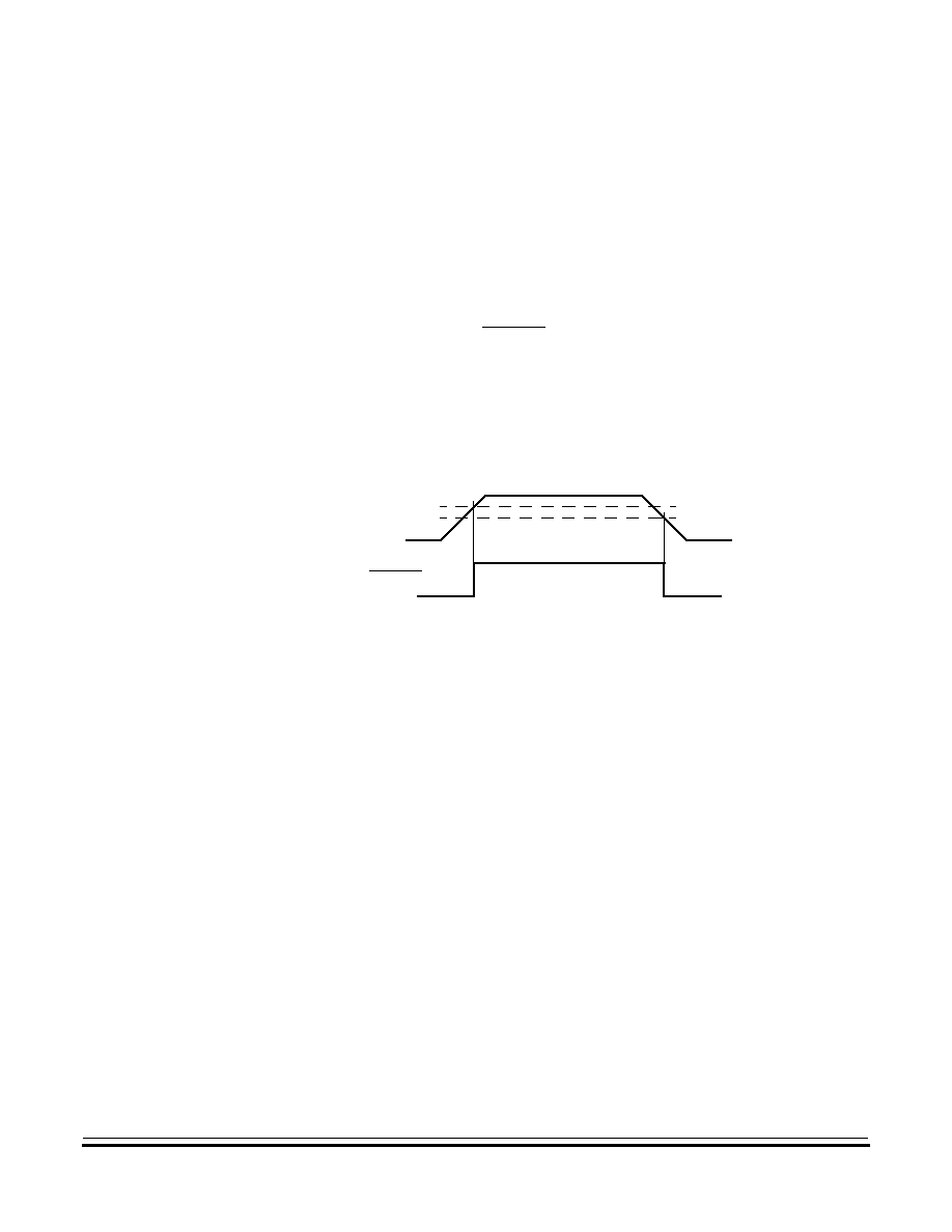
Resets
Low Voltage Reset (LVR)
MC68HC(7)05H12
--
Rev. 1.0
General Release Specification
MOTOROLA
Resets
73
NON-DISCLOSURE AGREEMENT REQUIRED
provided to disable the LVR when the device is expected to normally
operate at low voltages. Note that the V
DD
rise and fall slew rates must
be within the specification for proper LVR operation. If the specification
is not met, the circuit will operate properly following a delay of V
DD
/Slew
rate.
The LVR will generate the RST signal which will reset the CPU and other
peripherals. The low voltage reset will activate the internal pulldown
device connected to the RESET pin.
If any other reset function is active at the end of the LVR reset signal, the
RST signal will remain in the reset condition until the other reset
condition(s) end.
Figure 5-4. Low Voltage Reset
NOTE:
An external capacity at the RST pin increases the reaction time for the
generation of the internal reset and allows V
DD
drops. Refer to Figure 5-1.
5.8.1 LVR Operation in WAIT
If enabled, the LVR supply voltage sense option is active during WAIT.
Any reset source can bring the MCU out of WAIT mode.
VRON
VROFF
VDD
RESET
HYSTERESIS

NON-DISCLOSURE AGREEMENT REQUIRED
Resets
General Release Specification
MC68HC(7)05H12
--
Rev. 1.0
74
Resets
MOTOROLA

Operating Modes
Contents
MC68HC(7)05H12
--
Rev. 1.0
General Release Specification
MOTOROLA
Operating Modes
75
NON-DISCLOSURE AGREEMENT REQUIRED
6.1 Contents
6.2
Introduction . . . . . . . . . . . . . . . . . . . . . . . . . . . . . . . . . . . . . . . . 75
6.3
User Mode . . . . . . . . . . . . . . . . . . . . . . . . . . . . . . . . . . . . . . . . 75
6.4
Monitor Mode . . . . . . . . . . . . . . . . . . . . . . . . . . . . . . . . . . . . . . 76
6.5
Low Power Modes . . . . . . . . . . . . . . . . . . . . . . . . . . . . . . . . . . 76
6.5.1
WAIT Mode . . . . . . . . . . . . . . . . . . . . . . . . . . . . . . . . . . . . . 77
6.5.2
Data Retention Mode . . . . . . . . . . . . . . . . . . . . . . . . . . . . . 78
6.5.3
Slow Mode. . . . . . . . . . . . . . . . . . . . . . . . . . . . . . . . . . . . . . 78
6.2 Introduction
The normal operating mode of the MC68HC(7)05H12 is user (or single
chip) mode. There is also a monitor (or bootloader) mode, primarily for
programming and evaluation purpose. In addition to these modes, there
are three low power modes which may be entered and exited at will from
user mode: WAIT, Data Retention and Slow Mode. Table 6-1 shows the
conditions required to enter the modes of operation on the rising edge of
RESET, were V
TST
= 2 x V
DD
.
6.3 User Mode
This is the intended mode of operation for executing user firmware. All
user mode functions are explained in this specification.
General Release Specification -- MC68HC(7)05H12
Section 6. Operating Modes
Table 6-1. Operating Mode Entry Conditions
IRQ
PB0
Mode
V
SS
to V
DD
V
SS
to V
DD
User
V
TST
V
DD
Monitor

NON-DISCLOSURE AGREEMENT REQUIRED
Operating Modes
General Release Specification
MC68HC(7)05H12
--
Rev. 1.0
76
Operating Modes
MOTOROLA
6.4 Monitor Mode
This mode is used for programming the on-chip EPROM (705 version)
and for the communication with a host computer via a standard RS-232
interface.
6.5 Low Power Modes
The MC68HC(7)05H12 is capable of running in one of several low-
power operational modes. The WAIT instruction provides a mode that
reduces the power required for the MCU by stopping various internal
clocks. The flow of the WAIT mode is shown in Figure 6-1.

Operating Modes
Low Power Modes
MC68HC(7)05H12
--
Rev. 1.0
General Release Specification
MOTOROLA
Operating Modes
77
NON-DISCLOSURE AGREEMENT REQUIRED
Figure 6-1. WAIT Flowchart
6.5.1 WAIT Mode
The WAIT instruction places the MCU in a low-power consumption
mode. All CPU action is suspended, but the core timer, the 16 bit timers,
the SPI/SCI, the ADC, and the PWM will or can remain active. An
Y
Y
Y
N
N
WAIT
OSCILLATOR ACTIVE
TIMER CLOCK ACTIVE
PROCESSOR CLOCKS
STOPPED
16B TIMER,
SPI OR SCI
INTERRUPT
KEYBOARD
INTERRUPT, IRQ
RESET OR LVR
N
Y
OR CTIMER.
RESTART
PROCESSOR
CLOCK
1. FETCH RESET
VECTOR OR
2. SERVICE
INTERRUPT
A. STACK
B. SET I BIT
C. VECTOR TO
INTERRUPT
ROUTINE

NON-DISCLOSURE AGREEMENT REQUIRED
Operating Modes
General Release Specification
MC68HC(7)05H12
--
Rev. 1.0
78
Operating Modes
MOTOROLA
interrupt, if enabled, from the core timer or any peripheral still active in
WAIT mode will cause the MCU to exit WAIT mode.
During WAIT mode, the I bit in the CCR is cleared to enable interrupts.
All other registers, memory, and input/output lines remain in their
previous state. The core timer may be enabled to allow a periodic exit
from the WAIT mode.
6.5.2 Data Retention Mode
The contents of RAM and CPU registers are retained at data retention
supply voltage V
DR
. This is called the data retention mode where the
data is held, but the device is not guaranteed to operate. The RESET pin
must be held low during data-retention mode.
To put the MCU into data retention mode:
∑
Drive RESET pin to zero.
∑
Lower the V
DD
voltage. The RESET pin must remain low
continuously during data retention mode.
To take the MCU out of data retention mode:
∑
Return V
DD
to normal operating level.
∑
Return the RESET pin to logic one.
6.5.3 Slow Mode
The slow mode function is controlled by the system clock option (SC bit)
in the system control register. It allows the user to interconnect under
software control an extra divide-by-4 between the oscillator and the
internal clock driver. This feature allows all the internal operations to
slow down and thus reduces power consumption. It is particularly useful
when entering Wait mode.
See Section 2.3.1 System Control Register.

MC68HC(7)05H12
--
Rev. 1.0
General Release Specification
MOTOROLA
Input/Output Ports
79
NON-DISCLOSURE AGREEMENT REQUIRED
General Release Specification -- MC68HC(7)05H12
Section 7. Input/Output Ports
7.1 Contents
7.2
Introduction . . . . . . . . . . . . . . . . . . . . . . . . . . . . . . . . . . . . . . . . 79
7.3
Port A . . . . . . . . . . . . . . . . . . . . . . . . . . . . . . . . . . . . . . . . . . . . 80
7.3.1
Port A Keyboard Interrupt . . . . . . . . . . . . . . . . . . . . . . . . . . 80
7.3.2
Port A Interrupt Edge Register . . . . . . . . . . . . . . . . . . . . . . 81
7.3.3
Port A Interrupt Control Register . . . . . . . . . . . . . . . . . . . . . 81
7.3.4
Port A Interrupt Status Register . . . . . . . . . . . . . . . . . . . . . 82
7.4
Port B . . . . . . . . . . . . . . . . . . . . . . . . . . . . . . . . . . . . . . . . . . . . 82
7.5
Port C . . . . . . . . . . . . . . . . . . . . . . . . . . . . . . . . . . . . . . . . . . . . 83
7.6
Port D . . . . . . . . . . . . . . . . . . . . . . . . . . . . . . . . . . . . . . . . . . . . 83
7.7
Port E and Port F (Power Drivers) . . . . . . . . . . . . . . . . . . . . . . 83
7.7.1
Power Drivers for 360
∞
Air Core Driven Instruments . . . . . . 85
7.7.2
H-Bridge Driver . . . . . . . . . . . . . . . . . . . . . . . . . . . . . . . . . . 86
7.7.3
Power Driver Circuit . . . . . . . . . . . . . . . . . . . . . . . . . . . . . . 87
7.7.4
Short Circuit Detection . . . . . . . . . . . . . . . . . . . . . . . . . . . . 88
7.7.5
Port E and Port F Mismatch Registers . . . . . . . . . . . . . . . . 89
7.7.6
Driver States . . . . . . . . . . . . . . . . . . . . . . . . . . . . . . . . . . . . 90
7.7.7
Port E and Port F Configurations . . . . . . . . . . . . . . . . . . . . 92
7.7.8
H-Bridge Control with the PWM . . . . . . . . . . . . . . . . . . . . . 94
7.8
Port E and Port F During WAIT Mode . . . . . . . . . . . . . . . . . . . 95
7.9
Input/Output Programming . . . . . . . . . . . . . . . . . . . . . . . . . . . . 95
7.2 Introduction
In single chip mode there is a total of 40 lines arranged as three 8-bit I/O
ports (ports A, B and C), one 4-bit input only port (port D), 12 output only
lines arranged as one 8-bit (port E) and one 4-bit (port F) port. The I/O

NON-DISCLOSURE AGREEMENT REQUIRED
Input/Output Ports
General Release Specification
MC68HC(7)05H12
--
Rev. 1.0
80
Input/Output Ports
MOTOROLA
ports are programmable as either inputs or outputs under software
control of the data direction registers.
NOTE:
To avoid a glitch on the output pins, write data to the I/O port data
register before writing a one to the corresponding data direction register.
7.3 Port A
Port A is an 8-bit bidirectional port. The port A Data register is at $0000
and the port A data direction register (DDR) is at $0004. Reset does not
affect the data registers, but clears the data direction registers, thereby
returning the ports to inputs. Writing a one to a DDR bit sets the
corresponding port bit to output mode.
7.3.1 Port A Keyboard Interrupt
The keyboard interrupt consists of 8 individual edge-sensitive interrupts
with 8 interrupt flags. The keyboard interrupt is generated by a logical
OR function of the 8 interrupt flags. The interrupt inputs are connected
to PA0≠7. All interrupts are maskable. If the interrupt mask bit (I bit) in
the condition code register is set, all interrupts are disabled. Each
interrupt can individually be masked by the corresponding PAIE7≠0 bits
in the port A interrupt control register. The trigger edges of the interrupt
lines are programmable with the EDG7≠0 bits in the port A interrupt edge
register. The PA0≠7 input lines have no internal pull-up resistors.

Input/Output Ports
Port A
MC68HC(7)05H12
--
Rev. 1.0
General Release Specification
MOTOROLA
Input/Output Ports
81
NON-DISCLOSURE AGREEMENT REQUIRED
7.3.2 Port A Interrupt Edge Register
EDGE7≠0 -- Port A Interrupt Edge
These bits select the corresponding trigger edges of the interrupt lines
PA7≠PA0. Note that changing these bits can cause an interrupt, if the
corresponding pin is `1' and the bit changes from `0' to `1' or if the
corresponding pin is `0' and the bit changes from `1' to `0'.
1 = Low to high edge sensitive
0 = High to low edge sensitive
7.3.3 Port A Interrupt Control Register
PAIE7≠0 -- Port A Interrupt Enable
Each of these bits enables the corresponding port A pin as interrupt
line
1 = Corresponding port A interrupt enabled
0 = Corresponding port A interrupt disabled
$000D
Bit 7
6
5
4
3
2
1
Bit 0
Read:
EDGE7
EDGE6
EDGE5
EDGE4
EDGE3
EDGE2
EDGE1
EDGE0
Write:
Reset:
0
0
0
0
0
0
0
0
Figure 7-1. Port A Interrupt Edge Register (PAIED)
$000E
Bit 7
6
5
4
3
2
1
Bit 0
Read:
PAIE7
PAIE6
PAIE5
PAIE4
PAIE3
PAIE2
PAIE1
PAIE0
Write:
Reset:
0
0
0
0
0
0
0
0
Figure 7-2. Port A Interrupt Control Register (PAICR)

NON-DISCLOSURE AGREEMENT REQUIRED
Input/Output Ports
General Release Specification
MC68HC(7)05H12
--
Rev. 1.0
82
Input/Output Ports
MOTOROLA
7.3.4 Port A Interrupt Status Register
PAIF7≠0 -- Port A Interrupt Flags
These flags indicate which of the port A interrupt requests is pending.
The 8 interrupt flags can be reset individually if a `1' is written to the
bit position.
1 = Flag set when corresponding transition is sensed (even if
interrupt is disabled), writing `1' clears the flag
0 = No interrupt
7.4 Port B
Port B is an 8-bit bidirectional port. The port B data register is at $0001,
the port B data direction register (DDR) is at $0005. Reset does not
affect the data registers, but clears the data direction registers, thereby
returning the ports to inputs. Writing a one to a DDR bit sets the
corresponding port bit to output mode. The port pins PB5≠PB7 are
shared with the SPI system (MISO, MOSI, SCK). If the SPI system is
enabled the pins PB5≠PB7 are connected to the SPI system.
Pin PB2 is shared with the internal system clock ECLK. If the ECLK bit
in the system option register is set the internal system clock is available
through PB2 independently of the value of the port B data direction
register. Refer to Section 2.3.1 System Control Register for more
information. When the ECLK bit is set to `1' the port B data direction
register can still be read or written, but does not impact the ECLK
function at pin PB2. When the ECLK bit is set to `1' the port B data
register bit 2 loses its contents and is not accessible.
$000F
Bit 7
6
5
4
3
2
1
Bit 0
Read:
PAIF7
PAIF6
PAIF5
PAIF4
PAIF3
PAIF2
PAIF1
PAIF0
Write:
Reset:
0
0
0
0
0
0
0
0
Figure 7-3. Port A Interrupt Status Register (PAISR)

Input/Output Ports
Port C
MC68HC(7)05H12
--
Rev. 1.0
General Release Specification
MOTOROLA
Input/Output Ports
83
NON-DISCLOSURE AGREEMENT REQUIRED
7.5 Port C
Port C is an 8-bit bidirectional port. The port C data register is at $0002,
the port C data direction register (DDR) is at $0006 and the port C control
register is at $0007. Reset does not affect the data registers, but clears
the data direction registers, thereby returning the ports to inputs. Writing
a one to a DDR bit sets the corresponding port bit to output mode. Reset
clears the control register. The port pins PC0≠PC5 are shared with the
16-bit timers (TCAP0≠3, TCMP0≠1). The lines PC0≠PC3 must be set to
input by resetting the DDR to enable correct input capture function. If the
TCMP1 or TCMP2 bit in the control register is set the pins PC5, PC4
function as output compare lines from the Timer1 system otherwise they
function as I/O lines. The port pins PC6, PC7 are shared with the SCI
system (RDI, TDO). If the SCI is enabled the pins PC6, PC7 are
connected to the SCI system.
7.6 Port D
Port D is an 4-bit input only port which shares all of its pins with the A/D
converter (AN0 through AN3). The port D data register is located at
address $0003. When the A/D converter is active, one of these 4 input
lines may be selected by the A/D multiplexer for conversion. A logical
read of a selected input port will always return 0.
7.7 Port E and Port F (Power Drivers)
Port E is an 8-bit output only port. The port E data register is at $0040.
Reset clears the data register. The eight lines are shared with four PWM
H-bridge driver pairs (left and right). The outputs are formed by power
drivers. The port E PWM lines can support two 360
∞
(large angle) aircore
instruments.
Port F is a 4-bit output only port. The port F data register is at $0042.
Reset clears the data register. The four lines are shared with four PWM
channels. The outputs are formed by power drivers. The port F PWM
lines can support four 90
∞
(small angle) aircore instruments.

NON-DISCLOSURE AGREEMENT REQUIRED
Input/Output Ports
General Release Specification
MC68HC(7)05H12
--
Rev. 1.0
84
Input/Output Ports
MOTOROLA
The power drivers have a separate voltage supply. PV
DD
1 and PV
SS
1 is
the supply for PE0≠3 and PF0≠1 and PV
DD
2 and PV
SS
2 is the supply for
PE4≠7 and PF2≠3.
The power drivers contain short circuit detection and slew rate limitation
for reduced RFI (EMC).
Figure 7-4. Port E and Port F (Power Drivers)
PWM0
PWM1
PWM2
PWM3
LEFT
RIGHT
LEFT
RIGHT
LEFT
RIGHT
LEFT
RIGHT
PWM4
PF0
PF1
PWM5
PWM6
PWM7
PE4
PE5
PE6
PE7
PE0
PE1
PE2
PE3
PVDD1
PVDD2
PVSS1
PVDD1
PVSS2
PF2
PF3
PVDD2
PVSS1
PVSS2

Input/Output Ports
Port E and Port F (Power Drivers)
MC68HC(7)05H12
--
Rev. 1.0
General Release Specification
MOTOROLA
Input/Output Ports
85
NON-DISCLOSURE AGREEMENT REQUIRED
7.7.1 Power Drivers for 360
∞
Air Core Driven Instruments
Two PWM H-bridge systems are used to drive a system with cross
coupled coils for a dashboard instrument. A single bridge is controlled by
one PWM channel in combination with a further general purpose output
(GPO) channel. It is capable of driving one of the two coils of an aircore
instrument. The pulse width ratio in one of the two PWM channels
corresponds to the average value of the current through the coil.
Figure 7-5. Driving Cross Coupled Coils
The vector (I1,I2) of the currents through the coils in the cross coupled
system is determined by the pulse widths (PW1, PW2). It also
determines the elevation angle of the instrument.
PWM1
PWM2
GPO1
GPO2
I2
I1
PW2
PW1
I1
I2

NON-DISCLOSURE AGREEMENT REQUIRED
Input/Output Ports
General Release Specification
MC68HC(7)05H12
--
Rev. 1.0
86
Input/Output Ports
MOTOROLA
7.7.2 H-Bridge Driver
Special power drivers in the H-bridge must be used to drive the system
with coils, because high voltages at the driver outputs due to switching
the coils would damage the circuits if the drivers are not protected
against this.
Figure 7-6. H-Bridge Driver Circuit
In order to avoid large switching currents through the N- and PMOS
driver transistors both devices will not be active at the same time. On the
other hand the switching delay between NMOS and PMOS transistor
must be short, because the driver has to supply the coil circuit with a
continuous current during the commutation. There would be diode
currents into the bulk due to voltages below PV
SS
or greater then PV
DD
on the driver outputs if the commutation time is not short enough. Low
voltage drops on the driver transistors are also necessary to avoid these
diode currents.
PVDD
PVSS
PWM
GPO
POUT
POUT
R
L

Input/Output Ports
Port E and Port F (Power Drivers)
MC68HC(7)05H12
--
Rev. 1.0
General Release Specification
MOTOROLA
Input/Output Ports
87
NON-DISCLOSURE AGREEMENT REQUIRED
7.7.3 Power Driver Circuit
Figure 7-7. Power Driver Circuit
A high to low transition at the input VIN causes a low to high transition at
the gate of the PMOS transistor. The NOR-gate 3 blocks the transition
at VIN as long as the inverter 1 in the figure produces a low level. The
result is that the PMOS and the NMOS devices are not active at the
same time. An unsymmetrical sizing of the inverter 1 causes a fast
propagation of the required low level to unblock the NOR-gate. This
results in a short switching delay. The inverter 2 in the figure realizes a
fast low to high transition at the output POUT.
PVDD
VIN
POUT
PVSS
1
3
PMOS
NMOS
2

NON-DISCLOSURE AGREEMENT REQUIRED
Input/Output Ports
General Release Specification
MC68HC(7)05H12
--
Rev. 1.0
88
Input/Output Ports
MOTOROLA
7.7.4 Short Circuit Detection
The drivers contain a short circuit detection mechanism. The pin value
of a single power driver output is compared with the set level of the
actual power driver. A difference between both levels indicates a short
circuit case at the actual power driver. The difference is stored as a logic
`1' in the corresponding bit of the mismatch registers of port E or port F.
They can be polled by software. In the short circuit case precautions like
shutting down the failed power driver can be taken.
Figure 7-8. Short Circuit Detection Circuitry
Figure 7-8 shows the circuitry for a single power driver port bit. Each
output bit of ports E and F can either be controlled directly by the data
register or it is linked to the PWM function. The PWEN signal which
corresponds to the appropriate bit in the PWEN register determines the
functionality which will appear on the output.
C
HFF
MR
DR
PWEN
PWM
DB
DRR
MRR
MRW
SYN
POUT
C
D
C
D
R
Q
Q
Q
D
VDD
SOUT
MISL
POWER
DRIVER
EXOR

Input/Output Ports
Port E and Port F (Power Drivers)
MC68HC(7)05H12
--
Rev. 1.0
General Release Specification
MOTOROLA
Input/Output Ports
89
NON-DISCLOSURE AGREEMENT REQUIRED
The actual output level POUT of a single power driver is compared with
the set output level SOUT via the EXOR gate in the circuitry. The buffer
C provides `low' if the `high' set output is significantly lower than PVDD
or it provides a `high' if the `low' set output is significantly higher than
PVSS. The comparison result is latched with the appropriate signal SYN
which runs at bus frequency. The timing of the signal SYN depends on
the amount of microshifts for the actual PWM channel. The SYN signal
occurs 1/4 of a bus cycle later than the start of the PWM period. This
ensures the PWM signal being stable on the output POUT. A mismatch
between the levels SOUT and POUT which indicates a short circuit on
the output results in a `high' signal latched by the HFF. This latched
mismatch signal MISL is now stored in the corresponding bit MR of the
mismatch register. The mismatch register of port E or port F can be
polled in a proper time period like an interrupt flag register. A read `high'
on the mismatch register bit has to be handled like an interrupt flag. It will
be cleared by writing a logic `1' back to this register.
7.7.5 Port E and Port F Mismatch Registers
Bit 7≠0 -- Port E short circuit indication
The bits 7≠0 indicate a short circuit on the port E. Each bit is cleared
by writing a `1' to it.
1 = Short circuit at the corresponding port E pin
0 = No short circuit at the corresponding port E pin
$0041
Bit 7
6
5
4
3
2
1
Bit 0
Read:
bit 7
bit 6
bit 5
bit 4
bit 3
bit 2
bit 1
bit 0
Write:
Reset:
0
0
0
0
0
0
0
0
Figure 7-9. Port E Mismatch Register (PEMISM)

NON-DISCLOSURE AGREEMENT REQUIRED
Input/Output Ports
General Release Specification
MC68HC(7)05H12
--
Rev. 1.0
90
Input/Output Ports
MOTOROLA
Bit 3≠0 -- Port F short circuit indication
The bits 3≠0 indicate a short circuit on the port F. Each bit is cleared
by writing a `1' to it.
1 = Short circuit at the corresponding port F pin
0 = No short circuit at the corresponding port F pin
7.7.6 Driver States
A single H-bridge realizes a current through the coil in both directions.
Three states are necessary to realize the required H-bridge operations
for the 360
∞
aircore instruments.
∑
Forward State ≠ M1, M2 off; M0, M3 on
∑
Backward State ≠ M0, M3 off; M1, M2 on
∑
Off State ≠ M0, M2 off; M1, M3 on
The Mx are the driver transistors which form the H-bridge. The following
circuits show how the bridge can operate in the different states. The
driver transistors are drawn as switches for simplification.
$0043
Bit 7
6
5
4
3
2
1
Bit 0
Read:
0
0
0
0
bit 3
bit 2
bit 1
bit 0
Write:
Reset:
0
0
0
0
0
0
0
0
Figure 7-10. Port F Mismatch Register (PFMISM)

Input/Output Ports
Port E and Port F (Power Drivers)
MC68HC(7)05H12
--
Rev. 1.0
General Release Specification
MOTOROLA
Input/Output Ports
91
NON-DISCLOSURE AGREEMENT REQUIRED
Figure 7-11. H-Bridge States
In each state the output driver GPO must hold the output P
left
or P
right
(left or right port line) at voltage PV
DD
≠V
drop
while the PWM driver
switches the opposite part of the H-bridge to ground. The PWM driver
switches between forward state and off state or backward state and off
state. The average current I is determined by the pulse width ratio at the
PWM driver.
Current direction is changed by switching between forward and
backward state. The output and the PWM functionality has also been
changed between the two port lines when switching current direction.
FORWARD STATE
OFF STATE
BACKWARD STATE
OFF STATE
M1
M0
M1
M0
M1
M0
M1
M0
M3
M2
M3
M2
M3
M2
M3
M2
I
I
PWM
GPO
PWM
GPO
GPO
PWM
GPO
PWM
P
P
P
P
P
P
P
P
LEFT
RIGHT
LEFT
LEFT
RIGHT
LEFT
R
L
R
L
R
L
R
L

NON-DISCLOSURE AGREEMENT REQUIRED
Input/Output Ports
General Release Specification
MC68HC(7)05H12
--
Rev. 1.0
92
Input/Output Ports
MOTOROLA
7.7.7 Port E and Port F Configurations
Figure 7-12 shows a port E configuration which controls two 360
∞
aircore instruments or stepper motors. One power driver block controls
a single large angle instrument (360
∞
). This configuration ensures a
minimum voltage drop mismatch between the two H-bridges of the
block.
NOTE:
One should not control a single instrument with H-bridges from different
power driver blocks. The minimum voltage drop mismatch is only
ensured within a single block.
Figure 7-12. Port E Configuration for two 360
∞
instruments
PWM0
PWM1
PWM2
PWM3
LEFT
RIGHT
LEFT
RIGHT
LEFT
RIGHT
LEFT
RIGHT
PE0
PE1
PE2
PE3
PE4
PE5
PE6
PE7

Input/Output Ports
Port E and Port F (Power Drivers)
MC68HC(7)05H12
--
Rev. 1.0
General Release Specification
MOTOROLA
Input/Output Ports
93
NON-DISCLOSURE AGREEMENT REQUIRED
Figure 7-13. Port F Configuration for four 90
∞
instruments (version 1)
Figure 7-14. Port F Configuration for four 90
∞
instruments (version 2)
Figure 7-13 and Figure 7-14 show two port F configuration with four 90
∞
small angle instruments which are controlled by the PWM. The small
angle instrument does not need a switching between two quadrants. It
can be controlled by a single power driver and its PWM.
NOTE:
If port E (PWM channels 0 to 3) is used to control small angle
instruments, the SIGN bit in the PWM control register may not be
changed during the operation with 90
∞
instruments. This would
exchange the functionality of PWM and GPO (general purpose output)
between the left and the right port bit.
PWM4
PF0
PF1
PWM5
PWM6
PWM7
PF2
PF3
PVSS
PVDD
PWM4
PF0
PF1
PWM5
PWM6
PWM7
PF2
PF3
PVSS
PVDD
NON-DISCLOSURE AGREEMENT REQUIRED
Input/Output Ports
General Release Specification
MC68HC(7)05H12
--
Rev. 1.0
94
Input/Output Ports
MOTOROLA
7.7.8 H-Bridge Control with the PWM
The current in the PWM can be adjusted in the range of ≠I
max
◊
256/256
and + I
max
◊
255/256. The current is a linear function of the 8+1bit 2's
complement value in the data register of the PWM channel. The SIGN
bit controls the current direction within the H-bridge. This will be done by
exchanging the PWM and GPO functionality and inverting the PWM
signal in the H-bridge when switching the SIGN-bit.
Figure 7-15. H-Bridge Control with PWM
The following 3 bit PWM example in Figure 7-16 shows the
correspondence between the 2's complement values in the data register
and the required PWM signal in the H-bridge.
SIGN = 0
M1
M0
M3
M2
I
PWM
GPO = HIGH
P
LEFT
RIGHT
SIGN = 1
M1
M0
M3
M2
I
GPO = HIGH
PWM
P
P
LEFT
RIGHT
POL = 1
R
L
R
L

Input/Output Ports
Port E and Port F During WAIT Mode
MC68HC(7)05H12
--
Rev. 1.0
General Release Specification
MOTOROLA
Input/Output Ports
95
NON-DISCLOSURE AGREEMENT REQUIRED
Figure 7-16. Correspondence between Data and PWM Values
Figure 7-16 shows that the PWM signal has to be inverted for the
negative values in order to obtain the correct H-bridge signal which is
drawn in Figure 7-16. (Compare the periods for the values ≠1 and 7).
7.8 Port E and Port F During WAIT Mode
In WAIT mode a mask option defines if port E and port F will be forced
to output `low' or if port E and port F continue normal operation.
7.9 Input/Output Programming
Bidirectional port lines may be programmed as an input or an output
under software control. The direction of the pins is determined by the
state of the corresponding bit in the port data direction register (DDR).
Each port has an associated DDR. Any I/O port pin is configured as an
output if its corresponding DDR bit is set to a logic one. A pin is
configured as an input if its corresponding DDR bit is cleared to a logical
zero.
7
:
2
1
0
≠1
≠2
:
≠8
0 111
0 010
0 001
0 000
1 111
1 110
1 000
SIGN

NON-DISCLOSURE AGREEMENT REQUIRED
Input/Output Ports
General Release Specification
MC68HC(7)05H12
--
Rev. 1.0
96
Input/Output Ports
MOTOROLA
At power-on or reset, all DDRs are cleared, which configure all port pins
as inputs. The data direction registers are capable of being written to or
read by the processor. During the programmed output state, a read of
the data register actually reads the value of the output data latch and not
the I/O pin.
R/W is an internal signal.
Figure 7-17. Port I/O Circuitry
NOTE:
If the I/O pin is an input and a read-modify (RMW) instruction is
executed, the I/O pin will be read into the HC05 CPU and the computed
result will then be written to the data latch.
Table 7-1. I/O Pin Functions
R/W
DDR
I/O Pin Function
0
0
The I/O pin is in input mode. Data is written into the output data latch.
0
1
Data is written into the output data latch and output to the I/O pin.
1
0
The state of the I/O pin is read.
1
1
The I/O pin is in output mode. The output data latch is read.
Data Direction
Register Bit
Latched Output
Data Bit
I/O
Pin
Input
Reg
Bit
Input
I/O
Output
Internal
HC05
Connections

Core Timer
Contents
MC68HC(7)05H12
--
Rev. 1.0
General Release Specification
MOTOROLA
Core Timer
97
NON-DISCLOSURE AGREEMENT REQUIRED
8.1 Contents
8.2
Introduction . . . . . . . . . . . . . . . . . . . . . . . . . . . . . . . . . . . . . . . . 97
8.3
Registers. . . . . . . . . . . . . . . . . . . . . . . . . . . . . . . . . . . . . . . . . . 99
8.3.1
Core Timer Status and Control Register (CTSCR) . . . . . . . 99
8.3.2
Computer Operating Properly (COP) Watchdog Reset. . . 101
8.3.3
Core Timer Counter Register (CTCR). . . . . . . . . . . . . . . . 101
8.4
Core Timer During WAIT . . . . . . . . . . . . . . . . . . . . . . . . . . . . 102
8.2 Introduction
The core timer for this device is a 15-stage multi-functional ripple
counter. The features include timer over flow, power-on reset (POR),
real time interrupt (RTI), and COP watchdog timer.
General Release Specification -- MC68HC(7)05H12
Section 8. Core Timer

NON-DISCLOSURE AGREEMENT REQUIRED
Core Timer
General Release Specification
MC68HC(7)05H12
--
Rev. 1.0
98
Core Timer
MOTOROLA
Figure 8-1. Core Timer Block Diagram
As seen in Figure 8-1, the Timer is driven by the output of the clock
select circuit followed by a fixed divide by four prescaler. This signal
drives an 8-bit ripple counter. The value of this 8-bit ripple counter can
be read by the CPU at any time by accessing the timer counter register
(TCR) at address $09. A timer overflow function is implemented on the
COP
Clear
$9 CTCR
7-bit counter
Interrupt Circuit
$08 CTCSR
RTI Select Circuit
Overflow
Circuit
Detect
COP Watchdog
Timer (
˜
8)
To Reset
Logic
To Interrupt
Logic
8
8
f
op
f
op
/2
2
f
op
/2
10
POR
TCBP
TCSR
TCR
Internal
Processor
Clock
TOF
RTIF
TOFE
RTIE
RT1
RT0
RRTIF
RTOF
Timer Control/Status Register
Timer Counter Register (TCR)
˜
4
INTERNAL BUS
8

Core Timer
Registers
MC68HC(7)05H12
--
Rev. 1.0
General Release Specification
MOTOROLA
Core Timer
99
NON-DISCLOSURE AGREEMENT REQUIRED
last stage of this counter, giving a possible interrupt at the rate of
f
op
/1024. Two additional stages produce the POR function at f
op
/4064.
The timer counter bypass circuitry (available only in Test Mode) is at this
point in the timer chain. This circuit is followed by two more stages, with
the resulting clock (f
op
/16384) driving the real time interrupt circuit. The
RTI circuit consists of three divider stages with a 1 of 4 selector. The
output of the RTI circuit is further divided by eight to drive the mask
optional COP watchdog timer circuit. The RTI rate selector bits, and the
RTI and TOF enable bits and flags are located in the timer control and
status register at location $08.
8.3 Registers
8.3.1 Core Timer Status and Control Register (CTSCR)
The CTSCR contains the timer interrupt flag, the timer interrupt enable
bits, and the real time interrupt rate select bits. Figure 8-2 shows the
value of each bit in the CTSCR when coming out of reset.
TOF ≠ Timer Over Flow
TOF is a read-only status bit and is set when the 8-bit ripple counter
rolls over from $FF to $00. A CPU interrupt request will be generated
if TOFE is set. Reset clears TOF.
RTIF ≠ Real Time Interrupt Flag
The real time interrupt circuit consists of a three stage divider and a 1
of 4 selector. The clock frequency that drives the RTI circuit is f
op
/2
13
(or f
op
/8192) with three additional divider stages giving a maximum
$0008
Bit 7
6
5
4
3
2
1
Bit 0
Read:
TOF
RTIF
TOFE
RTIE
0
0
RT!
RT0
Write:
RTOF
RRTIF
Reset:
0
0
0
0
0
0
1
1
Figure 8-2. Core Timer Status and Control Register (CTSCR)

NON-DISCLOSURE AGREEMENT REQUIRED
Core Timer
General Release Specification
MC68HC(7)05H12
--
Rev. 1.0
100
Core Timer
MOTOROLA
interrupt period of about 250ms seconds at a crystal frequency of
1 MHz. RTIF is a read-only status bit and is set when the output of the
chosen (1 of 4 selection) stage goes active. A CPU interrupt request
will be generated if RTIE is set. Reset clears RTIF.
TOFE ≠ Timer Over Flow Enable
When this bit is set, a CPU interrupt request is generated when the
TOF bit is set. Reset clears this bit.
RTIE ≠ Real Time Interrupt Enable
When this bit is set, a CPU interrupt request is generated when the
RTIF bit is set. Reset clears this bit.
RTOF -- Reset Timer Overflow Flag
This bit reads always as `0'. Writing a `1' to this bit clears the timer
overflow flag (TOF). Writing a zero to this bit has no effect.
RRTIF -- Reset Real Time Interrupt Flag
This bit reads always a `0'. Writing a `1' to this bit clears the real time
interrupt flag (RTIF). Writing a zero to this bit has no effect.
RT1, RT0 ≠ Real Time Interrupt Rate Select
These two bits select one of four taps from the real time interrupt
circuit. Figure 8-1shows the available interrupt rates with several f
op
values. Reset sets these RT0 and RT1, selecting the lowest periodic
rate and therefore the maximum time in which to alter these bits if
necessary. Care should be taken when altering RT0 and RT1 if the
time-out period is imminent or uncertain. If the selected tap is modified
during a cycle in which the counter is switching, an RTIF could be
missed or an additional one could be generated. To avoid problems,
the COP should be cleared before changing RTI taps.
Table 8-1. RTI Rates
RTI Rates at Bus Frequency f
OP
specified:
RT1:RT0
500 kHz
1.000 MHz
2.000 MHz
2.4576 MHz
RATIO
00
32.768ms
16.384ms
8.192ms
6.667ms
2
14
/f
op
Core Timer
Registers
MC68HC(7)05H12
--
Rev. 1.0
General Release Specification
MOTOROLA
Core Timer
101
NON-DISCLOSURE AGREEMENT REQUIRED
8.3.2 Computer Operating Properly (COP) Watchdog Reset
The COP watchdog timer function is implemented on this device by
using the output of the RTI circuit and further dividing it by eight. The
minimum COP reset rates are listed in Table 8-2. If the COP circuit times
out, an internal reset is generated and the normal reset vector is fetched.
Preventing a COP time-out is done by writing a `0' to bit 0 of address
$3FF0. When the COP is cleared, only the final divide by eight stage
(output of the RTI) is cleared.
8.3.3 Core Timer Counter Register (CTCR)
The timer counter register is a read-only register which contains the
current value of the 8-bit ripple counter at the beginning of the timer
chain. This counter is clocked at f
op
divided by 4 and can be used for
various functions including a software input capture. Extended time
periods can be attained using the TOF function to increment a temporary
RAM storage location thereby simulating a 16-bit (or more) counter.
01
65.536ms
32.768ms
16.384ms
13.333ms
2
15
/f
op
10
131.072ms
65.536ms
32.768ms
26.667ms
2
16
/f
op
11
262.144ms
131.072ms
65.536ms
53.333ms
2
17
/f
op
Table 8-1. RTI Rates
RTI Rates at Bus Frequency f
OP
specified:
RT1:RT0
500 kHz
1.000 MHz
2.000 MHz
2.4576 MHz
RATIO
Table 8-2. Minimum COP Reset Times
Minimum COP Reset Bus Frequency at f
OP
specified:
RT1:RT0
500 kHz
1.000 MHz
2.000 MHz
2.4576 MHz
RATIO
00
229.376ms
114.689ms
57.344ms
46.666ms
7*2
14
/f
op
01
458.752ms
229.376ms
114.689ms
93.333ms
7*2
15
/f
op
10
917.504ms
458.752ms
229.376ms
186.666ms
7*2
16
/f
op
11
1835.000ms
917.504ms
458.752ms
373.333ms
7*2
17
/f
op

NON-DISCLOSURE AGREEMENT REQUIRED
Core Timer
General Release Specification
MC68HC(7)05H12
--
Rev. 1.0
102
Core Timer
MOTOROLA
The power-on cycle clears the entire counter chain and begins clocking
the counter. After 4064 cycles, the power-on reset circuit is released
which again clears the counter chain and allows the device to come out
of reset. At this point, if RESET is not asserted, the timer will start
counting up from zero and normal device operation will begin. When
RESET is asserted anytime during operation (other than POR), the
counter chain will be cleared.
8.4 Core Timer During WAIT
The CPU clock halts during the WAIT mode, but the core timer remains
active. If the CTIMER interrupts are enabled, then a CTIMER interrupt
will cause the processor to exit the WAIT mode.
$0009
Bit 7
6
5
4
3
2
1
Bit 0
Read:
bit 7
bit 6
bit 5
bit 4
bit 3
bit 2
bit 1
bit 0
Write:
Reset:
0
0
0
0
0
0
0
0
Figure 8-3. Core Timer Counter Register (CTCR)

MC68HC(7)05H12
--
Rev. 1.0
General Release Specification
MOTOROLA
16-Bit Timers
103
NON-DISCLOSURE AGREEMENT REQUIRED
General Release Specification -- MC68HC(7)05H12
Section 9. 16-Bit Timers
9.1 Contents
9.2
Introduction . . . . . . . . . . . . . . . . . . . . . . . . . . . . . . . . . . . . . . . 103
9.3
Registers. . . . . . . . . . . . . . . . . . . . . . . . . . . . . . . . . . . . . . . . . 105
9.3.1
Counter . . . . . . . . . . . . . . . . . . . . . . . . . . . . . . . . . . . . . . . 105
9.3.2
Output Compare Registers . . . . . . . . . . . . . . . . . . . . . . . . 106
9.3.3
Output Compare Register 1 . . . . . . . . . . . . . . . . . . . . . . . 106
9.3.4
Output Compare Register 2 . . . . . . . . . . . . . . . . . . . . . . . 107
9.3.5
Input Capture Registers . . . . . . . . . . . . . . . . . . . . . . . . . . 108
9.3.6
Input Capture Register 1 . . . . . . . . . . . . . . . . . . . . . . . . . . 108
9.3.7
Input Capture Register 2 . . . . . . . . . . . . . . . . . . . . . . . . . . 109
9.3.8
Timer Control Register 1 . . . . . . . . . . . . . . . . . . . . . . . . . . 110
9.3.9
Timer Control Register 2 . . . . . . . . . . . . . . . . . . . . . . . . . . 112
9.3.10
Timer Status Register . . . . . . . . . . . . . . . . . . . . . . . . . . . . 113
9.4
Timer During WAIT Mode . . . . . . . . . . . . . . . . . . . . . . . . . . . . 114
9.2 Introduction
The MC68HC(7)05H12 has two 16-bit timers (Timer1 and Timer2) each
with two channels. The output compare function in Timer2 has no
external outputs, so it is used for generating precision time intervals and
interrupts only. Write access to the corresponding output level register
bits OLVL3 and OLVL4 has no effect. Apart from this difference in the
external connections, the internal operation of both is identical (each
timer having its own set of registers, see Section 2.3 Registers),
therefore only a complete description of Timer1 is given.
The timer consists of a 16-bit, free running counter driven by a fixed
divide-by-four prescaler. This timer can be used for many purposes,
including input waveform measurements while simultaneously
generating an output waveform. Pulse widths can vary from several

NON-DISCLOSURE AGREEMENT REQUIRED
16-Bit Timers
General Release Specification
MC68HC(7)05H12
--
Rev. 1.0
104
16-Bit Timers
MOTOROLA
microseconds to many seconds. Refer to Figure 9-1 for a timer block
diagram.
Because the timer has a 16-bit architecture, each specific functional
segment (capability) is represented by two registers. These registers
contain the high and low byte of that functional segment. Generally,
accessing the low byte of a specific timer function allows full control of
that function; however, an access of the high byte inhibits that specific
timer function until the low byte is also accessed.
NOTE:
The I bit in the CCR should be set while manipulating both the high and
low byte register of a specific timer function to ensure that an interrupt
does not occur.
Figure 9-1. Timer Block Diagram (Timer1)
Input
Capture 1
Register
Clock
Internal Bus
/4
Internal
Processor
16-Bit Free
Running
Counter
Counter
Alternate
Register
8-Bit
Buffer
High
Byte
Low
Byte
$2A
$2B
$28
$29
High
Byte
Low
Byte
$24
$21
Overflow
Detect
Circuit
Edge
Detect
Circuit
Timer
Status
Reg.
ICI2E
IEDG1
OLVL1
Output
Level
(TCOMP1)
Interrupt Circuit
TOIE
OCI1E
Edge
Input
(TCAP2)
D
CLK
C
Q
IC1F
IC2F OC1F TOF
Input
Capture 2
Register
Byte
$25
$20
High
Edge
Detect
Circuit
IEDG2
ICI1E
OC2F
Output
Compare
Register 1
Byte
$26
$27
Output
Compare
Circuit 1
Output
Compare
Register 2
Byte
Output
Compare
Circuit 2
OCI2E OLVL2
RESET
D
CLK
C
Q
Output
Level
(TCOMP0)
TCR1($2C)
TCR2($2D)
High
High
Low
Byte
Low
Byte
Low
Byte
$22
$23
Edge
Input
(TCAP1)

16-Bit Timers
Registers
MC68HC(7)05H12
--
Rev. 1.0
General Release Specification
MOTOROLA
16-Bit Timers
105
NON-DISCLOSURE AGREEMENT REQUIRED
9.3 Registers
9.3.1 Counter
The key element in the programmable timer is a 16-bit, free-running
counter or counter register, preceded by a prescaler that divides the
internal processor clock by four. The prescaler gives the timer a
resolution of 2.0 microseconds if the internal bus clock is 2.0 MHz. The
counter is incremented during the low portion of the internal bus clock.
Software can read the counter at any time without affecting its value.
The double-byte, free-running counter can be read from either of two
locations, $28≠$29 (counter register) or $2A≠$2B (counter alternate
register). A read from only the least significant byte (LSB) of the free-
running counter ($29, $2B) receives the count value at the time of the
read. If a read of the free-running counter or counter alternate register
first addresses the most significant byte ($28, $2A), the LSB ($29, $2B)
is transferred to a buffer. This buffer value remains fixed after the first
MSB read, even if the user reads the MSB several times. This buffer is
accessed when reading the free-running counter or counter alternate
Addr
Register Name
$0020
Timer1 Capture 1 High
$0021
Timer1 Capture 1 Low
$0022
Timer1 Compare 1 High
$0023
Timer1 Compare 1 Low
$0024
Timer1 Capture 2 High
$0025
Timer1 Capture 2 Low
$0026
Timer1 Compare 2 High
$0027
Timer1 Compare 2 Low
$0028
Timer1 Counter High
$0029
Timer1 Counter Low
$002A
Timer1 Alternate Counter High
$002B
Timer1 Alternate Counter Low
$002C
Timer1 Control 1
$002D
Timer1 Control 2
$002E
Timer1 Status
Figure 9-2. 16-Bit Timer Register Addresses (Timer1)

NON-DISCLOSURE AGREEMENT REQUIRED
16-Bit Timers
General Release Specification
MC68HC(7)05H12
--
Rev. 1.0
106
16-Bit Timers
MOTOROLA
register LSB ($29 or $2B) and thus completes a read sequence of the
total counter value. In reading either the free-running counter or counter
alternate register, if the MSB is read, the LSB must also be read to
complete the sequence.
The counter alternate register differs from the counter register in one
respect: a read of the counter register MSB can clear the timer overflow
flag (TOF). Therefore, the counter alternate register can be read at any
time without the possibility of missing timer overflow interrupts due to
clearing of the TOF.
9.3.2 Output Compare Registers
There are two output compare registers: output compare register 1 and
output compare register 2. Output compare registers can be used for
several purposes such as controlling an output waveform or indicating
when a period of time has elapsed. All bits are readable and writable and
are not altered by the timer hardware or reset. If the compare function is
not needed, the two bytes of the output compare register can be used as
storage locations.
9.3.3 Output Compare Register 1
The 16-bit output compare register 1 is made up of two 8-bit registers at
locations $22 (MSB) and $23 (LSB). The output compare register
contents are compared with the contents of the free-running counter
once every four internal processor clock cycles. If a match is found, the
output compare flag OC1F (bit 5 of the timer status register ($2E)) is set
and the corresponding output level OLVL1 bit is clocked to TCMP1
output.
The output compare register values and the output level bit should be
changed after each successful comparison to establish a new elapsed
time-out. An interrupt can also accompany a successful output compare
provided the corresponding interrupt enable bit (OCI1E) is set.
After a processor write cycle to the output compare register 1 containing
the MSB ($22), the output compare function is inhibited until the LSB

16-Bit Timers
Registers
MC68HC(7)05H12
--
Rev. 1.0
General Release Specification
MOTOROLA
16-Bit Timers
107
NON-DISCLOSURE AGREEMENT REQUIRED
($23) is also written. The user must write both bytes (locations) if the
MSB is written first. A write made only to the LSB ($23) will not inhibit the
compare function. The free-running counter is updated every four
internal bus clock cycles. The minimum time required to update the
output compare register is a function of the program rather than the
internal hardware.
The processor can write to either byte of the output compare register 1
without affecting the other byte. The output level (OLVL1) bit is clocked
to the output level register regardless of whether the output compare flag
(OC1F) is set or clear.
Because the output compare flag OC1F and the output compare register
1 are undetermined at power-on and are not affected by external reset,
care must be exercised when initializing the output compare function.
The following procedure is recommended
Write the high byte to the compare register 1 to inhibit further compares
until the low byte is written.
Reading the status register arms the OC1F if it is already set.
Write the output compare register 1 low byte to enable the output
compare 1 function with the flag clear.
The purpose of this procedure is to prevent the OC1F bit from being set
between the time it is read and the write to the corresponding output
compare register.
9.3.4 Output Compare Register 2
The 16-bit output compare register 2 is made up of two 8-bit registers at
locations $26 (MSB) and $27 (LSB). The output compare register
contents are compared with the contents of the free-running counter
once every four internal processor clock cycles. If a match is found, the
output compare flag OC2F (bit 1 of the timer status register ($2E)) is set
and the corresponding output level OLVL2 bit is clocked to TCMP2
output.

NON-DISCLOSURE AGREEMENT REQUIRED
16-Bit Timers
General Release Specification
MC68HC(7)05H12
--
Rev. 1.0
108
16-Bit Timers
MOTOROLA
The output compare register values and the output level bit should be
changed after each successful comparison to establish a new elapsed
time-out. An interrupt can also accompany a successful output compare
provided the corresponding interrupt enable bit (OCI2E) is set.
After a processor write cycle to the output compare register 2 containing
the MSB ($26), the output compare function is inhibited until the LSB
($27) is also written. The user must write both bytes (locations) if the
MSB is written first. A write made only to the LSB ($27) will not inhibit the
compare function. The free-running counter is updated every four
internal bus clock cycles. The minimum time required to update the
output compare register is a function of the program rather than the
internal hardware.
The processor can write to either byte of the output compare register 2
without affecting the other byte. The output level (OLVL2) bit is clocked
to the output level register regardless of whether the output compare flag
(OC2F) is set or clear.
Because the output compare flag OC2F and the output compare register
2 are undetermined at power-on, and are not affected by external reset
care must be exercised when initializing the output compare function. A
procedure as recommended for compare register 1 should be followed.
9.3.5 Input Capture Registers
There are two identical input capture registers: input capture register 1
and input capture register 2. The two following sections describe these
two registers.
9.3.6 Input Capture Register 1
Two 8-bit registers, which make up the 16-bit input capture register 1,
are read-only and are used to latch the value of the free-running counter
after the corresponding input capture edge detector senses a defined
transition on the TCAP1 pin. The level transition which triggers the
counter transfer is defined by the corresponding input edge bit (IEDG1).
Reset does not affect the contents of the input capture register.

16-Bit Timers
Registers
MC68HC(7)05H12
--
Rev. 1.0
General Release Specification
MOTOROLA
16-Bit Timers
109
NON-DISCLOSURE AGREEMENT REQUIRED
IEDG1 -- Capture on Negative/Positive Edge
1 = Capture on positive edge
0 = Capture on negative edge
An interrupt can also accompany a capture provided the corresponding
interrupt enable bit, ICI1E is set.
The result obtained by an input capture will be one more than the value
of the free-running counter on the rising edge of the internal bus clock
preceding the external transition. This delay is required for internal
synchronization. Resolution is one count of the free-running counter,
which is four internal bus clock cycles.
The free-running counter contents are transferred to the input capture
register on each proper signal transition regardless of whether the input
capture flag (IC1F) is set or clear. The input capture register always
contains the free-running counter value that corresponds to the most
recent input capture.
After a read of the input capture register most significant byte ($20), the
counter transfer is inhibited until the least significant byte ($21) is also
read. This characteristic causes the time used in the input capture
software routine and its interaction with the main program to determine
the minimum pulse period.
A read of the input capture register LSB ($21) does not inhibit the free-
running counter transfer since they occur on opposite edges of the
internal bus clock.
9.3.7 Input Capture Register 2
Two 8-bit registers, which make up the 16-bit input capture register 2,
are read-only and are used to latch the value of the free-running counter
after the corresponding input capture edge detector senses a defined
transition on the TCAP2 pin. The level transition which triggers the
counter transfer is defined by the corresponding input edge bit (IEDG2).
Reset does not affect the contents of the input capture register.

NON-DISCLOSURE AGREEMENT REQUIRED
16-Bit Timers
General Release Specification
MC68HC(7)05H12
--
Rev. 1.0
110
16-Bit Timers
MOTOROLA
IEDG2 -- Capture on Negative/Positive Edge
1 = Capture on positive edge
0 = Capture on negative edge
An interrupt can also accompany a capture provided the corresponding
interrupt enable bit, ICI2E is set.
The result obtained by an input capture will be one more than the value
of the free-running counter on the rising edge of the internal bus clock
preceding the external transition. This delay is required for internal
synchronization. Resolution is one count of the free-running counter,
which is four internal bus clock cycles.
The free-running counter contents are transferred to the input capture
register on each proper signal transition regardless of whether the input
capture flag (IC2F) is set or clear. The input capture register always
contains the free-running counter value that corresponds to the most
recent input capture.
After a read of the input capture register most significant byte ($24), the
counter transfer is inhibited until the least significant byte ($25) is also
read. This characteristic causes the time used in the input capture
software routine and its interaction with the main program to determine
the minimum pulse period.
A read of the input capture register LSB ($25) does not inhibit the free-
running counter transfer since they occur on opposite edges of the
internal bus clock.
9.3.8 Timer Control Register 1
$002C
Bit 7
6
5
4
3
2
1
Bit 0
Read:
ICI1E
ICI2E
OCI1E
TOIE
CO1E
IEDG1
IEDG2
OLVL1
Write:
Reset:
0
0
0
0
0
U
U
0
Figure 9-3. Timer Control Register 1 (TCR1)

16-Bit Timers
Registers
MC68HC(7)05H12
--
Rev. 1.0
General Release Specification
MOTOROLA
16-Bit Timers
111
NON-DISCLOSURE AGREEMENT REQUIRED
ICI1E -- Input Capture 1 Interrupt Enable
1 = Interrupt enabled
0 = Interrupt disabled
ICI2E -- Input Capture 2 Interrupt Enable
1 = Interrupt enabled
0 = Interrupt disabled
OCI1E -- Output Compare 1 Interrupt Enable
1 = Interrupt enabled
0 = Interrupt disabled
TOIE -- Timer Overflow Interrupt Enable
1 = Interrupt enabled
0 = Interrupt disabled
CO1E -- Timer Compare 1 Output Enable
Reset clears this bit.
1 = Output of timer compare 1is enabled
0 = Output of timer compare 1is disabled, i.e. held low
IEDG1 -- Input Edge
Value of input edge determines which level transition on TCAP1 pin
will trigger free-running counter transfer to the input capture
register 1.
1 = Positive edge
0 = Negative edge
IEDG2 -- Input Edge
Value of input edge determines which level transition on TCAP2 pin
will trigger free-running counter transfer to the input capture
register 2.
1 = Positive edge
0 = Negative edge
OLVL1 -- Output Level 1
Value of output level is clocked into output level register by the next
successful output compare 1, and will appear on the TCMP1 pins.
1 = High output
0 = Low output

NON-DISCLOSURE AGREEMENT REQUIRED
16-Bit Timers
General Release Specification
MC68HC(7)05H12
--
Rev. 1.0
112
16-Bit Timers
MOTOROLA
9.3.9 Timer Control Register 2
OCI2E -- Output Compare 2 Interrupt Enable
1 = Interrupt enabled
0 = Interrupt disabled
CO2E -- Timer Compare 2 Output Enable
Reset clears this bit.
1 = Output of timer compare 2 is enabled
0 = Output of timer compare 2 is disabled, i.e. held low
OLVL2 -- Output Level 2
Value of output level is clocked into output level register by the next
successful output compare 2, and will appear on the TCMP2 pin.
1 = High output
0 = Low output
Bits 1,2,4,6 & 7 of TRC2 are no used and always read zero.
NOTE:
Only TCMP1 and TCMP2 of Timer 1 are available at port C, Timer 2 has
no TCMP pins.
$002D
Bit 7
6
5
4
3
2
1
Bit 0
Read:
0
0
OCI2E
0
CO2E
0
0
OLVL2
Write:
Reset:
U
U
0
0
U
0
0
U
Figure 9-4. Timer Control Register 2 (TCR2)

16-Bit Timers
Registers
MC68HC(7)05H12
--
Rev. 1.0
General Release Specification
MOTOROLA
16-Bit Timers
113
NON-DISCLOSURE AGREEMENT REQUIRED
9.3.10 Timer Status Register
The timer status register is a read-only register containing timer status
flags.
IC1F -- Input Capture 1 Flag
1 = Flag set when selected polarity edge is sensed by input capture
1 edge detector
0 = Flag cleared when TSR and input capture 1 register's low byte
is accessed
IC2F -- Input Capture 2 Flag
1 = Flag set when selected polarity edge is sensed by input capture
2 edge detector
0 = Flag cleared when TSR and input capture 2 register's low byte
is accessed
OC1F -- Output Compare 1 Flag
1 = Flag set when output compare register 1 contents match the
free-running counter contents
0 = Flag cleared when TSR and output compare register 1 low byte
are accessed
TOF -- Timer Overflow Flag
1 = Flag set when free-running counter transition from $FFFF to
$0000 occurs
0 = Flag cleared when TSR and counter low register are accessed
TCAP1 -- Timer Capture 1
This bit reflects the current state of the timer capture 1 input.
TCAP2 -- Timer Capture 2
This bit reflects the current state of the timer capture 2 input.
$002E
Bit 7
6
5
4
3
2
1
Bit 0
Read:
IC1F
IC2F
OC1F
TOF
TCAP1
TCAP2
OC2F
0
Write:
Reset:
U
U
U
U
1
1
U
0
Figure 9-5. Timer Status Register (TSR)

NON-DISCLOSURE AGREEMENT REQUIRED
16-Bit Timers
General Release Specification
MC68HC(7)05H12
--
Rev. 1.0
114
16-Bit Timers
MOTOROLA
OC2F -- Output Compare 2 Flag
1 = Flag set when output compare register 2 contents match the
free-running counter contents
0 = Flag cleared when TSR and output compare register 2 low byte
are accessed
Accessing the timer status registers satisfies the first condition required
to clear status bits. The remaining step is to access the registers
corresponding to the status bit.
A problem can occur when using the timer overflow function and reading
the free-running counter at random times to measure an elapsed time.
Without incorporating the proper precautions into software, the timer
overflow flag could unintentionally be cleared if:
1. The timer status register is read or written when TOF is set, and
2. The LSB of the free-running counter is read but not for the purpose
of servicing the flag
The counter alternate register contains the same value as the free-
running counter; therefore this alternate register can be read at any time
without affecting the timer overflow flag in the timer status register.
9.4 Timer During WAIT Mode
The CPU clock halts during the WAIT mode but the timer keeps on
running. If a reset is used to exit the WAIT mode the counters are forced
to $FFFC. If interrupts are enabled a timer interrupt will cause the
processor to exit WAIT mode.

MC68HC(7)05H12
--
Rev. 1.0
General Release Specification
MOTOROLA
Serial Peripheral Interface (SPI)
115
NON-DISCLOSURE AGREEMENT REQUIRED
General Release Specification -- MC68HC(7)05H12
Section 10. Serial Peripheral Interface (SPI)
10.1 Contents
10.2
Introduction . . . . . . . . . . . . . . . . . . . . . . . . . . . . . . . . . . . . . . . 115
10.3
SPI Signal Description . . . . . . . . . . . . . . . . . . . . . . . . . . . . . . 116
10.3.1
Master In Slave Out (MISO) . . . . . . . . . . . . . . . . . . . . . . . 116
10.3.2
Master Out Slave In (MOSI) . . . . . . . . . . . . . . . . . . . . . . . 117
10.3.3
Serial Clock (SCK) . . . . . . . . . . . . . . . . . . . . . . . . . . . . . . 117
10.4
SPI Functional Description . . . . . . . . . . . . . . . . . . . . . . . . . . . 119
10.5
Registers. . . . . . . . . . . . . . . . . . . . . . . . . . . . . . . . . . . . . . . . . 121
10.5.1
SPI Control Register (SPCR) . . . . . . . . . . . . . . . . . . . . . . 121
10.5.2
SPI Status Register (SPSR) . . . . . . . . . . . . . . . . . . . . . . . 123
10.5.3
SPI Data I/O Register (SPDAT) . . . . . . . . . . . . . . . . . . . . 124
10.6
SPI During WAIT Mode . . . . . . . . . . . . . . . . . . . . . . . . . . . . . 124
10.2 Introduction
The SPI is a synchronous interface which allows several SPI
microcontrollers or SPI-type peripherals to be interconnected. In a serial
peripheral interface, separate wires (signals) are required for data and
clock. In the SPI format, the clock is not included in the data stream and
must be furnished as a separate signal. The MC68HC(7)05H12 SPI
system may be configured either as a master or as a slave.

NON-DISCLOSURE AGREEMENT REQUIRED
Serial Peripheral Interface (SPI)
General Release Specification
MC68HC(7)05H12
--
Rev. 1.0
116
Serial Peripheral Interface (SPI)
MOTOROLA
Features include:
∑
Full-duplex, 3-wire synchronous transfers
∑
Master or slave operation
∑
2.50 MHz (maximum) master bit frequency
∑
5.0 MHz (maximum) slave bit frequency
∑
Four programmable master bit rates
∑
Programmable clock polarity and phase
∑
End-of-transmission interrupt flag
∑
Write collision flag protection
∑
Master-master mode fault protection
∑
Easy interface to simple expansion parts (PLLs, D/As, latches,
display drivers, etc.)
∑
Very low clock rates by reuse of the SCI prescalers.
10.3 SPI Signal Description
Three I/O pins located at port B are associated with the SPI data
transfers. They are the serial clock (SCK), the master in/slave out
(MISO) data line, the master out/slave in (MOSI) data line. When the SPI
system is not utilized (SPE bit cleared in the serial peripheral control
register), the three pins (MISO, MOSI, SCK) are configured as general-
purpose I/O pins. The three SPI signals are discussed in the following
paragraphs for both master mode and slave mode of operation.
NOTE:
The SPI subsystem works as master and does not have a slave select
input line (SS).
10.3.1 Master In Slave Out (MISO)
The MISO line is configured as an input in a master device and as an
output in a slave device. It is one of the two lines that transfer serial data
in one direction, with the most significant bit sent first. The MISO line of
a slave device is placed in the high-impedance state if the slave is not
selected.

Serial Peripheral Interface (SPI)
SPI Signal Description
MC68HC(7)05H12
--
Rev. 1.0
General Release Specification
MOTOROLA
Serial Peripheral Interface (SPI)
117
NON-DISCLOSURE AGREEMENT REQUIRED
10.3.2 Master Out Slave In (MOSI)
The MOSI line is configured as an output in a master device and as an
input in a slave device. It is one of the two lines that transfer serial data
in one direction with the most significant bit sent first.
10.3.3 Serial Clock (SCK)
The serial clock is used to synchronize data movement both in and out
of the device through its MOSI and MISO lines. The master and slave
devices are capable of exchanging a byte of information during a
sequence of eight clock cycles. Since SCK is generated by the master
device, this line becomes an input on a slave device.
As shown in Figure 10-1, four different timing relationships may be
selected by control bits CPOL and CPHA in the serial peripheral control
register (SPCR). Both master and slave devices must operate with the
same timing. The master device always places data on the MOSI line a
half cycle before the clock edge (SCK), in order for the slave device to
latch the data.
Two bits (SPR0 and SPR1) in the SPCR of the master device select the
clock rate. In a slave device, SPR0 and SPR1 have no effect on the
operation of the SPI.

NON-DISCLOSURE AGREEMENT REQUIRED
Serial Peripheral Interface (SPI)
General Release Specification
MC68HC(7)05H12
--
Rev. 1.0
118
Serial Peripheral Interface (SPI)
MOTOROLA
Figure 10-1. Data Clock Timing Diagram
MSB
6
5
4
3
2
1
LSB
INTERNAL STROBE FOR DATA CAPTURE (ALL MODES)
MISO / MOSI
SCK
SCK
SCK
SCK
(CPOL = 0, CPHA = 0)
(CPOL = 0, CPHA = 1)
(CPOL = 1, CPHA = 0)
(CPOL = 1, CPHA = 1)

Serial Peripheral Interface (SPI)
SPI Functional Description
MC68HC(7)05H12
--
Rev. 1.0
General Release Specification
MOTOROLA
Serial Peripheral Interface (SPI)
119
NON-DISCLOSURE AGREEMENT REQUIRED
10.4 SPI Functional Description
Figure 10-2. Serial Peripheral Block Diagram
Figure 10-2 shows a block diagram of the serial peripheral interface
circuitry. When a master device transmits data to a slave device via the
MOSI line, the slave device responds by sending data to the master
device via the master's MISO line. This implies full duplex transmission
with both data out and data in synchronized to the same clock signal.
Thus, the byte transmitted is replaced by the byte received and
eliminates the need for separate transmitter-empty and receiver-full
DIVIDER
˜
2
˜
4
˜
16
˜
32
SELECT
8-BIT SHIFT REG
READ DATA BUFF
MSB
LSB
S
M
M
S
S
M
PIN CONTROL LOGIC
CLOCK
CLOCK
LOGIC
SPI CLOCK
MSTR
SPE
SPIE
SPE
MSTR
CPOL
CPHA
SPR1
SPR0
SPI CONTROL REGISTER
INTERNAL
DATA BUS
SPI INTERRUPT
REQUEST
SPI STATUS REGISTER
SPR1
SPR0
SPI CONTROL
SPIF
WCOL
MODF
INTERNAL
MCU CLOCK
PB7/
PB6/
PB5/
MISO
MOSI
SCK
(MASTER)
SCI CLOCK
DOD

NON-DISCLOSURE AGREEMENT REQUIRED
Serial Peripheral Interface (SPI)
General Release Specification
MC68HC(7)05H12
--
Rev. 1.0
120
Serial Peripheral Interface (SPI)
MOTOROLA
status bits. A single status bit (SPIF) is used to signify that the I/O
operation has been completed.
The SPI is double buffered on read, but not on write. If a write is
performed during data transfer, the transfer is not interrupted, and the
write will be unsuccessful. This condition will cause the write collision
status bit (WCOL) in the SPSR to be set. After a data byte is shifted, the
SPIF flag in the SPSR is set.
In master mode, the SCK pin is an output. It idles high or low, depending
on the CPOL bit in the SPCR, until data is written to the shift register.
Then eight clocks are generated to shift the eight bits of data, after which
SCK goes idle again.
In slave mode, the slave start logic receives a clock input at the SCK pin.
Thus, the slave is synchronized to the master. Data from the master is
received serially via the slave MOSI line and is loaded into the 8-bit shift
register. The data is then transferred, in parallel, from the 8-bit shift
register to the read buffer. During a write cycle, data is written into the
shift register, then the slave waits for a clock train from the master to shift
the data out on the slave's MISO line.
Figure 10-3 illustrates the MOSI, MISO and SCK master-slave
interconnections.
Figure 10-3. Serial Peripheral Interface Master-Slave Interconnection
8-BIT SHIFT REGISTER
8-BIT SHIFT REGISTER
MISO
MOSI
MISO
MOSI
SPI CLOCK
GENERATOR
SCK
SCK
SLAVE
MASTER

Serial Peripheral Interface (SPI)
Registers
MC68HC(7)05H12
--
Rev. 1.0
General Release Specification
MOTOROLA
Serial Peripheral Interface (SPI)
121
NON-DISCLOSURE AGREEMENT REQUIRED
10.5 Registers
There are three registers in the serial peripheral interface which provide
control, status and data storage functions. These registers are called the
serial peripheral control register (SPCR), the serial peripheral status
register (SPSR) and the serial peripheral data I/O register (SPDAT).
10.5.1 SPI Control Register (SPCR)
SPIE -- SPI Interrupt Enable
When this bit is set to one, a hardware interrupt sequence is
requested each time the SPIF or MODF status flag is set. SPI
interrupts are inhibited if this bit is clear or if the I bit in the CC Register
is set.
1 = SPI interrupts enabled
0 = SPI interrupts disabled
SPE -- SPI System Enable
1 = SPI system on
0 = SPI system off
DOD -- Direction of Data Flow (in or out of the Serial Shift Register)
1 = data is transferred LSB first
0 = data is transferred MSB first
MSTR -- Master/Slave Mode Select
1 = Master mode
0 = Slave mode
$0044
Bit 7
6
5
4
3
2
1
Bit 0
Read:
SPIE
SPE
DOD
MSTR
CPOL
CPHA
SPR1
SPR0
Write:
Reset:
0
0
0
0
0
1
U
U
Figure 10-4. SPI Control Register (SPCR)

NON-DISCLOSURE AGREEMENT REQUIRED
Serial Peripheral Interface (SPI)
General Release Specification
MC68HC(7)05H12
--
Rev. 1.0
122
Serial Peripheral Interface (SPI)
MOTOROLA
CPOL -- Clock Polarity
When the clock polarity bit is cleared and data is not being
transferred, a steady state low value is produced at the SCK pin of the
master device. Conversely, if this bit is set, the SCK pin will idle high.
This bit is also used in conjunction with the clock phase control bit to
produce the desired clock-data relationship between master and
slave. See Figure 10-1.
CPHA -- Clock Phase
The clock phase bit, in conjunction with the CPOL bit, controls the
clock-data relationship between master and slave. The CPOL bit can
be thought of simply as inserting an inverter in series with the SCK
line. The CPHA bit selects one of two fundamentally different clocking
protocols. Refer to Figure 10-1.
SPR1, SPR0 -- SPI Clock Rate Selects
If the device is a master, the two serial peripheral rate bits select one
of four division ratios of the input-clock to be used as SCK (see
Table 10-1). These bits have no effect in slave mode.
Bit 6 (SPP = SPI Prescaler) of the SCI baud rate register,
Section 11.8.5 Baud Rate Register (BAUD), determines the input
clock of the SPI module.
SPP -- SPI Prescaler
1 = SCI receiver clock connected to the SPI clock input
0 = bus clock connected to the SPI clock input
NOTE:
If SPP is set, the SPI clock rate is dependent on the SCI clock rate. The
SPI clock rate is given by E: PRS1: PRS2: PRS0. PRS1 and PRS2 are
Table 10-1. SPI Clock Rate Selection
SPR1
SPR0
Input clock divided by PRS0
0
0
2
0
1
4
1
0
16
1
1
32

Serial Peripheral Interface (SPI)
Registers
MC68HC(7)05H12
--
Rev. 1.0
General Release Specification
MOTOROLA
Serial Peripheral Interface (SPI)
123
NON-DISCLOSURE AGREEMENT REQUIRED
the SCI prescaler factors given in Table 11-1 and Table 11-2. PRS0 is
the SPI prescaler factor given in Table 10-1.
10.5.2 SPI Status Register (SPSR)
SPIF -- SPI Interrupt Request Flag
The serial peripheral data transfer flag bit is set after the eighth SCK
cycle in a data transfer and it is cleared by reading the SPSR register
(with SPIF set) followed by reading from or writing to the SPI Data
Register (SPDAT).
WCOL -- Write Collision
The write collision bit is used to indicate that a serial transfer was in
progress when the MCU tried to write new data into the SPDAT data
register. The MCU write is disabled to avoid writing over the data
being transmitted. No interrupt is generated because the error status
flag can be read upon completion of the transfer that was in progress
at the time of the error. This flag is automatically cleared by a read of
the SPSR (with WCOL set) followed by an access (read or write) to
the SPDAT register.
$0045
Bit 7
6
5
4
3
2
1
Bit 0
Read:
SPIF
WCOL
0
0
0
0
0
0
Write:
Reset:
0
0
0
0
0
0
0
0
Figure 10-5. SPI Status Register (SPSR)

NON-DISCLOSURE AGREEMENT REQUIRED
Serial Peripheral Interface (SPI)
General Release Specification
MC68HC(7)05H12
--
Rev. 1.0
124
Serial Peripheral Interface (SPI)
MOTOROLA
10.5.3 SPI Data I/O Register (SPDAT)
The serial peripheral data I/O register is used to transmit and receive
data on the serial bus. Only a write to this register will initiate
transmission/reception of another byte, and this will only occur in the
master device. At the completion of transmitting a byte of data, the SPIF
status bit is set in both the master and slave devices.
When the user reads the serial peripheral data I/O register, a buffer is
actually being read. The first SPIF must be cleared by the time a second
transfer of data from the shift register to the read buffer is initiated or an
overrun condition will exist. In cases of overrun, the byte which causes
the overrun is lost.
A write to the serial peripheral data I/O register is not buffered and places
data directly into the shift register for transmission.
10.6 SPI During WAIT Mode
When the MCU enters wait mode, the CPU clock is halted. All CPU
action is suspended; however, the SPI system remains active. In fact an
interrupt from the SPI causes the processor to exit the wait mode.
$0046
Bit 7
6
5
4
3
2
1
Bit 0
Read:
bit 7
bit 6
bit 5
bit 4
bit 3
bit 2
bit 1
bit 0
Write:
Reset:
U
U
U
U
U
U
U
U
Figure 10-6. SPI Data I/O Register (SPDAT)

MC68HC(7)05H12
--
Rev. 1.0
General Release Specification
MOTOROLA
Serial Communications Interface (SCI)
125
NON-DISCLOSURE AGREEMENT REQUIRED
General Release Specification -- MC68HC(7)05H12
Section 11. Serial Communications Interface (SCI)
11.1 Contents
11.2
Introduction . . . . . . . . . . . . . . . . . . . . . . . . . . . . . . . . . . . . . . . 125
11.3
Data Format . . . . . . . . . . . . . . . . . . . . . . . . . . . . . . . . . . . . . . 130
11.4
Receiver Wake-up Operation . . . . . . . . . . . . . . . . . . . . . . . . . 130
11.4.1
Idle Line Wake-up . . . . . . . . . . . . . . . . . . . . . . . . . . . . . . . 131
11.4.2
Address Mark Wake-up. . . . . . . . . . . . . . . . . . . . . . . . . . . 131
11.5
Receive Data (RDI). . . . . . . . . . . . . . . . . . . . . . . . . . . . . . . . . 132
11.6
Start Bit Detection. . . . . . . . . . . . . . . . . . . . . . . . . . . . . . . . . . 132
11.7
Transmit Data (TDO) . . . . . . . . . . . . . . . . . . . . . . . . . . . . . . . 135
11.8
Registers. . . . . . . . . . . . . . . . . . . . . . . . . . . . . . . . . . . . . . . . . 135
11.8.1
Serial Communications Data Register (SCDAT). . . . . . . . 135
11.8.2
Serial Communications Control Register 1 (SCCR1) . . . . 136
11.8.3
Serial Communications Control Register 2 (SCCR2) . . . . 137
11.8.4
Serial Communications Status Register (SCSR) . . . . . . . 138
11.8.5
Baud Rate Register (BAUD) . . . . . . . . . . . . . . . . . . . . . . . 140
11.9
SCI During WAIT Mode . . . . . . . . . . . . . . . . . . . . . . . . . . . . . 142
11.2 Introduction
The SCI is a full-duplex UART-type asynchronous system, using
standard non return-to-zero (NRZ) format (one start bit, eight or nine
data bits, and a stop bit). An on-chip baud-rate generator derives
standard baud-rate frequencies from the MCU oscillator. Both the
transmitter and the receiver are double buffered; thus, back-to-back
characters can be handled easily, even if the central processing unit
(CPU) is delayed in responding to the completion of an individual
character. The SCI transmitter and receiver are functionally independent
but use the same format and baud rate.

NON-DISCLOSURE AGREEMENT REQUIRED
Serial Communications Interface (SCI)
General Release Specification
MC68HC(7)05H12
--
Rev. 1.0
126
Serial Communications Interface (SCI)
MOTOROLA
SCI Two-wire System Features:
∑
Standard NRZ (mark/space) format.
∑
Advanced error detection method includes noise detection for
noise duration of up to 1/16th bit time.
∑
Full-duplex operation.
∑
Software programmable for one of 32 different baud rates.
∑
Software selectable word length (eight or nine bit words).
∑
Separate transmitter and receiver enable bits.
∑
Capable of being interrupt driven.
∑
Four separate enable bits available for interrupt control.
SCI Receiver Features:
∑
Receiver wake-up function (idle line or address bit).
∑
Idle line detect.
∑
Framing error detect.
∑
Noise detect.
∑
Overrun detect.
∑
Receiver data register full flag.
SCI Transmitter Features:
∑
Transmit data register empty flag.
∑
Transmit complete flag.
∑
Send break.
A block diagram of the SCI is shown in Figure 11-1. The user has option
bits in serial communication control register 1 (SCCR1) to select the
`wake-up' method (WAKE bit) and data word length (M bit) of the SCI.
Serial communications control register 2 (SCCR2) provides control bits
which individually enable/disable the transmitter or receiver (TE and RE,
respectively), enable system interrupts (TIE, TCIE, RIE, ILIE) and
provide the wake-up enable bit (RWU) and the send break code bit

Serial Communications Interface (SCI)
Introduction
MC68HC(7)05H12
--
Rev. 1.0
General Release Specification
MOTOROLA
Serial Communications Interface (SCI)
127
NON-DISCLOSURE AGREEMENT REQUIRED
(SBK). Control bits in the baud rate register (BAUD) allow the user to
select one of 32 different baud rates for the transmitter and receiver.

NON-DISCLOSURE AGREEMENT REQUIRED
Serial Communications Interface (SCI)
General Release Specification
MC68HC(7)05H12
--
Rev. 1.0
128
Serial Communications Interface (SCI)
MOTOROLA
Figure 11-1. Serial Communications Interface Block Diagram
SCI INTERRUPT
INTERNAL BUS
RECEIVE DATA
REGISTER
(SEE NOTE)
RECEIVE DATA
SHIFT REGISTER
SCCR2
TIE
TCIE
RIE
ILIE
TE
RE
SBK
RWU
2
7
TE
SBK
FE NF
OR DLE RDRF TC TDRE
SCSR
$4A
WAKE-UP
UNIT
TRANSMIT
CONTROL
FLAG
CONTROL
RECEIVE
CONTROL
RATE GENERATOR
INTERNAL
PROCESSOR
DATA
TCLR
SPP
SCP1 SCP0 RCKB SCR2 SCR1 SCR0 BAUD
$4B
R8
T8
0
M
WAKE
0
0
SCCR1
$48
TDO
TRANSMIT DATA
SHIFT REGISTER
TRANSMIT
DATA REGISTER
(SEE NOTE)
$47
$47
RDI
$49
0

Serial Communications Interface (SCI)
Introduction
MC68HC(7)05H12
--
Rev. 1.0
General Release Specification
MOTOROLA
Serial Communications Interface (SCI)
129
NON-DISCLOSURE AGREEMENT REQUIRED
NOTE:
The Serial Communications Data Register (SCDAT) is controlled by the
internal R/W signal. It is the transmit data register when written and the
receive data register when read.
Data transmission is initiated by a write to the serial communications
data register (SCDR). Provided the transmitter is enabled, data stored in
the SCDR is transferred to the transmit data shift register. This transfer
of data sets the transmit data register empty flag (TDRE) in the SCI
status register (SCSR) and may generate an interrupt if the transmit
interrupt is enabled. The transfer of data to the transmit data shift
register is synchronized with the bit rate clock. All data is transmitted
least significant bit first. Upon completion of data transmission, the
transmission complete flag (TC) in the SCSR is set (provided no pending
data, preamble or break is to be sent), and an interrupt may be
generated if the transmit complete interrupt is enabled. If the transmitter
is disabled, and the data, preamble or break (in the transmit data shift
register) has been sent, the TC bit will also be set. This will also generate
an interrupt if the transmission complete interrupt enable bit (TCIE) is
set. If the transmitter is disabled in the middle of a transmission, that
character will be completed before the transmitter gives up control of the
TDO pin.
When SCDR is read, it contains the last data byte received, provided
that the receiver is enabled. The receive data register full flag bit (RDRF)
in the SCSR is set to indicate that a data byte has been transferred from
the input serial shift register to the SCDR, which can cause an interrupt
if the receiver interrupt is enabled. The data transfer from the input serial
shift register to the SCDR is synchronized by the receiver bit rate clock.
The OR (overrun), NF (noise), or FE (framing) error flags in the SCSR
may be set if data reception errors occurred.
An idle line interrupt is generated if the idle line interrupt is enabled and
the IDLE bit (which detects idle line transmission) in SCSR is set. This
allows a receiver that is not in the wake-up mode to detect the end of a
message or the preamble of a new message, or to resynchronize with
the transmitter. A valid character must be received before the idle line
condition or the IDLE bit will not be set and idle line interrupt will not be
generated.

NON-DISCLOSURE AGREEMENT REQUIRED
Serial Communications Interface (SCI)
General Release Specification
MC68HC(7)05H12
--
Rev. 1.0
130
Serial Communications Interface (SCI)
MOTOROLA
11.3 Data Format
Receive data or transmit data is the serial data that is transferred to the
internal data bus from the receive data input pin (RDI) or from the
internal bus to the transmit data output pin (TDO). The non-return-to-
zero (NRZ) data format shown in Figure 11-2 is used and must meet the
following 5 criteria:
1. The idle line is brought to a logic one state prior to
transmission/reception of a character.
2. A start bit (logic zero) is used to indicate the start of a frame.
3. The data is transmitted and received least significant bit first.
4. A stop bit (logic one) is used to indicate the end of a frame. A frame
consists of a start bit, a character of eight or nine data bits, and a
stop bit.
5. A break is defined as the transmission or reception of a low (logic
zero) for at least one complete frame time.
Figure 11-2. Data Format
11.4 Receiver Wake-up Operation
The receiver logic hardware also supports a receiver wake-up function
which is intended for systems having more than one receiver. With this
function a transmitting device directs messages to an individual receiver
or group of receivers by passing addressing information as the initial
byte(s) of each message. The wake-up function allows receivers not
0
1
2
3
4
5
6
7
8
STOP START
0
START
IDLE LINE
CONTROL BIT `M'
SELECTS 8 OR 9 BIT DATA
{
OPTIONAL

Serial Communications Interface (SCI)
Receiver Wake-up Operation
MC68HC(7)05H12
--
Rev. 1.0
General Release Specification
MOTOROLA
Serial Communications Interface (SCI)
131
NON-DISCLOSURE AGREEMENT REQUIRED
addressed to remain in a dormant state for the remainder of the
unwanted message. This eliminates any further software overhead to
service the remaining characters of the unwanted message and thus
improves system performance.
The receiver is placed in wake-up mode by setting the receiver wake-up
bit (RWU) in the SCCR2 register. While RWU is set, all of the receiver
related status flags (RDRF, IDLE, OR, NF, and FE) are inhibited (cannot
become set). Note that the idle line detect function is inhibited while the
RWU bit is set. Although RWU may be cleared by a software write to
SCCR2, it would be unusual to do so. Normally RWU is set by software
and gets cleared automatically with hardware by one of the two methods
described below.
11.4.1 Idle Line Wake-up
In idle line wake-up mode, a dormant receiver wakes up as soon as the
RDI line becomes idle. Idle is defined as a continuous logic high level on
the RDI line for ten (or eleven) full bit times. Systems using this type of
wake-up must provide at least one character time of idle between
messages to wake up sleeping receivers, but must not allow any idle
time between characters within a message.
11.4.2 Address Mark Wake-up
In address mark wake-up, the most significant bit (MSB) in a character
is used to indicate that the character is an address (1) or a data (0)
character. Sleeping receivers will wake up whenever an address
character is received. Systems using this method for wake-up would set
the MSB of the first character of each message and leave it clear for all
other characters in the message. Idle periods may be present within
messages and no idle time is required between messages for this wake-
up method.

NON-DISCLOSURE AGREEMENT REQUIRED
Serial Communications Interface (SCI)
General Release Specification
MC68HC(7)05H12
--
Rev. 1.0
132
Serial Communications Interface (SCI)
MOTOROLA
11.5 Receive Data (RDI)
Receive data is the serial data that is applied through the input line and
the serial communications interface to the internal bus. The receiver
circuitry clocks the input at a rate equal to 16 times the baud rate and this
time is referred to as the RT clock.
Once a valid start bit is detected the start bit, each data bit and the stop
bit are sampled three times at RT intervals 8 RT, 9 RT and 10 RT (1 RT
is the position where the bit is expected to start), as shown in Figure 11-
3. The value of the bit is determined by voting logic which takes the value
of the majority of the samples.
Figure 11-3. Sampling Technique Used On All Bits
11.6 Start Bit Detection
When the RDI input is detected low, it is tested for three more sample
times (referred to as the start edge verification samples in Figure 11-4).
If at least two of these three verification samples detect a logic zero, a
valid start bit has been detected, otherwise the line is assumed to be idle.
A noise flag is set if all three verification samples do not detect a logic
zero. A valid start bit could be assumed with a set noise flag present.
If there has been a framing error without detection of a break (10 zeros
for 8-bit format or 11 zeros for 9-bit format), the circuit continues to
operate as if there actually was a stop bit and the start edge will be
placed artificially. The last bit received in the data shift register is
PREVIOUS BIT
PRESENT BIT
SAMPLES
NEXT BIT
RDI
V V
V
16
R
T
1
R
T
8
R
T
9
R
T
10
R
T
16
R
T
1
R
T

Serial Communications Interface (SCI)
Start Bit Detection
MC68HC(7)05H12
--
Rev. 1.0
General Release Specification
MOTOROLA
Serial Communications Interface (SCI)
133
NON-DISCLOSURE AGREEMENT REQUIRED
inverted to a logic one, and the three logic one start qualifiers (shown in
Figure 11-4) are forced into the sample shift register during the interval
when detection of a start bit is anticipated (see Figure 11-5); therefore,
the start bit will be accepted no sooner than it is anticipated. If the
receiver detects that a break produced the framing error, the start bit will
not be artificially induced and the receiver must actually detect a logic
one before the start bit can be recognised (see Figure 11-6).
Figure 11-4. Examples of Start Bit Sampling Techniques
16X INTERNAL SAMPLING CLOCK
RT CLOCK EDGES (FOR ALL THREE EXAMPLES)
1
R
T
2
R
T
3
R
T
4
R
T
5
R
T
RDI
IDLE
START
0
0
0
START
VERIFICATION
1
1
1
1
1
1
1
1
1
1
START
QUALIFIERS
1
0
0
1
1
1
1
1
1
1
1
1
1
RDI
IDLE
START
NOISE
IDLE
NOISE
RDI
START
0
0
0
1
1
1
1
1
0
1
1
1
1

NON-DISCLOSURE AGREEMENT REQUIRED
Serial Communications Interface (SCI)
General Release Specification
MC68HC(7)05H12
--
Rev. 1.0
134
Serial Communications Interface (SCI)
MOTOROLA
Figure 11-5. SCI Artificial Start Following a Framing Error
Figure 11-6. SCI Start Bit Following a Break
DATA SAMPLES
RECEIVE DATA
IN
DATA
EXPECTED STOP
ARTIFICIAL EDGE
START BIT
DATA
(A) CASE 1, RECEIVE LINE LOW DURING ARTIFICIAL EDGE
DATA SAMPLES
RECEIVE DATA
IN
DATA
EXPECTED STOP
START BIT
DATA
START EDGE
(B) CASE 2, RECEIVE LINE HIGH DURING EXPECTED START EDGE
EXPECTED STOP
BREAK
RECEIVE DATA IN
DATA SAMPLES
START
QUALIFIERS
START EDGE
VERIFICATION
SAMPLES
START BIT
DETECTED A
START EDGE

Serial Communications Interface (SCI)
Transmit Data (TDO)
MC68HC(7)05H12
--
Rev. 1.0
General Release Specification
MOTOROLA
Serial Communications Interface (SCI)
135
NON-DISCLOSURE AGREEMENT REQUIRED
11.7 Transmit Data (TDO)
Transmit data is the serial data from the internal data bus that is applied
through the serial communications interface to the output line. The
transmitter generates a bit time by using a derivative of the RT clock,
thus producing a transmission rate equal to 1/16th that of the receiver
sample clock.
11.8 Registers
Primarily the SCI system is configured and controlled by five registers
BAUD, SCCR1, SCCR2, SCSR, and SCDAT.
11.8.1 Serial Communications Data Register (SCDAT)
The SCI data register (SCDAT) shown in Figure 11-7 is actually two
separate registers. When SCDAT is read, the read-only receive data
register is accessed and when SCDAT is written, the write-only transmit
data register is accessed.
$0047
Bit 7
6
5
4
3
2
1
Bit 0
Read:
bit 7
bit 6
bit 5
bit 4
bit 3
bit 2
bit 1
bit 0
Write:
Reset:
U
U
U
U
U
U
U
U
Figure 11-7. SCI Data Register (SCDAT)

NON-DISCLOSURE AGREEMENT REQUIRED
Serial Communications Interface (SCI)
General Release Specification
MC68HC(7)05H12
--
Rev. 1.0
136
Serial Communications Interface (SCI)
MOTOROLA
11.8.2 Serial Communications Control Register 1 (SCCR1)
R8 -- Receive Data Bit 8
This bit is the ninth serial data bit received when the SCI system is
configured for nine data bit operation (M = 1). The most significant bit
(bit 8) of the received character is transferred into this bit at the same
time as the remaining eight bits (bits 0 ≠ 7) are transferred from the
serial receive shift register to the SCI receive data register.
T8 -- Transmit Data Bit 8
This bit is the ninth data bit to be transmitted when the SCI system is
configured for nine data bit operation (M = 1). When the eight low
order bits (bits 0≠7) of a transmit character are transferred from the
SCI data register to the serial transmit shift register, this bit (bit 8) is
transferred to the ninth bit position of the shift register.
M -- Mode (Select Character Format)
The M bit controls the character length for both the transmitter and
receiver at the same time. The 9th data bit is most commonly used as
an extra stop bit or in conjunction with the "address mark" wake-up
method. It can also be used as a parity bit.
1 =
1 start bit, 8 data bits + 9th data bit, 1 stop bit
0 =
1 start bit, 8 data bits, 1 stop bit
WAKE -- Wake-up Mode Select
1 =
Wake-up on address mark
0 =
Wake-up on idle line
$0048
Bit 7
6
5
4
3
2
1
Bit 0
Read:
R8
T8
0
M
WAKE
0
0
0
Write:
Reset:
U
U
U
U
U
U
U
U
Figure 11-8. SCI Control Register 1 (SCCR1)

Serial Communications Interface (SCI)
Registers
MC68HC(7)05H12
--
Rev. 1.0
General Release Specification
MOTOROLA
Serial Communications Interface (SCI)
137
NON-DISCLOSURE AGREEMENT REQUIRED
11.8.3 Serial Communications Control Register 2 (SCCR2)
The SCI control register 2 (SCCR2) provides the control bits that
enable/disable individual SCI functions.
TIE -- Transmit Interrupt Enable
1 =
SCI interrupt if TDRE = 1
0 =
TDRE interrupts disabled
TCIE -- Transmit Complete Interrupt Enable
1 =
SCI interrupt if TC = 1
0 =
TC interrupts disabled
RIE -- Receiver Interrupt Enable
1 =
SCI interrupt if RDRF or OR = 1
0 =
RDRF and OR interrupts disabled
ILIE -- Idle Line Interrupt Enable
1 =
Idle Line Interrupt Enable
0 =
IDLE interrupts disabled
TE -- Transmitter Enable
When the transmit enable bit is set, the transmit shift register output
is applied to the TDO line. Depending on the state of control bit M
(SCCR1), a preamble of 10 (M = 0) or 11 (M = 1) consecutive ones is
transmitted when software sets the TE bit from a cleared state. After
loading the last byte in the serial communications data register and
receiving the TDRE flag, the user can clear TE. Transmission of the
last byte will then be completed before the transmitter gives up control
of the TDO pin. While the transmitter is active, the Port C bit 7 line is
forced to be an output.
$0049
Bit 7
6
5
4
3
2
1
Bit 0
Read:
TIE
TCIE
RIE
ILIE
TE
RE
RWU
SBK
Write:
Reset:
0
0
0
0
0
0
0
0
Figure 11-9. SCI Control Register 2 (SCCR2)

NON-DISCLOSURE AGREEMENT REQUIRED
Serial Communications Interface (SCI)
General Release Specification
MC68HC(7)05H12
--
Rev. 1.0
138
Serial Communications Interface (SCI)
MOTOROLA
RE -- Receiver Enable
When the receiver enable bit is set, the receiver is enabled. When RE
is clear, the receiver is disabled and all of the status bits associated
with the receiver (RDRF, IDLE, OR, NF and FE) are inhibited. While
the receiver is enabled, the Port C bit 6 is forced to be an input.
RWU -- Receiver Wake-up
When the receiver wake-up bit is set by the user software, it puts the
receiver to sleep and enables the wake-up function. If the WAKE bit
is cleared, RWU is cleared by the SCI logic after receiving 10 (M = 0)
or 11 (M = 1) consecutive ones. If the WAKE bit is set, RWU is cleared
by the SCI logic after receiving a data word whose MSB is set.
SBK -- Send Break
If the send break bit is toggled set and cleared, the transmitter sends
10 (M = 0) or 11 (M = 1) zeros and then reverts to idle sending data.
If SBK remains set, the transmitter will continually send whole blocks
of zeros (sets of 10 or 11) until cleared. At the completion of the break
code, the transmitter sends at least one high bit to guarantee
recognition of a valid start bit. If the transmitter is currently empty and
idle, setting and clearing SBK is likely to queue two character times of
break because the first break transfers almost immediately to the shift
register and the second is then queued into the parallel transmit
buffer.
11.8.4 Serial Communications Status Register (SCSR)
The serial communications status register (SCSR) provides inputs to the
interrupt logic circuits for generation of the SCI system interrupt.
$004A
Bit 7
6
5
4
3
2
1
Bit 0
Read:
TDRE
TC
RDRF
IDLE
OR
NF
FE
0
Write:
Reset:
1
1
0
0
0
0
0
0
Figure 11-10. SCI Status Register (SCSR)

Serial Communications Interface (SCI)
Registers
MC68HC(7)05H12
--
Rev. 1.0
General Release Specification
MOTOROLA
Serial Communications Interface (SCI)
139
NON-DISCLOSURE AGREEMENT REQUIRED
TDRE -- Transmit Data Register Empty Flag
This bit is set when the byte in the transmit data register is transferred
to the serial shift register. New data will not be transmitted unless the
SCSR register is read before writing to the transmit data register.
Reset sets this bit.
TC -- Transmit Complete Flag
This bit is set to indicate that the SCI transmitter has no meaningful
information to transmit (no data in shift register, no preamble, no
break). When TC is set the serial line will go idle (continuous MARK).
Reset sets this bit.
RDRF --- Receive Data Register Full Flag
This bit is set when the contents of the receiver serial shift register is
transferred to the receiver data register.
IDLE -- Idle Line Detected Flag
This bit is set when a receiver idle line is detected (the receipt of a
minimum of ten/eleven consecutive `1's). This bit will not be set by the
idle line condition when the RWU bit is set. Once cleared, IDLE will
not be set again until after RDRF has been set, (until after the line has
been active and becomes idle again).
OR -- Overrun Error Flag
This bit is set when a new byte is ready to be transferred from the
receiver shift register to the receiver data register and the receive data
register is already full (RDRF bit is set). Data transfer is inhibited until
this bit is cleared.
NF -- Noise Error Flag
This bit is set if there is noise on a "valid" start bit, any of the data bits,
or on the stop bit. The NF bit is set during the same cycle as the RDRF
bit but does not get set in the case of an overrun (OR).
FE -- Framing Error Flag
This bit is set when the word boundaries in the bit stream are not
synchronized with the receiver bit counter (generated by the reception
of a logic zero bit where a stop bit was expected). The FE bit reflects
the status of the byte in the receive data register and the transfer from

NON-DISCLOSURE AGREEMENT REQUIRED
Serial Communications Interface (SCI)
General Release Specification
MC68HC(7)05H12
--
Rev. 1.0
140
Serial Communications Interface (SCI)
MOTOROLA
the receive shift register to the receive data register is inhibited in the
case of overrun. The FE bit is set during the same cycle as the RDRF
bit but does not get set in the case of an overrun (OR). The framing
error flag inhibits further transfer of data into the receive data register
until it is cleared.
11.8.5 Baud Rate Register (BAUD)
The baud rate register (BAUD) is used to set the bit rate for the SCI
system. Normally this register is written once, during initialization, to set
the baud rate for SCI communications. Both the receiver and the
transmitter use the same baud rate which is derived from the MCU bus
rate clock. A two stage divider is used to develop custom baud rates from
normal MCU crystal frequencies so it is not necessary to use special
baud rate crystal frequencies.
TCLR -- Clear Baud Rate Counters (for test purposes only)
This bit is disabled and remains low in any mode other than test or
bootstrap mode. Reset clears this bit. While in test or bootstrap mode,
setting this bit causes the baud rate counter chains to be reset. The
logic one state of this bit is transitory and reads always return a logic
zero. This control bit is intended only for factory testing of the MCU.
SPP -- SPI Prescaler bit
1 =
SCI receiver clock connected to the SPI clock
input.
0 =
bus clock connected to the SPI clock input.
The SCI baud rate can be calculated from the internal bus clock and
the two prescaler factors PRS1 and PRS2. The first prescaler factor
PRS1 is selected with SCP0 and SCP1, as shown in Table 11-1. The
$004B
Bit 7
6
5
4
3
2
1
Bit 0
Read:
0
SPP
SCP1
SCP0
0
SCR2
SCR1
SCR0
Write:
TCLR
RCKB
Reset:
1
1
0
0
0
U
U
U
Figure 11-11. SCI Baud Rate Register (BAUD)

Serial Communications Interface (SCI)
Registers
MC68HC(7)05H12
--
Rev. 1.0
General Release Specification
MOTOROLA
Serial Communications Interface (SCI)
141
NON-DISCLOSURE AGREEMENT REQUIRED
second prescaler factor PRS2 is selected with SCR0, SCR1 and
SCR2, as shown in Table 11-2. The SCI baud rate B equals the
internal bus clock divided by 16 divided by PRS1 divided by PRS2, [B
= bus clock: 16: PRS1: PRS2].
SCP1, SCP0 -- First Serial Prescaler Select bits
SCR2, SCR1, SCR0 -- SCI Rate Select bits of the second prescaler
stage
These three bits select the baud rates for both the transmitter and the
receiver.
RCKB -- SCI Receive Baud Rate Clock Test
This bit is disabled and remains low in any mode other than test or
bootstrap modes. Reset clears this bit. While in test or bootstrap
mode, this bit may be written but not read (reads always return a logic
zero). Setting this bit enables a baud rate counter test mode where
Table 11-1. First Prescaler Stage
SCP1
SCP0
PRS1
0
0
1
0
1
3
1
0
4
1
1
13
Table 11-2. Second Prescaler Stage
SCR2
SCR1
SCR0
PRS2
0
0
0
1
0
0
1
2
0
1
0
4
0
1
1
8
1
0
0
16
1
0
1
32
1
1
0
64
1
1
1
128

NON-DISCLOSURE AGREEMENT REQUIRED
Serial Communications Interface (SCI)
General Release Specification
MC68HC(7)05H12
--
Rev. 1.0
142
Serial Communications Interface (SCI)
MOTOROLA
the exclusive-or of the receiver clock (16 times the baud rate) and the
transmit clock (1 times the baud rate) is driven out the PC3/TDO pin.
This control bit is intended only for factory testing of the MCU.
11.9 SCI During WAIT Mode
The SCI system is not affected by the WAIT mode and continues regular
operation. Any valid SCI interrupt will wake the system up.

MC68HC(7)05H12
--
Rev. 1.0
General Release Specification
MOTOROLA
Analog to Digital Converter
143
NON-DISCLOSURE AGREEMENT REQUIRED
General Release Specification -- MC68HC(7)05H12
Section 12. Analog to Digital Converter
12.1 Contents
12.2
Introduction . . . . . . . . . . . . . . . . . . . . . . . . . . . . . . . . . . . . . . . 144
12.3
A/D Principle . . . . . . . . . . . . . . . . . . . . . . . . . . . . . . . . . . . . . . 144
12.4
A/D Operation . . . . . . . . . . . . . . . . . . . . . . . . . . . . . . . . . . . . . 145
12.5
Internal and Master Oscillator. . . . . . . . . . . . . . . . . . . . . . . . . 145
12.6
A/D Registers . . . . . . . . . . . . . . . . . . . . . . . . . . . . . . . . . . . . . 146
12.6.1
A/D Status and Control Register (ADSCR) . . . . . . . . . . . . 146
12.6.2
A/D Data Register . . . . . . . . . . . . . . . . . . . . . . . . . . . . . . . 148
12.7
A/D During WAIT Mode . . . . . . . . . . . . . . . . . . . . . . . . . . . . . 148
12.8
Analog Input . . . . . . . . . . . . . . . . . . . . . . . . . . . . . . . . . . . . . . 148
12.9
Conversion Accuracy Definitions . . . . . . . . . . . . . . . . . . . . . . 150
12.9.1
Transfer Curve . . . . . . . . . . . . . . . . . . . . . . . . . . . . . . . . . 150
12.9.2
Monotonicity . . . . . . . . . . . . . . . . . . . . . . . . . . . . . . . . . . . 150
12.9.3
Quantization Error . . . . . . . . . . . . . . . . . . . . . . . . . . . . . . . 151
12.9.4
Offset Error . . . . . . . . . . . . . . . . . . . . . . . . . . . . . . . . . . . . 151
12.9.5
Gain Scale Error . . . . . . . . . . . . . . . . . . . . . . . . . . . . . . . . 151
12.9.6
Differential Linearity Error . . . . . . . . . . . . . . . . . . . . . . . . . 151
12.9.7
Integral Linearity Error. . . . . . . . . . . . . . . . . . . . . . . . . . . . 151
12.9.8
Total Unadjusted Error . . . . . . . . . . . . . . . . . . . . . . . . . . . 151

NON-DISCLOSURE AGREEMENT REQUIRED
Analog to Digital Converter
General Release Specification
MC68HC(7)05H12
--
Rev. 1.0
144
Analog to Digital Converter
MOTOROLA
12.2 Introduction
The Analog to Digital converter system consists of a single 8-bit
successive approximation converter and a channel multiplexer. There is
one 8-bit result data register and one 8-bit status/control register.
The reference supply for the converter uses two dedicated pins rather
than being driven by the system power supply lines, because the voltage
drops in the bonding wires of such heavily loaded pins would decrease
the accuracy of the A/D conversion.
An internal RC type oscillator is activated by the ADRC bit in the A/D
status/control register. This RC oscillator is used to give sufficiently high
clock rate to the A/D when the bus speed is too low for the A/D to be
accurate.
Additionally, the ADON bit allows the user to disconnect the A/D when
not used, in order to save power. This is particularly useful to reduce
current consumption (by typically 100
µ
A) when going into the WAIT
mode.
The A/D is ratiometric and two dedicated pins supply the reference
voltage (VREFH and VREFL). An input voltage equal to or greater than
VREFH converts to $FF (full scale) with no overflow indication (if
greater). An input voltage equal to VREFL converts to $00. For
ratiometric conversions, the source of each analog input should use
VREFH as the supply voltage and be referenced to VREFL.
12.3 A/D Principle
The A/D reference inputs are applied to a precision internal digital to
analog converter. Control logic drives this D/A and the analog output is
successively compared to the selected analog input which was sampled
at the beginning of the conversion time. The conversion is monotonic
with no missing codes.
The 8-bit conversions are accurate to within
±
1.5 LSB including
quantization.

Analog to Digital Converter
A/D Operation
MC68HC(7)05H12
--
Rev. 1.0
General Release Specification
MOTOROLA
Analog to Digital Converter
145
NON-DISCLOSURE AGREEMENT REQUIRED
12.4 A/D Operation
The A/D is an 8-bit S.A.R. type A/D converter, with continuous
conversion per given channel. The result of a conversion is loaded into
the read-only result data register, and a conversion complete flag COCO
is set in the A/D status/control register.
Any write to the A/D status/control register will abort the current
conversion, reset the conversion complete flag and start a new
conversion on the selected channel.
At power-on or external reset, both the ADRC and ADON bits are
cleared. Thus the A/D is disabled.
Each channel of conversion takes 32 clock cycles, which must be at a
frequency equal to or greater than 1 MHz.
A multiplexer allows the single A/D converter to select one of four
external analog signals and three internal reference sources.
12.5 Internal and Master Oscillator
If the MCU bus (E clock) frequency is less than 1.0 MHz, an internal RC
oscillator (nominally 1.5 MHz) must be used for the A/D conversion
clock. This selection is made by setting the ADRC bit in the A/D
status/control register to 1.
When the internal RC oscillator is being used as the conversion clock
three limitations apply:
1. The conversion complete flag (COCO) must be used to determine
when a conversion sequence has been completed, due to the
frequency tolerance of the RC oscillator and its asynchronism with
regard to the MCU bus clock.
2. The conversion process runs at the nominal 1.5 MHz rate, but the
conversion results must be transferred to the MCU result registers
synchronously with the MCU bus clock, so the conversion time is
limited to a maximum of one channel per bus cycle.
3. If the system clock is running faster than the RC oscillator, the RC
oscillator should be turned off, and the system clock used as the
conversion clock.

NON-DISCLOSURE AGREEMENT REQUIRED
Analog to Digital Converter
General Release Specification
MC68HC(7)05H12
--
Rev. 1.0
146
Analog to Digital Converter
MOTOROLA
12.6 A/D Registers
12.6.1 A/D Status and Control Register (ADSCR)
COCO -- Conversions Complete
This read-only status bit is set when a conversion is completed,
indicating that the A/D data register contains valid results. This bit is
cleared whenever the A/D status/control register is written and a new
conversion automatically started, or whenever the A/D register is
read. Once a conversion has been started by writing to the A/D
status/control register, conversions of the selected channel will
continue every 32 cycles until the A/D status/control register is written
to again. In this continuous conversion mode the A/D data register will
be filled with new data, and the COCO bit set, every 32 cycles. Data
from the previous conversion will be overwritten regardless of the
state of the COCO bit prior to writing.
ADRC -- RC Oscillator On
When ADRC is set, the A/D section runs on the internal RC oscillator
instead of the CPU clock. The RC oscillator requires a time t
RCON
to
stabilize, and results can be inaccurate during this time. See
Section 12.5 Internal and Master Oscillator.
ADON -- A/D On
When the A/D is turned on (ADON = 1), it requires a time t
ADON
for
the current sources to stabilize, and results can be inaccurate during
this time. This bit turns on the charge pump.
$004F
Bit 7
6
5
4
3
2
1
Bit 0
Read:
COCO
ADRC
ADON
0
CH3
CH2
CH1
CH0
Write:
Reset:
0
0
0
0
0
0
0
0
Figure 12-1. A/D Status and Control Register (ADSCR)

Analog to Digital Converter
A/D Registers
MC68HC(7)05H12
--
Rev. 1.0
General Release Specification
MOTOROLA
Analog to Digital Converter
147
NON-DISCLOSURE AGREEMENT REQUIRED
CH3≠0 -- Channel Select Bit
CH3, CH2, CH1 and CH0 form a four bit field which is used to select
one of sixteen A/D channels. Channels 4≠15 are used for internal
reference points. The following table shows the signals selected by
the channel select field.
NOTE:
Performing a digital read of the A/D input with levels other than VDD or
VSS on the ADIN pins will result in greater power dissipation during the
read cycle, and may give hazardous results on the ADIN input
Table 12-1. A/D Clock Selection
ADRC
ADON
Comments
0
0
RC oscillator off, A/D converter off.
0
1
RC oscillator off, A/D converter on.
1
0
RC oscillator on, A/D converter off. Gives time for the RC osc to
stabilize.
1
1
RC oscillator on, A/D converter on.A/D using RC osc clocks
Table 12-2. A/D Channel Assignments
CH3
CH2
CH1
CH0
Channel
Signal
0
0
0
0
0
AN0
0
0
0
1
1
AN1
0
0
1
0
2
AN2
0
0
1
1
3
AN3
0
1
0
0
4
V
REFL
0
1
0
1
5
V
REFL
0
1
0
0
6
V
REFL
0
1
1
1
7
V
REFL
1
0
0
0
8
V
REFH
1
0
0
1
9
(V
REFH
+V
REFL
)/2
1
0
1
0
10
V
REFL
1
0
1
1
11
V
REFL
1
1
X
X
12-15
V
REFL

NON-DISCLOSURE AGREEMENT REQUIRED
Analog to Digital Converter
General Release Specification
MC68HC(7)05H12
--
Rev. 1.0
148
Analog to Digital Converter
MOTOROLA
12.6.2 A/D Data Register
One 8-bit result register is provided. This register is updated each time
COCO is set.
12.7 A/D During WAIT Mode
The A/D converter continues normal operation during WAIT mode. To
decrease power consumption during WAIT, it is recommended that both
the ADON and ADRC bits in the A/D status/control register be cleared if
the A/D converter is not being used. If the A/D converter is in use and
the system clock rate is above 1.0 MHz, it is recommended that the
ADRC bit be cleared.
NOTE:
As the A/D converter continues to function normally in WAIT mode, the
COCO bit is not cleared.
12.8 Analog Input
The external analog voltage value to be converted by the A/D converter
is sampled on an internal capacitor through a resistive path provided by
input-selection switches and a sampling aperture time switch. Sampling
time is limited to 12 bus clock cycles. After sampling, the analog value is
stored on a capacitor and held until the end of conversion. During this
hold time, the analog input is disconnected from the internal A/D system
and the external voltage source sees a high impedance input.
The equivalent analog input during sampling is a RC low-pass filter with
resistance around 50 K
and a capacitance of around 10pF. (It should
be noted that these are typical values measured at room temperature).
$004E
Bit 7
6
5
4
3
2
1
Bit 0
Read:
bit 7
bit 6
bit 5
bit 4
bit 3
bit 2
bit 1
bit 0
Write:
Reset:
U
U
U
U
U
U
U
U
Figure 12-2. A/D Data Register (ADDR)

Analog to Digital Converter
Analog Input
MC68HC(7)05H12
--
Rev. 1.0
General Release Specification
MOTOROLA
Analog to Digital Converter
149
NON-DISCLOSURE AGREEMENT REQUIRED
Figure 12-3. Electrical Model of an A/D Input Pin
*
* THIS ANALOG SWITCH IS CLOSED ONLY DURING THE 12-CYCLE SAMPLE TIME
INPUT PROTECTION
DIFFUSION
ANALOG INPUT
DAC
CAPACITANCE
> 50 K
10 pF
+~ 20 V
< 2pF
VREFL / VSS

NON-DISCLOSURE AGREEMENT REQUIRED
Analog to Digital Converter
General Release Specification
MC68HC(7)05H12
--
Rev. 1.0
150
Analog to Digital Converter
MOTOROLA
12.9 Conversion Accuracy Definitions
This section explains the terminology used to specify the analog
characteristics of the A/D converter.
12.9.1 Transfer Curve
The ideal transfer curve can be thought of as a staircase of uniform step
size with perfect positioning of the endpoints. Figure 12-4 shows the
ideal transfer curve of an 8-bit A/D converter.
Figure 12-4. Transfer Curve of an Ideal 8-Bit A/D Converter
12.9.2 Monotonicity
The characteristic of the transfer function whereby increasing the input
signal results in the output never decreasing.
INPUT VOLTAGE (LSB)
CONVERSION RESULT
$00
$01
$02
$03
$FD
$FE
$FF
1
2
3
254
255
1LSB = VREFH / 256
1-BIT ACCURACY
253

Analog to Digital Converter
Conversion Accuracy Definitions
MC68HC(7)05H12
--
Rev. 1.0
General Release Specification
MOTOROLA
Analog to Digital Converter
151
NON-DISCLOSURE AGREEMENT REQUIRED
12.9.3 Quantization Error
Also known as digitization error or uncertainty. It is the inherent error
involved in digitizing an analog signal due to the finite number of steps
at the digital output versus the infinite number of values at the analog
input.
12.9.4 Offset Error
The offset error is the DC shift of the entire transfer curve of an ideal
converter.
12.9.5 Gain Scale Error
The gain error is an error in the input to output transfer ratio. Gain error
causes an error in the slope of the transfer curve.
12.9.6 Differential Linearity Error
The differential linearity error is the difference between actual analog
voltage change and the ideal (1LSB) voltage change at any code
change.
12.9.7 Integral Linearity Error
The integral linearity error is the departure from the best fitting line
through all A/D code changes. This error is not specified from the ideal
line to make this error independent from offset and gain errors causes
an error in the slope of the transfer curve.
12.9.8 Total Unadjusted Error
The total unadjusted error is the maximum error that occurs without
adjusting offset and gain errors. This error is a combination of offset,
scale and integral linearity errors.

NON-DISCLOSURE AGREEMENT REQUIRED
Analog to Digital Converter
General Release Specification
MC68HC(7)05H12
--
Rev. 1.0
152
Analog to Digital Converter
MOTOROLA

MC68HC(7)05H12
--
Rev. 1.0
General Release Specification
MOTOROLA
EEPROM
153
NON-DISCLOSURE AGREEMENT REQUIRED
General Release Specification -- MC68HC(7)05H12
Section 13. EEPROM
13.1 Contents
13.2
Introduction . . . . . . . . . . . . . . . . . . . . . . . . . . . . . . . . . . . . . . . 153
13.3
EEPROM Control Register (EEPCR) . . . . . . . . . . . . . . . . . . . 154
13.4
EEPROM Options Register (EEOPR) . . . . . . . . . . . . . . . . . . 155
13.5
EEPROM Read, Erase and Programming Procedures . . . . . 156
13.5.1
Read Procedure . . . . . . . . . . . . . . . . . . . . . . . . . . . . . . . . 156
13.5.2
Erase Procedure . . . . . . . . . . . . . . . . . . . . . . . . . . . . . . . . 156
13.5.3
Programming Procedure . . . . . . . . . . . . . . . . . . . . . . . . . . 157
13.6
Operation in WAIT . . . . . . . . . . . . . . . . . . . . . . . . . . . . . . . . . 157
13.2 Introduction
The EEPROM on this device is 256 bytes and is located from address
$0400 to $04FF. Programming the EEPROM can be done by the user
on a single-byte basis by manipulating the EEPROM control register
(EEPCR).
An erased byte reads as `FF' and any programmed bit reads as `0'.
NON-DISCLOSURE AGREEMENT REQUIRED
EEPROM
General Release Specification
MC68HC(7)05H12
--
Rev. 1.0
154
EEPROM
MOTOROLA
13.3 EEPROM Control Register (EEPCR)
EEOSC -- EEPROM RC Oscillator Control
When this bit is set, the EEPROM section uses the internal RC
oscillator instead of the CPU clock. After setting the EEOSC bit, delay
a time t
RCON
to allow the RC oscillator to stabilize. This bit is readable
and writable and should be set by the user when the internal bus
frequency falls below 1.5 MHz. Reset clears this bit.
EER1, EER0 -- Erase Select Bits
EER1 and EER0 form a 2-bit field which is used to select one of three
erase modes: byte, block, or bulk erase. Table 13-1 shows the modes
selected for each bit configuration. These bits are readable and
writable and are cleared by reset.
In byte erase mode, only the selected byte is erased.
In block mode, a 128-byte block of EEPROM is erased. The EEPROM
memory space is divided into two 128-byte blocks ($0400≠$047F,
$0480≠$04FF), and doing a block erase to any address within a block
will erase the entire block.
In bulk erase mode, the entire 256 byte EEPROM section is erased.
A block protect function is available on block 2 of the EEPROM
memory space. See Section 13.4 EEPROM Options Register
(EEOPR) for more details.
$001C
Bit 7
6
5
4
3
2
1
Bit 0
Read:
0
0
0
EEOSC
EER1
EER0
EELAT
EEPGM
Write:
Reset:
0
0
0
0
0
0
0
0
Figure 13-1. EEPROM Control Register (EEPCR)
Table 13-1. Erase Mode Select
EER1
EER0
MODE
0
0
No Erase
0
1
Byte Erase
1
0
Block Erase (block1 or block2)
1
1
Bulk Erase (block1 & block2)

EEPROM
EEPROM Options Register (EEOPR)
MC68HC(7)05H12
--
Rev. 1.0
General Release Specification
MOTOROLA
EEPROM
155
NON-DISCLOSURE AGREEMENT REQUIRED
EELAT -- EEPROM Programming Latch
The EELAT bit is the EEPROM programming latch enable. When
EELAT is at `zero', the EER1, EER0 and EEPGM bits are reset to
zero. When the EELAT bit is clear, data can be read from the
EEPROM, and when set, this bit allows the address and data to be
latched into the EEPROM for further programming or erase operation.
Address and data can only be latched when the EEPGM bit is at
`zero'. Reset and power-on reset, reset the EELAT bit.
EEPGM -- EEPROM Programming Power Enable
EEPGM must be written to enable (or disable) the EEPGM function.
When set, EEPGM turns on the charge pump and enables the
programming (or erasing) power to the EEPROM array. When clear,
power is switched off. This enables pulsing of the programming
voltage to be controlled internally. This bit can be read at any time, but
can only be set if EELAT=1. If EELAT is not set, then EEPGM cannot
be set. EELAT=0 or reset clears the EEPGM bit.
13.4 EEPROM Options Register (EEOPR)
This register contains the secure and protect functions for the EEPROM
and allows the user to select options in a non-volatile manner. The
contents of the EEOPR register are loaded into data latches with each
power-on or external reset. The register is implemented in EEPROM,
therefore reset has no effect on the individual bits.
$0400
Bit 7
6
5
4
3
2
1
Bit 0
Read:
EEPRT
Write:
Reset:
0
0
0
0
0
0
0
0
Figure 13-2. EEPROM Options Register (EEOPR)

NON-DISCLOSURE AGREEMENT REQUIRED
EEPROM
General Release Specification
MC68HC(7)05H12
--
Rev. 1.0
156
EEPROM
MOTOROLA
EEPRT -- EEPROM Protect Bit
In order to achieve a higher degree of protection, the EEPROM is split
into two 128-byte blocks. Block 1 cannot be protected. Block 2 is
protected by the EEPRT bit of the options register. When this bit is set
from 0 to 1 (erased), the protection remains until the next power-on or
external reset. EEPRT can only be written to `0' when the ELAT bit in
the EEPROM control register is set.
1 = Block 2 of the EEPROM array is not protected; all 256 bytes of
EEPROM can be accessed for any read, erase or
programming operations
0 = Block 2 of the EEPROM array is protected; any attempt to
erase or program a location will be unsuccessful
13.5 EEPROM Read, Erase and Programming Procedures
13.5.1 Read Procedure
To read data form EEPROM, the EELAT bit must be clear. EEPGM,
EER1 and EER0 are all forced to zero. EEPROM is read as if it were a
normal ROM. The charge pump generator is off since EEPGM is zero. If
a read is performed while ELAT is set, data will be read as $FF.
13.5.2 Erase Procedure
There are three types of ERASE operation mode see Table 13-1, byte
erase, block erase or bulk erase.
To erase a byte of EEPROM: set EELAT = 1, ER1 = 0 and ER0 = 1, write
to the address to be erased, and set EEPGM for a time t
EBYTE
.
To erase a block of EEPROM: set EELAT = 1, ER1 = 1 and ER0 = 0,
write to any address in the block, and set EEPGM for a time t
EBLOC
.
For a bulk erase: set EELAT = 1, ER1 = 1, and ER0 = 1, write to an
address in the array with A0 or A1 = `1', and set EEPGM for a time
t
EBULK
.

EEPROM
Operation in WAIT
MC68HC(7)05H12
--
Rev. 1.0
General Release Specification
MOTOROLA
EEPROM
157
NON-DISCLOSURE AGREEMENT REQUIRED
13.5.3 Programming Procedure
To program the content of EEPROM, set EELAT bits, write data to the
desired address, and set the EEPGM bit. After the required
programming delay t
EEPGM
, EELAT must be clear, which also resets
EEPGM. During a programming operation, any access to EEPROM will
return $FF. To program a second byte, EELAT must be cleared before
it is set, or the programming will have no effect.
NOTE:
Each byte must be erased before reprogramming. Do not use over-
programming (write more `zeros').
13.6 Operation in WAIT
The user may want to ensure that the RC oscillator is disabled before
entering WAIT mode to help conserve power.

NON-DISCLOSURE AGREEMENT REQUIRED
EEPROM
General Release Specification
MC68HC(7)05H12
--
Rev. 1.0
158
EEPROM
MOTOROLA

MC68HC(7)05H12
--
Rev. 1.0
General Release Specification
MOTOROLA
Pulse Width Modulator (PWM)
159
NON-DISCLOSURE AGREEMENT REQUIRED
General Release Specification -- MC68HC(7)05H12
Section 14. Pulse Width Modulator (PWM)
14.1 Contents
14.2
Introduction . . . . . . . . . . . . . . . . . . . . . . . . . . . . . . . . . . . . . . . 159
14.3
Functional Description . . . . . . . . . . . . . . . . . . . . . . . . . . . . . . 160
14.3.1
PWM Channel Microshifting . . . . . . . . . . . . . . . . . . . . . . . 161
14.4
Registers. . . . . . . . . . . . . . . . . . . . . . . . . . . . . . . . . . . . . . . . . 162
14.4.1
PWM Data Registers. . . . . . . . . . . . . . . . . . . . . . . . . . . . . 163
14.4.2
PWM Control Register. . . . . . . . . . . . . . . . . . . . . . . . . . . . 164
14.4.3
PWM Channel Enable Register. . . . . . . . . . . . . . . . . . . . . 165
14.4.4
PWM Channel Polarity Register . . . . . . . . . . . . . . . . . . . . 165
14.5
PWM During WAIT Mode . . . . . . . . . . . . . . . . . . . . . . . . . . . . 166
14.2 Introduction
The pulse width modulator (PWM) system has eight 8-bit channels.
Preceding the 8-bit (
˜
256) PWM counter is a programmable
prescaler.The PWM frequency is selected by choosing the desired
divide option from the programmable prescaler.
The four PWM channels 0 to 3 provide four full H-bridge drivers capable
of driving air core instruments or stepper motor instruments. Each of the
H-bridges will be implemented as a combination of one PWM power
driver and another general purpose output (GPO) port power driver. A
single PWM channel provides a pulse width ratio for the corresponding
PWM driver part of a single H-bridge. Thus the current through the
bridge can be controlled by the pulse width ratio.
The four PWM channels 4 to 7 with their power drivers can support four
90
∞
(small angle) aircore instruments.
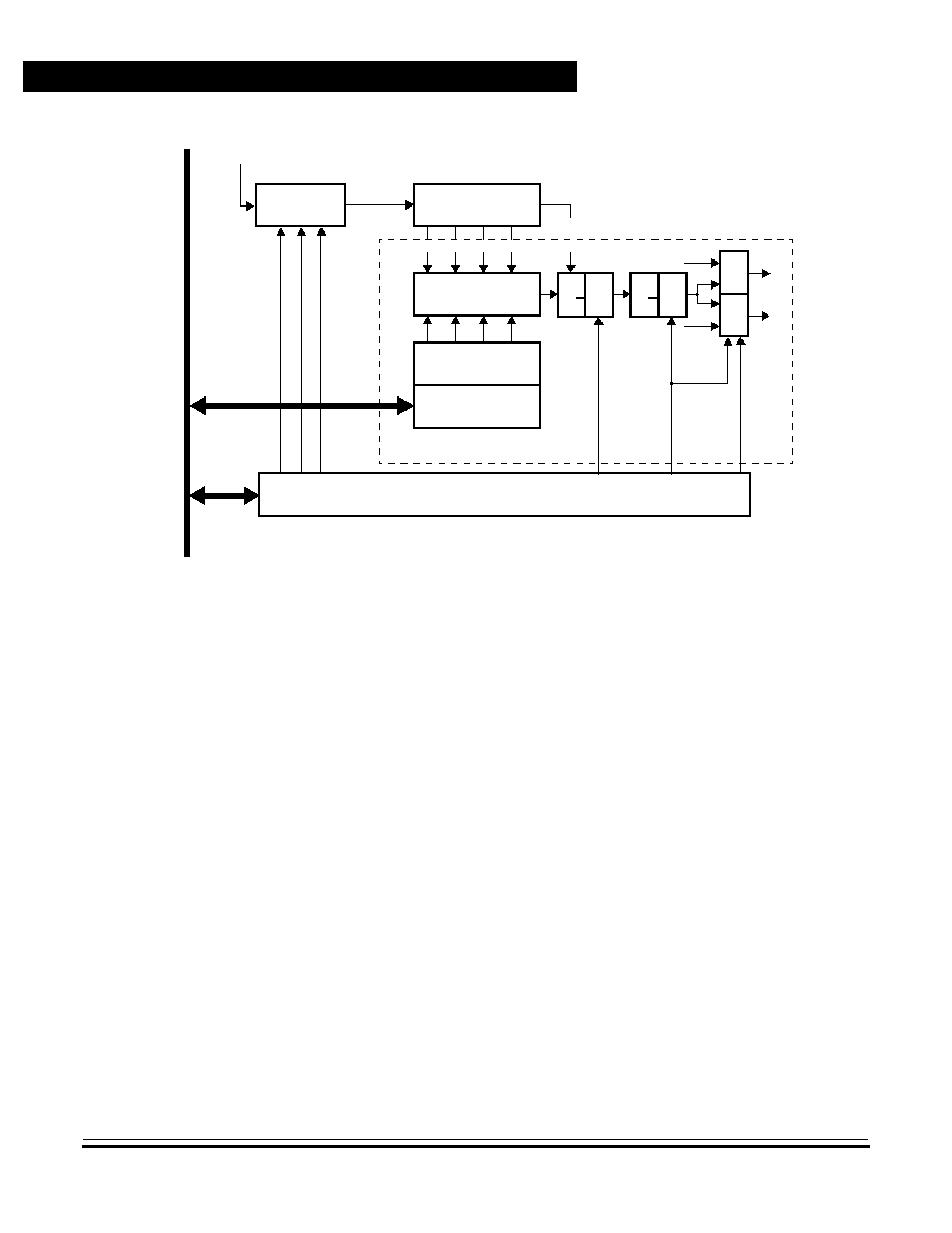
NON-DISCLOSURE AGREEMENT REQUIRED
Pulse Width Modulator (PWM)
General Release Specification
MC68HC(7)05H12
--
Rev. 1.0
160
Pulse Width Modulator (PWM)
MOTOROLA
Figure 14-1. PWM Block Diagram (one channel)
14.3 Functional Description
The PWM is capable of generating signals from 0% to 100% duty cycle.
A $00 in the PWM data register yields an `low' output (0%), but a $FF
yields a duty of 255/256. To achieve the 100% duty (`high' output), the
polarity control bit is set to zero while the data register has $00 in it.
Figure 14-1 shows the block diagram of a PWM timer channel 0 to 3.
The 8-bit counter runs at the rate of the selected clock source provided
by the programmable prescaler. The counter is compared to the data
register. When the counter matches the data register a flip-flop changes
state causing the PWM output to also change state. When the PWM
counter rolls over it resets the flip-flop and the output changes back.
Notice that there is a select bit called PPOL which allows each channel
to independently create a signal which is a low-to-high or high-to-low
transition.
f
OP
PWMC0
PWMC1
HC05 DATA BUS
PPOL
˜ 0.5,1,2,4,64
PRESCALER
8-BIT COUNTER
(
˜256)
8-BIT COMPARATOR
PWM DATA
REGISTER
BUFFER
PWM DATA
S
R
Q
Q
M
U
X
PWM CONTROL, CHANNEL ENABLE AND CHANNEL POLARITY REGISTERS
PWMC2
Q
Q
M
U
X
LEFT
RIGHT
SIGN
PWME
GPO
GPO

Pulse Width Modulator (PWM)
Functional Description
MC68HC(7)05H12
--
Rev. 1.0
General Release Specification
MOTOROLA
Pulse Width Modulator (PWM)
161
NON-DISCLOSURE AGREEMENT REQUIRED
The SIGN bit in the PWM control register selects whether the left or the
right port line (left or right path of an H-bridge) is enabled for the PWM
signal. The opposite port line drives the general purpose output value.
The SIGN bit performs also the inversion of the PWM signal. This is done
because the duty values are assumed to be 2's complement values in
the range from ≠256 to +255. A change from duty value $01FF to value
$0000 (≠1 to 0) causes a change of the current direction within the
corresponding H-bridge. This is done by changing the polarity of the
PWM signal and exchanging PWM and output port signals within the H-
bridge.
14.3.1 PWM Channel Microshifting
Switching more than one PWM channel simultaneously would cause
large currents in the corresponding power drivers of the H-bridges.
Clocking of different channels must be delayed such that only one
channel switches at a time. Therefore microshifts are introduced to
achieve a switching delay between different channels.
Figure 14-2. PWM Microshifts
7/4T
BUS CLOCK
CHANNEL 0
CHANNEL 1
CHANNEL 7
CHANNEL 2
1/4T
2/4T
BUS
BUS
BUS

NON-DISCLOSURE AGREEMENT REQUIRED
Pulse Width Modulator (PWM)
General Release Specification
MC68HC(7)05H12
--
Rev. 1.0
162
Pulse Width Modulator (PWM)
MOTOROLA
The start of the PWM period is shifted by a quarter of the period time of
the bus clock t
BUS
for the channels 0 to 7. See Figure 14-2. Inevitable
large currents due to switching of the power drivers are distributed over
a number of time slots. They do not load power supply at the same time.
14.4 Registers
Associated with the PWM system, there are eight PWM data registers,
a control/sign register, a channel enable register and a channel polarity
register. The registers can be written to and read at any time.
For updating the PWM values, the following sequence must be followed:
1. Write the corresponding SIGN bit in the PWM control register
2. Write data to the corresponding data register
Not until after the data register is written are the SIGN bits transferred
from a buffer to the SIGN register. Data written to a data register is held
in a buffer and transferred to the PWM data register at the end of a PWM
cycle. Reads of a data register will always result in the read of the PWM
data buffer and not the PWM data register.

Pulse Width Modulator (PWM)
Registers
MC68HC(7)05H12
--
Rev. 1.0
General Release Specification
MOTOROLA
Pulse Width Modulator (PWM)
163
NON-DISCLOSURE AGREEMENT REQUIRED
14.4.1 PWM Data Registers
The PWM system has eight 8-bit data registers which hold the duty cycle
for each PWM output. The data bits in these registers are set by reset.
Bit 7
6
5
4
3
2
1
Bit 0
PWM0
Read:
bit 7
bit 6
bit 5
bit 4
bit 3
bit 2
bit 1
bit 0
$0010
Write:
PWM1
Read:
bit 7
bit 6
bit 5
bit 4
bit 3
bit 2
bit 1
bit 0
$0011
Write:
PWM2
Read:
bit 7
bit 6
bit 5
bit 4
bit 3
bit 2
bit 1
bit 0
$0012
Write:
PWM3
Read:
bit 7
bit 6
bit 5
bit 4
bit 3
bit 2
bit 1
bit 0
$0013
Write:
PWM4
Read:
bit 7
bit 6
bit 5
bit 4
bit 3
bit 2
bit 1
bit 0
$0014
Write:
PWM5
Read:
bit 7
bit 6
bit 5
bit 4
bit 3
bit 2
bit 1
bit 0
$0015
Write:
PWM6
Read:
bit 7
bit 6
bit 5
bit 4
bit 3
bit 2
bit 1
bit 0
$0016
Write:
PWM7
Read:
bit 7
bit 6
bit 5
bit 4
bit 3
bit 2
bit 1
bit 0
$0017
Write:
Reset:
1
1
1
1
1
1
1
1
Figure 14-3. PWM Data Registers (PWM0≠7)
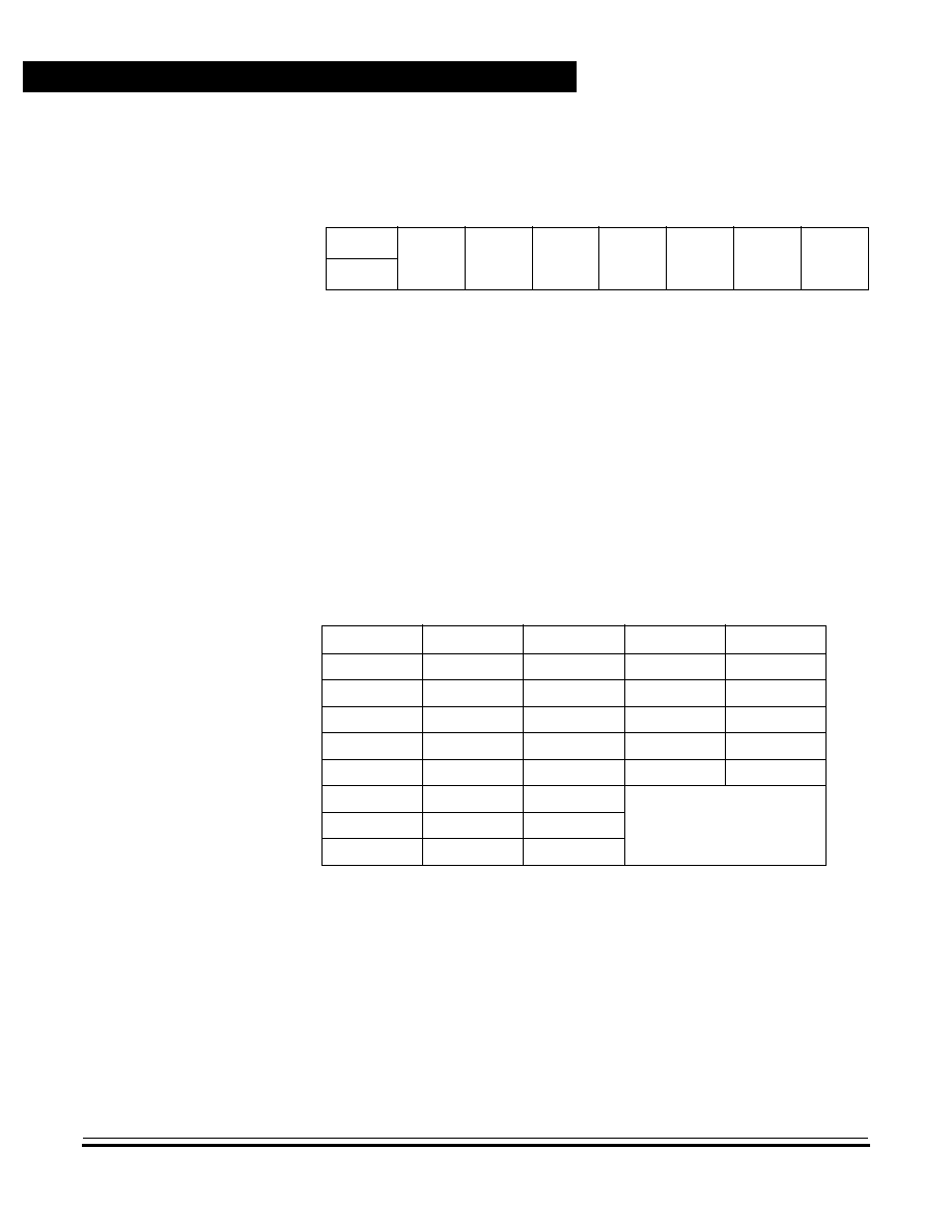
NON-DISCLOSURE AGREEMENT REQUIRED
Pulse Width Modulator (PWM)
General Release Specification
MC68HC(7)05H12
--
Rev. 1.0
164
Pulse Width Modulator (PWM)
MOTOROLA
14.4.2 PWM Control Register
PWMRST -- PWM Reset
Writing `1' to the PWMRST bit resets the PWM counter. The
PWMRST bit reads always as `0'.
PWMC3≠1 -- PWM Clock Rate
These bits select the input clock rate and determines the period as
shown in Figure 14-1. The PWM prescaler clock input is f
OP
, which is
the bus frequency.
SIGN3≠0 -- Sign of the PWM Channel 0≠3
The SIGN bit selects whether the left or the right output is the PWM
signal. The opposite output is the general purpose port. The SIGN bit
performs also the inversion of the PWM signal. See Figure 7-4 for the
assignment of the PWM channels to the power driver lines.
1 = Right PWM output
0 = Left PWM output
$0018
Bit 7
6
5
4
3
2
1
Bit 0
Read:
0
PWMC3
PWMC2
PWMC1
SIGN3
SIGN2
SIGN1
SIGN0
Write:
PWMRST
Reset:
0
1
1
1
0
0
0
0
Figure 14-4. PWM Control Register (PWMCTL)
Table 14-1. PWM Clock Rate
PWMC3
PWMC2
PWMC1
PWM Clock
PWM OUT
0
0
0
2 x f
OP
f
OP
/ 128
0
0
1
f
OP
f
OP
/ 256
0
1
0
f
OP
/ 2
f
OP
/ 512
0
1
1
f
OP
/ 4
f
OP
/ 1024
1
0
0
f
OP
/ 64
f
OP
/ 16384
1
0
1
PWM Shut off
- to save power if the PWM is
not used
1
1
0
1
1
1

Pulse Width Modulator (PWM)
Registers
MC68HC(7)05H12
--
Rev. 1.0
General Release Specification
MOTOROLA
Pulse Width Modulator (PWM)
165
NON-DISCLOSURE AGREEMENT REQUIRED
14.4.3 PWM Channel Enable Register
PWME7≠0 -- PWM Channel Enable
These bits enable/disable the corresponding PWM channels. If a bit
is disabled, the corresponding pin functions as a general purpose
output (GPO). Refer to Section 7.7 Port E and Port F (Power
Drivers).
1 = The PWM channel is enabled.
0 = The PWM channel is disabled and the corresponding lines are
general purpose outputs (GPO)
14.4.4 PWM Channel Polarity Register
PPOL7≠0 -- PWM Polarity
These bits initialize the corresponding PWM outputs.
1 = PWM channel is high at the beginning of the period, then
toggles to low when the data count is reached.
0 = PWM channel is low at the beginning of the period, then toggles
to high when the data count is reached.
$0019
Bit 7
6
5
4
3
2
1
Bit 0
Read:
PWME7
PWME6
PWME5
PWME4
PWME3
PWME2
PWME1
PWME0
Write:
Reset:
0
0
0
0
0
0
0
0
Figure 14-5. PWM Channel Enable Register (PWMEN)
$001A
Bit 7
6
5
4
3
2
1
Bit 0
Read:
PPOL7
PPOL6
PPOL5
PPOL4
PPOL3
PPOL2
PPOL1
PPOL0
Write:
Reset:
0
0
0
0
0
0
0
0
Figure 14-6. PWM Channel Polarity Register (PWMPOL)

NON-DISCLOSURE AGREEMENT REQUIRED
Pulse Width Modulator (PWM)
General Release Specification
MC68HC(7)05H12
--
Rev. 1.0
166
Pulse Width Modulator (PWM)
MOTOROLA
14.5 PWM During WAIT Mode
The PWM continues normal operation during WAIT mode. To decrease
power consumption during WAIT, the PWM should be shut off prior to
entering WAIT mode by setting the corresponding bits in the PWM
control register. Refer to Section 7.8 Port E and Port F During WAIT
Mode for information about the corresponding ports.

MC68HC(7)05H12
--
Rev. 1.0
General Release Specification
MOTOROLA
EPROM
167
NON-DISCLOSURE AGREEMENT REQUIRED
General Release Specification -- MC68HC(7)05H12
Section 15. EPROM
15.1 Contents
15.2
Introduction . . . . . . . . . . . . . . . . . . . . . . . . . . . . . . . . . . . . . . . 167
15.3
EPROM Bootloader . . . . . . . . . . . . . . . . . . . . . . . . . . . . . . . . 167
15.3.1
Bootloader Functions . . . . . . . . . . . . . . . . . . . . . . . . . . . . 168
15.4
EPROM Programming . . . . . . . . . . . . . . . . . . . . . . . . . . . . . . 170
15.4.1
EPROM Programming Register (EPROG) . . . . . . . . . . . . 170
15.5
Mask Option Register (MOR) . . . . . . . . . . . . . . . . . . . . . . . . . 171
15.2 Introduction
The HC705H12 contains 12K EPROM instead of ROM and the mask
options are controlled by a programmable nonvolatile mask option
register (MOR). The MOR is an EPROM register which must be
programmed appropriately prior to operation of the micro-controller.
15.3 EPROM Bootloader
Bootloader programming mode is entered upon the rising edge of
RESET if the IRQ/V
PP
pin is at V
TST
and the PB0 pin is at logic one (refer
to Table 6-1). The bootloader code resides in the ROM from $3F00 to
$3FEF. This program handles copying of user code from an external
EPROM into the on-chip EPROM.
The user code must be a one-to-one correspondence with the internal
EPROM addresses (including the MOR).
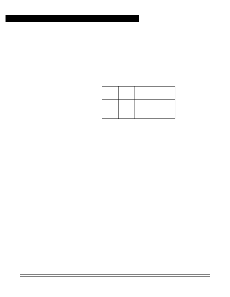
NON-DISCLOSURE AGREEMENT REQUIRED
EPROM
General Release Specification
MC68HC(7)05H12
--
Rev. 1.0
168
EPROM
MOTOROLA
15.3.1 Bootloader Functions
Two pins are used to select various bootloader functions. These pins are
PB2 and PB3. Two other pins, PB7 and PB6 are used to drive the PROG
LED and the VERF LED respectively. The programming modes are
shown in Table 15-1.
The bootloader uses an external 14 bit counter to address the memory
device containing the code to be copied. This counter requires a clock
(provided at PB5) and a reset signal (provided at PB4).
NOTE:
The EPROM must be erased before performing a program cycle.
For the communication with a host computer via a standard RS-232
interface PB1 is used as transmitter (TX) and PB0 is used as receiver
(RX).
Table 15-1. Bootloader Functions
PB2
PB3
MODE
0
0
Program/Verify EPROM
0
1
Verify only
1
0
Jump to RAM
1
1
Load RAM and Execute

EPROM
EPROM Bootloader
MC68HC(7)05H12
--
Rev. 1.0
General Release Specification
MOTOROLA
EPROM
169
NON-DISCLOSURE AGREEMENT REQUIRED
Figure 15-1. MC68HC705H12 Programming Circuit
MC74HC393
27128 (16K EPR
OM)
+5V
+5V
+5V
+5V
S2
+5V
10K
470
10K
+5V
470
S3
+5V
10K
VPP
20 pF
1MHz
L1
L2
MC68HC705H12
S1
+5V
10K
PA0
PA1
PA2
PA3
PA4
PA5
PA6
PA7
D0
D1
D2
D3
D4
D5
D6
D7
IRQ/VPP
OE
VSS
VSS
OSC2
OSC1
VDD
VREFH
AVDD
TCAP0
PB3
PB2
RESET
PB5
PB4
CLOCK
RESET
PB7
PB6
L1 ≠ VERIFY
L2 ≠ PROGRAM
A0
A1
A2
A3
A4
A5
A6
A7
A8
A9
A10
A11
A12
A13
Q0
Q1
Q2
Q3
Q4
Q5
Q6
Q7
Q8
Q9
Q10
Q11
Q12
Q13
VSS
CLK
RST
VDD
VCC
VPP
PGM
20 pF
TCAP1
TCAP2
TCAP2
CE

NON-DISCLOSURE AGREEMENT REQUIRED
EPROM
General Release Specification
MC68HC(7)05H12
--
Rev. 1.0
170
EPROM
MOTOROLA
15.4 EPROM Programming
The EPROM array is programmed through manipulation of the
programming register located at $001D. It may be programmed in user,
bootstrap or test mode. In addition to the main EPROM array, the mask
option register must also be programmed appropriately by the
programming software.
15.4.1 EPROM Programming Register (EPROG)
ELAT -- EPROM Latch Control
This read/write bit controls the latching of the address and data buses
when programming the EPROM.
1 = Address and data buses are latched when the following
instruction is a write to one of the EPROM locations. Normal
reading is disabled if ELAT =1
0 = EPROM address and data buses are configured for normal
reading
EPGM -- EPROM Program Control
This read/write bit controls whether the programming voltage is
applied to the EPROM array. For programming, this bit can only be
set if the LATCH bit has been previously set. Both EPGM and ELAT
cannot be set in the single write.
1 = Programming voltage applied to EPROM array
0 = Programming voltage not applied to EPROM array
$001D
Bit 7
6
5
4
3
2
1
Bit 0
Read:
ELAT
EPGM
Write:
Reset:
0
0
0
0
0
0
0
0
Figure 15-2. EPROM Programming Register (EPROG)

EPROM
Mask Option Register (MOR)
MC68HC(7)05H12
--
Rev. 1.0
General Release Specification
MOTOROLA
EPROM
171
NON-DISCLOSURE AGREEMENT REQUIRED
The sequence for programming the EPROM is as follows:
1. Set the ELAT bit.
2. Write the data to be programmed to the EPROM (or MOR byte)
location to be programmed.
3. Set the EPGM bit.
4. Wait a time t
EPGM
5. Clear the ELAT and EPGM bits.
6. Repeat for each byte.
15.5 Mask Option Register (MOR)
The mask option register (MOR) is used to select all mask options
available on the MC68HC705H12. When in the erased state, the
EPROM cells read as a logic zero which therefore represents the value
transferred from the MOR at reset if it is left unprogrammed. The
unimplemented bits of this register are read as `0'.
There are two mask option registers (MOR1, MOR2) implemented.
MOR2 is used only.
PWDRW -- Ports E/F in WAIT mode
1 = Ports E/F continue in WAIT (enabled)
0 = Ports E/F are forced `low' in WAIT (disabled)
COPE -- COP Timer Enable
1 = COP timer enabled.
0 = COP timer disabled.
Bit 7
6
5
4
3
2
1
Bit 0
MOR1
Read:
$3EFE
Write:
MOR2
Read:
PWDRW
COPE
$3EFF
Write:
Reset:
0
0
0
0
0
0
0
0
Figure 15-3. Mask Options Registers (MOR1 and MOR2)

NON-DISCLOSURE AGREEMENT REQUIRED
EPROM
General Release Specification
MC68HC(7)05H12
--
Rev. 1.0
172
EPROM
MOTOROLA

MC68HC(7)05H12
--
Rev. 1.0
General Release Specification
MOTOROLA
Electrical Characteristics
173
NON-DISCLOSURE AGREEMENT REQUIRED
General Release Specification -- MC68HC(7)05H12
Section 16. Electrical Characteristics
16.1 Contents
16.2
Maximum Ratings . . . . . . . . . . . . . . . . . . . . . . . . . . . . . . . . . . 174
16.3
Thermal Characteristics . . . . . . . . . . . . . . . . . . . . . . . . . . . . . 175
16.4
Power Considerations. . . . . . . . . . . . . . . . . . . . . . . . . . . . . . . 175
16.5
DC Electrical Characteristics . . . . . . . . . . . . . . . . . . . . . . . . . 176
16.6
Control Timing . . . . . . . . . . . . . . . . . . . . . . . . . . . . . . . . . . . . 178
16.7
A/D Converter Characteristics . . . . . . . . . . . . . . . . . . . . . . . . 178
16.8
EEPROM Characteristics . . . . . . . . . . . . . . . . . . . . . . . . . . . . 179
16.9
EPROM Characteristics . . . . . . . . . . . . . . . . . . . . . . . . . . . . . 180
16.10 Power Driver Characteristics . . . . . . . . . . . . . . . . . . . . . . . . . 180
16.11 Power-on Reset/Low Voltage Reset Characteristics . . . . . . . 181
NON-DISCLOSURE AGREEMENT REQUIRED
Electrical Characteristics
General Release Specification
MC68HC(7)05H12
--
Rev. 1.0
174
Electrical Characteristics
MOTOROLA
16.2 Maximum Ratings
(Voltage referenced to V
SS
)
1.
Only one output shorted for a time.
Stresses above those listed as `maximum ratings' may cause permanent
damage to the device. This is a stress rating only and functional
operation of the device at these conditions is not implied. Exposure to
maximum rating conditions for extended periods may affect device
reliability.
This device contains circuitry to protect the inputs against damage due
to high static voltages or electric fields; however, it is advised that normal
precautions be taken to avoid application of any voltage higher than
maximum-rated voltages to this high-impedance circuit. For proper
operation, it is recommended that VIN and VOUT be constrained to the
range VSS
(VIN or VOUT)
VDD. Unused inputs are connected to the
appropriate voltage level, either VSS or VDD.
Positive current flow is defined as conventional current flow into the
device. Negative current flow is defined as current flow out of the device.
Rating
Symbol
Value
Unit
Supply Voltage
V
DD
≠0.3 to +7.0
V
Supply Voltage for Power Drivers
PV
DD1,2
≠0.3 to +10.0
V
Input Voltage
Normal Operation
Monitor Mode (IRQ Pin Only)
V
IN
V
IN
V
SS
≠ 0.3 to V
DD
+ 0.3
V
SS
≠ 0.3 to 2
◊
V
DD
+ 0.3
V
V
Current Drain Per Pin
I
Omax
300
mA
Short Circuit Time for Power Drivers (PE7≠0, PF3≠0)
(note 1)
t
SC
20
ms
Operating Temperature Range
T
A
≠40 to +85
∞
C
Storage Temperature Range
T
STG
≠65 to +150
∞
C
Write/Erase Cycles EEPROM
10,000
cycles
Data Retention EEPROM
10
years

Electrical Characteristics
Thermal Characteristics
MC68HC(7)05H12
--
Rev. 1.0
General Release Specification
MOTOROLA
Electrical Characteristics
175
NON-DISCLOSURE AGREEMENT REQUIRED
16.3 Thermal Characteristics
16.4 Power Considerations
The average chip junction temperature, T
J
, in degrees Celsius can be
obtained from the following equation:
[1]
where:
T
A
= Ambient temperature (
∞
C)
JA
= Package thermal resistance, junction-to-ambient (
∞
C/W)
P
D
= P
INT
+ P
I/O
(W)
P
INT
= Internal chip power = I
DD
∑ V
DD
(W)
P
I/O
= Power dissipation on input and output pins (user determined)
An approximate relationship between P
D
and T
J
(if P
I/O
is neglected) is:
[2]
Solving equations [1] and [2] for K gives:
[3]
where K is a constant for a particular part. K can be determined by
measuring P
D
(at equilibrium) for a known T
A
. Using this value of K, the
values of P
D
and T
J
can be obtained for any value of T
A
by solving the
above equations. The package thermal characteristics are shown in
Section 16.3 Thermal Characteristics.
Characteristic
Symbol
Value
Unit
Thermal Resistance
PLCC(52 pin)
JA
50
∞
C
/
W
T
J
T
A
P
D
JA
∑
(
)
+
=
P
D
K
T
J
273
+
-----------------------
=
K
P
D
T
A
273
+
(
)
∑
JA
P
D
2
∑
+
=

NON-DISCLOSURE AGREEMENT REQUIRED
Electrical Characteristics
General Release Specification
MC68HC(7)05H12
--
Rev. 1.0
176
Electrical Characteristics
MOTOROLA
16.5 DC Electrical Characteristics
(V
DD
= 5.0Vdc
±
10%, V
SS
= 0Vdc, T
A
= ≠40
∞
C to +85
∞
C, unless otherwise noted)
Characteristic
Symbol
Min
Typ
1
Max
Unit
Output Voltage
I
LOAD
= ≠10
µ
A
I
LOAD
= +10
µ
A
V
OH
V
OL
V
DD
≠ 0.1
--
--
--
--
0.1
V
Output High Voltage
I
LOAD
= ≠0.8 mA
PA7≠0, PB7≠0, PC7≠0
I
LOAD
= ≠80
µ
A
OSC2
V
OH
V
DD
≠ 0.8
V
DD
≠ 0.8
--
--
--
--
V
V
Output Low Voltage
I
LOAD
= 1.6 mA
PA7≠0, PB7≠0, PC7≠0, RESET
I
LOAD
= 80
µ
A
OSC2
V
OL
--
--
--
--
0.4
0.4
V
V
Output Source Current (see maximum ratings)
V
O
= 4.5 V (V
DD
= 5V)
V
O
= 4.0 V (V
DD
= 5V)
PA7≠0, PB7≠0, PC7≠0
I
OH
≠1.0
≠3.0
--
--
≠14.5
≠26.0
mA
mA
Output Sink Current (see maximum ratings)
V
O
= 0.5 V (V
DD
= 5V)
V
O
= 1.0 V (V
DD
= 5V)
PA7≠0, PB7≠0, PC7≠0
I
OL
5.0
10.0
--
--
15.0
27.0
mA
mA
Input High Voltage
PA7≠0, PB7≠0, PC7≠0, PD3≠0, IRQ,
RESET, OSC1
V
IH
0.7
◊
V
DD
--
V
DD
V
Input Low Voltage
PA7≠0, PB7≠0, PC7≠0, PD3≠0, IRQ,
RESET, OSC1
V
IL
V
SS
--
0.2
◊
V
DD
V
Supply current (note 2)
Run (f
OP
= 2.1 MHz)
Run (f
OP
= 525 kHz, Slow Mode)
Wait (f
OP
= 2.1 MHz)
Wait (f
OP
= 525 kHz, Slow Mode)
IDD
IDD
IDD
IDD
--
--
--
--
7
--
3
1
10
7
6
4
mA
mA
mA
mA
IO Ports Hi-Z Leakage Current
PA7≠0, PB7≠0, PC7≠0
I
IL
--
--
±
1
µ
A
Input Current
PD3≠0, IRQ, OSC1, V
REFH
I
IN
--
--
±
1
µ
A

Electrical Characteristics
DC Electrical Characteristics
MC68HC(7)05H12
--
Rev. 1.0
General Release Specification
MOTOROLA
Electrical Characteristics
177
NON-DISCLOSURE AGREEMENT REQUIRED
1.
Typical values reflect average measurements at midpoint of voltage range at
25
∞
C.
2.
Test Conditions: All I/O Ports are configured as output with no DC load. External
Clock Input OSC1 is driven by square wave external clock.
3.
A simple protection can be built with a series resistor: R > V
MAX
/I
INJ
The sum of
currents during multiple injection should be limited below the maximum values
for a single pin: R > (V
MAX
/I
INJ
)∑(number of pins). The A/D conversion accuracy
can degrade to
±
7LSB on a channel adjacent to the one subjected to current
injection. Not production tested.
4.
The Enabling of the LVR by mask option will cause a permanent current trough
the LVR circuitry.
5.
The MCU retains RAM contents and CPU register contents.
Schmitt Trigger Inputs ≠ Hysteresis
PA7≠0, PB7≠5, PC6, PC3≠0, IRQ, RESET
V
HYRS
0.3
--
1.5
V
Internal Pullup Resistor
RESET
R
RSTPU
8
11
14
K
Injection Current (note 3)
PA7≠0
PB7≠2
PC7≠0
PD3≠0
PE7≠0
PF3≠0
I
INJ
--
--
±
10
±
10
±
10
±
1
±
10
±
10
mA
Data Retention Supply Voltage (note 5)
V
DR
2
V
Oscillator transconductance (I
OSC2
/V
OSC1
)
g
m
1.1
--
--
mA/V
Characteristic
Symbol
Min
Typ
1
Max
Unit

NON-DISCLOSURE AGREEMENT REQUIRED
Electrical Characteristics
General Release Specification
MC68HC(7)05H12
--
Rev. 1.0
178
Electrical Characteristics
MOTOROLA
16.6 Control Timing
(V
DD
= 5.0Vdc
±
10%, V
SS
= 0Vdc, T
A
= ≠40
∞
C to +85
∞
C, unless otherwise noted)
16.7 A/D Converter Characteristics
1. The minimum period tILIL should not be less than the number of cycle times it takes to execute the interrupt ser-
vice routine plus 21 t
CYC
.
(V
DD
= 5.0Vdc
±
10%, V
SS
= 0Vdc, T
A
= ≠40
∞
C to +85
∞
C, unless otherwise noted)
Characteristic
Symbol
Min
Max
Unit
Oscillator Frequency
Crystal / Ceramic Resonator
External Clock Source
f
OSC
--
dc
4.2
4.2
MHz
MHz
Internal Operating Frequency (f
OSC
/ 2)
Crystal / Ceramic Resonator
External Clock
f
OP
--
dc
2.1
2.1
MHz
MHz
Cycle Time (1 / f
OP
)
t
CYC
476
--
ns
RESET Pulse Width
t
RL
1.5
--
t
CYC
IRQ Interrupt Pulse Width Low (Edge-Triggered)
t
ILIH
120
--
ns
IRQ Interrupt Pulse Period
t
ILIL
--
(1)
--
t
CYC
OSC1 Pulse Width
t
OH
,t
OL
100
--
ns
Characteristic
Parameter
Min
Max
Unit
Resolution
Number of bits resolved by the A/D
8
--
Bit
Monotonicity
Conversion result never decreases with an
increase in input voltage and has no missing
codes
GUARANTEED
Quantization Error
Uncertainly due to converter resolution
--
±
1/2
LSB
Offset Error
DC shift of the entire transfer curve of an ideal
converter
(1)
--
±
1/2
LSB
Gain Error
Difference between the actual and expected
gain (end point to end point)
(1)
--
±
1/2
LSB
Differential Linearity Error
Difference between the actual analog voltage
change and the ideal voltage change
(1)
--
±
1/2
LSB
Integral Linearity Error
Max deviation from the best straight line
through the A/D transfer characteristics
(1)
--
±
1/2
LSB

Electrical Characteristics
EEPROM Characteristics
MC68HC(7)05H12
--
Rev. 1.0
General Release Specification
MOTOROLA
Electrical Characteristics
179
NON-DISCLOSURE AGREEMENT REQUIRED
16.8 EEPROM Characteristics
1. AVDD = V
REFH
= VDD and V
REFL
= 0 V
2. For 8-bit resolution Vref
3.5V is necessary
3. When VIN > V
REFH
Conversion result will be `FF' (for the max input voltage VIN see maximum ratings)
(V
DD
= 5.0Vdc
±
10%, V
SS
= 0Vdc, T
A
= ≠40
∞
C to +85
∞
C, unless otherwise noted)
Absolute Accuracy /
Total Unadjusted Error
Difference between the actual input voltage
and the full-scale equivalent of the binary
code output for all errors
(1)
--
±
1.5
LSB
Conversion Range
Analog input voltage range
V
SS
V
REFH
V
V
REFH
Analog reference voltage
(2)
V
SS
VDD + 0.1
V
Conversion Time
Total time to perform a single analog to digital
conversion
--
32
cycles
Zero Input Reading
Conversion result when VIN = V
SS
00
--
Hex
Full Scale Reading
(3)
Conversion result when VIN = V
REFH
--
FF
Hex
RC oscillator stabilization
time t
RCON
5
µ
s
ADC stabilization time t
ADON
100
µ
s
Characteristic
Parameter
Min
Max
Unit
Characteristic
Symbol
Min
Max
Unit
EEPROM Byte Programming Time
t
EEPGM
10
10
ms
EEPROM Byte Erase Time
t
EBYTE
10
10
ms
EEPROM Block Erase Time
t
EBLOC
10
50
ms
EEPROM Bulk Erase Time
t
EBULK
20
50
ms
RC oscillator stabilization time
t
RCON
--
5
µ
s

NON-DISCLOSURE AGREEMENT REQUIRED
Electrical Characteristics
General Release Specification
MC68HC(7)05H12
--
Rev. 1.0
180
Electrical Characteristics
MOTOROLA
16.9 EPROM Characteristics
(V
DD
= 5.0Vdc
±
10%, V
SS
= 0Vdc, T
A
= ≠40
∞
C to +85
∞
C, unless otherwise noted)
1.
Typical value = 12 ≠ 15 V.
16.10 Power Driver Characteristics
(All voltages are referenced to V
SS
, V
DD
= 5.0Vdc
±
10%, V
SS
= 0Vdc, T
A
= ≠40
∞
C to +85
∞
C,
inductive load at the Power Drivers Outputs (PE7≠0,PF3≠0): L=100 mH, R=260
)
1. The value for the supply voltage for the power driver is under normal operating conditions as well as under short
circuit conditions.
2. The power driver outputs are slew rate limited. The value show the minimal time for an inductive load (L=100 mH,
R=260
) which is connected to PVDD.
Characteristic
Symbol
Min
Max
Unit
EPROM Programming Voltage Rate
1
V
PP
V
SS
≠0.3
17.5
V
EPROM Programming Time
t
EPGM
4
-
ms
EPROM Data Retention
10
years
Characteristic
Symbol
Min
Typ
Max
Unit
Operating Supply Voltage for Power Drivers
(1)
PV
DD
V
DD
--
9.5
V
Output High Voltage
I
OH
= ≠35 mA
PE7≠0, PF3≠0
V
OH
PV
DD
≠ 0.5
--
PV
DD
+ 0.5
V
Output Low Voltage
I
OL
= +35 mA
PE7≠0, PF3≠0
V
OL
0
--
0.5
V
Output Rise Time
(2)
10% to 90% of V
OH
, PVDD = 8V, T = +25
∞
C
PE7≠0, PF3≠0
t
r
21
--
--
ns
Output Fall Time (note 2)
90% to 10% of V
OH
, PVDD = 8V, T = +25
∞
C
PE7≠0, PF3≠0
t
f
19
--
--
ns

Electrical Characteristics
Power-on Reset/Low Voltage Reset Characteristics
MC68HC(7)05H12
--
Rev. 1.0
General Release Specification
MOTOROLA
Electrical Characteristics
181
NON-DISCLOSURE AGREEMENT REQUIRED
16.11 Power-on Reset/Low Voltage Reset Characteristics
(V
DD
= 5.0Vdc
±
10%, V
SS
= 0Vdc, T
A
= ≠40
∞
C to +85
∞
C, unless otherwise noted)
1. Typical values reflect average measurements at midpoint of voltage range at 25
∞
C.
Characteristic
Symbol
Min
Typ
(1)
Max
Unit
Low Voltage Reset (LVR) ≠ Threshold
Voltage
V
RON
≠ (VDD Increasing)
V
ROFF
≠ (VDD Decreasing)
Hysteresis
V
RON
V
ROFF
V
HYST
3.4
3.3
0.1
3.85
3.75
--
4.3
4.2
--
V
V
V
Minimum Reset Voltage
V
min
1.0
--
--
V
Supply Voltage Rise and Fall Time
--
--
--
1000
ms
Low Voltage Reset Internal Delay Time
--
--
5
--
ms

NON-DISCLOSURE AGREEMENT REQUIRED
Electrical Characteristics
General Release Specification
MC68HC(7)05H12
--
Rev. 1.0
182
Electrical Characteristics
MOTOROLA

MC68HC(7)05H12
--
Rev. 1.0
General Release Specification
MOTOROLA
Mechanical Specifications
183
NON-DISCLOSURE AGREEMENT REQUIRED
General Release Specification -- MC68HC(7)05H12
Section 17. Mechanical Specifications
17.1 Contents
17.2
Pin Assignments . . . . . . . . . . . . . . . . . . . . . . . . . . . . . . . . . . . 184
17.3
Package Dimensions . . . . . . . . . . . . . . . . . . . . . . . . . . . . . . . 184
17.2 Pin Assignments
Figure 17-1. 52-Pin PLCC Pin Assignments
40
46
8
14
21
27
7
1
47
34
20
33
VREFH
AVDD
VDD
PC0/TCAP0
PC1/TCAP1
PC2/TCAP2
PC3/TCAP3
PC4/TCMP0
PC5/TCMP1
PC6/RDI
PC7/TDO
PVDD2
PVSS2
PE7
PE6
PE5
PE4
PF3
PF2
PF1
PF0
PE3
PE2
PE1
PE0
PVSS1
PB3
PB2/ECLK
PB1
PB0
PA7
PA6
PA5
PA4
PA3
PA2
PA1
PA0
PVDD1
PD3/AN3
PD2/AN2
PD1/AN1
PD0/AN0
VSS
RESET
OSC1
OSC2
IRQ
/VPP
PB7/SCK
PB6/MOSI
PB5/MISO
PB4

NON-DISCLOSURE AGREEMENT REQUIRED
Mechanical Specifications
General Release Specification
MC68HC(7)05H12
--
Rev. 1.0
184
Mechanical Specifications
MOTOROLA
17.3 Package Dimensions
Figure 17-2. 52-Pin PLCC Package Dimensions
≠L≠
≠M≠
≠P≠
≠N≠
pin 1
pin 52
V
W
Y BRK
Z
R
A
C
J E
G
G1
U
B
G1
Z1
X
0.10
≠T≠
SEATING PLANE
0.18
T N
≠P
L
≠M
M
S
S
S
S
Case No. 778-02
52 Lead PLCC
Dim.
Min.
Max.
Notes
Dim.
Min.
Max.
A
19.94
20.19
1. Datums ≠L≠, ≠M≠, ≠N≠ and ≠P≠ are determined where top of lead
shoulder exits plastic body at mould parting line.
2. Dimension G1, true position to be measured at datum ≠T≠ (seating
plane).
3. Dimensions R and U do not include mould protrusion. Allowable
mould protrusion is 0.25mm per side.
4. Dimensions and tolerancing per ANSI Y 14.5M, 1982.
5. All dimensions in mm.
U
19.05
19.20
B
19.94
20.19
V
1.07
1.21
C
4.20
4.57
W
1.07
1.21
E
2.29
2.79
X
1.07
1.42
F
0.33
0.48
Y
--
0.50
G
1.27 BSC
Z
2
∞
10
∞
H
0.66
0.81
G1
18.04
18.54
J
0.51
--
K1
1.02
--
K
0.64
--
Z1
2
∞
10
∞
R
19.05
19.20
0.18
T L
≠M
N
≠P
M
S
S
S
S
0.18
T L
≠M
N
≠P
M
S
S
S
S
0.18
T N
≠P
L
≠M
M
S
S
S
S
0.25
T L
≠M
N
≠P
S
S
S
S
S

MC68HC(7)05H12
--
Rev. 1.0
General Release Specification
MOTOROLA
Index
185
General Release Specification -- MC68HC(7)05H12
Index
16-bit timer
block diagram
104
interrupts
64
register addresses
105
52-pin PLCC case outline
184
52-pin PLCC package
20
,
183
8-bit timer
see core timer
A
A/D
channel assignments
147
clock selection
147
conversion accuracy
150
data register (ADDR)
148
electrical characteristics
178
errors
151
status and control register (ADSCR)
146
,
147
accumulator
39
address mark wake-up
131
addressing modes
42
ADON bit in ADSCR
146
ADRC bit in ADSCR
146
ALU -- arithmetic/logic unit
42
AN0≠AN3
23
analog input
148
analog to digital converter
see A/D
AVDD
21
B
bit manipulation instructions
50
block diagrams
16-bit timer
104
core timer
98
MC68HC(7)05H12
19
PWM
160
SCI
128
SPI
119
bootloader
167
C
carry/borrow flag
41
C-bit in CCR
41
CH3_0 bits in ADSCR
147
channel microshifting
161
CO2E bit in TCR2
112
COCO bit in ADSCR
146
COIE bit in TCR1
111
condition code register (CCR)
40
control instructions
51
control timing
178
COP
register (COPR)
72
reset
70
,
101
COPE bit in MOR
171
COPR bit in COPR
72
core timer
block diagram
98
counter register (CTCR)
101
interrupts
64

MC68HC(7)05H12
--
Rev. 1.0
General Release Specification
MOTOROLA
Index
186
Index
status and control register (CTSCR)
99
counter
105
CPHA bit in SPCR
122
CPOL bit in SPCR
122
cross coupled coils
85
D
data retention mode
78
DC electrical characteristics
176
differential linearity error
151
direct addressing mode
43
DOD bit in SPCR
121
E
ECLK bit in SYSCR
34
ECLK pin
22
EDGE7≠0 bits in PAIED
81
EELAT bit in EEPCR
155
EEOSC bit in EEPCR
154
EEPGM bit in EEPCR
155
EEPROM
35
control register (EEPCR)
154
,
155
electrical characteristics
179
erase
156
options register (EEOPR)
155
,
156
programming
157
read
156
EEPRT bit in EEOPR
156
EER1, EER0 bits in EEPCR
154
ELAT bit in EPROG
170
EPGM bit in EPROG
170
EPROM
35
bootloader
167
electrical characteristics
180
programming
170
programming register (EPROG)
170
erase mode select
154
extended addressing mode
43
external interrupt
63
F
FE bit in SCSR
139
features
18
flowcharts
interrupt
62
WAIT
77
G
gain scale error
151
H
half-carry flag
41
hardware interrupts
63
≠
65
H-bit in CCR
41
H-bridge
driver
86
states
90
with the PWM
94
I
I/O programming
95
IC1F bit in TSR
113
IC2F bit in TSR
113
ICI1E bit in TCR1
111
ICI2E bit in TCR1
111
IDLE bit in SCSR
139
idle line wake-up
131
IEDG1 bit in TCR1
111
IEDG2 bit in TCR1
111
ILIE bit in SCCR2
137
illegal address reset
72
immediate addressing mode
43
index register
39
indexed addressing mode
44

MC68HC(7)05H12
--
Rev. 1.0
General Release Specification
MOTOROLA
Index
187
Index
inherent addressing mode
43
input capture
register 1
108
register 2
109
instruction types
45
integral linearity error
151
interrupts
16-bit timers
64
core timer
64
flowchart
62
hardware
63
IRQ
63
keyboard
63
SCI
65
SPI
65
SWI
63
IRQ bit in SYSCR
34
IRQ pin
21
J
jump/branch instructions
48
junction temperature, chip
175
K
keyboard interrupt
22
,
63
,
80
L
low power modes
65
,
76
low voltage reset (LVR)
72
electrical characteristics
181
M
M bit in SCCR1
136
mask options
20
register (MOR)
171
master mode
120
maximum ratings
174
memory map
26
MISO
22
,
116
modes of operation
data retention
78
entry conditions
75
low power (WAIT)
65
,
76
≠
78
monitor
76
slow
78
user
75
monitor mode
76
monitor ROM
35
monotonicity
150
MOR
171
MOSI
22
,
117
MSTR bit in SPCR
121
N
N-bit in CCR
41
negative flag
41
NF bit in SCSR
139
O
OC1F bit in TSR
113
OC2F bit in TSR
114
OCI1E bit in TCR1
111
OCI2E bit in TCR2
112
offset error
151
OLVL1 bit in TCR1
111
OLVL2 bit in TCR2
112
opcode map
58
operating modes
see modes of operation
OR bit in SCSR
139
OSC1, OSC2
21
oscillator pins
21
output compare
106

MC68HC(7)05H12
--
Rev. 1.0
General Release Specification
MOTOROLA
Index
188
Index
register 1
106
register 2
107
P
PA0≠PA7
22
PAIE7≠0 bits in PAICR
81
PAIF7≠0 bits in PAISR
82
PB0≠PB7
22
PC0≠PC7
22
PD0≠PD3
23
PE0≠PE7
23
PF0≠PF3
23
pins
AN0≠AN3
23
assignments
20
AVDD
21
ECLK
22
IRQ
21
keyboard interrupt
22
MISO
22
MOSI
22
OSC1, OSC2
21
port A (PA0≠PA7)
22
port B (PB0≠PB7)
22
port C (PC0≠PC7)
22
port D (PD0≠PD3)
23
port E (PE0≠PE7)
23
port F (PF0≠PF3)
23
PVDD1, PVSS1, PVDD2, PVSS2
23
RDI
22
RESET
21
SCK
22
TCAP0≠3
22
TCMP0≠1
22
TDO
22
VDD, VSS
21
VPP
21
VREFH
23
port A
interrupt control register (PAICR)
81
interrupt edge register (PAIED)
81
interrupt status register (PAISR)
82
keyboard interrupt
80
port B
82
port C
83
port D
83
port E and port F
configurations
92
mismatch registers (PEMISM and PFMISM)
89
,
90
power drivers
83
power considerations
175
power driver
circuit
87
electrical characteristics
180
pins
23
,
83
power supply pins
21
power-on reset (POR)
70
electrical characteristics
181
PPOL7≠0 bits in PWMPOL
165
program counter
40
programming circuit
169
programming model
38
pulse width modulator
see PWM
PVDD1, PVSS1, PVDD2, PVSS2
23
PWDRW bit in MOR
171
PWM
block diagram
160
channel enable register (PWMEN)
165
channel microshifting
161
channel polarity register (PWMPOL)
165
control register (PWMCTL)
164
data registers (PWM0≠7)
163
PWMC3≠1 bits in PWMCTL
164
PWME7≠0 bits in PWMEN
165

MC68HC(7)05H12
--
Rev. 1.0
General Release Specification
MOTOROLA
Index
189
Index
PWMRST bit in PWMCTL
164
Q
quantization error
151
R
R8 bit in SCCRI
136
RAM
35
RCKB bit in BAUD
141
RDI
22
RDRF bit in SCSR
139
RE bit in SCCR2
138
read-modify-write instructions
47
receive data (RDI)
132
receiver
130
register/memory instructions
46
registers
ADDR
148
ADSCR
146
BAUD
140
complete listing
29
≠
33
COPR
72
CTCR
102
CTSCR
99
EEOPR
155
EEPCR
154
EPROG
170
MOR
171
PAICR
81
PAIED
81
PAISR
82
PEMISM
89
PFMISM
90
PWM07
163
PWMCTL
164
PWMEN
165
PWMPOL
165
SCCR1
136
SCCR2
137
SCDAT
135
SCSR
138
SPCR
121
SPDAT
124
SPSR
123
summary
27
SYSCR
34
TCR1
110
TCR2
112
TSR
113
relative addressing mode
45
RESET
21
,
67
resets
computer operating properly (COPR)
70
external
67
illegal address
72
internal
68
LVR
72
POR
70
RESET
67
RIE bit in SCCR2
137
ROM
35
RRTIF bit in CTSCR
100
RT1, RT0 bits in CTSCR
100
RTI rates
100
RTIE bit in CTSCR
100
RTIF bit in CTSCR
99
RTOF bit in CTSCR
100
RWU bit in SCCR2
138
S
SBK bit in SCCR2
138
SC bit in SYSCR
34
SCI
baud rate register (BAUD)
140
,
141
block diagram
128

MC68HC(7)05H12
--
Rev. 1.0
General Release Specification
MOTOROLA
Index
190
Index
control register 1 (SCCR1)
136
control register 2 (SCCR2)
137
,
138
data format
130
data register (SCDAT)
135
interrupt
65
receiver wake-up
130
status register (SCSR)
138
,
139
SCK
22
,
117
SCP1, SCPO bits in BAUD
141
SCR2, SCR1, SCRO bits in BAUD
141
serial communcations interface
see SCI
serial peripheral interface
see SPI
short circuit detection
88
SIGN3≠0 bits in PWMCTL
164
slave mode
120
slow mode
78
software interrupt (SWI)
63
SPE bit in SPCR
121
SPI
block diagram
119
control register (SPCR)
121
,
122
data I/O register (SPDAT)
124
interrupt
65
master and slave
120
MISO
116
MOSI
117
serial clock (SCK)
117
status register (SPSR)
123
SPIE bit in SPCR
121
SPIF bit in SPSR
123
SPP bit in BAUD
140
SPR1, SPR0 bits in SPCR
122
stack pointer
39
start bit
132
system control register (SYSCR)
34
ECLK -- internal system clock available
34
IRQ -- IRQ sensitivity
34
SC -- system clock option
34
T
T8 bit in SCCR1
136
TC bit in SCSR
139
TCAP0≠3
22
TCAP1 bit in TSR
113
TCAP2 bit in TSR
113
TCIE bit in SCCR2
137
TCLR bit in BAUD
140
TCMP0≠1
22
TDO
22
TDRE bit in SCSR
139
TE bit in SCCR2
137
thermal characteristics
175
TIE bit in SCCR2
137
timer control register 1 (TCR1)
110
CO1E -- timer compare 1 output enable
111
ICI1E -- input capture 1 interrupt enable
111
ICI2E -- input capture 2 interrupt enable
111
IEDG1 -- input edge
111
IEDG2 -- input edge
111
OCI1E -- output compare 1 interrupt enable
111
OLVL1 -- output level 1
111
TOIE -- timer overflow interrupt enable
111
timer control register 2 (TCR2)
112
CO2E -- timer compare 2 output enable
112
OCI2E -- output compare 2 interrupt enable
112
OLVL2 -- output level 2
112
timer status register (TSR)
113
IC1F -- input capture 1 flag
113
IC1F -- output compare 1 flag
113
IC2F -- input capture 2 flag
113
IC2F -- output compare 2 flag
114
TCAP1 -- timer capture 1
113

MC68HC(7)05H12
--
Rev. 1.0
General Release Specification
MOTOROLA
Index
191
Index
TCAP2 -- timer capture 2
113
TOF -- timer overflow flag
113
timing diagrams
data clock
118
RESET and POR
69
TOF bit in CTSCR
99
TOF bit in TSR
113
TOFE bit in CTSCR
100
TOIE bit in TCR1
111
total unadjusted error
151
transfer curve
150
transmit data (TDO)
135
U
user mode
75
V
VDD, VSS
21
vector addresses
61
VPP
21
VREFH
23
W
WAIT mode
65
,
77
WAKE bit in SCCR1
136
wake-up
130
address mark
131
idle line
131
watchdog
see COP
WCOL bit in SPSR
123
Z
Z-bit in CCR
41
zero flag
41

MC68HC(7)05H12
--
Rev. 1.0
General Release Specification
MOTOROLA
Index
192
Index


HC05H12GRS/D
Motorola reserves the right to make changes without further notice to any products herein. Motorola makes no warranty, representation or guarantee regarding the suitability of its
products for any particular purpose, nor does Motorola assume any liability arising out of the application or use of any product or circuit, and specifically disclaims any and all liability,
including without limitation consequential or incidental damages. "Typical" parameters which may be provided in Motorola data sheets and/or specifications can and do vary in different
applications and actual performance may vary over time. All operating parameters, including "Typicals" must be validated for each customer application by customer's technical experts.
Motorola does not convey any license under its patent rights nor the rights of others. Motorola products are not designed, intended, or authorized for use as components in systems
intended for surgical implant into the body, or other applications intended to support or sustain life, or for any other application in which the failure of the Motorola product could create a
situation where personal injury or death may occur. Should Buyer purchase or use Motorola products for any such unintended or unauthorized application, Buyer shall indemnify and hold
Motorola and its officers, employees, subsidiaries, affiliates, and distributors harmless against all claims, costs, damages, and expenses, and reasonable attorney fees arising out of,
directly or indirectly, any claim of personal injury or death associated with such unintended or unauthorized use, even if such claim alleges that Motorola was negligent regarding the
design or manufacture of the part. Motorola and
are registered trademarks of Motorola, Inc. Motorola, Inc. is an Equal Opportunity/Affirmative Action Employer.
How to reach us:
USA/EUROPE/Locations Not Listed: Motorola Literature Distribution; P.O. Box 5405; Denver, Colorado 80217.1-800-441-2447 or
303-675-2140
MfaxTM: RMFAX0@email.sps.mot.com ≠ TOUCHTONE 602-244-6609
INTERNET: http://www.mot.com/SPS/
JAPAN: Nippon Motorola Ltd.; Tatsumi-SPD-JLDC, 6F Seibu-Butsuryu-Center, 3-14-2 Tatsumi Koto-Ku, Tokyo 135, Japan.
81-3-3521-8315
ASIA/PACIFIC: Motorola Semiconductors H.K. Ltd.; 8B Tai Ping Industrial Park, 51 Ting Kok Road, Tai Po, N.T., Hong Kong. 852-26629298
Mfax is a trademark of Motorola, Inc.
©
Motorola, Inc., 1997