 | –≠–ª–µ–∫—Ç—Ä–æ–Ω–Ω—ã–π –∫–æ–º–ø–æ–Ω–µ–Ω—Ç: P32P4911A | –°–∫–∞—á–∞—Ç—å:  PDF PDF  ZIP ZIP |
Document Outline
- GENERAL DESCRIPTION
- FEATURES
- General
- Automatic Gain Control
- Filter/Equalizer
- Pulse Qualification
- Time Base Generator
- Data Separator
- Servo
- BLOCK DIAGRAM
- FUNCTIONAL DESCRIPTION
- AGC Circuit Description
- AGC Control Modes
- Pulse Qualification Circuit Descriptions
- Programmable Filter Circuit Description
- Internal AC Coupling
- Amplitude Asymmetry Detection and Correction
- Adaptive Equalizer Circuit Description
- Time Base Generator Circuit Description
- Data Separator Circuit Description
- ENDEC
- Servo Demodulator Circuit Description
- Servo Timing Outputs
- Description of Operating Modes
- Mode Control
- Power Down Operation
- REGISTER DESCRIPTIONS
- Serial Port Register Definitions
- PIN DESCRIPTIONS
- Power Supply Pins
- Analog Input Pins
- Analog Output Pins
- Analog Control Pins
- Digital Input Pins
- Digital Bi-directional Pins
- Digital Output Pins
- Serial Port Pins
- ELECTRICAL SPECIFICATIONS
- Absolute Maximum Ratings
- Recommended Operating Conditions
- Power Supply Current and Power Dissipation
- Analog Inputs
- Digital Inputs
- Digital Outputs
- Serial Port Timing
- AGC Characteristics
- AGC Control Section
- Pulse Qualifier Characteristics
- Programmable Filter Characteristics
- Transversal Filter Characteristics
- Time Base Generator Characteristics
- DATA SEPARATOR CHARACTERISTICS
- Read Mode - Byte-Wide
- Write Mode - Byte-Wide
- Write Data Output
- Read Mode - Nibble
- Write Mode - Nibble
- Write Precompensation
- Data Synchronizer PLL
- Servo Characteristics
- DAC Differential Non-Linearity
- PACKAGE OUTLINE
- DEFINITIONS
- LIFE SUPPORT APPLICATIONS

DATA SHEET
Product Specification
1996 Jul 25
INTEGRATED CIRCUITS
P32P4911A
PRML Read Channel with PR4,
8/9 ENDEC, FWR Servo

1996 Jul 25
2
853-1850 17093
Philips Semiconductors
Product specification
PRML Read Channel with PR4,
8/9 ENDEC, FWR Servo
P32P4911A
GENERAL DESCRIPTION
The Philips Semiconductors P32P4911A is a high performance BiCMOS read channel IC that provides all of the
functions needed to implement an entire Partial Response Class 4 (PR4) read channel for zoned recording hard disk
drive systems with data rates from 42 to 125 Mbit/s or 33 to 100 Mbit/s. Functional blocks include AGC, programmable
filter, adaptive transversal filter, Viterbi qualifier, 8,9 GCR ENDEC, data synchronizer, time base generator, and FWR
servo.
Programmable functions such as data rate, filter cutoff, filter boost, etc., are controlled by writing to the serial port
registers so no external component changes are required to change zones.
The part requires a single +5V power supply. The Philips Semiconductors P32P4911A utilizes an advanced BiCMOS
process technology along with advanced circuit design techniques which result in high performance devices with low
power consumption.
FEATURES
General:
∑
Register programmable data rates from 42 to 125 Mbit/s or 33 to 100 Mbit/s
∑
Sampled data read channel with Viterbi qualification
∑
Programmable filter for PR4 equalization
∑
Five tap transversal filter with adaptive PR4 equalization
∑
8/9 GCR ENDEC
∑
Data Scrambler/Descrambler
∑
Presettable Precoder State
∑
Programmable write precompensation
∑
Low operating power (0.925 W typical at 5V)
∑
Register programmable power management (<5 mW power down mode)
∑
4-bit nibble and byte-wide bi-directional NRZ data interfaces
∑
8-bit Direct Write mode automatically configured for RCLK = VCO/8
∑
Serial interface port for access to internal program storage registers
∑
Single power supply (5V
±
10%)
∑
Small footprint, 100-lead LQFP package
1996 Jul 25
3
Philips Semiconductors
Product specification
PRML Read Channel with PR4,
8/9 ENDEC, FWR Servo
P32P4911A
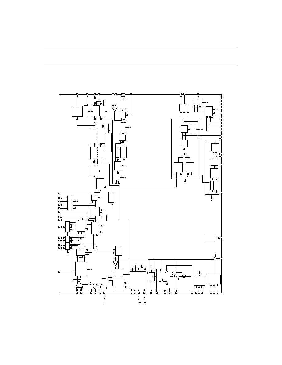
BLOCK DIAGRAM
SM00061
Philips Semiconductors P32P491
1A
DSCLK
SSBYP
VIA+
VIA≠
ON+
ON≠
OD+
OD≠
CP
CN
DP
DN
LEVEL
OR
HYSTERESIS
PULSE
QUAL
P
ARALLEL
INTERF
ACE
BYP
HOLD
LOWZ
F
ASTREC
CONV
AGC
CHARGE
PUMP
MUX
TEST
POINY
MUX
DECISION
DIRECTED
PHASE
DETECT
OR
CHARGE
PUMP
CODE WORD
BOUNDR
Y
DETECT
OR
DAMPING
CONTROL
RCLK
SBD
NRZ0≠7
NRZP
VCO SYNC
P
A
TTERN
GEN
WRITE
PRECOMP
WD
WD
DWR
DWI
DWI
WCLK
MUX
MUX
SG
POWER
DOWN
CONTROL
SDEN
SCLK
SDA
T
A
BYPS
P
ARALLEL
T
O
SERIAL
MUX
DA
T
A SYNCHRONIZER
RG
WG/WG
A
T
O
DSCLK
DSCLK
1/(N+1)
1/(M+1)
TIME BASE GENERA
T
OR
RCLK
RCLK
SYNC
FIELD
COUNTER
T
o SFC
TBGOUT
CWBD
CWBD
WRITE
FLIP-FLOP
TBGOUT
CHANQUAL
CHANQUAL
TBGOUT
ASYMM F
ACT
OR
LOW
ASYMM F
ACT
OR
DACs
SG
SQUELCH
VMIN
SFC
DC
OFFSET
CANCEL
LOWZ
SFC
TPD
MUX
EN
AGCRST
UFDC
VCC
AGCDEL
WRDEL
LZT
O
FDT
O
HOLD
HOLD
LOWZ
SQUELCH
UFDC
SFC
MAXREF/2
SER
VO
F
ASTREC
DUAL
"OR" TYPE
SYNC BYTE
DETECT
OR
P
ARITY
GEN/CHK
FULL
W
A
VE
RECTIFIER
VITERBI
DETECT
OR
5≠T
AP
EQUALIZER
2-ADAPTIVE
2-PROG
AGC
CONTROL
LOGIC
SAMPLED
AGC
CHARGE
PUMP
PROGRAMMABLE
7TH-ORDER
LOW
-P
ASS
FIL
TER
ASYMMETRIC 0'S
SERIAL
POR
T
&
CONTROL
REGISTERS
AUT
OMA
TIC
TRAINING & SYNC BYTE
GENERA
T
OR
DESCRAMBLER
SCRAMBLER
PRECODER
9,8
((0,4/4)
DECODER
A
T
O
TEST
MUX
RCLK
CLOCK
GEN
AGC
AMP
DAC
FROM LEVEL
QUAL
VCO
VCO
CONTROL
LOGIC
2≠BR
DAC
AGCREF
VRC
SREF
SDIEN
SEROUT
VP
A
VP
A
SG
0.2V
2.3V WR
T
VP
A
REFERENCE
SEL
VRC
3.2V
REFERENCE
NCLK
TPC
MUX
TPE
MUX
P
ARALLEL
T
O
SERIAL
9,8
((0,4/4)
ENCODER
NIBBLE
INTERF
ACE
CHARGE
PUMP
PHASE/
FREQ
DETECT
OR
PHASE/
FREQ
DETECT
OR
VRDT
TPB≠
TPB+
TPA≠
TPA+
EQHOLD
PPOL
RDS/RDS
TPE
TPC≠
TPC+
TPD≠
TPD+
VRX
UFDC
FASTREC
LOWZ
SFWR
AGND3
AGND2
AGND1
DGND2
DGND1
PDWN
VPA3
VPA2
VPA1
VPD2
VPD1
FLTR2≠
FLTR2+
FLTR1≠
FLTR1+
RR
FREF
MAXREF
TPE

1996 Jul 25
4
Philips Semiconductors
Product specification
PRML Read Channel with PR4,
8/9 ENDEC, FWR Servo
P32P4911A
Automatic Gain Control:
∑
Dual mode AGC, analog during acquisition, sampled during data reads
∑
Separate AGC level storage pins for data and servo
∑
Dual rate attack and decay charge pump for rapid AGC recovery (analog)
∑
Programmable, symmetric, charge pump currents for data reads (sampled)
∑
Charge pump currents track programmable data rate during data reads (sampled)
∑
Low drift AGC hold circuitry
∑
Low-Z circuitry at AGC input provides for rapid external coupling capacitor recovery
∑
AGC Amplifier squelch during Low-Z
∑
Wide bandwidth, precision full-wave rectifier
∑
Programmable AGC controls
≠ Separate external input pins for AGC hold, fast recovery, and Low-Z control
or
≠ Internal Low-Z and fast decay timing for rapid transient recovery and AGC acquisition. Timing set with external
resistors (2). Ultra fast decay current set with external resistor. AGC input impedance vs LOWZ = 5:1.
∑
2-bit DAC to control AGC voltage in servo mode between 1.1 and 1.4 V
Filter/Equalizer:
∑
Programmable, 7-pole, continuous time filter provides:
≠ Channel filter and pulse slimming equalization for equalization to PR4
≠ Programmable cutoff frequency from 4 to 34 MHz
≠ Programmable boost /equalization of 0 to 13 dB
≠ Programmable "zeros" equalization provides time asymmetry compensation
≠
±
0.5 ns group delay variation from 0.3c to c, with c = 34 MHz
≠ Minimizes size and power
≠ Low-Z switch at filter output for fast offset recovery
≠ No external coupling capacitors required
≠ DC offset compensation provided at filter output
≠ Five tap transversal filter for fine equalization to PR4
≠ Self adapting inner taps (symmetric)
≠ Programmable outer taps (symmetric, 4-bits)
≠ Equalization hold input
≠ "Zeros" channel quality output
≠ Amplitude asymmetry factor output
Pulse Qualification:
∑
Sampled Viterbi qualification of signal equalized to PR4
∑
Register programmable window or hysteresis pulse qualifier for servo reads
∑
Selectable RDS pulse width and polarity for servo gray code reads

1996 Jul 25
5
Philips Semiconductors
Product specification
PRML Read Channel with PR4,
8/9 ENDEC, FWR Servo
P32P4911A
Time Base Generator:
∑
Less than 1% frequency resolution
∑
Up to 141 MHz frequency output
∑
Independent M and N divide-by registers
∑
No active external components required
Data Separator:
∑
Fully integrated data separator includes data synchronizer and 8,9 GCR ENDEC
∑
Register programmable to 125 Mbit/s operation
∑
Fast Acquisition, sampled data phase lock loop
∑
Decision directed clock recovery from data samples
∑
Adaptive clock recovery thresholds
∑
Programmable damping ratio for data synchronizer PLL is constant for all data rates
∑
Data scrambler/descrambler to reduce fixed pattern effects
∑
4-bit nibble and byte-wide NRZ data interfaces
∑
Nibble clock is available during byte-wide mode
∑
Time base tracking, programmable write precompensation
∑
Differential PECL write data output
∑
Integrated sync byte detection, single byte or dual ("or" type)
∑
Semi-auto training and sync byte generation available for single sync byte operation
∑
Surface defect scan mode
Servo:
∑
Wide bandwidth, precision full-wave rectifier
∑
Separate, automatically selected, registers for servo c, boost, and threshold
∑
SEROUT and SREF pins to provide a differential full-wave rectified servo signal
∑
SELVRC and SDIEN control pins for dc gain and offset calibration
∑
AGCREF output to provide 2-bit DAC-controlled voltage for applications requiring a fixed gain in servo mode