
INTEGRATED CIRCUITS
DATA SHEET
Product specification
File under Integrated Circuits, IC20
1999 Mar 12
P8xC557E8
8-bit microcontroller

1999 Mar 12
2
Philips Semiconductors
Product specification
8-bit microcontroller
P8xC557E8
CONTENTS
1
FEATURES
2
GENERAL DESCRIPTION
2.1
Electromagnetic Compatibility (EMC)
2.2
Recommendation on ALE
3
ORDERING INFORMATION
4
BLOCK DIAGRAM
5
FUNCTIONAL DIAGRAM
6
PINNING INFORMATION
6.1
Pinning diagram
6.2
Pin description
7
FUNCTIONAL DESCRIPTION
8
MEMORY ORGANIZATION
8.1
Program Memory
8.2
Internal Data Memory
8.3
Addressing
9
I/O FACILITIES
10
PULSE WIDTH MODULATED OUTPUTS
(PWM)
10.1
Prescaler Frequency Control Register (PWMP)
10.2
Pulse Width Register 0 (PWM0)
10.3
Pulse Width Register 1 (PWM1)
11
ANALOG-TO-DIGITAL CONVERTER (ADC)
11.1
ADC features
11.2
ADC functional description
11.3
ADC timing
11.4
ADC configuration and operation
11.5
ADC during Idle and Power-down mode
11.6
ADC resolution and characteristics
11.7
ADC after reset
11.8
ADC Special Function Registers
12
TIMERS/COUNTERS
12.1
Timer 0 and Timer 1
12.2
Timer T2
12.3
Watchdog Timer T3
13
SERIAL I/O PORTS
13.1
Serial I/O Port: SIO0 (UART)
13.2
Serial I/O Port: SIO1 (I
2
C-bus interface)
14
INTERRUPT SYSTEM
14.1
Interrupt Enable Registers
14.2
Interrupt Handling
14.3
Interrupt Priority Structure
14.4
Interrupt vectors
14.5
Interrupt Enable and Priority Registers
15
POWER REDUCTION MODES
15.1
Idle mode
15.2
Power-down mode
15.3
Wake-up from Power-down mode
15.4
Status of external pins
15.5
Power Control Register (PCON)
16
OSCILLATOR CIRCUITS
16.1
XTAL1; XTAL2 oscillator: standard 80C51
16.2
XTAL3; XTAL4 oscillator: 32 kHz PLL oscillator
(with Seconds timer)
17
RESET CIRCUITRY
17.1
Power-on Reset
18
INSTRUCTION SET
18.1
Addressing modes
18.2
80C51 family instruction set
18.3
Instruction set description
19
LIMITING VALUES
20
DC CHARACTERISTICS
21
AC CHARACTERISTICS
22
EPROM CHARACTERISTICS
22.1
Programming and verification
22.2
Security
23
SPECIAL FUNCTION REGISTERS
OVERVIEW
24
PACKAGE OUTLINES
25
SOLDERING
25.1
Introduction
25.2
Reflow soldering
25.3
Wave soldering
25.4
Repairing soldered joints
26
DEFINITIONS
27
LIFE SUPPORT APPLICATIONS
28
PURCHASE OF PHILIPS I
2
C COMPONENTS

1999 Mar 12
3
Philips Semiconductors
Product specification
8-bit microcontroller
P8xC557E8
1
FEATURES
∑
80C51 Central Processing Unit (CPU)
∑
64 kbytes ROM (only P83C557E8)
∑
64 kbytes EPROM (only P87C557E8)
∑
ROM/EPROM Code protection
∑
2048 bytes RAM, expandable externally to 64 kbytes
∑
Two standard 16-bit timers/counters
∑
An additional 16-bit timer/counter coupled to four
capture registers and three compare registers
∑
A 10-bit Analog-to-Digital Converter (ADC) with eight
multiplexed analog inputs and programmable autoscan
∑
Two 8-bit resolution, Pulse Width Modulation outputs
∑
Five 8-bit I/O ports plus one 8-bit input port shared with
analog inputs
∑
I
2
C-bus serial I/O port with byte oriented master and
slave functions
∑
Full-duplex UART compatible with the standard 80C51
∑
On-chip Watchdog Timer
∑
15 interrupt sources with 2 priority levels (2 to 6 external
sources possible)
∑
Phase-Locked Loop (PLL) oscillator with 32 kHz
reference and software-selectable system clock
frequency
∑
Seconds timer
∑
Software enable/disable of ALE output pulse
∑
Electromagnetic compatibility improvements
∑
Wake-up from Power-down by external or seconds
interrupt
∑
Frequency range for 80C51-family standard oscillator:
3.5 to 16 MHz
∑
Extended temperature range:
-
40 to +85 C
∑
Supply voltage: 4.5 to 5.5 V.
2
GENERAL DESCRIPTION
The 8-bit microcontrollers P80C557E8, P83C557E8 and
P87C557E8 - hereafter referred to as P8xC557E8 - are
manufactured in an advanced CMOS process and are
derivatives of the 80C51 microcontroller family.
The P8xC557E8 contains a volatile 2048 bytes read/write
Data Memory, five 8-bit I/O ports, one 8-bit input port, two
16-bit timer/event counters (identical to the timers of the
80C51), an additional 16-bit timer coupled to capture and
compare latches, a 15-source, two-priority-level,
nested interrupt structure, an 8-input ADC, a dual
Digital-to-Analog Convertor (DAC), Pulse Width
Modulated interface, two serial interfaces (UART and
I
2
C-bus), a Watchdog Timer, an on-chip oscillator and
timing circuits.
The P8xC557E8 is available in 3 versions:
∑
P80C557E8: ROMless version
∑
P83C557E8: containing a non-volatile 64 kbytes mask
programmable ROM
∑
P87C557E8: containing 64 kbytes programmable
EPROM/OTP.
The P8xC557E8 is a control-oriented CPU with on-chip
Program and Data Memory; it cannot be extended with
external Program Memory. It can access up to 64 kbytes
of external Data Memory. For systems requiring extra
capability, the P8xC557E8 can be expanded using
standard TTL compatible memories and peripherals.
In addition, the P8xC557E8 has two software selectable
reduced power modes: Idle mode and Power-down mode.
The Idle mode freezes the CPU while allowing the RAM,
timers, serial ports, and interrupt system to continue
functioning. The Power-down mode saves the RAM
contents but freezes the oscillator, causing all other chip
functions to be inoperative.The Power-down mode can be
terminated by an external reset, by the seconds interrupt
and by any one of the two external interrupts;
see Section 15.3.
The device also functions as an arithmetic processor
having facilities for both binary and BCD arithmetic as well
as bit-handling capabilities. The instruction set of the
P8xC557E8 is the same as the 80C51 and consists of over
100 instructions: 49 one-byte, 45 two-byte, and
17 three-byte. With a 16 MHz system clock, 58% of the
instructions are executed in 0.75
µ
s and 40% in 1.5
µ
s.
Multiply and divide instructions require 3
µ
s.

1999 Mar 12
4
Philips Semiconductors
Product specification
8-bit microcontroller
P8xC557E8
2.1
Electromagnetic Compatibility (EMC)
Primary attention is paid to the reduction of
electromagnetic emission of the microcontroller
P8xC557E8. The following features reduce the
electromagnetic emission and additionally improve the
electromagnetic susceptibility:
∑
Four digital part supply voltage pins (V
DD1
to V
DD4
) and
four digital ground pins (V
SS1
to V
SS4
) are placed as
pairs of V
DDn
and V
SSn
at two adjacent pins, at each side
of the package.
∑
Separated V
DD
pins for the internal logic and the port
buffers.
∑
Internal decoupling capacitance improves the EMC
radiation behaviour and the EMC immunity.
∑
External capacitors should be connected across
associated V
DDn
and V
SSn
pins (i.e. V
DD1
and V
SS1
).
Lead length should be as short as possible. Ceramic
chip capacitors are recommended (100 nF).
2.2
Recommendation on ALE
For applications that require no external memory or
temporarily no external memory: the ALE output signal
(pulses at a frequency of
1
/
6
◊
f
OSC
) can be disabled under
software control (bit RFI; SFR: PCON.5); if disabled, no
ALE pulse will occur. ALE pin will be pulled down
internally, switching an external address latch to a quiet
state. The MOVX instruction will still toggle ALE (external
Data Memory is accessed). ALE will retain its normal HIGH
value during Idle mode and a LOW value during
Power-down mode while in the `RFI reduction mode'.
Additionally during internal access (EA = 1) ALE will toggle
normally when the address exceeds the internal Program
Memory size. During external access (EA = 0) ALE will
always toggle normally, whether the flag `RFI' is set or not.
3
ORDERING INFORMATION
Notes
1. ROMless type.
2. ROM coded type; `nnn' denotes the ROM code number.
3. EPROM/OTP type.
TYPE NUMBER
PACKAGE
FREQUENCY
RANGE (MHZ)
TEMPERATURE
RANGE (
∞
C)
NAME
DESCRIPTION
VERSION
P80C557E8EFB
(1)
QFP80
plastic quad flat package;
80 leads (lead length 1.95 mm);
body 14
◊
20
◊
2.8 mm
SOT318-2
3.5 to 16
-
40 to +85
P83C557E8EFB/nnn
(2)
P87C557E8EFB
(3)

1999 Mar 12
5
Philips Semiconductors
Product specification
8-bit microcontroller
P8xC557E8
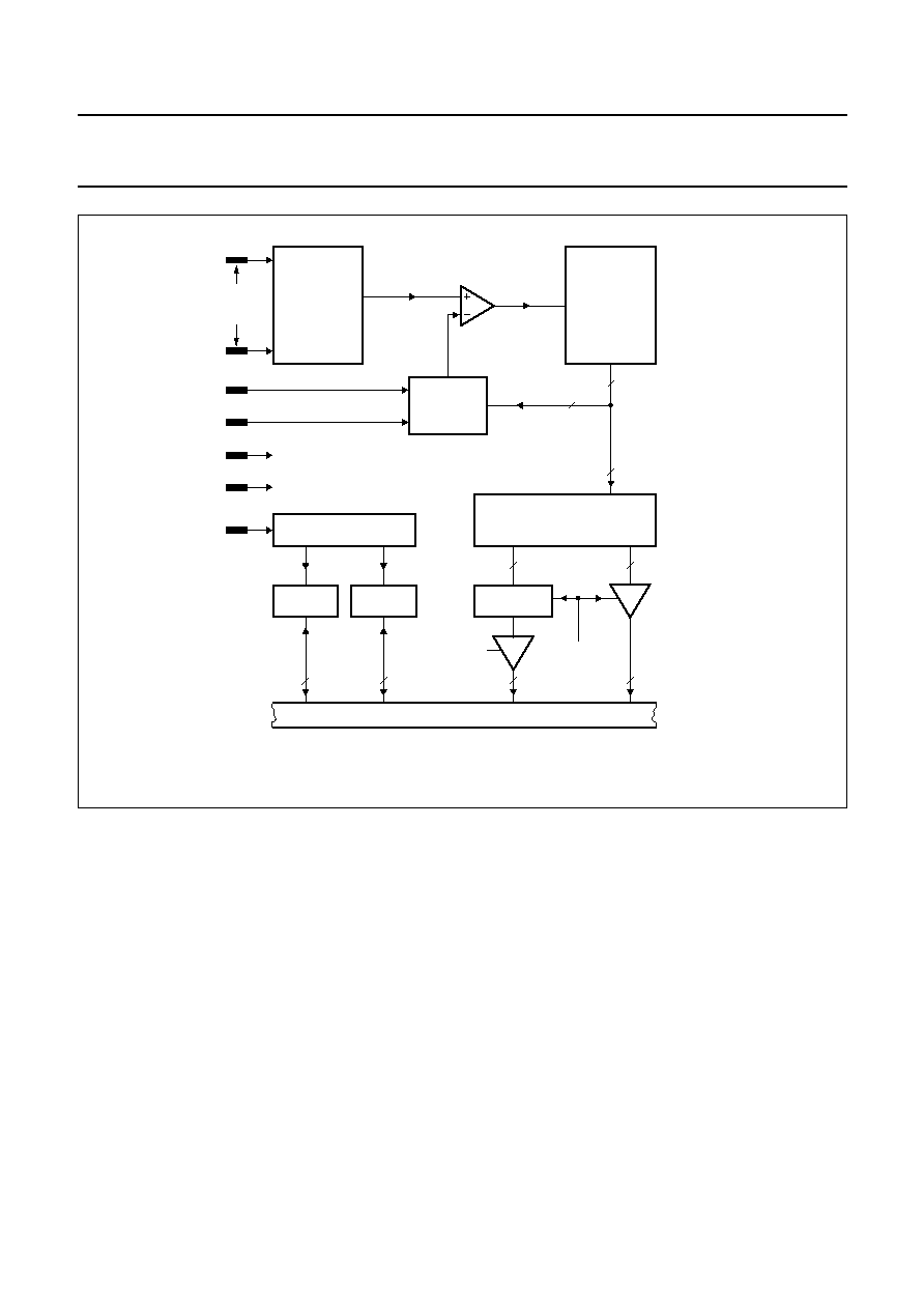
4
BLOCK DIAGRAM
handbook, full pagewidth
MHI023
RD
WR
PSEN
XTAL2
ALE
SELXTAL
RSTIN
XTAL1
AD0 to AD7
A8 to A15
EA
XTAL3
XTAL4
ADEXS
ADC0 to ADC7
V
ref(p)(A)
V
ref(n)(A)
RSTOUT
EW
CMSR0 to CMSR5
CMT0, CMT1
RT2
T2
CT0I to CT3I
P4
P5
RXD
TXD
P3
P2
P1
P0
T0
T1
INT0
INT1
V
DD
V
SS
V
DDA
V
SSA
THREE
16-BIT
COMPARATORS
WITH
REGISTERS
PARALLEL
I/O PORTS
&
EXT. BUS
SERIAL
UART
PORT
8-BIT
I/O
PORTS
FOUR
16-BIT
CAPTURE
LATCHES
16-BIT
TIMER/
EVENT
COUNTER
(T2)
16
16
COMPARATOR
OUTPUT
SELECTION
WATCHDOG
TIMER
(T3)
TWO 16 - BIT
TIMER/
EVENT
COUNTERS
(T0,T1)
80C51
core
excluding
ROM/RAM
CPU
PROGRAM
MEMORY
DATA MEMORY
256 bytes
RAM
+
1792 bytes
AUX-RAM
DUAL
PWM
PLL
OSCILLATOR
+
'SECONDS'
TIMER
I
2
C-BUS
SERIAL
I/O
ADC
8-bit internal bus
P8xC557E8
SDA
SCL
64 kbytes
ROM/
EPROM
PWM0
PWM1
(4)
(4)
(4)
(4)
(7)
(6)
(5)
(2)
(2)
(4)
(4)
(3)
(1)
(4)
(4)
Fig.1 Block diagram P8xC557E8.
(1)
Alternative function of Port
0.
(2)
Alternative function of Port
1.
(3)
Alternative function of Port
2.
(4)
Alternative function of Port
3.
(5)
Alternative function of Port
5.
(6)
Alternative function of Port
6.
(7)
Not present in P80C557E8.

1999 Mar 12
6
Philips Semiconductors
Product specification
8-bit microcontroller
P8xC557E8
5
FUNCTIONAL DIAGRAM
Fig.2 Functional diagram.
(1) Only the P87C557E8 with an alternative function.
(2) V
DDA
/V
SSA
- 2 analog supply pairs;
V
DD
/V
SS
- 4 digital supply pairs.
handbook, full pagewidth
MHI024
P8xC557E8
0
1
2
3
4
5
6
7
PORT 0
XTAL3
VDDA
VDD
VSSA
VSS
0
1
2
3
4
5
6
7
PORT 1
0
1
2
3
4
5
6
7
(2)
PORT 3
AD0
AD1
AD2
AD3
AD4
AD5
AD6
AD7
LOW ORDER
ADDRESS
AND
DATA BUS
alternative function
0
1
2
3
4
5
6
7
PORT 2
A8
A9
A10
A11
A12
A13
A14
A15
HIGH ORDER
ADDRESS
BUS
CT0I/INT2
CT1I/INT3
CT2I/INT4
CT3I/INT5
T2
RT2
0
1
2
3
4
5
6
7
PORT 5
0
1
2
3
4
5
6
7
PORT 4
RSTIN
RSTOUT
EW
alternative function
ADC0
CMSR0
ADC1
ADC2
ADC3
ADC4
ADC5
ADC6
ADC7
CMSR1
CMSR2
CMSR3
CMSR4
CMSR5
CMT0
CMT1
Vref(p)(A)
Vref(n)(A)
STADC
PSEN
PWM0
PWM1
XTAL1
XTAL2
RXD/DATA
TXD/CLOCK
T0
T1
RD
WR
INT1
INT0
ALE/PROG
(1)
EA/VPP
(1)
ADEXS
SCL
SDA
XTAL4
SELXTAL1

1999 Mar 12
7
Philips Semiconductors
Product specification
8-bit microcontroller
P8xC557E8
6
PINNING INFORMATION
6.1
Pinning diagram
Fig.3 Pin configuration QFP80/SOT318 version.
(1) Only the P87C557E8 with this alternative function.
handbook, full pagewidth
1
2
3
4
5
6
7
8
9
10
11
12
13
14
15
16
17
18
19
20
21
22
23
24
64
63
62
60
59
58
57
56
55
54
53
52
51
50
49
48
47
46
45
44
43
42
41
61
25
26
27
29
30
31
32
33
34
35
36
37
38
39
40
28
80
79
78
76
75
74
73
72
71
70
69
68
67
66
65
77
P8xC557E8
VSSA1
VDDA1
P5.7/ADC7
P5.6/ADC6
P5.5/ADC5
P5.4/ADC4
P5.3/ADC3
P5.2/ADC2
P5.1/ADC1
P5.0/ADC0
VSS1
VDD1
ADEXS
P4.0/CMSR0
P4.1/CMSR1
P4.2/CMSR2
P4.3/CMSR3
RSTOUT
P4.4/CMSR4
EW
PWM1
PWM0
Vref(p)(A)
Vref(n)(A)
P2.7/A15
P2.6/A14
P2.5/A13
P2.4/A12
P2.3/A11
P2.2/A10
P2.1/A9
P2.0/A8
VSS3
VDD3
V
SS4
V
DD4
V
SSA2
V
DDA2
XTAL1
XTAL2
n.c.
n.c.
P3.5/T1
P3.4/T0
P3.1/TXD
P3.0/RXD
P3.2/INT0
P3.3/INT1
P3.6/WR
P3.7/RD
PSEN
P4.5/CMSR5
P4.6/CMT0
P4.7/CMT1
V
DD2
V
SS2
RSTIN
P1.7
P1.6
SCL
SDA
P1.0/CT0I/INT2
P1.1/CT1I/INT3
P1.2/CT2I/INT4
P1.3/CT3I/INT5
P1.4/T2
P1.5/RT2
MHI025
P0.7/AD7
P0.6/AD6
P0.5/AD5
P0.4/AD4
P0.3/AD3
P0.2/AD2
P0.1/AD1
P0.0/AD0
XTAL3
XTAL4
SELXTAL1
EA/V
PP
(1)
ALE/PROG
(1)

1999 Mar 12
8
Philips Semiconductors
Product specification
8-bit microcontroller
P8xC557E8
6.2
Pin description
Table 1
Pin description for QFP80 (SOT318-2)
To avoid a `latch-up' effect at power-on: V
SS
-
0.5 V < `voltage at any pin at any time' < V
DD
+ 0.5 V.
SYMBOL
PIN
DESCRIPTION
V
ref(n)(A)
1
Low-end of ADC reference resistor.
V
ref(p)(A)
2
High-end of ADC reference resistor.
V
SSA1
3
Ground, analog part. For ADC receiver and reference voltage.
V
DDA1
4
Power supply, analog part (+5 V). For ADC receiver and reference voltage.
P5.7/ADC7 to
P5.0/ADC0
5 to 12
Port 5 (P5.7 to P5.0): 8-bit input port lines;
ADC7 to ADC0: 8 input channels to the ADC.
V
SS1
to V
SS4
13, 29,
54, 67
Ground; digital part; circuit ground potential. V
SS1
, V
SS2
, V
SS4
must be connected,
V
SS3
is internally connected to digital ground, but should be connected externally.
V
DD1
to V
DD4
14, 28,
53, 66
Power supply, digital part (+5 V). Power supply pins during normal operation and
power reduction modes. All pins must be connected.
ADEXS
15
Start ADC operation. Input starting ADC, triggered by a programmable edge; ADC
operation can also be started by software. This pin must not float.
PWM0
16
Pulse Width Modulation output 0.
PWM1
17
Pulse Width Modulation output 1.
EW
18
Enable Watchdog Timer (WDT): enable for T3 Watchdog Timer and disable
Power-down mode. This pin must not float.
P4.0/CMSR0 to
P4.5/CMSR5
19 to 22,
24, 25
Port 4 (P4.0 to P4.7): 8-bit quasi-bidirectional I/O port lines;
CMSR0 to CMSR5: compare and set/reset outputs for Timer T2;
CMT0 to CMT1: compare and toggle outputs for Timer T2.
P4.6/CMT0 to
P4.7/CMT1
26, 27
RSTOUT
23
Reset output of the P8xC557E8 for resetting peripheral devices during initialization
and Watchdog Timer overflow.
RSTIN
30
Reset input to reset the P8xC557E8.
P1.0/CT0I/INT2 to
P1.3/CT3I/INT5
31 to 34
Port 1 (P1.0 to P1.7): 8-bit quasi-bidirectional I/O port lines;
CT0I to CT3I: Capture timer inputs for Timer T2;
INT2 to INT5: external interrupts 2 to 5;
T2: T2 event input (rising edge triggered);
RT2: T2 timer reset input (rising edge triggered).
P1.4/T2 to
P1.5/RT2
35, 36
P1.6 to P1.7
37 to 38
SCL
39
I
2
C-bus serial clock I/O port. If SCL is not used, it must be connected to V
SS
.
SDA
40
I
2
C-bus serial data I/O port. If SDA is not used, it must be connected to V
SS
.
P3.0/RXD
41
Port 3 (P3.0 to P3.7): 8-bit quasi-bidirectional I/O port lines;
RXD: Serial input port;
TXD: Serial output port;
INT0: External interrupt input 0;
INT1: External interrupt input 1;
T0: Timer 0 external interrupt input;
T1: Timer 1external interrupt input;
WR: External Data Memory Write strobe;
RD: External Data Memory Read strobe.
P3.1/TXD
42
P3.2/INT0
43
P3.3/INT1
44
P3.4/T0
45
P3.5/T1
46
P3.6/WR
47
P3.7/RD
48
n.c.
49, 50
Not connected pins.
1999 Mar 12
9
Philips Semiconductors
Product specification
8-bit microcontroller
P8xC557E8
XTAL2
51
Crystal pin 2: output of the inverting amplifier that forms the oscillator.
Left open-circuit when an external oscillator clock is used.
XTAL1
52
Crystal pin 1: input to the inverting amplifier that forms the oscillator, and input to the
internal clock generator. Receives the external oscillator clock signal when an external
oscillator is used. Must be connected to logic HIGH if the PLL oscillator is selected
(SELXTAL1 = LOW).
P2.0/A08 to
P2.7/A15
55 to 62
Port 2 (P2.0 to P2.7): 8-bit quasi-bidirectional I/O port lines;
A08 to A15: High-order address byte for external memory.
PSEN
63
Program Store Enable output: read strobe to the external Program Memory via
Ports 0 and 2. Is activated twice each machine cycle during fetches from external
Program Memory. When executing out of external Program Memory two activations of
PSEN are skipped during each access to external Data Memory. PSEN is not
activated (remains HIGH) during no fetches from external Program Memory. PSEN
can sink/source 8 LSTTL inputs. It can drive CMOS inputs without external pull-ups.
ALE/PROG
64
Address Latch Enable output. Latches the low byte of the address during access of
external memory in normal operation. It is activated every six oscillator periods except
during an external Data Memory access. ALE can sink/source 8 LSTTL inputs. It can
drive CMOS inputs without an external pull-up. To prohibit the toggling of ALE pin (RFI
noise reduction) the bit RFI (SFR: PCON.5) must be set by software; see Section 2.2.
PROG: the programming pulse input; alternative function for the P87C557E8.
EA/V
PP
65
External Access input. If, during reset, EA is held at a TTL level HIGH the CPU
executes out of the internal Program Memory. If, during reset, EA is held at a TTL level
LOW the CPU executes out of external Program Memory via Port 0 and Port 2. EA is
not allowed to float. EA is latched during reset and don't care after reset.
V
PP
: the programming supply voltage; alternative function for the P87C557E8.
P0.7/AD7 to
P0.0/AD0
68 to 75
Port 0 (P0.7 to P0.0): 8-bit open-drain bidirectional I/O port lines;
AD7 to AD0: Multiplexed Low-order address and Data bus for external memory.
V
DDA2
76
Power supply, analog part (+5 V). For PLL oscillator.
V
SSA2
77
Ground, analog part. For PLL oscillator.
XTAL3
78
Crystal pin 3: output of the inverting amplifier that forms the 32 kHz oscillator.
XTAL4
79
Crystal pin 2: input to the inverting amplifier that forms the 32 kHz oscillator. XTAL3 is
pulled LOW if the PLL oscillator is not selected (SELXTAL1 = 1) or if reset is active.
SELXTAL1
80
SELXTAL1 = HIGH, selects the HF oscillator, using the XTAL1/XTAL2 crystal.
If SELXTAL1 = LOW the PLL is selected for clocking of the controller, using the
XTAL3/XTAL4 crystal.
SYMBOL
PIN
DESCRIPTION

1999 Mar 12
10
Philips Semiconductors
Product specification
8-bit microcontroller
P8xC557E8
7
FUNCTIONAL DESCRIPTION
The P8xC557E8 is a stand-alone high-performance
microcontroller designed for use in real time applications
such as instrumentation, industrial control, medium to
high-end consumer applications and specific automotive
control applications.
In addition to the 80C51 standard functions, the device
provides a number of dedicated hardware functions for
these applications.
The P8xC557E8 is a control-oriented CPU with on-chip
program and Data Memory, but it cannot be extended with
external Program Memory. It can access up to 64 kbytes
of external Data Memory. For systems requiring extra
capability, the P8xC557E8 can be expanded using
standard memories and peripherals.
The functional description of the device is described in:
Chapter 8 "Memory organization"
Chapter 9 "I/O facilities"
Chapter 10 "Pulse Width Modulated outputs"
Chapter 11 "Analog-to-Digital Converter (ADC)"
Chapter 12 "Timers/counters"
Chapter 13 "Serial I/O ports"
Chapter 14 "Interrupt system"
Chapter 15 "Reduced power modes"
Chapter 16 "Oscillator circuits"
Chapter 17 "Reset circuitry".

1999 Mar 12
11
Philips Semiconductors
Product specification
8-bit microcontroller
P8xC557E8
8
MEMORY ORGANIZATION
The Central Processing Unit (CPU) manipulates operands
in three memory spaces; these are the 64 kbytes external
Data Memory, 2048 bytes internal Data Memory
(consisting of 256 bytes standard RAM and 1792 bytes
AUX-RAM) and the 64 kbytes internal or 64 kbytes
external Program Memory (see Fig.4).
8.1
Program Memory
The Program Memory of the P8xC557E8 consists of
64 kbytes ROM or 64 kbytes EPROM. If, during reset, the
EA pin was held HIGH, the P8xC557E8 always executes
out of the internal Program Memory. If the EA pin was held
LOW during reset the P8xC557E8 fetches all instructions
from the external Program Memory. The EA input is
latched during reset and is don't care after reset.
The internal Program Memory content is protected by
setting a mask programmable security bit (ROM) or by the
software programmable security bits (EPROM)
respectively, i.e. it cannot be read out at any time by any
test mode or by any instruction in the external Program
Memory space. The MOVC instructions are the only ones
which have access to program code in the internal or
external Program Memory. The EA input is latched during
reset and is don't care after reset. This implementation
prevents from reading internal program code by switching
from external Program Memory to internal Program
Memory during MOVC instruction or an instruction that
handles immediate data. Table 2 lists the access to the
internal and external Program Memory with MOVC
instructions whether the security feature has been
activated or not.
Due to the maximum size of the internal Program Memory,
the MOVC instructions can always operate either in the
internal or in the external Program Memory.
Table 2
Memory access by the MOVC instruction
For code protection of the P87C557E8 see Section 23.2.
Note
1. Not applicable due to 64 kbytes internal Program
Memory.
MOVC
INSTRUCTION
PROGRAM MEMORY ACCESS
INTERNAL
EXTERNAL
MOVC in internal
Program Memory
YES
NO
(1)
MOVC in external
Program Memory
NO
(1)
YES
8.2
Internal Data Memory
The internal Data Memory is divided into three physically
separated parts: 256 bytes of RAM, 1792 bytes of
AUX-RAM, and a 128 bytes Special Function Registers
(SFRs) area. These parts can be addressed each in a
different way as described in Sections 8.2.1 to 8.2.2 and
Table 3.
Table 3
Internal Data Memory map
8.2.1
RAM
∑
RAM 0 to 127 can be addressed directly and indirectly
as in the 80C51. Address pointers are R0 and R1 of the
selected register bank.
∑
RAM 128 to 255 can only be addressed indirectly.
Address pointers are R0 and R1 of the selected register
bank.
Four register banks, each 8 registers wide, occupy
locations 0 through 31 in the lower RAM area. Only one of
these banks may be enabled at a time. The next 16 bytes,
locations 32 through 47, contain 128 directly addressable
bit locations. The stack can be located anywhere in the
internal 256 bytes RAM. The stack depth is only limited by
the available internal RAM space of 256 bytes (see Fig.6).
All registers except the Program Counter and the four
register banks reside in the Special Function Register
address space.
8.2.2
S
PECIAL
F
UNCTION
R
EGISTERS
The Special Function Registers can only be addressed
directly in the address range from 128 to 255 (see Fig.7).
8.2.3
AUX-RAM
∑
AUX-RAM 0 to 1791 is indirectly addressable via page
register (XRAMP) and MOVX-Ri instructions, unless it is
disabled by setting ARD = 1 (see Fig.5). When
executing from internal Program Memory, an access to
AUX-RAM 0 to 1791 will not affect the ports P0, P2,
P3.6 and P3.7.
∑
AUX-RAM 0 to 1791 is also indirectly addressable as
external Data Memory locations 0 to 1791 via MOVX-Ri
instructions, unless it is disabled by setting ARD = 1.
MEMORY
LOCATION
ADDRESS MODE
RAM
0 to 127
Direct and indirect
128 to 255
Indirect only
SFR
128 to 255
Direct only
AUX-RAM
0 to 1791
Indirect only with MOVX

1999 Mar 12
12
Philips Semiconductors
Product specification
8-bit microcontroller
P8xC557E8
An access to external Data Memory locations higher than
1791 will be performed with the MOVX @DPTR
instructions in the same way as in the 80C51 structure, so
with P0 and P2 as data/address bus and P3.6 and P3.7 as
write and read timing signals.
Note that the external Data Memory cannot be accessed
with R0 and R1 as address pointer if the AUX-RAM is
enabled (ARD = 0, default).
8.2.4
AUX-RAM P
AGE
R
EGISTER
(XRAMP)
The AUX-RAM Page Register is used to select one of
seven 256-bytes pages of the internal 1792 bytes
AUX-RAM for MOVX-accesses via R0 or R1. Its reset
value is `XXXX X000B'.
Table 4
AUX-RAM Page Register (address FAH)
Table 5
Description of XRAMP bits
Table 6
Memory locations for all possible MOVX-accesses
X = don't care.
Note
1. ARD: AUX-RAM disable, is a bit in SFR PCON (bit PCON.6); see Section 15.5.
7
6
5
4
3
2
1
0
XRAMPx
XRAMPx
XRAMPx
XRAMPx
XRAMPx
XRAMP2
XRAMP1
XRAMP0
BIT
SYMBOL
FUNCTION
7 to 3
XRAMPx
Reserved for future use. During read XRAMPx = undefined; a write
operation must write logic 0s to these locations.
2 to 0
XRAMP2 to XRAMP0
AUX-RAM page select bits 2 to 0; see Table 6.
ARD
(1)
XRAMP2 XRAMP1 XRAMP0
MEMORY LOCATIONS
MOVX @Ri,A and MOVX A,@Ri instructions access
0
0
0
0
AUX-RAM locations 0 to 255 (reset condition)
0
0
0
1
AUX-RAM locations 256 to 511
0
0
1
0
AUX-RAM locations 512 to 767
0
0
1
1
AUX-RAM locations 768 to 1023
0
1
0
0
AUX-RAM locations 1024 to 1279
0
1
0
1
AUX-RAM locations 1280 to 1535
0
1
1
0
AUX-RAM locations 1536 to 1791
0
1
1
1
No valid memory access; reserved for future use
1
X
X
X
External RAM locations 0 to 255
MOVX @DPTR,A and MOVX A,@DPTR instructions access
0
X
X
X
AUX-RAM locations 0 to 1791 (reset condition);
External RAM locations 1792 to 65535
1
X
X
X
External RAM locations 0 to 65535

1999 Mar 12
13
Philips Semiconductors
Product specification
8-bit microcontroller
P8xC557E8
Fig.4 Memory map and address space.
handbook, full pagewidth
MBH077
INTERNAL
(EA = 1)
64 kbytes
EXTERNAL
(EA = 0)
64 kbytes
64 kbytes
0
0
0
127
255
INDIRECT ONLY
OVERLAPPED SPACE
SPECIAL
FUNCTION
REGISTERS
AUXILIARY
RAM
(ARD = 0)
1792 bytes
EXTERNAL DATA
MEMORY
INTERNAL DATA
MEMORY
PROGRAM MEMORY
MAIN RAM
DIRECT AND
INDIRECT
1791
(ARD = 1)
Fig.5 Indirect addressing AUX-RAM (1792 bytes); ARD = 0 (bit PCON.6).
handbook, full pagewidth
MBH078
(XRAMP) = 06 H
0
255
255
1791
1536
1535
(XRAMP) = 05 H
0
255
1280
1279
(XRAMP) = 04 H
0
255
1024
1023
(XRAMP) = 03 H
0
255
768
767
(XRAMP) = 02 H
0
255
512
511
(XRAMP) = 01 H
0
255
0
256
255
0
(XRAMP) = 00 H
MOVX @DPTR, A
MOVX A, @DPTR
MOVX @Ri, A
MOVX A, @Ri

1999 Mar 12
14
Philips Semiconductors
Product specification
8-bit microcontroller
P8xC557E8
8.3
Addressing
The P8xC557E8 has five methods for addressing:
∑
Register
∑
Direct
∑
Register-Indirect
∑
Immediate
∑
Base-Register plus Index-Register-Indirect.
The first three methods can be used for addressing
destination operands. Most instructions have a
`destination/source' field that specifies the data type,
addressing methods and operands involved.
For operations other than MOVs, the destination operand
is also a source operand.
Access to memory addresses is as follows:
∑
Register in one of the four register banks through
Register, Direct or Register-Indirect addressing.
∑
Internal RAM (2048 bytes) through Direct or
Register-Indirect addressing.
≠ Internal RAM: bytes 0 to 127; may be addressed
directly/indirectly.
≠ Internal RAM: bytes 128 to 255; share their address
location with the SFRs and so may only be addressed
indirectly as data RAM.
≠ AUX-RAM: bytes 0 to 1791; can only be addressed
indirectly via MOVX.
∑
Special Function Registers through direct addressing at
address locations 128 to 255 (see Fig.7).
∑
External Data Memory through Register-Indirect
addressing.
∑
Program Memory look-up tables through Base-Register
plus Index-Register-Indirect addressing.
Fig.6 Internal MAIN RAM bit addresses.
MBH079
7F
7E
7D
7C
7B
7A
79
78
77
76
75
74
73
72
71
70
6F
6E
6D
6C
6B
6A
69
68
67
66
65
64
63
62
61
60
5F
5E
5D
5C
5B
5A
59
58
57
56
55
54
53
52
51
50
4F
4E
4D
4C
4B
4A
49
48
47
46
45
44
43
42
41
40
3F
3E
3D
3C
3B
3A
39
38
37
36
35
34
33
32
31
30
2F
2E
2D
2C
2B
2A
29
28
27
26
25
24
23
22
21
20
1F
1E
1D
1C
1B
1A
19
18
17
16
15
14
13
12
11
10
0F
0E
0D
0C
0B
0A
09
08
07
06
05
04
03
02
01
00
18H
17H
10H
0FH
08H
07H
00H
24
23
31
16
15
8
7
0
BANK 0
BANK 1
BANK 2
BANK 3
32
33
34
35
36
37
38
39
40
41
42
43
44
45
46
47
(MSB)
(LSB)
255
FFH
2FH
2EH
2DH
2CH
2BH
2AH
29H
28H
27H
26H
25H
24H
23H
22H
21H
20H
1FH
BYTE
ADDRESS
(DECIMAL)
BYTE
ADDRESS
(HEX)
BIT ADDRESS
(HEX)

1999 Mar 12
15
Philips Semiconductors
Product specification
8-bit microcontroller
P8xC557E8
Fig.7 Special Function Registers bit addresses.
handbook, full pagewidth
MBH456
FF
(MSB)
(LSB)
IP1
FFH
F8H
REGISTER
(MNEMONIC)
BYTE ADDRESS
(HEX)
BIT ADDRESS
(HEX)
PT2
PCM2
PCM1
PCM0
PCT3
PCT2
PCT1
PCT0
FE
FD
FC
FB
FA
F9
F8
F7
B
F0H
F6
F5
F4
F3
F2
F1
F0
ET2
ECM2
ECM1
ECM0
ECT3
ECT2
ECT1
ECT0
EF
IEN1
F8H
EE
ED
EC
EB
EA
E9
E8
C7
P4
C0H
C6
C5
C4
C3
C2
C1
C0
-
PAD
PS1
PS0
PT1
PX1
PT0
PX0
BF
IP0
B8H
BE
BD
BC
BB
BA
B9
B8
B7
P3
B0H
B6
B5
B4
B3
B2
B1
B0
EA
EAD
ES1
ES0
ET1
EX1
ET0
EX0
AF
IEN0
A8H
AE
AD
AC
AB
AA
A9
A8
A7
P2
A0H
A6
A5
A4
A3
A2
A1
A0
SM0
SM1
SM2
REN
TB8
RB8
TI
RI
9F
S0CON
98H
9E
9D
9C
9B
9A
99
98
97
P1
90H
96
95
94
93
92
91
90
TF1
TR1
TF0
TR0
IE1
IT1
IE0
IT0
8F
TCON
88H
8E
8D
8C
8B
8A
89
88
87
P0
80H
86
85
84
83
82
81
80
E7
ACC
E0H
E6
E5
E4
E3
E2
E1
E0
CR2
ENS1
STA
STO
SI
AA
CR1
CR0
CY
AC
F0
RS1
RS0
OV
F1
P
DF
S1CON
D8H
PSW
D0H
TM2IR
C8H
DE
DD
DC
DB
DA
D9
D8
D7
D6
D5
D4
D3
D2
D1
D0
T2OV
CMI2
CMI1
CMI0
CTI3
CTI2
CTI1
CTI0
CF
CE
CD
CC
CB
CA
C9
C8

1999 Mar 12
16
Philips Semiconductors
Product specification
8-bit microcontroller
P8xC557E8
9
I/O FACILITIES
The P8xC557E8 has six 8-bit ports. Ports 0 to 3 are the
same as in the 80C51, with the exception of the additional
functions of Port 1. The parallel I/O function of Port 4 is
equal to that of Ports 1, 2 and 3. All ports are bidirectional
with the exception of Port 5 which is only a parallel input
port.
Ports 0, 1, 2, 3, 4 and 5 perform the following alternative
functions:
Port 0 Provides the multiplexed low-order address and
data bus used for expanding the P8xC557E8 with
standard memories and peripherals.
Port 1 Is used for a number of special functions:
∑
4 capture inputs (or external interrupt request
inputs if capture information is not utilized)
∑
external counter input
∑
external counter reset input.
Port 2 Provides the high-order address bus when the
P8xC557E8 is expanded with external Data
Memory and / or the P8xC557E8 executes from
external Program Memory.
Port 3 Pins can be configured individually to provide:
∑
External interrupt request inputs
∑
Counter inputs
∑
Receiver input and transmitter output of serial
port SIO 0 (UART)
∑
Control signals to read and write external Data
Memory.
Port 4 Can be configured to provide signals indicating a
match between timer/counter T2 and its compare
registers.
Port 5 May be used in conjunction with the ADC interface.
Unused analog inputs can be used as digital inputs.
As Port 5 lines may be used as inputs to the ADC,
these digital inputs have an inherent hysteresis to
prevent the input logic from drawing too much
current from the power lines when driven by analog
signals. Channel-to-channel crosstalk should be
taken into consideration when both digital and
analog signals are simultaneously input to Port 5
(see Chapter 21).
A pin of which the alternative function is not used may be
used as normal bidirectional I/O. The generation or use of
a Port 1, Port 3 or Port 4 pin as an alternative function is
carried out automatically by the P8xC557E8 provided the
associated Special Function Register bit is set HIGH.
The SDA and SCL lines serve the serial port SI01
(I
2
C-bus). Because the I
2
C-bus may be active while the
device is disconnected from V
DD
, these pins are provided
with open-drain drivers.
Figure 8 shows the pull-up arrangements of Ports 1 to 4;
Transistor `p1' is turned on for 2 oscillator periods after Q
makes a HIGH-to-LOW transition. During this time, `p1'
also turns on `p3' through the inverter to form an additional
pull-up.
Fig.8 I/O buffers in the P8xC557E8 (Port 1 to Port 4).
handbook, full pagewidth
MLC926 - 1
p1
p2
p3
input data
read port pin
2 oscillator
periods
n
strong pull-up
I/O PIN
V
I1
Q
from port latch
INPUT
BUFFER
DD

1999 Mar 12
17
Philips Semiconductors
Product specification
8-bit microcontroller
P8xC557E8
10 PULSE WIDTH MODULATED OUTPUTS
The P8xC557E8 contains two Pulse Width Modulated
(PWM) output channels (see Fig.9). These channels
generate pulses of programmable length and interval.
The repetition frequency is defined by an 8-bit prescaler
PWMP, which supplies the clock for the counter.
The prescaler and counter are common to both PWM
channels. The 8-bit counter counts modulo 255, i.e., from
0 to 254 inclusive. The value of the 8-bit counter is
compared to the contents of two registers: PWM0 and
PWM1.
Provided the contents of either of these registers is greater
than the counter value, the corresponding PWM0 or
PWM1 output is set LOW. If the contents of these registers
are equal to, or less than the counter value, the output will
be HIGH. The pulse-width-ratio is therefore defined by the
contents of the registers PWM0 and PWM1.
The pulse-width-ratio is in the range of
0
/
255
to
255
/
255
and
may be programmed in increments of
1
/
255
.
Buffered PWM outputs may be used to drive DC motors.
The rotation speed of the motor would be proportional to
the contents of PWMn. The PWM outputs may also be
configured as a dual DAC.
In this application, the PWM outputs must be integrated
using conventional operational amplifier circuitry. If the
resulting output voltages have to be accurate, external
buffers with their own analog supply should be used to
buffer the PWM outputs before they are integrated.
The repetition frequency f
PWM
, at the PWMn outputs is
given by:
This gives a repetition frequency range of 123 Hz to
31.4 kHz (at f
clk
= 16 MHz). By loading the PWM registers
with either 00H or FFH, the PWM channels will output a
constant HIGH or LOW level, respectively. Since the 8-bit
counter counts modulo 255, it can never actually reach the
value of the PWM registers when they are loaded with
FFH.
When a compare register (PWM0 or PWM1) is loaded with
a new value, the associated output is updated
immediately. It does not have to wait until the end of the
current counter period. Both PWMn output pins are driven
by push-pull drivers. These pins are not used for any other
purpose.
f
PWM
f
CLK
2
PWMP
1
+
(
)
◊
255
◊
---------------------------------------------------------------
=
Fig.9 Functional diagram of Pulse Width Modulated outputs.
handbook, full pagewidth
MGA154
I
N
T
E
R
N
A
L
B
U
S
fclk
PWMP
PWM1
PRESCALER
8-BIT COUNTER
1/2
PWM0
8-BIT COMPARATOR
8-BIT COMPARATOR
OUTPUT
BUFFER
PWM1
OUTPUT
BUFFER
PWM0
1999 Mar 12
18
Philips Semiconductors
Product specification
8-bit microcontroller
P8xC557E8
10.1
Prescaler Frequency Control Register (PWMP)
Reading PWMP gives the current reload value. The actual count of the prescaler cannot be read.
Table 7
Prescaler Frequency Control Register (address FEH)
Table 8
Description of PWMP bits
10.2
Pulse Width Register 0 (PWM0)
Table 9
Pulse width register (address FCH)
Table 10 Description of PWM0 bits
10.3
Pulse Width Register 1 (PWM1)
Table 11 Pulse width register (address FDH)
Table 12 Description of PWM1 bits
7
6
5
4
3
2
1
0
PWMP.7
PWMP.6
PWMP.5
PWMP.4
PWMP.3
PWMP.2
PWMP.1
PWMP.0
BIT
SYMBOL
DESCRIPTION
7 to 0
PWMP.7 to PWMP.0
Prescaler division factor. The Prescaler division factor = (PWMP) + 1.
7
6
5
4
3
2
1
0
PWM0.7
PWM0.6
PWM0.5
PWM0.4
PWM0.3
PWM0.2
PWM0.1
PWM0.0
BIT
SYMBOL
DESCRIPTION
7 to 0
PWM0.7 to PWM0.0
Pulse width ratio.
7
6
5
4
3
2
1
0
PWM1.7
PWM1.6
PWM1.5
PWM1.4
PWM1.3
PWM1.2
PWM1.1
PWM1.0
BIT
SYMBOL
DESCRIPTION
7 to 0
PWM1.7 to PWM1.0
Pulse width ratio.
LOW/HIGH ratio of PWM0 signals
PWM0
(
)
255
PWM0
(
)
≠
------------------------------------------
=
LOW/HIGH ratio of PWM1 signals
PWM1
(
)
255
PWM1
(
)
≠
------------------------------------------
=

1999 Mar 12
19
Philips Semiconductors
Product specification
8-bit microcontroller
P8xC557E8
11 ANALOG-TO-DIGITAL CONVERTER (ADC)
11.1
ADC features
∑
10-bit resolution
∑
8 multiplexed analog inputs
∑
Programmable autoscan of the analog inputs
∑
Bit oriented 8-bit scan-select register to select analog
inputs
∑
Continuous scan or one time scan configurable from
1 to 8 analog inputs
∑
Start of a conversion by software or with an external
signal
∑
Eight 10-bit buffer registers, one register for each analog
input channel
∑
Interrupt request after one channel scan loop
∑
Programmable prescaler (dividing by 2, 4, 6, 8) to adapt
to different system clock frequencies
∑
Conversion time for one analog-to-digital conversion:
15 to 50
µ
s
∑
Differential non-linearity (DL
e
): ±
1 LSB
∑
Integral non-linearity (IL
e
):
±
2 LSB
∑
Offset error (OS
e
): ±
2 LSB
∑
Gain error (G
e
):
±
4%
∑
Absolute voltage error (A
e
): 3 LSB
∑
Channel-to-channel matching (M
ctc
):
±
1 LSB
∑
Crosstalk between analog inputs (C
t
): < 60 dB at
100 kHz
∑
Monotonic and no missing codes
∑
Separated analog (V
DDA
, V
SSA
) and digital (V
DD
, V
SS
)
supply voltages
∑
Reference voltage at two special pins: V
ref(n)(A)
and
V
ref(p)(A)
.
For information on the ADC characteristics, refer to
Chapter 21.
11.2
ADC functional description
The P8xC557E8 has a 10-bit successive approximation
ADC with 8 multiplexed analog input channels, comprising
a high input impedance comparator, DAC (built with
1024 series resistors and analog switches), registers and
control logic. Input voltage range is from V
ref(n)(A)
(typical 0 V) to V
ref(p)(A)
(typical +5 V).
Each of the set of 8 buffer registers (10-bit wide) store the
conversion results of the proper analog input channel.
Eleven Special Function Registers (SFRs) perform the
user software interface to the ADC; see Table 14 for an
overview of the ADC SFRs. In order to have a minimum of
ADC service overhead in the microcontroller program, the
ADC is able to operate autonomously within its user
configurable autoscan function.
Figure 10 shows the functional diagram of the ADC.
11.3
ADC timing
A programmable prescaler is controlled by the user
selectable bits ADPR1 and ADPR0 in SFR ADCON to
adapt the conversion time for different microcontroller
clock frequencies.
Table 13 shows conversion times (t
ADC
) for one
analog-to-digital conversion at some convenient system
clock frequencies (f
clk
) and ADC programmable prescaler
divisors: m.
Conversion time t
ADC
= (6
◊
m + 1) machine cycles.
A conversion time t
ADC
consists of one sample time period
(which equals two bit conversion times), 10 bit conversion
time periods and one machine cycle to store the result.
After result storage an extra initializing time period follows
to select the next analog input channel (according to the
contents of SFR ADPSS), before the input signal is
sampled.Thus the time period between two adjacent
conversions within an autoscan loop is larger than the pure
time t
ADC
. This autoscan cycle time is (7
◊
m) machine
cycles.
At the start of an autoscan conversion the time between
writing to SFR ADCON and the first analog input signal
sampling depends on the current prescaler value (m) and
the relative time offset between this write operation and the
internal (divided) ADC clock. This gives a variation range
for the analog-to-digital conversion start time of (
1
/
2
◊
m)
machine cycles.
Table 13 Conversion time configuration examples
Note
1. Prohibited t
ADC
values; for t
ADC
outside the limits of
15
µ
s
t
ADC
50
µ
s, the specified ADC
characteristics are not guaranteed.
m
t
ADC
(
µ
s) at f
CLK
:
6 MHz
8 MHz
12 MHz
16 MHz
2
26.00
19.50
13.00
(1)
9.75
(1)
4
50.00
37.50
25.00
18.75
6
74.00
(1)
55.50
(1)
37.00
27.75
8
98.00
(1)
73.50
(1)
49.00
36.75
1999 Mar 12
20
Philips Semiconductors
Product specification
8-bit microcontroller
P8xC557E8
Fig.10 Functional diagram of ADC.
handbook, full pagewidth
MBH080
8
8
2
2
10
10
10
8
2 LATCHES
ADCON
SCAN LOGIC
ANALOG
MULTIPLEXER
INTERNAL BUS
8
ADPSS
Read ADRSLn
Read ADRSH
8 x 10-BIT RESULT
REGISTERS
ADEXS
VSSA1
VDDA1
Vref(n)(A)
Vref(p)(A)
ADC0
to
ADC7
SAR
DAC
COMPARATOR
11.4
ADC configuration and operation
Every analog-to-digital conversion is an autoscan
conversion. The two user selectable general operation
modes are continuous scan and one-time scan mode.
The desired analog input port channel(s) for conversion
is(are) selected by programming analog-to-digital input
port scan-select bits in SFR ADPSS. An analog input
channel is included in the autoscan loop if the
corresponding bit in SFR ADPSS is logic 1, a channel is
skipped if the corresponding bit in SFR ADPSS is logic 0.
An autoscan is always started according to the lowest bit
position of SFR ADPSS that contains a logic 1.
An autoscan conversion is started by setting the flag
ADSST in register ADCON either by software or by an
external start signal at input pin ADEXS, if enabled.
Either no edge (external start totally disabled), a rising
edge or/and a falling edge of ADEXS is selectable for
external conversion start by the bits ADSRE and ADSFE
in register ADCON.
After completion of an analog-to-digital conversion the
10-bit result is stored in the corresponding 10-bit buffer
register. Then the next analog input is selected according
to the next higher set bit position in ADPSS, converted and
stored, and so on.
When the result of the last conversion of this autoscan loop
is stored, the ADC interrupt flag ADINT (SFR ADCON), is
set. It is not cleared by interrupt hardware - it must be
cleared by software.

1999 Mar 12
21
Philips Semiconductors
Product specification
8-bit microcontroller
P8xC557E8
In continuous scan mode (ADCSA = 1; ADCON.2) the
ADC start and status flag ADSST (ADCON.3) retains the
set state and the autoscan loop restarts from the
beginning. In one-time scan mode (ADCSA = 0)
conversions stop after the last selected analog input was
converted, ADINT (ADCON.4) is set and ADSST is
cleared automatically.
ADSST cannot be set (neither externally nor by software)
as long as ADINT = 1, i.e. as long as ADINT is set, a new
conversion start - by setting flag ADSST - is inhibited;
actually it is only delayed until ADINT is cleared. If a logic 1
is written to ADSST while ADINT = 1, this new value is
internally latched and preserved, not setting ADSST until
ADINT = 0. In this state, a read of SFR ADCON will display
ADSST = 0, because always the effective ADC status is
read.
Note that under software control the analog inputs can also
be converted in arbitrary order, when one-time scan mode
is selected and in SFR ADPSS only one bit is set at a time.
In this case ADINT is set and ADSST is cleared after every
conversion.
11.5
ADC during Idle and Power-down mode
The analog-to-digital converter is active only when the
microcontroller is in normal operating mode. If the Idle or
Power-down mode is activated, then the ADC is switched
off and put into a power saving idle state - a conversion in
progress is aborted, a previously set ADSST flag is cleared
and the internal clock is halted. The conversion result
registers are not affected.
The interrupt flag ADINT will not be set by activation of Idle
or Power-down mode. A previously set flag ADINT will not
be cleared by the hardware. (Note: ADINT cannot be
cleared by hardware at all, except for a reset - it must be
cleared by the user software.)
After a wake-up from Idle or Power-down mode a set flag
ADINT indicates that at least one autoscan loop was
finished completely before the microcontroller was put into
the respective power reduction mode and it indicates that
the stored result data may be fetched now - if desired.
For further information on Idle and Power-down modes,
refer to Chapter 15.
11.6
ADC resolution and characteristics
The ADC system has its own analog supply pins V
DDA1
and V
SSA1
. It is referenced by two special reference
voltage input pins sourcing the resistance ladder of the
DAC: V
ref(p)(A)
and V
ref(n)(A)
. The voltage between V
ref(p)(A)
and V
ref(n)(A)
defines the full-scale range. Due to the 10-bit
resolution the full scale range is divided into 1024 unit
steps.
The unit step voltage is 1 LSB, which is typically 5 mV
(V
ref(p)(A)
= 5.12 V, V
ref(n)(A)
= 0 V = V
SSA1
).
The DAC's resistance ladder has 1023 equally spaced
taps, separated by a unit resistance `R'.
The first tap is located 0.5
◊
R above V
ref(n)(A)
, the last tap
is located 1.5
◊
R below V
ref(p)(A)
. This results in a total
ladder resistance of 1024
◊
R. This structure ensures that
the DAC is monotonic and results in a symmetrical
quantization error. For input voltages between:
∑
V
ref(n)(A)
and [V
ref(n)(A)
+
1
/
2
◊
LSB] the 10-bit conversion
result code will be 0000000000B (= 000H or 0D)
∑
[V
ref(p)(A)
-
3
/
2
◊
LSB] and V
ref(p)(A)
the 10-bit conversion
result code will be 1111111111B (= 3FFH or 1023D).
The result code corresponding to an analog input voltage
(V
in(A)
) can be calculated from the formula:
The analog input voltage should be stable when it is
sampled for conversion. At any times the input voltage
slew rate must be less than 10 V/ms (5 V conversion
range) in order to prevent an undefined result.
This maximum input voltage slew rate can be ensured by
an RC low pass filter with R = 2.2 k
and C = 100 nF.
The capacitor between analog input pin and analog
ground pin shall be placed close to the pins in order to
have maximum effect in minimizing input noise coupling.
11.7
ADC after reset
After a reset of the microcontroller the ADCON and
ADPSS registers are initialized to zero. Registers ADRSLn
and ADRSH are not initialized by a reset.
Result code
1024
V
in(A)
V
ref(n)(A)
≠
V
ref(p)(A)
V
ref(n)(A)
≠
------------------------------------------------
◊
=

1999 Mar 12
22
Philips Semiconductors
Product specification
8-bit microcontroller
P8xC557E8
11.8
ADC Special Function Registers
Table 14 ADC Special Function Registers overview
The SFRs are not bit addressable. For more information on Special Function Registers refer to Section 8.2.
11.8.1
ADC R
ESULT
R
EGISTERS
The binary result code of the analog-to-digital conversions is accessed by the ADC Result Registers:
∑
ADRSLn (ADRSL0 to ADRSL7); eight input channel related conversion result SFRs for the 8 result lower bytes. Each
of ADRSLn is associated with the indexed analog input channel ADCn (ADC0/P5.0 to ADC7/P5.7).
∑
ADRSH for the ADC; one general SFR for the 2 result upper bits (bit 9 and 8).
During read (by software) of the ADRSLn register, simultaneously the two highest bits of the 10-bit conversion result are
copied into the two latches, ADRSH.0 and ADRSH.1 (SFR ADRSH) preserving them until the next read of any ADRSLn
register. Thus to ensure that the 10-bit result of the same single analog-to-digital conversion is captured, first read the
ADRSLn register and then the ADRSH register.
Table 15 ADC Result Register Low Byte; ADRSLn; n = 0 to 7 (address see 86H to F6H)
Table 16 Description of ADRSLn bits
ADDRESS
NAME
R/W
RESET
VALUE
DESCRIPTION
86H
ADRSL0
R
-
ADC Result Registers Low Byte: ADRSL0 to ADRSL7; The read value
after reset is indeterminate. Their data are not affected by chip reset.
96H
ADRSL1
A6H
ADRSL2
B6H
ADRSL3
C6H
ADRSL4
D6H
ADRSL5
E6H
ADRSL6
F6H
ADRSL7
F7H
ADRSH
R
00H
ADC Result Register High Bits: one common result SFR for the upper
2 result bits.
E7H
ADPSS
R/W
00H
ADC Input Port Scan-Select Register. Contains control bits to select the
analog input channel(s) to be scanned for analog-to-digital conversion.
D7H
ADCON
R/W
00H
ADC Control Register. Contains control and status bits for the
analog-to-digital converter peripheral block.
C7H
P5
R
-
Digital Input Port Register; shared with analog inputs. P5 is not affected by
chip reset.
7
6
5
4
3
2
1
0
ADRSn.7
ADRSn.6
ADRSn.5
ADRSn.4
ADRSn.3
ADRSn.2
ADRSn.1
ADRSn.0
BIT
SYMBOL
DESCRIPTION
7 to 0
ADRSn.7 to ADRSn.0
ADC result lower byte.

1999 Mar 12
23
Philips Semiconductors
Product specification
8-bit microcontroller
P8xC557E8
Table 17 ADC Result Register High Bits; ADRSH (address F7H)
Table 18 Description of ADRSH bits
11.8.2
ADC I
NPUT
P
ORT
S
CAN
-S
ELECT
R
EGISTER
(ADPSS)
Table 19 ADC Input Port Scan-Select Register (address E7H)
Table 20 Description of ADPSS bits
11.8.3
ADC C
ONTROL
R
EGISTER
(ADCON)
Table 21 ADC Control Register (address D7H)
Table 22 Description of ADCON bits
7
6
5
4
3
2
1
0
0
0
0
0
0
0
ADRSn.9
ADRSn.8
BIT
SYMBOL
DESCRIPTION
7 to 2
-
The upper 6 bits ADRSH.2 to ADRSH.7 are always read as a logic 0.
1 to 0
ADRSn.9 to ADRSn.8
ADC result upper 2 bits.
7
6
5
4
3
2
1
0
ADPSS7
ADPSS6
ADPSS5
ADPSS4
ADPSS3
ADPSS2
ADPSS1
ADPSS0
BIT
SYMBOL
DESCRIPTION
7 to 0
ADPSS7
to
ADPSS0
Control bits to select the analog input channel(s) to be scanned for
analog-to-digital conversion. If all bits ADPSS0 to ADPSS7 = 0, then no conversion can
be started. If ADPSS is written while an analog-to-digital conversion is in progress
(ADSST = 1; ADCON.3) then the autoscan loop with the previous selected analog
inputs is completed first. The next autoscan loop is performed with the new selected
analog inputs. For each individual bit position ADPSSn (n = 0 to 7):
∑
If ADPSSn = 0, then the corresponding analog input is skipped in the autoscan loop
∑
If ADPSSn = 1, then the corresponding analog input is included in the autoscan loop.
7
6
5
4
3
2
1
0
ADPR1
ADPR0
ADPOS
ADINT
ADSST
ADCSA
ADSRE
ADSFE
BIT
SYMBOL
DESCRIPTION
7
ADPR1
These two bits determine the value of the prescaler divisor (m); see Table 23.
6
ADPR0
5
ADPOS
ADPOS is reserved for future use. Must be a logic 0 if ADCON is written.
4
ADINT
ADC interrupt. This flag is set when all selected analog inputs are converted (both in
continuous scan and in one-time scan mode). An interrupt is invoked if this interrupt flag
is enabled. ADINT must be cleared by software. It cannot be set by software.
1999 Mar 12
24
Philips Semiconductors
Product specification
8-bit microcontroller
P8xC557E8
Table 23 Prescaler selection
11.8.4
D
IGITAL
I
NPUT
P
ORT
R
EGISTER
(P5)
Digital Input Port Register (P5) is shared with analog inputs. P5 is not affected by chip reset. SFR P5 always represents
the binary value of the logic level at input pins P5.0/ADC0 to P5.7/ADC7. Reading P5 does not affect analog-to-digital
conversions. But it is recommended to use the digital input port function of the hardware Port 5 only as an alternative to
analog input voltage conversions. Simultaneous mixed operation is discouraged to guarantee a reliable and accurate
ADC result. For more information on P5 refer to Chapter 9.
Table 24 Digital Input Port Register (address C7H)
Table 25 Description of P5 bits
3
ADSST
ADC start and status. Setting this bit by software or by hardware (via ADEXS input)
starts the analog-to-digital conversion of the selected analog inputs. ADSST stays a
logic 1 in continuous scan mode. In one-time scan mode, ADSST is cleared by
hardware when the last selected analog input channel has been converted. As long as
ADSST = 1, new start commands to the ADC-block are ignored. An analog-to-digital
conversion in progress is aborted if ADSST is cleared by software.
2
ADCSA
ADCSA =1 results in a continuous scan of the selected analog inputs after a start of an
analog-to-digital conversion. ADCSA = 0 results in an one-time scan of the selected
analog inputs after a start of an analog-to-digital conversion.
1
ADSRE
If ADSRE = 1, then a rising edge at input ADEXS will start the analog-to-digital
conversion and generate a capture signal. If ADSRE = 0, then a rising edge at input
ADEXS has no effect.
0
ADSFE
If ADSFE = 1, then a falling edge at input ADEXS will start the analog-to-digital
conversion and generate a capture signal. If ADSFE = 0, then a falling edge at input
ADEXS has no effect.
ADPR1
ADPR0
PRESCALER DIVISOR (m)
0
0
2 (default by reset)
0
1
4
1
0
6
1
1
8
7
6
5
4
3
2
1
0
P5.7
P5.6
P5.5
P5.4
P5.3
P5.2
P5.1
P5.0
BIT
SYMBOL
DESCRIPTION
7 to 0
P5.7 to P5.0
Binary value of the logic level at input pins P5.0/ADC0 to P5.7/ADC.7.
BIT
SYMBOL
DESCRIPTION

1999 Mar 12
25
Philips Semiconductors
Product specification
8-bit microcontroller
P8xC557E8
12 TIMERS/COUNTERS
The P8xC557E8 contains,
∑
Three 16-bit timer/event counters:
Timer 0, Timer 1 and Timer T2
∑
One 8-bit timer, T3.
12.1
Timer 0 and Timer 1
Timer 0 and Timer 1 may be programmed to carry out the
following functions:
∑
Measure time intervals and pulse durations
∑
Count events
∑
Generate interrupt requests.
Timers 0 and 1 each have a control bit in SFR TMOD that
selects the timer or counter function of the corresponding
timer.
In the timer function, the register is incremented every
machine cycle. Thus, one can think of it as counting
machine cycles. Since a machine cycle consists of
12 oscillator periods, the count rate is
1
/
12
◊
the oscillator
frequency.
In the counter function, the register is incremented in
response to a HIGH-to-LOW transition at the
corresponding external input pin, T0 or T1. In this function,
the external input is sampled during S5P2 of every
machine cycle. When the samples show a HIGH in one
cycle and a LOW in the next cycle, the counter is
incremented. Thus, it takes two machine cycles
(24 oscillator periods) to recognize a HIGH-to-LOW
transition. There are no restrictions on the duty cycle of the
external input signal. To ensure that a given level is
sampled at least once before it changes, it should be held
for at least one full machine cycle.
Timer 0 and Timer 1 can be programmed independently to
operate in one of four modes:
Mode 0 8-bit timer or 8-bit counter each with divide-by-32
prescaler.
Mode 1 16-bit time-interval or event counter.
Mode 2 8-bit time-interval or event counter with automatic
reload upon overflow.
Mode 3 Timer 0: one 8-bit time-interval or event counter
and one 8-bit time-interval counter.
Timer 1: stopped.
When Timer 0 is in Mode 3, Timer 1 can be programmed
to operate in Modes 0, 1 or 2 but cannot set an interrupt
request flag or generate an interrupt. However, the
overflow from Timer 1 can be used to pulse the serial port
baud rate generator. With a 16 MHz crystal, the counting
frequency of these timers/counters is as follows:
∑
In the timer function, the timer is incremented at a
frequency of 1.33 MHz (
1
/
12
◊
the system clock
frequency)
∑
When programmed for external inputs: 0 to 660 kHz
(
1
/
24
◊
the system clock frequency).
Both internal and external inputs can be gated to the
counter by a second external source for directly measuring
pulse durations. When configured as a counter, the
register is incremented on every falling edge on the
corresponding input pin T0 or T1. The earliest moment, the
incremented register value can be read is during the
second machine cycle following the machine cycle within
which the incrementing pulse occurred.
The counters are started and stopped under software
control. Each one sets its interrupt request flag when it
overflows from all HIGHs to all LOWs (or automatic reload
value), with the exception of Mode 3 as previously
described.
1999 Mar 12
26
Philips Semiconductors
Product specification
8-bit microcontroller
P8xC557E8
12.1.1
T
IMER
/C
OUNTER
M
ODE
C
ONTROL
R
EGISTER
(TMOD)
Table 26 Timer/Counter Mode Control Register (address 89H)
Table 27 Description of TMOD bits for Timer 1 and Timer 0
Timer 0: bit TMOD.0 to TMOD.3; Timer 1: bit TMOD.4 to TMOD.7; n = 0, 1.
Table 28 Timer 0, Timer 1 mode select
12.1.2
T
IMER
/C
OUNTER
C
ONTROL
R
EGISTER
(TCON)
Table 29 Timer/Counter Control Register (address 88H)
Table 30 Description of TCON bits
7
6
5
4
3
2
1
0
GATE
C/T
M1
M0
GATE
C/T
M1
M0
BIT
SYMBOL
DESCRIPTION
7 and 3
GATE
Gating control. When set Timer/counter `n' is enabled only while INTn pin is HIGH and
control bit TRn (TR1 or TR0) is set. When cleared Timer `n' is enabled whenever TRn
control bit is set.
6 and 2
C/T
Timer or Counter Selector. Cleared for Timer operation; input from internal system
clock. Set for Counter operation; input from pin Tn (T1 or T0).
5 and 1
M1
Timer 0, Timer 1 mode select; see Table 28.
4 and 0
M0
M1
M0
OPERATING
0
0
Timer TL0/TL1 serves as 5-bit prescaler.
0
1
16-bit Timer/Counter TH0/TH1 and TL0/TL1 are cascaded; there is no prescaler.
1
0
8-bit auto-reload Timer/Counter TH0/TH1 holds a value which is to be reloaded into
TL0/TL1 each time it overflows.
1
1
Timer 0: TL0 is an 8-bit Timer/Counter controlled by the standard Timer 0 control bits.
TH0 is an 8-bit timer only controlled by Timer 1 control bits.
1
1
Timer 1: Timer/Counter 1 stopped.
7
6
5
4
3
2
1
0
TF1
TR1
TF0
TR0
IE1
IT1
IE0
IT0
BIT
SYMBOL
DESCRIPTION
7 and 5
TF1 and TF0 Timer 1 and Timer 0 overflow flag. Set by hardware on Timer/Counter overflow.
Cleared by hardware when processor vectors to interrupt routine.
6 and 4
TR1 and TR0 Timer 1 and Timer 0 run control bit. Set/cleared by software to turn Timer/Counter
on/off.
3 and 1
IE1 and IE0
Interrupt 1 and Interrupt 0 edge flag. Set by hardware when external interrupt edge
detected. Cleared when interrupt processed.
2 and 0
IT1 and IT0
Interrupt 1 and Interrupt 0 type control bit. Set/cleared by software to specify falling
edge/low level triggered external interrupts.

1999 Mar 12
27
Philips Semiconductors
Product specification
8-bit microcontroller
P8xC557E8
12.2
Timer T2
Timer T2 is a 16-bit timer/counter which has capture and
compare facilities. The operational diagram is shown in
Figure 11.
The 16 bit timer/counter is clocked via a prescaler with a
programmable division factor of 1, 2, 4 or 8. The input of
the prescaler is clocked with
1
/
12
of the clock frequency, or
by an external source connected to the T2 input, or it is
switched off. The maximum repetition rate of the external
clock source is
1
/
12
◊
f
clk
, twice that of Timer 0 and Timer 1.
The prescaler is incremented on a rising edge. It is cleared
if its division factor or its input source is changed, or if the
timer/counter is reset (see in Table 31). T2 is readable `on
the fly', without any extra read latches; this means that
software precautions have to be taken against
misinterpretation at overflow from least to most significant
byte while T2 is being read. T2 is not loadable and is reset
by the RST signal or at the positive edge of the input signal
RT2, if enabled. In the Idle or Power-down mode the timer/
counter and prescaler are reset and halted.
T2 is connected to four 16-bit Capture Registers:
CT0, CT1, CT2 and CT3. A rising or falling edge on the
inputs CT0I, CT1I, CT2I or CT3I (alternative function of
Port 1) results in loading the contents of T2 into the
respective Capture Registers and an interrupt request.
Using the Capture Register CTCON (see Table 35), these
inputs may invoke capture and interrupt request on a
positive edge, a negative edge or on both edges. If neither
a positive nor a negative edge is selected for capture input,
no capture or interrupt request can be generated by this
input.
The contents of the Compare Registers CM0, CM1 and
CM2 are continuously compared with the counter value of
Timer T2. When a match occurs, an interrupt may be
invoked. A match of CM0 sets the bits 0 to 5 of Port 4, a
CM1 match resets these bits and a CM2 match toggles bits
6 and 7 of Port 4, provided these functions are enabled by
the STE respectively RTE registers. A match of CM0 and
CM1 at the same time results in resetting bits 0-5 of Port 4.
CM0, CM1 and CM2 are reset by the RSTIN signal.
For more information concerning the TM2CON, CTCON,
TM2IR and the STE/RTE registers see
"Data Handbook
IC20; Section 80C51 family hardware description".
Port 4 can be read and written by software without
affecting the toggle, set and reset signals. At a byte
overflow of the least significant byte, or at a 16-bit overflow
of the timer/counter, an interrupt sharing the same
interrupt vector is requested. Either one or both of these
overflows can be programmed to request an interrupt.
All interrupt flags must be reset by software.
12.2.1
T2 C
ONTROL
R
EGISTER
(TM2CON)
Table 31 T2 Control Register (address EAH)
Table 32 Description of TM2CON bits
7
6
5
4
3
2
1
0
T2IS1
T2IS0
T2ER
T2BO
T2P1
T2P0
T2MS1
T2MS0
BIT
SYMBOL
DESCRIPTION
7
T2IS1
Timer T2 16-bit overflow interrupt select.
6
T2IS0
Timer T2 byte overflow interrupt select.
5
T2ER
Timer T2 external reset enable. When this bit is set, Timer T2 may be reset by a rising
edge on RT2 (P1.5).
4
T2BO
Timer T2 byte overflow interrupt flag.
3
T2P1
Timer T2 prescaler select (see Table 33).
2
T2P0
1
T2MS1
Timer T2 mode select (see Table 34).
0
T2MS0
1999 Mar 12
28
Philips Semiconductors
Product specification
8-bit microcontroller
P8xC557E8
Table 33 Timer 2 prescaler select
T2P1
T2P0
TIMER T2 CLOCK
0
0
clock source
0
1
1
/
2
◊
clock source
1
0
1
/
4
◊
clock source
1
1
1
/
8
◊
clock source
Table 34 Timer 2 mode select
T2MS1 T2MS0
MODE SELECTED
0
0
Timer T2 halted (off)
0
1
1
/
12
◊
f
clk
T2 clock source
1
0
Test mode; do not use
1
1
T2 clock source = pin T2
12.2.2
C
APTURE
C
ONTROL
R
EGISTER
(CTCON)
Table 35 Capture Control Register (address EBH)
Table 36 Description of CTCON bits
12.2.3
I
NTERRUPT
F
LAG
R
EGISTER
(TM2IR)
Table 37 Interrupt flag register (address C8H)
Table 38 Description of TM2IR bits
7
6
5
4
3
2
1
0
CTN3
CTP3
CTN2
CTP2
CTN1
CTP1
CTN0
CTP0
BIT
SYMBOL
DESCRIPTION
7
CTN3
interrupt triggered on negative edge of CT3I
6
CTP3
interrupt triggered on positive edge of CT3I
5
CTN2
interrupt triggered on negative edge of CT2I
4
CTP2
interrupt triggered on positive edge of CT2I
3
CTN1
interrupt triggered on negative edge of CT1I
2
CTP1
interrupt triggered on positive edge of CT1I
1
CTN0
interrupt triggered on negative edge of CT0I
0
CTP0
interrupt triggered on positive edge of CT0I
7
6
5
4
3
2
1
0
T2OV
CMI2
CMI1
CMI0
CTI3
CTI2
CTI1
CTI0
BIT
SYMBOL
DESCRIPTION
7
T2OV
T2: 16-bit overflow interrupt flag
6
CMI2
CM2: interrupt flag
5
CMI1
CM1: interrupt flag
4
CMI0
CM0: interrupt flag
3
CTI3
CT3: interrupt flag
2
CTI2
CT2: interrupt flag
1
CTI1
CT1: interrupt flag
0
CTI0
CT0: interrupt flag
1999 Mar 12
29
Philips Semiconductors
Product specification
8-bit microcontroller
P8xC557E8
12.2.4
S
ET
E
NABLE
R
EGISTER
(STE)
Table 39 Set enable register (address EEH)
Table 40 Description of STE bits
12.2.5
R
ESET
/T
OGGLE
E
NABLE
R
EGISTER
(RTE)
Table 41 Reset/Toggle enable register (address EFH)
Table 42 Description of RTE bits
7
6
5
4
3
2
1
0
TG47
TG46
SP45
SP44
SP43
SP42
SP41
SP40
BIT
SYMBOL
DESCRIPTION
7
TG47
If HIGH then P4.7 is reset on the next toggle, if LOW P4.7 is set on the next toggle.
6
TG46
If HIGH then P4.6 is reset on the next toggle, if LOW P4.6 is set on the next toggle.
5
SP45
If HIGH then P4.5 is set on a match between CM0 and T2.
4
SP44
If HIGH then P4.4 is set on a match between CM0 and T2.
3
SP43
If HIGH then P4.3 is set on a match between CM0 and T2.
2
SP42
If HIGH then P4.2 is set on a match between CM0 and T2.
1
SP41
If HIGH then P4.1 is set on a match between CM0 and T2.
0
SP40
If HIGH then P4.0 is set on a match between CM0 and T2.
7
6
5
4
3
2
1
0
TP47
TP46
RP45
RP44
RP43
RP42
RP41
RP40
BIT
SYMBOL
DESCRIPTION
7
TP47
If HIGH then P4.7 toggles on a match between CM2 and T2.
6
TP46
If HIGH then P4.6 toggles on a match between CM2 and T2.
5
RP45
If HIGH then P4.5 toggles on a match between CM1 and T2.
4
RP44
If HIGH then P4.4 toggles on a match between CM1 and T2.
3
RP43
If HIGH then P4.3 toggles on a match between CM1 and T2.
2
RP42
If HIGH then P4.2 toggles on a match between CM1 and T2.
1
RP41
If HIGH then P4.1 toggles on a match between CM1 and T2.
0
RP40
If HIGH then P4.0 toggles on a match between CM1 and T2.
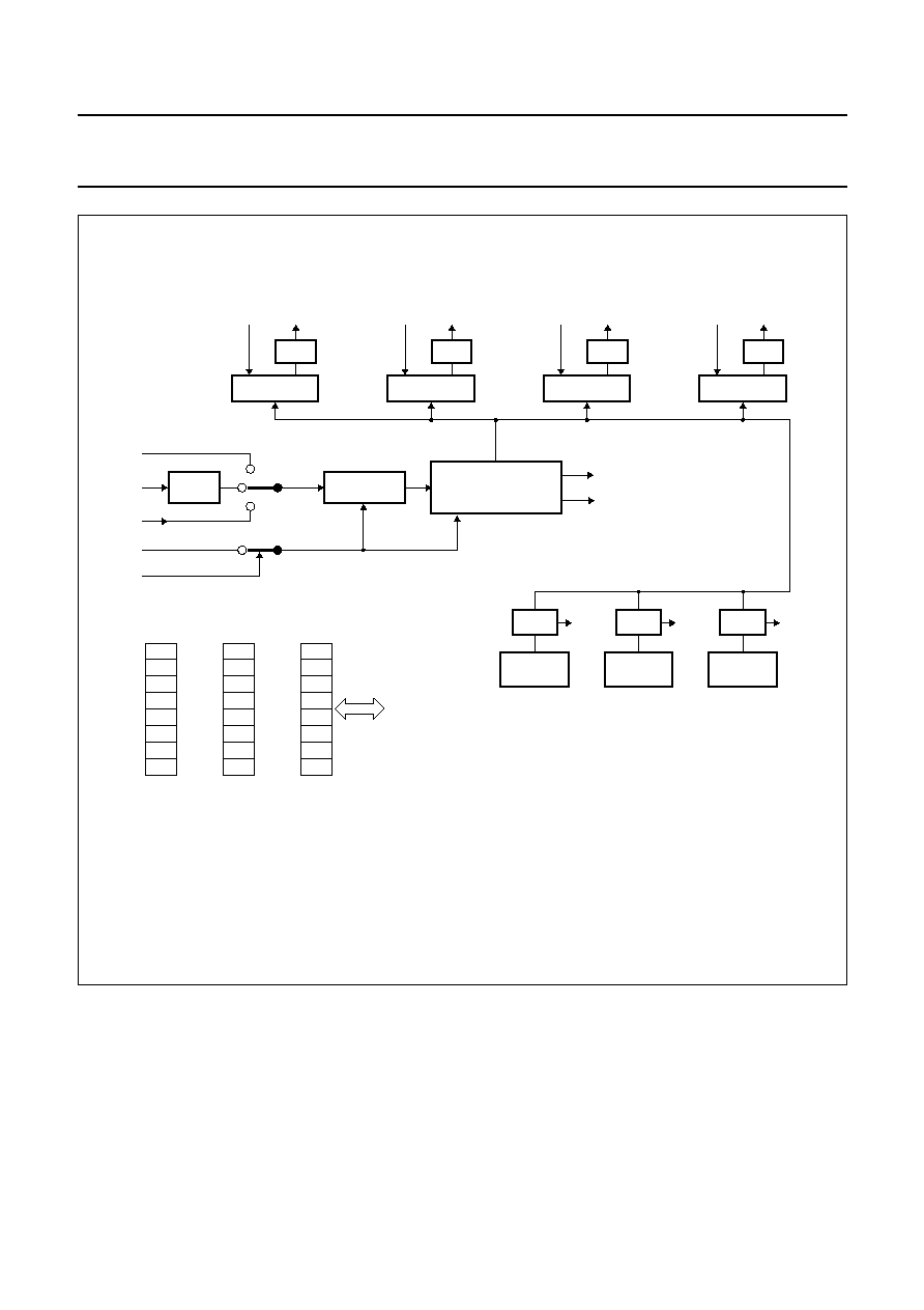
1999 Mar 12
30
Philips Semiconductors
Product specification
8-bit microcontroller
P8xC557E8
Fig.11 Block diagram of Timer 2.
handbook, full pagewidth
MGD632
STE
R
RTE
I/O port 4
= set
= reset
= toggle
= toggle status
S
R
T
TG
T2 SFR address: TML2 = lower 8 bits
TMH2 = higher 8 bits
INT
COMP
CM0 (S)
INT
COMP
CM1 (R)
INT
COMP
CM2 (T)
CT3I
INT
CTI3
CT3
off
fclk
T2
RT2
T2ER
external reset
enable
PRESCALER
1/12
T2 COUNTER
8-bit overflow interrupt
16-bit overflow interrupt
CT2I
INT
CTI2
CT2
CT1I
INT
CTI1
CT1
CT0I
INT
CTI0
CT0
R
R
R
R
R
T
T
P4.0
P4.1
P4.2
P4.3
P4.4
P4.5
P4.6
P4.7
S
S
S
S
S
S
TG
TG

1999 Mar 12
31
Philips Semiconductors
Product specification
8-bit microcontroller
P8xC557E8
12.3
Watchdog Timer (T3)
In addition to Timer T2 and the standard timers, a
Watchdog Timer (T3) consisting of an 11-bit prescaler and
an 8-bit timer is also incorporated (see Fig.12).
T3 is incremented every 1.5 ms, derived from the oscillator
frequency of 16 MHz by the following formula:
When a timer overflow occurs, the microcontroller is reset
and a reset output pulse is generated at pin RSTOUT. Also
the PLL control register is reset.
To prevent a system reset the timer must be reloaded in
time by the application software. If the processor suffers a
hardware/software malfunction, the software will fail to
reload the timer. This failure will produce a reset upon
overflow thus preventing the processor running out of
control.
f
timer
f
clk
12
2048
◊
--------------------------
=
The Watchdog Timer can only be reloaded if the condition
flag WLE = PCON.4 has been previously set by software.
At the moment the counter is loaded the condition flag is
automatically cleared.
The time interval between the timer's reloading and the
occurrence of a reset depends on the reloaded value.
For example, this may range from 1.5 ms to 0.375 s when
using an oscillator frequency of 16 MHz.
In the Idle state the Watchdog Timer and reset circuitry
remain active.
The Watchdog Timer is controlled by the watchdog enable
pin (EW). A LOW level enables the watchdog timer and
disables the Power-down mode. A HIGH level disables the
watchdog timer and enables the Power-down mode.
Fig.12 Functional diagram of T3 Watchdog Timer.
handbook, full pagewidth
MBH081
INTERNAL BUS
1/12 fclk
write
T3
PRESCALER
11-BIT
TIMER T3 (8-BIT)
LOAD
CLEAR
to reset circuitry
LOADEN
EW
LOADEN
PCON.4
PCON.1
CLEAR
WLE
PD
INTERNAL BUS
(1)
(1) See Fig.20.

1999 Mar 12
32
Philips Semiconductors
Product specification
8-bit microcontroller
P8xC557E8
13 SERIAL I/O PORTS
The P8xC557E8 is equipped with 2 independent serial
ports:
∑
SIO0, which is the full duplex UART port, identical to the
PCB80C51 serial port
∑
SIO1,which is an I
2
C-bus serial I/O interface with byte
oriented master and slave functions.
13.1
Serial I/O Port: SIO0 (UART)
SIO0 is a full duplex serial I/O port - it can transmit and
receive simultaneously. This serial port is also
receive-buffered. It can commence reception of a second
byte before the previously received byte has been read
from the receive register. If, however, the first byte has still
not been read by the time reception of the second byte is
complete, one of the bytes will be lost. The SIO0 receive
and transmit registers are both accessed via the S0BUF
special function register. Writing to S0BUF loads the
transmit register, and reading S0BUF accesses a
physically separate receive register. SIO0 can operate in
four modes:
Mode 0 Serial data is transmitted and received through
RXD. TXD outputs the shift clock. 8 data bits are
transmitted/received (LSB first). The baud rate is
fixed at
1
/
12
◊
the oscillator frequency. A write into
S0CON should be avoided during a transmission
to avoid spikes on RXD/TXD.
Mode 1 10 bits are transmitted via TXD or received
through RXD: a start bit (0), 8 data bits (LSB first),
and a stop bit (1). On receive, the stop bit is put
into RB8 of the S0CON SFR. The baud rate is
variable.
Mode 2 11 bits are transmitted through TXD or received
through RXD: a start bit (0), 8 data bits (LSB first),
a programmable 9
th
data bit, and a stop bit (1).
On transmit, the 9
th
data bit (TB8 in S0CON) can
be assigned the value of 0 or 1. With nominal
software, TB8 can be the parity bit (P in PSW).
During a receive, the 9
th
data bit is stored in RB8
(S0CON), and the stop bit is ignored. The baud
rate is programmable to either
1
/
32
or
1
/
64
of the
oscillator frequency.
Mode 3 11 bits are transmitted through TXD or received
through RXD: a start bit (0), 8 data bits (LSB first),
a programmable 9
th
data bit, and a stop bit (1).
Mode 3 is the same as Mode 2 except for the
baud rate which is variable in Mode 3.
In all four modes, transmission is initiated by any
instruction that writes to the SFR S0BUF. Reception is
initiated in Mode 0 when RI = 0 and REN = 1. In the other
three modes, reception is initiated by the incoming start bit
provided that REN = 1.
Modes 2 and 3 are provided for multiprocessor
communications. In these modes, 9 data bits are received
with the 9
th
bit written to RB8 (S0CON). The 9
th
bit is
followed by the stop bit. The port can be programmed so
that with receiving the stop bit, the serial port interrupt will
be activated if, and only if RB8 = 1.
This feature is enabled by setting bit SM2 in S0CON.
It may be used in multiprocessor systems.
For more information about how to use the UART in
combination with the registers S0CON, PCON, IE, SBUF
and the Timer register, refer to
"Data Handbook IC20".

1999 Mar 12
33
Philips Semiconductors
Product specification
8-bit microcontroller
P8xC557E8
13.1.1
S
ERIAL
P
ORT
C
ONTROL
R
EGISTER
(S0CON)
Table 43 Serial Port Control Register (address 98H)
Table 44 Description of S0CON bits
Table 45 Serial port mode select
7
6
5
4
3
2
1
0
SM0
SM1
SM2
REN
TB8
RB8
TI
RI
BIT
SYMBOL
DESCRIPTION
7
SM0
These bits are used to select the serial port mode; see Table 45.
6
SM1
5
SM2
Enables the multiprocessor communication feature in Modes 2 and 3. In these modes,
if SM2 = 1, then RI will not be activated if the received 9
th
data bit (RB8) is a logic 0.
In Mode 1, if SM2 = 1, then RI will not be activated if a valid stop bit was not received.
In Mode 0, SM2 should be a logic 0.
4
REN
Enables serial reception. Set by software to enable reception. Clear by software to
disable reception.
3
TB8
The 9
th
data bit that will be transmitted in modes 2 and 3. Set or clear by software as
desired.
2
RB8
In modes 2 and 3, RB8 is the 9
th
data bit that was received. In Mode 1, if SM2 = 0, RB8
is the stop bit that was received. In Mode 0, RB8 is not used.
1
TI
Transmit Interrupt flag. Set by hardware at the end of the 8
th
bit time in Mode 0, or at
the beginning of the stop bit in the other modes, in any serial transmission. Must be
cleared by software.
0
RI
Receive Interrupt flag. Set by hardware at the end of the 8
th
bit time in Mode 0, or
halfway through the stop bit time in the other modes, in any serial reception (except
see SM2). Must be cleared by software.
SM0
SM1
MODE
DESCRIPTION
BAUD RATE
0
0
Mode 0
Shift register
1
/
12
◊
f
clk
0
1
Mode 1
8-bit UART
variable
1
0
Mode 2
9-bit UART
1
/
64
or
1
/
32
◊
f
clk
1
1
Mode 3
9-bit UART
variable

1999 Mar 12
34
Philips Semiconductors
Product specification
8-bit microcontroller
P8xC557E8
13.2
Serial I/O Port: SIO1 (I
2
C-bus interface)
The SIO1 of the P8xC557E8 provides the fast mode,
which allows a fourth-fold increase of the bit rate up to
400 kHz. Nevertheless it is downward compatible, i.e. it
can be used in a 0 to 100 kbit/s I
2
C-bus system.
Except from the bit rate selection (see Table 48) and the
timing of the SCL and SDA signals (see Chapter 11) the
SIO circuit is the same as described in detail in the
80C51-based
"Data Handbook IC20" for the 8xC552
microcontroller.
The I
2
C-bus is a simple bidirectional 2-wire bus for efficient
inter-IC data exchange. Features of the I
2
C-bus are:
∑
Only two bus lines are required: a serial clock line (SCL)
and a serial data line (SDA)
∑
Each device connected to the bus is software
addressable by a unique address
∑
Masters can operate as master transmitter or as master
receiver
∑
It is a true multi-master bus including collision detection
and arbitration to prevent data corruption if two or more
masters simultaneously initiate data transfer
∑
Serial clock synchronization allows devices with
different bit rates to communicate via the same serial
bus
∑
ICs can be added to or removed from an I
2
C-bus system
without affecting any other circuit on the bus
∑
Fault diagnostics and debugging are simple;
malfunctions can be immediately traced.
For more information on the I
2
C-bus specification
(including fast-mode) please refer to the Philips publication
"The I
2
C-bus and how to use it" ordering number
9398 393 40011 and/or the 80C51-based
"Data Handbook IC20".
The on-chip I
2
C logic provides a serial interface that meets
the I
2
C-bus specification, supporting 4 modes of operation:
∑
Master transmitter
∑
Master receiver
∑
Slave transmitter
∑
Slave receiver.
The SIO1 logic performs a byte oriented data transport;
clock generation, address recognition and bus control
arbitration are all controlled by hardware. Via two pins the
external I
2
C-bus is interfaced to the SIO1 logic: SCL serial
clock I/O and SDA serial data I/O (SFR S1CON bit ENS1
for enabling the SIO1 logic).
The SIO1 logic handles byte transfer autonomously.
It keeps track of the serial transfers, and a status register
(S1STA) reflects the status of SIO1 and the I
2
C-bus.
Via 4 SFRs the CPU interfaces to the I
2
C-bus logic:
∑
S1CON; Serial Control Register. Bit-addressable by the
CPU
∑
S1STA; Status Register whose contents may be used
as a vector to service routines
∑
S1DAT; Data Shift Register. The data byte is stable as
long as SI = 1 (SFR S1CON)
∑
S1ADR; Slave Address Register. Its LSB
enables/disables general call address recognition.
13.2.1
S
ERIAL
C
ONTROL
R
EGISTER
(S1CON)
The CPU can read from and write to this 8-bit, directly
addressable SFR. Two bits are affected by the SIO1
hardware:
∑
the SI bit is set when a serial interrupt is requested, and
∑
the STO bit is cleared when a STOP condition is present
on the I
2
C-bus. The STO bit is also cleared when
ENS1 = 0.
When SIO1 is in a master mode, serial clock frequency is
determined by the clock rate bits CR2, CR1 and CR0.
The various bit rates are shown in Table 48.
The data shown in Table 48 do not apply to SIO1 in a slave
mode. In the slave modes, SIO1 will automatically
synchronize with any clock frequency up to 400 kHz.
However, serial clock frequencies above 100 kHz require
an oscillator frequency f
clk
of at least 12 MHz.

1999 Mar 12
35
Philips Semiconductors
Product specification
8-bit microcontroller
P8xC557E8
Table 46 Serial Control Register (address D8H)
Table 47 Description of S1CON bits
7
6
5
4
3
2
1
0
CR2
ENS1
STA
STO
SI
AA
CR1
CR0
BIT
SYMBOL
DESCRIPTION
7
CR2
Clock rate bit 2, see Table 48.
6
ENS1
Enable serial I/O. ENS1 = 0: serial I/O disabled and reset. SDA and SCL outputs are high-Z.
ENS1 = 1: serial I/O enabled.
5
STA
START flag. When this bit is set in slave mode, the hardware checks the I
2
C-bus and generates
a START condition if the bus is free or after the bus becomes free. If the device operates in
master mode it will generate a repeated START condition.
4
STO
STOP flag. If this bit is set in a master mode a STOP condition is generated. A STOP condition
detected on the I
2
C-bus clears this bit. This bit may also be set in slave mode in order to recover
from an error condition. In this case no STOP condition is generated to the I
2
C-bus, but the hard
ware releases the SDA and SCL lines and switches to the not selected receiver mode. The
STOP flag is cleared by the hardware.
3
SI
Serial Interrupt flag. This flag is set and an interrupt request is generated, after any of the
following events occur:
∑
A START condition is generated in master mode.
∑
The own slave address has been received during AA = 1.
∑
The general call address has been received while GC (bit S1ADR.0) and AA = 1.
∑
A data byte has been received or transmitted in master mode (even if arbitration is lost).
∑
A data byte has been received or transmitted as selected slave.
∑
A STOP or START condition is received as selected slave receiver or transmitter.
While the SI flag is set, SCL remains LOW and the serial transfer is suspended. SI must be
reset by software.
2
AA
Assert Acknowledge flag. When this bit is set, an acknowledge is returned after any one of the
following conditions:
∑
Own slave address is received.
∑
General call address is received; GC (bit S1ADR.0) = 1.
∑
A data byte is received, while the device is programmed to be a master receiver.
∑
A data byte is received. while the device is a selected slave receiver.
When the bit is reset, no acknowledge is returned. Consequently, no interrupt is requested when
the own address or general call address is received.
1
CR1
Clock rate bits 1 and 0; see Table 48.
0
CR0

1999 Mar 12
36
Philips Semiconductors
Product specification
8-bit microcontroller
P8xC557E8
Table 48 Selection of I
2
C-bus bit rate
Note
1. These bit rates are for `fast-mode' I
2
C-bus applications and cannot be used for standard I
2
C bit rates up to
100 kbits/s.
CR2
CR1
CR0
BIT RATE (kbits/s) at f
clk
12 MHz
16 MHz
1
0
0
50
66.7
1
0
1
3.75
5
1
1
0
75
100
1
1
1
100
-
0
0
0
200
(1)
266.7
(1)
0
0
1
7.5
10
0
1
0
300
(1)
400
(1)
0
1
1
400
(1)
-
MLB199
SLAVE ADDRESS
S1ADR
GC
SHIFT REGISTER
S1DAT
SDA
ARBITRATION SYNC LOGIC
SCL
BUS CLOCK GENERATOR
S1STA
INTERNAL BUS
7
0
S1CON
7
0
7
0
7
0
CONTROL REGISTER
STATUS REGISTER
Fig.13 Block diagram of I
2
C serial I/O interface.

1999 Mar 12
37
Philips Semiconductors
Product specification
8-bit microcontroller
P8xC557E8
13.2.2
S
ERIAL
S
TATUS
R
EGISTER
(S1STA)
The contents of this register may be used as a vector to a service routine. This optimizes the response time of the
software and consequently that of the I
2
C-bus. S1STA is a read-only register. The status codes for all possible modes
of the I
2
C-bus interface are given in Tables 51 to 55.
Table 49 Serial status register (address D9H)
Table 50 Description of S1STA bits
Table 51 MST/TRX mode
Table 52 MST/REC mode
7
6
5
4
3
2
1
0
SC4
SC3
SC2
SC1
SC0
0
0
0
BIT
SYMBOL
DESCRIPTION
7 to 3
SC4 to SC0
5-bit status code.
2 to 0
-
These 3 bits are held LOW (for service routine vector increment 8).
S1STA VALUE
DESCRIPTION
08H
A START condition has been transmitted.
10H
A repeated START condition has been transmitted.
18H
SLA and W have been transmitted, ACK has been received.
20H
SLA and W have been transmitted, ACK received.
28H
DATA and S1DAT has been transmitted, ACK received.
30H
DATA and S1DAT has been transmitted, ACK received.
38H
Arbitration lost in SLA, R/W or DATA.
S1STA VALUE
DESCRIPTION
38H
Arbitration lost while returning ACK.
40H
SLA and R have been transmitted, ACK received.
48H
SLA and R have been transmitted, ACK received.
50H
DATA has been received, ACK returned.
58H
DATA has been received, ACK returned.

1999 Mar 12
38
Philips Semiconductors
Product specification
8-bit microcontroller
P8xC557E8
Table 53 SLV/REC mode
Table 54 SLV/TRX mode
Table 55 Miscellaneous
Table 56 Symbols used in Tables 51 to 55
S1STA VALUE
DESCRIPTION
60H
Own SLA and W have been received, ACK returned.
68H
Arbitration lost in SLA, R/W as MST. Own SLA and W have been received, ACK returned.
70H
General CALL has been received, ACK returned.
78H
Arbitration lost in SLA, R/W as MST. General call has been received.
80H
Previously addressed with own SLA. DATA byte received, ACK returned.
88H
Previously addressed with own SLA. DATA byte received, ACK returned.
90H
Previously addressed with general call. DATA byte has been received, ACK has been returned.
98H
Previously addressed with general call. DATA byte has been received, ACK has been returned.
A0H
A STOP condition or repeated START condition has been received while still addressed as SLV/REC
or SLV/TRX.
S1STA VALUE
DESCRIPTION
A8H
Own SLA and R have been received, ACK returned.
B0H
Arbitration lost in SLA, R/W as MST. Own SLA and R have been received, ACK returned.
B8H
DATA byte has been transmitted, ACK returned.
C0H
DATA byte has been transmitted, ACK returned.
C8H
Last DATA byte has been transmitted (AA = logic 0), ACK received.
S1STA VALUE
DESCRIPTION
00H
Bus error during MST mode or selected SLV mode, due to an erroneous START or STOP condition.
F8H
No relevant information available, SI not set.
SYMBOL
DESCRIPTION
SLA
7-bit slave address
R
read bit
W
write bit
ACK
acknowledgement (acknowledge bit = logic 0)
ACK
no acknowledgement (acknowledge bit = logic 1)
DATA
8-bit data byte to or from I
2
C-bus
MST
master
SLV
slave
TRX
transmitter
REC
receiver

1999 Mar 12
39
Philips Semiconductors
Product specification
8-bit microcontroller
P8xC557E8
13.2.3
D
ATA
S
HIFT
R
EGISTER
(S1DAT)
This register contains the serial data to be transmitted or data which has been received. Bit 7 is transmitted or received
first; i.e. data is shifted from right to left.
Table 57 Data Shift Register (address DAH)
13.2.4
A
DDRESS
R
EGISTER
(S1ADR)
This 8-bit register may be loaded with the 7-bit slave address to which the controller will respond when programmed as
a slave receiver/transmitter.
Table 58 Address Register (address DBH)
Table 59 Description of S1ADR bits
7
6
5
4
3
2
1
0
S1DAT.7
S1DAT.6
S1DAT.5
S1DAT.4
S1DAT.3
S1DAT.2
S1DAT.1
S1DAT.0
7
6
5
4
3
2
1
0
SLA6
SLA5
SLA4
SLA3
SLA2
SLA1
SLA0
GC
BIT
SYMBOL
DESCRIPTION
7 to 1
SLA6 to SLA0 Own slave address.
0
GC
This bit is used to determine whether the general call address is recognized. When
GC = 0, the general call address is not recognized; when GC = 1, the general call
address is recognized.

1999 Mar 12
40
Philips Semiconductors
Product specification
8-bit microcontroller
P8xC557E8
14 INTERRUPT SYSTEM
External events and the real-time-driven on-chip
peripherals require service by the CPU asynchronously to
the execution of any particular section of code. To tie the
asynchronous activities of these functions to normal
program execution a multiple-source, two-priority-level,
nested interrupt system is provided. Interrupt response
time in a single-interrupt system is in the range
2.25
µ
s to 6.75
µ
s when using a 16 MHz crystal.
The latency time depends on the sequence of instructions
executed directly after an interrupt request.
The P8xC557E8 acknowledges interrupt requests from
15 sources as follows (see Fig.14):
∑
INT0 and INT1 external interrupts
∑
Timer 0 and Timer 1 internal timer/counter interrupts
∑
Timer 2 internal timer/counter byte and/or 16-bit
overflow, 3 compare and 4 capture interrupts (or
4 additional external interrupts).
Note that if a capture register is unused and its contents
are of no interest, then the corresponding input pin
CTnI/P1.n (n = 0 to 3) may be used as a (configurable)
positive and/or negative edge triggered additional
external interrupt input (INT2, INT3, INT4 and INT5).
∑
UART serial I/O port receive/transmit interrupt
∑
I
2
C-bus interface serial I/O interrupt
∑
ADC autoscan completion interrupt
∑
`Seconds' timer interrupt SEC (ORed with INT1); for
details please refer to Chapter 16.2.4.
The External Interrupts INT0 and INT1 can each be either
level-activated or transition-activated, depending on bits
IT0 and IT1 in register TCON. The flags that actually
generate these interrupts are bits IE0 and IE1 in TCON.
When an external interrupt is generated, the
corresponding request flag is cleared by the hardware
when the service routine is vectored to, only if the interrupt
was transition-activated. If the interrupt was level-activated
then the interrupt request flag remains set until the external
interrupt pin INTn goes HIGH. Consequently, the external
source has to hold the request active until the requested
interrupt is actually generated. Then it has to deactivate
the request before the interrupt service routine is
completed, or else another interrupt will be generated.
As these external interrupts are active LOW a `wire-ORing'
of several interrupt sources to one input pin allows
expansion.
The Timer 0 and Timer 1 interrupts are generated by TF0
and TF1, which are set by a roll-over in their respective
timer/counter register (except for Timer 0 in Mode 3 of the
serial interface). When a Timer interrupt is generated, the
flag that generated it is cleared by the on-chip hardware
when the service routine is vectored to.
The eight Timer/Counter T2 Interrupt sources are:
4 capture Interrupts (1), 3 compare interrupts and an
overflow interrupt. The appropriate interrupt request flags
must be cleared by software.
The UART Serial Port Interrupt is generated by the logical
OR of RI and TI (register S0CON). Neither of these flags
is cleared by hardware. The service routine will normally
have to determine whether it was RI or TI that generated
the interrupt, and the bit will have to be cleared by
software.
The I
2
C Interrupt is generated by bit SI in register S1CON.
This flag has to be cleared by software.
The ADC Interrupt is generated by bit ADINT, which is set
when the conversion of all selected analog inputs to be
scanned is finished. ADINT must be cleared by software.
It cannot be set by software.
The `seconds' timer Interrupt is generated by bit SECINT
in register PLLCON. This flag has to be cleared by
software. Note that the `seconds' timer can only be used
with the 32 kHz PLL oscillator.
All of the bits that generate interrupts can be set or cleared
by software, with the same result as though they had been
set or cleared by hardware (except the ADC interrupt
request flag ADINT, which cannot be set by software).
That is, interrupts can be generated or pending interrupts
can be cancelled in software.
The Interrupts X0, T0, X1, T1, SEC, S0 and S1 are able to
terminate the Idle mode.
14.1
Interrupt Enable Registers
Each interrupt source can be individually enabled or
disabled by setting or clearing a bit in the interrupt enable
Special Function Registers IEN0 and IEN1. All interrupt
sources can also be globally disabled by clearing bit EA in
IEN0. The interrupt enable registers are described in
Tables 62 and 64.

1999 Mar 12
41
Philips Semiconductors
Product specification
8-bit microcontroller
P8xC557E8
14.2
Interrupt Handling
The interrupt sources are sampled at S5P2 of every
machine cycle. The samples are polled during the
following machine cycle. If one of the flags was in a set
condition at S5P2 of the previous machine cycle, the
polling cycle will detect it and the interrupt system will
generate an LCALL to the appropriate service routine,
provided this hardware generated LCALL is not blocked by
any of the following conditions:
1. An interrupt of higher or equal priority level is already
in progress.
2. The current machine cycle is not the final cycle in the
execution of the instruction in progress. (No interrupt
request will be serviced until the instruction in progress
is completed.).
3. The instruction in progress is RETI or any access to
the interrupt priority or interrupt enable registers.
(No interrupt will be serviced after RETI or after a read
or write to IP0, IP1, IE0, or IE1 until at least one other
instruction has been subsequently executed.).
The polling cycle is repeated every machine cycle, and the
values polled are the values present at S5P2 of the
previous machine cycle. Note that if an interrupt flag is
active but is not being responded to because of one of the
above conditions, and if the flag is inactive when the
blocking condition is removed, then the blocked interrupt
will not be serviced. Thus, the fact that the interrupt flag
was once active but not serviced is not remembered.
Every polling cycle is new.
The processor acknowledges an interrupt request by
executing a hardware-generated LCALL to the appropriate
service routine. In some cases it also clears the flag which
generated the interrupt, and in others it does not. It clears
the Timer 0, Timer 1, and external interrupt flags.
An external interrupt flag (IE0 or IE1) is cleared only if it
was transition-activated. All other interrupt flags are not
cleared by hardware and must be cleared by the software.
The LCALL pushes the contents of the program counter on
to the stack (but it does not save the PSW) and reloads the
PC with an address that depends on the source of the
interrupt being vectored to as shown in Table 60.
Execution proceeds from the vector address until the RETI
instruction is encountered. The RETI instruction clears the
`priority level active' flip-flop that was set when this
interrupt was acknowledged. It then pops the top two bytes
from the stack and reloads the program counter. Execution
of the interrupted program continues from where it was
interrupted.
14.3
Interrupt Priority Structure
Each interrupt source can be assigned one of two priority
levels: high and low. Interrupt priority levels are defined by
the interrupt priority SFRs IP0 and IP1, which are
described in Tables 66 and 68.
Interrupt priority levels are as follows:
logic 0 = low priority
logic 1 = high priority.
A low priority interrupt may be interrupted by a high priority
interrupt. A high priority interrupt cannot be interrupted by
any other interrupt source. If two requests of different
priority occur simultaneously, the high priority level request
is serviced. If requests of the same priority are received
simultaneously, an internal polling sequence determines
which request is serviced. Thus, within each priority level,
there is a second priority structure determined by the
polling sequence. This second priority structure is shown
in Table 60.
14.4
Interrupt vectors
The vector indicates the Program Memory location where
the appropriate interrupt service routine starts; Table 60.
Table 60 Interrupt vectors and priority structure
Note
1. X0 has the highest priority; T2 the lowest.
SOURCE
SYMBOL
(1)
VECTOR
ADDRESS
(HEX)
External 0
X0 (highest)
0003
Serial I/O: SIO1 (I
2
C-bus)
S1
002B
ADC completion
ADC
0053
Timer 0 overflow
T0
000B
T2 capture 0
CT0
0033
T2 compare 0
CM0
005B
External 1/ seconds interrupt X1/SEC
0013
T2 capture 1
CT1
0033
T2 compare 1
CM1
0063
Timer 1 overflow
T1
001B
T2 capture 2
CT2
0043
T2 compare 2
CM2
006B
Serial I/O SIO0 (UART)
S0
0023
T2 capture 3
CT3
004B
T2 overflow
T2 (lowest)
0073

1999 Mar 12
42
Philips Semiconductors
Product specification
8-bit microcontroller
P8xC557E8
Fig.14 Interrupt system.
handbook, full pagewidth
interrupt
sources
source enable
global enable
interrupt enable registers
a1
a2
b1
b2
c1
c2
d1
d2
e1
e2
f1
f2
g1
g2
h1
h2
i1
i2
j1
j2
k1
k2
l1
l2
m1
m2
n1
n2
o1
o2
interrupt priority
registers
a1
SOURCE
IDENTIFICATION
vector
b1
c1
d1
e1
f1
g1
h1
i1
j1
k1
l1
m1
n1
o1
high
priority
interrupt
request
MBC754
a2
SOURCE
IDENTIFICATION
vector
b2
c2
d2
e2
f2
g2
h2
i2
j2
k2
l2
m2
n2
o2
low
priority
interrupt
request
polling hardware
CT3I
CT2I
CT1I
CT0I
INT0
INT1
EXTERNAL
INTERRUPT
REQUEST 0
ADC
TIMER 0
OVERFLOW
TIMER 2
CAPTURE 0
TIMER 2
COMPARE 0
EXTERNAL
INTERRUPT
REQUEST 1
TIMER 2
CAPTURE 1
TIMER 2
COMPARE 1
TIMER 1
OVERFLOW
TIMER 2
CAPTURE 2
TIMER 2
COMPARE 2
UART
SERIAL
PORT
TIMER 2
CAPTURE 3
TIMER T2
OVERFLOW
T
R
I
2
C-BUS
SERIAL
PORT
1999 Mar 12
43
Philips Semiconductors
Product specification
8-bit microcontroller
P8xC557E8
14.5
Interrupt Enable and Priority Registers
14.5.1
I
NTERRUPT
E
NABLE
R
EGISTER
0 (IEN0)
Logic 0 = interrupt disabled; logic 1 = interrupt enabled.
Table 61 Interrupt Enable Register 0 (address A8H)
Table 62 Description of IEN0 bits
14.5.2
I
NTERRUPT
E
NABLE
R
EGISTER
1 (IEN1)
Logic 0 = interrupt disabled; logic 1 = interrupt enabled.
Table 63 Interrupt Enable Register 1 (address E8H)
Table 64 Description of IEN1 bits
7
6
5
4
3
2
1
0
EA
EAD
ES1
ES0
ET1
EX1
ET0
EX0
BIT
SYMBOL
DESCRIPTION
7
EA
General enable/disable control. If bit EA is:
LOW, then no interrupt is enabled.
HIGH, then any individually enabled interrupt will be accepted.
6
EAD
Enable ADC interrupt.
5
ES1
Enable SIO1 (I
2
C-bus) interrupt.
4
ES0
Enable SIO0 (UART) interrupt.
3
ET1
Enable Timer 1 interrupt.
2
EX1
Enable External 1 interrupt / Seconds interrupt.
1
ET0
Enable Timer 0 interrupt.
0
EX0
Enable External 0 interrupt.
7
6
5
4
3
2
1
0
ET2
ECM2
ECM1
ECM0
ECT3
ECT2
ECT1
ECT0
BIT
SYMBOL
DESCRIPTION
7
ET2
Enable T2 overflow interrupt(s).
6
ECM2
Enable T2 comparator 2 interrupt.
5
ECM1
Enable T2 comparator 1 interrupt.
4
ECM0
Enable T2 comparator 0 interrupt.
3
ECT3
Enable T2 capture register 3 interrupt.
2
ECT1
Enable T2 capture register 2 interrupt.
1
ECT1
Enable T2 capture register 1 interrupt.
0
ECT0
Enable T2 capture register 0 interrupt.

1999 Mar 12
44
Philips Semiconductors
Product specification
8-bit microcontroller
P8xC557E8
14.5.3
I
NTERRUPT
P
RIORITY
R
EGISTER
0 (IP0)
Logic 0 = low priority; logic 1 = high priority.
Table 65 Interrupt Priority Register 0 (address B8H)
Table 66 Description of IP0 bits
14.5.4
I
NTERRUPT
P
RIORITY
R
EGISTER
1 (IP1)
Logic 0 = low priority; logic 1 = high priority.
Table 67 Interrupt Priority Register 1 (address F8H)
Table 68 Description of IP1 bits
7
6
5
4
3
2
1
0
-
PAD
PS1
PS0
PT1
PX1
PT0
PX0
BIT
SYMBOL
DESCRIPTION
7
-
Reserved for future use.
6
PAD
ADC interrupt priority level.
5
PS1
SIO1 (I
2
C-bus) interrupt priority level.
4
PS0
SIO0 (UART) interrupt priority level.
3
PT1
Timer 1 interrupt priority level.
2
PX1
External interrupt 1/Seconds priority level.
1
PT0
Timer 0 interrupt priority level.
0
PX0
External interrupt 0 priority level.
7
6
5
4
3
2
1
0
PT2
PCM2
PCM1
PCM0
PCT3
PCT2
PCT1
PCT0
BIT
SYMBOL
DESCRIPTION
7
PT2
T2 overflow interrupt(s) priority level.
6
PCM2
T2 comparator 2 priority interrupt level.
5
PCM1
T2 comparator 1 priority interrupt level.
4
PCM0
T2 comparator 0 priority interrupt level.
3
PCT3
T2 capture register 3 priority interrupt level.
2
PCT2
T2 capture register 2 priority interrupt level.
1
PCT1
T2 capture register 1 priority interrupt level.
0
PCT0
T2 capture register 0 priority interrupt level.

1999 Mar 12
45
Philips Semiconductors
Product specification
8-bit microcontroller
P8xC557E8
15 REDUCED POWER MODES
Two software-selectable modes of reduced power
consumption are implemented: Idle and Power-down
mode. These modes are activated by software via SFR
PCON.
15.1
Idle mode
Idle mode operation permits the interrupt, serial ports and
timer blocks T0, T1 and T3 to function while the CPU is
halted. The functions that are switched off when the
microcontroller enters the Idle mode are:
∑
CPU (halted)
∑
Timer 2 (stopped and reset)
∑
PWM0, PWM1 (reset, output = HIGH)
∑
ADC (aborted if conversion in progress).
The functions that remain active during Idle mode may
generate an interrupt or reset and thus terminate the
Idle mode. These functions are:
∑
Timer 0, Timer 1, Timer 3 (Watchdog Timer)
∑
UART
∑
I
2
C
∑
External interrupt
∑
Seconds timer.
The instruction that sets PCON.0 is the last instruction
executed in the normal operating mode before Idle mode
is activated.
Once in the Idle mode, the CPU status is preserved in its
entirety: the Stack Pointer, Program Counter, Program
Status Word, Accumulator, RAM and all other registers
maintain their data during Idle mode. The status of
external pins during Idle mode is shown in Table 69.
There are three ways to terminate the Idle mode:
∑
Activation of any enabled interrupt X0, T0, X1, SEC, T1,
S0 or S1 will cause PCON.0 to be cleared by hardware
terminating Idle mode but only, if there is no interrupt in
service with the same or higher priority. The interrupt is
serviced, and following return from interrupt instruction
RETI, the next instruction to be executed will be the one
which follows the instruction that wrote a logic 1 to
PCON.0.
The flag bits GF0 and GF1 may be used to determine
whether the interrupt was received during normal
execution or during Idle mode.
For example, the instruction that writes to PCON.0 can
also set or clear one or both flag bits.
When Idle mode is terminated by an interrupt, the
service routine can examine the status of the flag bits.
∑
The second way of terminating the Idle mode is with an
external hardware reset. Since the oscillator is still
running, the hardware reset is required to be active for
two machine cycles (24 HF oscillator periods) to
complete the reset operation if the HF oscillator is
selected.
When the PLL oscillator is selected a hardware reset of
1
µ
s (but no longer than 10 ms) is required and the
microcontroller will typically restart within 63 ms after the
reset has finished.
∑
The third way of terminating the Idle mode is by internal
watchdog reset. The microcontroller restarts after three
machine cycles in all cases.
15.2
Power-down mode
In Power-down mode the system clock is halted. If the PLL
oscillator is selected (SELXTAL1 = 0) and the RUN32 bit
is set, the 32 kHz oscillator keeps running, otherwise it is
stopped. If the HF oscillator (SELXTAL1 = 1) is selected,
it is stopped after setting the bit PD in the PCON register.
The instruction that sets PCON.1 is the last executed prior
to going into the Power-down mode. Once in
Power-down mode, the HF oscillator is stopped.
The 32 kHz oscillator may remain active. The contents of
the on-chip RAM and the Special Function Registers are
preserved.
Note that the Power-down mode can not be entered when
the Watchdog Timer has been enabled.
The Power-down mode can be terminated by an external
reset in the same way as in the 80C51 (RAM is saved, but
SFRs are cleared due to reset) or in addition by any one of
the external interrupts (INT0, INT1) or Seconds interrupt.
The status of the external pins during Power-down mode
is shown in Table 69. If the Power-down mode is activated
while in external Program Memory, the port data that is
held in the Special Function Register P2 is restored to
Port 2. If the data is a logic 1, the port pin is held HIGH
during the Power-down mode by the strong pull-up
transistor P1 (see Fig.8).
The Power-down mode should not be entered within an
interrupt routine because Wake-up with an external or
`Seconds' interrupt is not possible in that case.
1999 Mar 12
46
Philips Semiconductors
Product specification
8-bit microcontroller
P8xC557E8
15.3
Wake-up from Power-down mode
The Power-down mode of the P8xC557E8 can also be
terminated by any one of the three enabled interrupts,
INT0, INT1 or Seconds interrupt.
If there is an interrupt already in service, which has same
or higher priority than the Wake-up interrupt,
Power-down mode will switch over to Idle mode and stay
there until an interrupt of higher priority terminates
Idle mode.
A termination with these interrupts does not affect the
internal Data Memory and does not affect the Special
Function Registers. This gives the possibility to exit
Power-down without changing the port output levels.
To terminate the Power-down mode with an external
interrupt, INT0 or INT1 must be switched to be
level-sensitive and must be enabled. The external interrupt
input signal INT0 or INT1 must be kept LOW till the
oscillator has restarted and stabilized (see Fig.15).
A Seconds interrupt will terminate the Power-down mode
if it is enabled and INT1 is level sensitive. In order to
prevent any interrupt priority problems during Wake-up,
the priority of the desired Wake-up interrupt should be
higher than the priorities of all other enabled interrupt
sources.
The instruction following the one that put the device into
the Power-down mode will be the first one which will be
executed after the interrupt routine has been serviced.
15.4
Status of external pins
Table 69 Status of external pins during Idle and Power-down modes
Note
1. In Idle mode SCL and SDA can be active as outputs only if SIO1 is enabled; if SIO1 is disabled (S1CON.6/ENS1 = 0)
these pins are in a high-impedance state.
MODE
MEMORY
ALE PSEN
PWM0/
PWM1
PORT0
PORT1
PORT2
PORT3
PORT4
SCL/ SDA
Idle
internal
1
1
1
port data port data port data port data port data operative
(1)
external
1
1
1
high-Z
port data address
port data port data operative
(1)
Power-down internal
0
0
1
port data port data port data port data port data
high-Z
external
0
0
1
high-Z
port data port data port data port data
high-Z
Fig.15 Wake-up by interrupt.
handbook, full pagewidth
MBH083
oscillator start-up time
interrupts are polled
Idle mode
LCALL
interrupt routine
>
560 ms
Power-down mode
internal timing stopped
32 kHz oscillator stopped
>
10 ms
32 kHz oscillator running
XTAL1, 2 oscillator stopped
C1
INT0
INT1
C1
C1
C2
set external interrupt latch
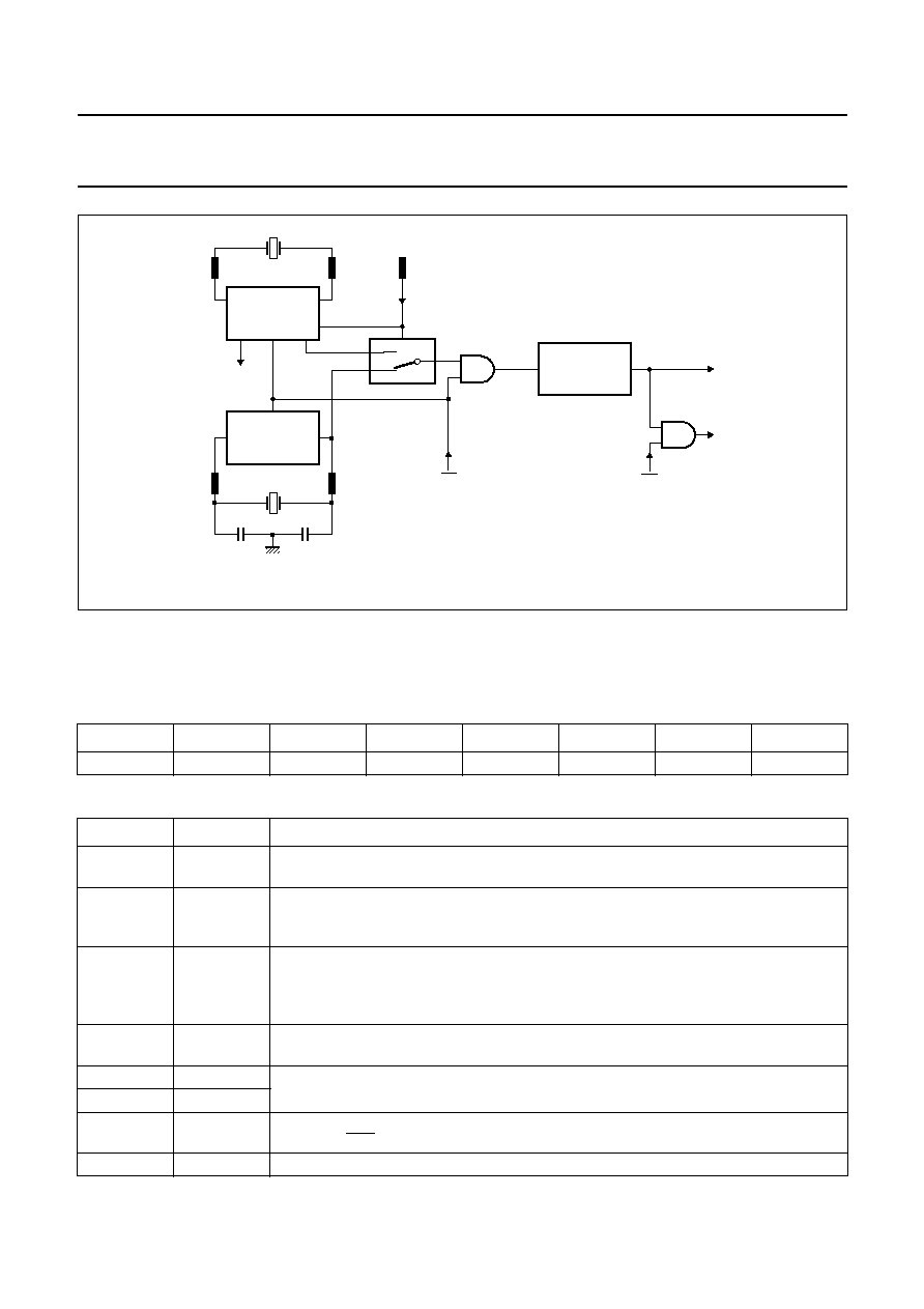
1999 Mar 12
47
Philips Semiconductors
Product specification
8-bit microcontroller
P8xC557E8
15.5
Power Control Register (PCON)
PCON is not bit addressable and the value after reset is 00H.
Table 70 Power Control Register (address 87H)
Table 71 Description of PCON bits
7
6
5
4
3
2
1
0
SMOD
ARD
RFI
WLE
GF1
GF0
PD
IDL
BIT
SYMBOL
DESCRIPTION
7
SMOD
Double Baud rate. When set to logic 1 the baud rate is doubled when the serial port
SIO0 is being used in Modes 1, 2 and 3.
6
ARD
AUX-RAM disable. When set to logic 1 the internal 1792 bytes AUX-RAM is disabled,
so that all MOVX-Instructions access the external Data Memory - as it is with the
standard 80C51.
5
RFI
RFI-Reduction Mode. When set to HIGH the toggling of ALE pin is prohibited. This bit
is cleared on reset and can be set and cleared by software. When set, ALE pin will be
pulled down internally, switching an external address latch to a quiet state. See also
Sections 2.1 and 6.2.
4
WLE
Watchdog Load Enable. This flag must be set by software prior to loading T3
(Watchdog Timer). It is cleared when T3 is loaded.
3
GF1
General purpose flag bits.
2
GF0
1
PD
Power-down mode select. Setting this bit activates Power-down mode. It can only be
set if input EW is HIGH.
0
IDL
Idle mode select. Setting this bit activates the Idle mode.
Fig.16 Idle and Power-down hardware for clock generation.
handbook, full pagewidth
MBH082
PLL
OCSILLATOR
CLOCK
GENERATOR
OCSILLATOR
'second'
timer
32 kHz
PD
XTAL3
XTAL3
SELXTAL1
3.5 to 16 kHz
XTAL2
XTAL1
fclk
IDL
interrupts,
serial
ports
T0, T1, T3
CPU
T2
ADC
PWM

1999 Mar 12
48
Philips Semiconductors
Product specification
8-bit microcontroller
P8xC557E8
16 OSCILLATOR CIRCUITS
16.1
XTAL1; XTAL2 oscillator: standard 80C51
The XTAL1; XTAL2 oscillator: standard 80C51 is selected
when input SELXTAL1 = 1. The oscillator circuit is a
single-stage inverting amplifier in a Pierce oscillator
configuration. The circuitry between pins XTAL1 and
XTAL2 is basically an inverter biased to the transfer point.
Either a crystal or ceramic resonator can be used as the
feedback element to complete the oscillator circuitry. Both
are operated in parallel resonance.
XTAL1 is the high gain amplifier input, and XTAL2 is the
output; see Fig.17. To drive the P8xC557E8 externally,
XTAL1 is driven from an external source and XTAL2 is left
open-circuit; see Fig.18.
When the `XTAL1; XTAL2 oscillator' is selected the
`XTAL3; XTAL4 oscillator' is halted; pins XTAL3 and
XTAL4 must not be connected.
16.2
XTAL3; XTAL4 oscillator: 32 kHz PLL oscillator
(with Seconds timer)
The XTAL3; XTAL4 oscillator: 32 kHz oscillator and the
Phase Locked Loop (PLL) are selected when
SELXTAL1 = 0 (XTAL1; XTAL2 oscillator is halted). In this
case pin XTAL2 is kept floating.
16.2.1
32
K
H
Z OSCILLATOR
The 32 kHz oscillator consists of an inverter, which forms
a Pierce oscillator with the on-chip components C1, C2, R
f
and an external crystal of 32768 Hz. The inverter is
switched to 3-state and pin XTAL3 is pulled to V
SS
:
∑
During Power-down mode, when RUN32
(PLLCON.7) = 0
∑
During reset, RSTIN = 1
∑
When the XTAL1; XTAL2 oscillator is selected
(SELXTAL1 = 1).
16.2.2
PLL C
URRENT
C
ONTROLLED
O
SCILLATOR
A Current Controlled Oscillator (CCO) generates a clock
frequency f
CCO
of approximately 32, 38, 44 or 50 MHz.
This CCO is controlled by the PLL, with the 32 kHz
oscillator as the reference clock.
The system clock frequency f
clk
is derived from f
CCO
and
can be varied under software control by changing the
contents of the PLL Control Register (PLLCON) bits
FSEL.4 to FSEL.0. The CCO frequency f
CCO
can be
changed via the PLLCON bits FSEL.1 and FSEL.0 and the
maximum locking time is 10 ms (this parameter is
characterized). During the stabilization phase, no time
critical routines should be executed.
Changing f
clk
has to be done in two steps:
∑
From high to low frequencies; first change
FSEL.4 to FSEL.2, then FSEL.1 to FSEL.0
∑
From low to high frequencies; first change
FSEL.1 to FSEL.0 only, and after a stabilization phase
of 10 ms, change FSEL.4 to FSEL.2.
If only FSEL.4 to FSEL.2 is changed, and FSEL.1 to
FSEL.0 not, then it takes approximately 1
µ
s until the new
frequency is available. The frequency selection is shown in
Table 73.
16.2.3
PLL C
ONTROL
R
EGISTER
(PLLCON)
PLLCON is a Special Function Register, which can be
read and written by software. It contains the control bits:
∑
to select the system clock frequencies (f
clk
)
∑
the seconds interrupt flag (SECINT)
∑
to enable the seconds interrupt flag (ENSECI)
∑
the RUN32 bit, which defines if during Power-down
mode the 32 kHz oscillator is halted or not.
PLLCON is initialized to 0DH upon reset (RSTIN = 1) or
Watchdog Timer overflow. PLLCON = 0DH corresponds
to a system clock frequency f
clk
= 11.01 MHz.
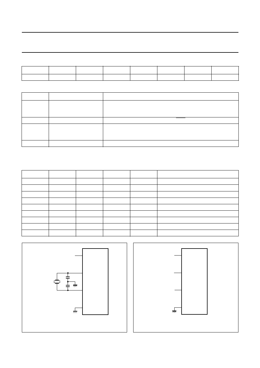
1999 Mar 12
49
Philips Semiconductors
Product specification
8-bit microcontroller
P8xC557E8
Table 72 PLL Control Register (address F9H)
Table 73 Description of PLLCON bits
Table 74 System clock frequency (f
clk
) selection
Other combinations than mentioned in this table, are reserved and may not be selected. This allows to generate the
standard baudrates 19200, 9600, 4800, 2400 and 1200 Baud, when using the UART and Timer 1.
7
6
5
4
3
2
1
0
RUN32
ENSECI
SECINT
FSEL.4
FSEL.3
FSEL.2
FSEL.1
FSEL.0
BIT
SYMBOL
DESCRIPTION
7
RUN32
If RUN32 = 0, then the 32 kHz oscillator is halted during Power-down
mode. If RUN32 = 1, then the 32 kHz oscillator remains active during
Power-down mode.
6
ENSECI
Enable the seconds interrupt; enabling INT1 is also required.
5
SECINT
Seconds interrupt requested by an overflow of the seconds timer (which
occurs every second) or via writing a logic 1 to this bit. SECINT can only
be cleared by writing a logic 0 to this bit.
4 to 0
FSEL.4 to FSEL.0
System clock frequency selection bits; see Table 74.
FSEL.4
FSEL.3
FSEL.2
FSEL.1
FSEL.0
f
CLK
(MHz)
1
0
0
1
1
3.93
0
1
1
1
1
7.86
0
1
0
1
1
15.73
1
0
0
1
0
4.72
0
1
1
1
0
9.44
1
0
0
0
1
5.51
0
1
1
0
1
11.01
1
0
0
0
0
6.29
0
1
1
0
0
12.58
handbook, halfpage
MBH084
C1
HIGH
C2
C1 = C2 = 20 pF
quartz crystal
or ceramic
resonator
VSS
XTAL2
XTAL1
SELXTAL1
Fig.17 Using the on-chip oscillator.
handbook, halfpage
MBH085
HIGH
n.c.
external
clock
signal
VSS
XTAL2
XTAL1
SELXTAL1
Fig.18 Using an external clock.
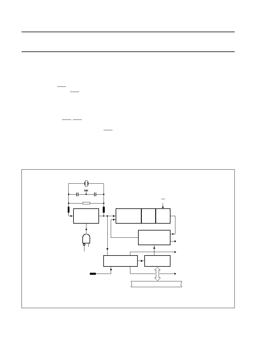
1999 Mar 12
50
Philips Semiconductors
Product specification
8-bit microcontroller
P8xC557E8
16.2.4
S
ECONDS
T
IMER
This counter provides an overflow signal every second,
when the 32 kHz oscillator is running. The overflow output
sets the interrupt flag SECINT. This interrupt can be
disabled/enabled by ENSECI. If SECINT is enabled, it is
logically ORed with INT1 (External interrupt 1).
The `seconds' interrupt and INT1 therefore share the same
priority and vector. The software has to check both flags
SECINT (PLLCON.5) and IE1 (TCON.3) to distinguish
between the two interrupt sources. SECINT can only be
cleared via writing a logic 0 to this bit.
The external interrupts INT0, INT1 or the seconds interrupt
can wake-up the PLL oscillator and the microcontroller as
described in Chapter 15.3. For a wake-up via INT1 or
seconds interrupt, IE1 must be enabled and
level-sensitive.
A further function of the seconds timer is to control the
start-up timing of the microcontroller after reset or after
wake-up from Power-down.
It controls the stretching of the reset pulse to the
microcontroller and controls releasing the system clock to
the microcontroller. A RSTIN signal of 1
µ
s at minimum will
reset the microcontroller.
∑
In the even of reset or wake-up with halted 32 kHz
oscillator: from RSTIN falling edge or wake-up interrupt
it takes 560 ms at maximum for the start-up of the
32 kHz oscillator itself and the stabilization of the PLLs.
∑
In the event of wake-up with running 32 kHz oscillator:
from wake-up interrupt it takes about 10 ms for the
stabilization of the PLLs.
After this start-up time, the microcontroller is supplied with
the system clock and - in case of a reset - the internally
stretched reset signal overlaps about 45
µ
s, to guarantee
a proper initialization of the microcontroller.
For further information refer to Chapter 15.
Fig.19 Block diagram PLL.
handbook, full pagewidth
MBH086
32 kHz
OCSILLATOR
PHASE
COMPARATOR
Rf
C1
C2
LOOP
FILTER
CCO
32.768 kHz
XTAL3
XTAL4
PROGRAMMABLE
DIVIDER
PLLCON
SECONDS TIMER
PD
PD
RUN32
RSTIN
INTERNAL BUS
'seconds'
interrupt
request
reset to
controller
system
clock
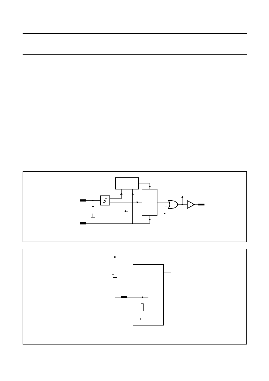
1999 Mar 12
51
Philips Semiconductors
Product specification
8-bit microcontroller
P8xC557E8
17 RESET CIRCUITRY
The reset input pin RSTIN is connected to a Schmitt
Trigger for noise reduction (see Fig.20). If the HF oscillator
is selected, a reset is accomplished by holding the RSTIN
pin HIGH for at least 2 machine cycles (24 system clock
periods). If the PLL oscillator is selected the RSTIN pulse
must have a width of at least 1
µ
s, independent of the
32 kHz-oscillator running or not (see PLL description).
The CPU responds by executing an internal reset.
The RSTOUT pin represents the signal resetting the CPU
and can be used to reset peripheral devices.
The RSTOUT level also could be high due to a Watchdog
timer overflow.The length of the output pulse from T3 is
three machine cycles. A pulse of such short duration is
necessary in order to recover from a processor or system
fault as fast as possible. During reset, ALE and PSEN
output a HIGH level. In order to perform a correct reset,
this level must not be affected by external elements.
A reset leaves the internal registers as shown in
Chapter 18. The internal RAM is not affected by reset.
At power-on, the RAM content is indeterminate.
17.1
Power-on-reset
An automatic reset can be obtained by switching on V
DD
,
if the RSTIN pin is connected to V
DD
via a capacitor, as
shown in Figure 21. Is the HF oscillator selected the V
DD
rise time must not exceed 10 ms and the capacitor should
be at least 2.2
µ
F. The decrease of the RSTIN pin voltage
depends on the capacitor and the internal resistor R
RST
.
That voltage must remain above the lower threshold for at
minimum the HF oscillator start-up time plus 2 machine
cycles. If the PLL oscillator is selected, a 0.1
µ
F capacitor
is sufficient to obtain an automatic reset.
Fig.20 On-chip reset configuration.
handbook, full pagewidth
MBH087
Schmitt
trigger
PLL
OSCILLATOR
MUX
RSTOUT
internal
reset
overflow
timer T3
RRST
RSTIN
SELXTAL1
on-chip
resistor
Fig.21 Power-on-reset.
handbook, halfpage
V
DD
V
DD
RSTIN
C
R RST
MHI026
P8xC557E8
(1)

1999 Mar 12
52
Philips Semiconductors
Product specification
8-bit microcontroller
P8xC557E8
18 SPECIAL FUNCTION REGISTERS OVERVIEW
The P8xC557E8 has 67 SFRs available to the user.
ADDRESS
(HEX)
NAME
RESET VALUE
(B)
FUNCTION
FF
T3
(1)
XXXX0000
Watchdog Timer
FE
PWMP
(1)
00000000
Prescaler Frequency Control Register
FD
PWM1
(1)
0000 0000
Pulse Width Register 1
FC
PWM0
(1)
0000 0000
Pulse Width Register 0
FA
XRAMP
(1)
XXXXX000
AUX-RAM Page Register
F9
PLLCON
(1)
00001101
PLL Control Register
F8
IP1
(1)
00000000
Interrupt Priority Register 1
F7
ADRSH
(1)
000000XX
ADC Result Register High Byte
F6
ADRSL7
XXXXXXXX
ADC Result Register Low Byte
F0
B
(2)
00000000
B Register
EF
RTE
(2)
00000000
Reset/Toggle Enable Register
EE
STE
(2)
11000000
Set Enable Register
ED
TMH2
(2)
00000000
T2 Register High Byte
EC
TML2
(2)
00000000
T2 Register Low Byte
EB
CTCON
(2)
00000000
Capture Control Register
EA
TM2CON
(2)
00000000
T2 Control Register
E8
IEN1
(2)
00000000
Interrupt Enable Register 1
E7
ADPSS
00000000
ADC Input Port Scan-Select Register
E6
ADRSL6
XXXXXXXX
ADC Result Register Low Byte
E0
ACC
(2)
00000000
Accumulator
DB
S1ADR
XXXXXXXX
Address Register
DA
S1DAT
XXXXXXXX
Data Shift Register
D9
S1STA
00001100
Serial Status Register
D8
S1CON
00000000
The Serial Control Register
D7
ADCON
XX000000
ADC Control Register
D6
ADRSL5
XXXXXXXX
ADC Result Register Low Byte
D0
PSW
(2)
00000000
Program Status Word
CF
CTH3
XXXXXXXX
T2 Capture Register 3 High Byte
CE
CTH2
XXXXXXXX
T2 Capture Register 2 High Byte
CD
CTH1
XXXXXXXX
T2 Capture Register 1 High Byte
CC
CTH0
XXXXXXXX
T2 Capture Register 0 High Byte
CB
CMH2
00000000
T2 Compare Register 2 High Byte
CA
CMH1
00000000
T2 Compare Register 1 High Byte
C9
CMH0
00000000
T2 Compare Register 0 High Byte
C8
TM2IR
(2)
00000000
Interrupt Flag Register
C7
P5
(1)
11111111
Digital Input Port Register
C6
ADRSL4
XXXXXXXX
ADC Result Register Low Byte
C0
P4
(1)(2)
11111111
Digital Input Port Register

1999 Mar 12
53
Philips Semiconductors
Product specification
8-bit microcontroller
P8xC557E8
Notes
1. P8xC557E8 specific SFRs.
2. Bit addressable register.
B8
IP0
(2)
XXX00000
Interrupt Priority Register 0
B6
ADRSL3
XXXXXXXX
ADC Result Register Low Byte
B0
P3
(1)(2)
11111111
Digital Input Port Register
AF
CTL3
(2)
XXXXXXXX
T2 Capture Register 3 Low Byte
AE
CTL2
(2)
XXXXXXXX
T2 Capture Register 2 Low Byte
AD
CTL1
(2)
XXXXXXXX
T2 Capture Register 1 Low Byte
AC
CTL0
(2)
XXXXXXXX
T2 Capture Register 0 Low Byte
AB
CML2
(2)
00000000
T2 Compare Register 2 Low Byte
AA
CML1
(2)
00000000
T2 Compare Register 1 Low Byte
A9
CML0
(2)
00000000
T2 Compare Register 0 Low Byte
A8
IEN0
(2)
00000000
Interrupt Enable Register 0
A6
ADRSL2
XXXXXXXX
ADC Result Register Low Byte
A0
P2
11111111
Digital Input Port Register
99
S0BUF
(1)
XXXXXXXX
Serial Data Buffer Register 0
98
S0CON
(1)
00000000
Serial Port Control Register 0
96
ADRSL1
XXXXXXXX
ADC Result Register Low Byte
90
P1
11111111
Digital Input Port Register
8D
TH1
00000000
Timer 1 High byte
8C
TH0
00000000
Timer 0 High byte
8B
TL1
0000000
Timer 1 Low byte
8A
TL0
00000000
Timer 0 Low byte
89
TMOD
XX00XX00
Timer 0 and 1 Mode Control Register
88
TCON
(2)
0000X000
Timer 0 and 1 Control/External Interrupt Control Register
87
PCON
XXXX0000
Power Control Register
86
ADRSL0
XXXXXXXX
ADC Result Register Low Byte
83
DPH
00000000
Data Pointer High byte
82
DPL
00000000
Data Pointer Low byte
81
SP
00000111
Stack Pointer
80
P0
11111111
Digital Input Port Register
ADDRESS
(HEX)
NAME
RESET VALUE
(B)
FUNCTION

1999 Mar 12
54
Philips Semiconductors
Product specification
8-bit microcontroller
P8xC557E8
19 INSTRUCTION SET
The P8xC557E8 uses the powerful instruction set of the
PCB80C51. It consists of 49 single byte, 45 two byte and
17 three byte instructions. Using a 16 MHz crystal, 64 of
the instructions are executed in 0.75
µ
s, 45 in 1,5
µ
s and
the multiply, divide instructions in 3
µ
s.
A summary of the instruction set is given in
Tables 76, 77, 78, 79 and 80.
The P8xC557E8 has additional Special Function
Registers to control the on-chip peripherals.
19.1
Addressing modes
Most instructions have a `destination, source' field that
specifies the data type, addressing modes and operands
involved. For all these instructions, except for MOVs, the
destination operand is also the source operand
(e.g. ADD A,R7).
There are five kinds of addressing modes:
∑
Register Addressing
≠ R0 to R7 (4 banks)
≠ A,B,C (bit), AB (2 bytes), DPTR (double byte)
∑
Direct Addressing
≠ lower 128 bytes of internal main RAM (including the
four R0 to R7 register banks)
≠ Special Function Registers
≠ 128 bits in a subset of the internal main RAM
≠ 128 bits in a subset of the Special Function Registers
∑
Register-Indirect Addressing
≠ internal main RAM (@R0, @R1, @SP [PUSH/POP])
≠ internal auxiliary RAM (@R0, @R1, @DPTR)
≠ external Data Memory (@R0, @R1, @DPTR)
∑
Immediate Addressing
≠ Program Memory (in-code 8 bit or 16 bit constant)
∑
Base-Register-plus-Index-Register-Indirect Addressing
≠ Program Memory look-up table
(@DPTR+A, @PC+A).
The first three addressing modes are usable for
destination operands.
19.2
80C51 family instruction set
Table 75 Instructions that affect flag settings; note 1
Note
1. Note that operations on SFR byte address 208 or bit
addresses 209 to 215 (i.e. the PSW or bits in the
PSW) will also affect flag settings.
2. X = don't care.
INSTRUCTION
FLAG
(2)
C
OV
AC
ADD
X
X
X
ADDC
X
X
X
SUBB
X
X
X
MUL
0
X
DIV
0
X
DA
X
X
RRC
X
RLC
X
SETB C
1
CLR C
0
CPL C
X
ANL C, bit
X
ANL C,/bit
X
ORL C, bit
X
ORL C,/bit
X
MOV C, bit
X
CJNE
X

1999 Mar 12
55
Philips Semiconductors
Product specification
8-bit microcontroller
P8xC557E8
19.3
Instruction set description
For the description of the Data Addressing Modes and Hexadecimal opcode cross-reference see Table 80.
Table 76 Instruction set description: Arithmetic operations
MNEMONIC
DESCRIPTION
BYTES
CYCLES
OPCODE
(HEX)
Arithmetic operations
ADD
A,Rr
Add register to A
1
1
2*
ADD
A,direct
Add direct byte to A
2
1
25
ADD
A,@Ri
Add indirect RAM to A
1
1
26, 27
ADD
A,#data
Add immediate data to A
2
1
24
ADDC
A,Rr
Add register to A with carry flag
1
1
3*
ADDC
A,direct
Add direct byte to A with carry flag
2
1
35
ADDC
A,@Ri
Add indirect RAM to A with carry flag
1
1
36, 37
ADDC
A,#data
Add immediate data to A with carry flag
2
1
34
SUBB
A,Rr
Subtract register from A with borrow
1
1
9*
SUBB
A,direct
Subtract direct byte from A with borrow
2
1
95
SUBB
A,@Ri
Subtract indirect RAM from A with borrow
1
1
96, 97
SUBB
A,#data
Subtract immediate data from A with borrow
2
1
94
INC
A
Increment A
1
1
04
INC
Rr
Increment register
1
1
0*
INC
direct
Increment direct byte
2
1
05
INC
@Ri
Increment indirect RAM
1
1
06, 07
DEC
A
Decrement A
1
1
14
DEC
Rr
Decrement register
1
1
1*
DEC
direct
Decrement direct byte
2
1
15
DEC
@Ri
Decrement indirect RAM
1
1
16, 17
INC
DPTR
Increment data pointer
1
2
A3
MUL
AB
Multiply A and B
1
4
A4
DIV
AB
Divide A by B
1
4
84
DA
A
Decimal adjust A
1
1
D4

1999 Mar 12
56
Philips Semiconductors
Product specification
8-bit microcontroller
P8xC557E8
Table 77 Instruction set description: Logic operations
MNEMONIC
DESCRIPTION
BYTES
CYCLES
OPCODE
(HEX)
Logic operations
ANL
A,Rr
AND register to A
1
1
5*
ANL
A,direct
AND direct byte to A
2
1
55
ANL
A,@Ri
AND indirect RAM to A
1
1
56, 57
ANL
A,#data
AND immediate data to A
2
1
54
ANL
direct,A
AND A to direct byte
2
1
52
ANL
direct,#data
AND immediate data to direct byte
3
2
53
ORL
A,Rr
OR register to A
1
1
4*
ORL
A,direct
OR direct byte to A
2
1
45
ORL
A,@Ri
OR indirect RAM to A
1
1
46, 47
ORL
A,#data
OR immediate data to A
2
1
44
ORL
direct,A
OR A to direct byte
2
1
42
ORL
direct,#data
OR immediate data to direct byte
3
2
43
XRL
A,Rr
Exclusive-OR register to A
1
1
6*
XRL
A,direct
Exclusive-OR direct byte to A
2
1
65
XRL
A,@Ri
Exclusive-OR indirect RAM to A
1
1
66, 67
XRL
A,#data
Exclusive-OR immediate data to A
2
1
64
XRL
direct,A
Exclusive-OR A to direct byte
2
1
62
XRL
direct,#data
Exclusive-OR immediate data to direct byte
3
2
63
CLR
A
Clear A
1
1
E4
CPL
A
Complement A
1
1
F4
RL
A
Rotate A left
1
1
23
RLC
A
Rotate A left through the carry flag
1
1
33
RR
A
Rotate A right
1
1
03
RRC
A
Rotate A right through the carry flag
1
1
13
SWAP
A
Swap nibbles within A
1
1
C4

1999 Mar 12
57
Philips Semiconductors
Product specification
8-bit microcontroller
P8xC557E8
Table 78 Instruction set description: Data transfer
Note
1. MOV A,ACC is not permitted.
MNEMONIC
DESCRIPTION
BYTES
CYCLES
OPCODE
(HEX)
Data transfer
MOV
A,Rr
Move register to A
1
1
E*
MOV
A,direct (note 1) Move direct byte to A
2
1
E5
MOV
A,@Ri
Move indirect RAM to A
1
1
E6, E7
MOV
A,#data
Move immediate data to A
2
1
74
MOV
Rr,A
Move A to register
1
1
F*
MOV
Rr,direct
Move direct byte to register
2
2
A*
MOV
Rr,#data
Move immediate data to register
2
1
7*
MOV
direct,A
Move A to direct byte
2
1
F5
MOV
direct,Rr
Move register to direct byte
2
2
8*
MOV
direct,direct
Move direct byte to direct
3
2
85
MOV
direct,@Ri
Move indirect RAM to direct byte
2
2
86, 87
MOV
direct,#data
Move immediate data to direct byte
3
2
75
MOV
@Ri,A
Move A to indirect RAM
1
1
F6, F7
MOV
@Ri,direct
Move direct byte to indirect RAM
2
2
A6, A7
MOV
@Ri,#data
Move immediate data to indirect RAM
2
1
76, 77
MOV
DPTR,#data 16
Load data pointer with a 16-bit constant
3
2
90
MOVC
A,@A+DPTR
Move code byte relative to DPTR to A
1
2
93
MOVC
A,@A+PC
Move code byte relative to PC to A
1
2
83
MOVX
A,@Ri
Move external RAM (8-bit address) to A
1
2
E2, E3
MOVX
A,@DPTR
Move external RAM (16-bit address) to A
1
2
E0
MOVX
@Ri,A
Move A to external RAM (8-bit address)
1
2
F2, F3
MOVX
@DPTR,A
Move A to external RAM (16-bit address)
1
2
F0
PUSH
direct
Push direct byte onto stack
2
2
C0
POP
direct
Pop direct byte from stack
2
2
D0
XCH
A,Rr
Exchange register with A
1
1
C*
XCH
A,direct
Exchange direct byte with A
2
1
C5
XCH
A,@Ri
Exchange indirect RAM with A
1
1
C6, C7
XCHD
A,@Ri
Exchange LOW-order digit indirect RAM with A
1
1
D6, D7

1999 Mar 12
58
Philips Semiconductors
Product specification
8-bit microcontroller
P8xC557E8
Table 79 Instruction set description: Boolean variable manipulation, Program and machine control
MNEMONIC
DESCRIPTION
BYTES
CYCLES
OPCODE
(HEX)
Boolean variable manipulation
CLR
C
Clear carry flag
1
1
C3
CLR
bit
Clear direct bit
2
1
C2
SETB
C
Set carry flag
1
1
D3
SETB
bit
Set direct bit
2
1
D2
CPL
C
Complement carry flag
1
1
B3
CPL
bit
Complement direct bit
2
1
B2
ANL
C,bit
AND direct bit to carry flag
2
2
82
ANL
C,/bit
AND complement of direct bit to carry flag
2
2
B0
ORL
C,bit
OR direct bit to carry flag
2
2
72
ORL
C,/bit
OR complement of direct bit to carry flag
2
2
A0
MOV
C,bit
Move direct bit to carry flag
2
1
A2
MOV
bit,C
Move carry flag to direct bit
2
2
92
Program and machine control
ACALL
addr11
Absolute subroutine call
2
2
∑
1
LCALL
addr16
Long subroutine call
3
2
12
RET
Return from subroutine
1
2
22
RETI
Return from interrupt
1
2
32
AJMP
addr11
Absolute jump
2
2
1
LJMP
addr16
Long jump
3
2
02
SJMP
rel
Short jump (relative address)
2
2
80
JMP
@A+DPTR
Jump indirect relative to the DPTR
1
2
73
JZ
rel
Jump if A is zero
2
2
60
JNZ
rel
Jump if A is not zero
2
2
70
JC
rel
Jump if carry flag is set
2
2
40
JNC
rel
Jump if carry flag is not set
2
2
50
JB
bit,rel
Jump if direct bit is set
3
2
20
JNB
bit,rel
Jump if direct bit is not set
3
2
30
JBC
bit,rel
Jump if direct bit is set and clear bit
3
2
10
CJNE
A,direct,rel
Compare direct to A and jump if not equal
3
2
B5
CJNE
A,#data,rel
Compare immediate to A and jump if not equal
3
2
B4
CJNE
Rr,#data,rel
Compare immediate to register and jump if not equal
3
2
B*
CJNE
@Ri,#data,rel Compare immediate to indirect and jump if not equal
3
2
B6, B7
DJNZ
Rr,rel
Decrement register and jump if not zero
2
2
D*
DJNZ
direct,rel
Decrement direct and jump if not zero
3
2
D5
NOP
No operation
1
1
00

1999 Mar 12
59
Philips Semiconductors
Product specification
8-bit microcontroller
P8xC557E8
Table 80 Description of the mnemonics in the Instruction set
MNEMONIC
DESCRIPTION
Data addressing modes
Rr
Working register R0-R7.
direct
128 internal RAM locations and any special function register (SFR).
@Ri
Indirect internal RAM location addressed by register R0 or R1 of the actual register bank.
#data
8-bit constant included in instruction.
#data 16
16-bit constant included as bytes 2 and 3 of instruction.
bit
Direct addressed bit in internal RAM or SFR.
addr16
16-bit destination address. Used by LCALL and LJMP.
The branch will be anywhere within the 64 kbytes Program Memory address space.
addr11
11-bit destination address. Used by ACALL and AJMP. The branch will be within the same 2 kbytes
page of Program Memory as the first byte of the following instruction.
rel
Signed (two's complement) 8-bit offset byte. Used by SJMP and all conditional jumps.
Range is
-
128 to +127 bytes relative to first byte of the following instruction.
Hexadecimal opcode cross-reference
*
8, 9, A, B, C, D, E, F.
∑
1, 3, 5, 7, 9, B, D, F.
0, 2, 4, 6, 8, A, C, E.

1999 Mar 12
60
Philips Semiconductors
Product specification
8-bit microcontroller
P8xC557E8
Table 81 Instruction map
Note
1. MOV A, ACC is not a valid instruction.
First hexadecimal character of opcode
Second hexadecimal character of opcode
0
1
2
3
4
5
6
7
8
9
A B C D E
F
0
NOP
AJMP
addr11
LJMP
addr16
RR
A
INC
A
INC
direct
INC @Ri
INC Rr
0
1
0
1
2
3
4
5
6
7
1
JBC
bit,rel
ACALL
addr11
LCALL
addr16
RRC
A
DEC
A
DEC
direct
DEC @Ri
DEC Rr
0
1
0
1
2
3
4
5
6
7
2
JB
bit,rel
AJMP
addr11
RET
RL
A
ADD
A,#data
ADD
A,direct
ADD A,@Ri
ADD A,Rr
0
1
0
1
2
3
4
5
6
7
3
JNB
bit,rel
ACALL
addr11
RETI
RLC
A
ADDC
A,#data
ADDC
A,direct
ADDC A,@Ri
ADDC A,Rr
0
1
0
1
2
3
4
5
6
7
4
JC
rel
AJMP
addr11
ORL
direct,A
ORL
direct,#data
ORL
A,#data
ORL
A,direct
ORL A,@Ri
ORL A,Rr
0
1
0
1
2
3
4
5
6
7
5
JNC
rel
ACALL
addr11
ANL
direct,A
ANL
direct,#data
ANL
A,#data
ANL
A,direct
ANL A,@Ri
ANL A,Rr
0
1
0
1
2
3
4
5
6
7
6
JZ
rel
AJMP
addr11
XRL
direct,A
XRL
direct,#data
XRL
A,#data
XRL
A,direct
XRL A,@Ri
XRL A,Rr
0
1
0
1
2
3
4
5
6
7
7
JNZ
rel
ACALL
addr11
ORL
C,bit
JMP
@A+DPTR
MOV
A,#data
MOV
direct,#data
MOV @Ri,#data
MOV Rr,#data
0
1
0
1
2
3
4
5
6
7
8
SJMP
rel
AJMP
addr11
ANL
C,bit
MOVC
A,@A+PC
DIV
AB
MOV
direct,direct
MOV direct,@Ri
MOV direct,Rr
0
1
0
1
2
3
4
5
6
7
9
MOV
DTPR,#data16
ACALL
addr11
MOV
bit,C
MOVC
A,@A+DPTR
SUBB
A,#data
SUBB
A,direct
SUBB A,@Ri
SUB A,Rr
0
1
0
1
2
3
4
5
6
7
A
ORL
C,/bit
AJMP
addr11
MOV
bit,C
INC
DPTR
MUL
AB
MOV @Ri,direct
MOV Rr,direct
0
1
0
1
2
3
4
5
6
7
B
ANL
C,/bit
ACALL
addr11
CPL
bit
CPL
C
CJNE
A,#data,rel
CJNE
A,direct,rel
CJNE @Ri,#data,rel
CJNE Rr,#data,rel
0
1
0
1
2
3
4
5
6
7
C
PUSH
direct
AJMP
addr11
CLR
bit
CLR
C
SWAP
A
XCH
A,direct
XCH A,@Ri
XCH A,Rr
0
1
0
1
2
3
4
5
6
7
D
POP
direct
ACALL
addr11
SETB
bit
SETB
C
DA
A
DJNZ
direct,rel
XCHD A,@Ri
DJNZ Rr,rel
0
1
0
1
2
3
4
5
6
7
E
MOVX
A,@DTPR
AJMP
addr11
MOVX A,@Ri
CLR
A
MOV
A,direct
(1)
MOV A,@Ri
MOV A,Rr
0
1
0
1
0
1
2
3
4
5
6
7
F
MOVX
@DTPR,A
ACALL
addr11
MOVX @Ri,A
CPL
A
MOV
direct,A
MOV @Ri,A
MOV Rr,A
0
1
0
1
0
1
2
3
4
5
6
7

1999 Mar 12
61
Philips Semiconductors
Product specification
8-bit microcontroller
P8xC557E8
20 LIMITING VALUES
In accordance with the Absolute Maximum Rating System (IEC 134); note 1
Notes
1. The following applies to the Absolute Maximum Ratings:
a) Stresses above those listed under Absolute Maximum Ratings may cause permanent damage to the device. This
is a stress rating only and functional operation of the device at these or any conditions other than those described
in the Chapters 21 and 22 of this specification is not implied.
b) This product includes circuitry specifically designed for the protection of its internal devices from the damaging
effect of excessive static charge. However, its suggested that conventional precautions be taken to avoid
applying greater than the rated maxima.
c) Parameters are valid over operating temperature range unless otherwise specified. All voltages are with respect
to V
SS
unless otherwise noted.
2. This value is based on the maximum allowable die temperature and the thermal resistance of the package, not on
device power consumption.
SYMBOL
PARAMETER
MIN.
MAX.
UNIT
V
DD
voltage on V
DD
to V
SS
and SCL, SDA to V
SS
-
0.5
+6.5
V
V
I
input voltage on:
any other pin to V
SS
-
0.5
V
DD
+ 0.5
V
EA/V
PP
to V
SS
-
0.5
+13
V
I
I
, I
O
input/output current on any I/O pin
-
±
10
mA
P
tot
total power dissipation (note 2)
-
1.0
W
T
stg
storage temperature range
-
65
+150
∞
C
T
amb
operating ambient temperature range:
P8xC557E8EFB
-
40
+85
∞
C

1999 Mar 12
62
Philips Semiconductors
Product specification
8-bit microcontroller
P8xC557E8
21 DC CHARACTERISTICS
V
DD
= 5 V
±
10%; V
SS
= 0 V; all voltages with respect to V
SS
unless otherwise specified;
T
amb
=
-
40 to +85
∞
C for the P8xC557E8EFB; V
DDA
= 5 V
±
10%; V
SSA
= 0 V.
SYMBOL
PARAMETER
CONDITIONS
MIN.
MAX.
UNIT
Supply (digital part)
V
DD
supply voltage
4.5
5.5
V
I
DD
operating supply current
V
DD
= 5.5 V; notes 1 and 2
-
40
mA
I
DD(ID)
supply current Idle mode
V
DD
= 5.5 V; notes 1 and 3
-
12
mA
I
DD(PD)
supply current Power-down mode
2 V < V
DD
< V
DDmax
; note 4
-
100
µ
A
supply current Power-down mode;
32 kHz/PLL operation
V
DD
= 5.5 V; note 17
-
100
µ
A
Inputs
V
IL
LOW level input voltage
(except EA, SCL, SDA)
-
0.5
0.2V
DD
-
0.15 V
V
IL1
LOW level input voltage EA
-
0.5
0.2V
DD
-
0.35 V
V
IL2
LOW level input voltage
SCL and SDA; note 5
-
0.5
0.3V
DD
V
V
IH
HIGH level input voltage (except
XTAL1, RSTIN, SCL, SDA, ADEXS)
0.2V
DD
+ 1.0 V
DD
+ 0.5
V
V
IH1
HIGH level input voltage
XTAL1, RSTIN, ADEXS
0.7V
DD
+ 0.1 V
DD
+ 0.5
V
V
IH2
HIGH level input voltage
SCL and SDA; note 5
0.7V
DD
6.0
V
I
IL
LOW level input current
Ports 1, 2, 3 and 4
V
IN
= 0.45 V
-
-
75
µ
A
I
TL
input current HIGH-to-LOW
transition Ports 1, 2, 3 and 4
note 6
-
-
750
µ
A
I
LI1
input leakage current
Port 0, EA, ADEXS, EW, SELXTAL1
0.45 V
<
V
I
<
V
DD
-
±
10
µ
A
I
LI2
input leakage current SCL and SDA
0 V < V
I
< 6 V
0 V < V
DD
< 5.5 V
-
±
10
µ
A
I
LI3
input leakage current Port 5
0.45 V
<
V
I
<
V
DD
-
±
1
µ
A
Outputs
V
OL
LOW level output voltage
Ports 1, 2, 3 and 4
I
OL
= 1.6 mA; note 7
-
0.45
V
V
OL1
LOW level output voltage
Port 0, ALE, PSEN, PWM0, PWM1,
RSTOUT
I
OL
= 3.2 mA; note 7
-
0.45
V
V
OH
HIGH level output voltage
Ports 1, 2, 3 and 4
I
OH
=
-
60
µ
A
2.4
-
V
I
OH
=
-
25
µ
A
0.75V
DD
-
V
I
OH
=
-
10
µ
A
0.9V
DD
-
V
V
OH1
HIGH level output voltage
Port 0 in external bus mode,
ALE, PSEN, PWM0, PWM1,
RSTOUT; note 8
I
OH
=
-
800
µ
A
2.4
-
V
I
OH
=
-
300
µ
A
0.75V
DD
-
V
I
OH
=
-
80
µ
A
0.9V
DD
-
V

1999 Mar 12
63
Philips Semiconductors
Product specification
8-bit microcontroller
P8xC557E8
V
HYS
hysteresis of Schmitt Trigger inputs
SCL and SDA (Fast Mode)
0.05V
DD
(20)
-
V
R
RST
RST pull-down resistor
50
150
k
C
I/O
I/O pin capacitance
test frequency = 1 MHz;
T
amb
= 25
∞
C
-
10
pF
Supply (analog part)
V
DDA
supply voltage
V
DDA
= V
DD
±
0.2 V
4.5
5.5
V
I
DDA
supply current operating
Port 5 = 0 V to V
DDA
;
notes 1 and 2
-
1.2
mA
supply current operating
32 kHz / PLL operation
Port 5 = 0 V to V
DDA
;
notes 17 and 18
-
7.2
mA
I
DDA(ID)
supply current Idle mode
notes 1 and 3
-
70
µ
A
supply current Idle mode
32 kHz / PLL operation
notes 17 and 18
-
6.0
mA
I
DDA(PD)
supply current Power-down mode
2 V < V
DD
<V
DD(max)
; note 4
-
50
µ
A
supply current Power-down mode
32 kHz/PLL operation
V
DD
= 5.5 V; note 17
-
200
µ
A
Analog inputs
V
in(A)
analog input voltage
V
SSA
-
0.2
V
DDA
+ 0.2
V
V
ref(n)(A)
reference voltage
V
SSA
-
0.2
-
V
V
ref(p)(A)
-
V
DDA
+ 0.2
V
R
REF
resistance between
V
ref(p)(A)
and V
ref(n)(A)
10
50
k
C
IA
analog input capacitance
-
15
pF
DL
e
differential non-linearity
notes 9, 10 and 11
-
±
1
LSB
IL
e
integral non-linearity
notes 9 and 12
-
±
2
LSB
OS
e
offset error
notes 9 and 13
-
±
2
LSB
G
e
gain error
notes 9 and 14
-
±
0.4
%
A
e
absolute voltage error
notes 9 and 15
-
±
3
LSB
M
ctc
channel-to-channel matching
-
±
1
LSB
C
t
crosstalk between P5 inputs
0 to 100 kHz; note 16
-
-
60
dB
SYMBOL
PARAMETER
CONDITIONS
MIN.
MAX.
UNIT

1999 Mar 12
64
Philips Semiconductors
Product specification
8-bit microcontroller
P8xC557E8
Notes to the DC characteristics
1. See Figs 22, 25 and 24 for I
DD
test conditions.
2. The operating supply current is measured with all output pins disconnected; XTAL1 driven with
t
r
= t
f
= 5ns; V
IL
= V
SS
+ 0.5 V; V
IH
= V
DD
-
0.5 V; XTAL2, XTAL3 not connected;
Port 0 = EW = SCL = SDA = SELXTAL1 = V
DD
; EA = RSTIN = ADEXS = XTAL4 = V
SS
.
3. The Idle mode supply current is measured with all output pins disconnected; XTAL1 driven with t
r
= t
f
= 5ns;
V
IL
= V
SS
+ 0.5 V; V
IH
= V
DD
-
0.5 V; XTAL2, XTAL3 not connected;
EA = RSTIN = Port 0 = EW = SCL = SDA = SELXTAL1 = V
DD
; ADEXS = XTAL4 = V
SS
.
4. The Power-down current is measured with all output pins disconnected; XTAL2 not connected;
Port 0 = EW = SCL = SDA = SELXTAL1 = V
DD
; EA = RSTIN = ADEXS = XTAL1 = XTAL4 = V
SS
.
5. The input threshold voltage of SCL and SDA (SIO1) meets the I
2
C specification, so an input voltage below 0.3 V
DD
will be recognized as a logic 0 while an input voltage above 0.7 V
DD
will be recognized as a logic 1.
6. Pins of Ports 1, 2, 3 and 4 source a transition current when they are being externally driven from HIGH to LOW.
The transition current reaches its maximum value when V
IN
is approximately 2 V.
7. Capacitive loading on Ports 0 and 2 may cause spurious noise to be superimposed on the V
OL
of ALE and Ports 1, 3
and 4. The noise is due to external bus capacitance discharging into the Port 0 and Port 2 pins when these pins make
HIGH-to-LOW transitions during bus operations. In the worst cases (capacitive loading > 100pF), the noise pulse on
the ALE pin may exceed 0.8 V. In such cases, it may be desirable to qualify ALE with a Schmitt Trigger, or use an
address latch with a Schmitt Trigger STROBE input.
8. Capacitive loading on Ports 0 and 2 may cause the V
OH
on ALE and PSEN to momentarily fall below the 0.9 V
DD
specification when the address bits are stabilizing.
9. V
ref(n)(A)
= 0 V; V
DDA
= 5.0 V, V
ref(p)(A)
= 5.12 V. V
DD
= 5.0 V, V
SS
= 0 V, ADC is monotonic with no missing codes.
Measurement by continuous conversion of V
in(A)
=
-
20 mV to 5.12 V in steps of 0.5 mV, deriving parameters from
collected conversion results of ADC. ADC prescaler programmed according to the actual oscillator frequency,
resulting in a conversion time within the specified range for t
ADC
(15 to 50
µ
s).
10. The differential non-linearity (D
Le
) is the difference between the actual step width and the ideal step width.
11. The ADC is monotonic; there are no missing codes.
12. The integral non-linearity (I
Le
) is the peak difference between the centre of the steps of the actual and the ideal
transfer curve after appropriate adjustment of gain and offset error.
13. The offset error (OS
e
) is the absolute difference between the straight line which fits the actual transfer curve (after
removing gain error), and a straight line which fits the ideal transfer curve. The offset error is constant at every point
of the actual transfer curve.
14. The gain error (G
e
) is the relative difference in percent between the straight line fitting the actual transfer curve (after
removing offset error), and the straight line which fits the ideal transfer curve. Gain error is constant at every point
on the transfer curve.
15. The absolute voltage error (A
e
) is the maximum difference between the centre of the steps of the actual transfer curve
of the non-calibrated ADC and the ideal transfer curve.
16. This should be considered when both analog and digital signals are simultaneously input to Port 5.
17. The supply current with 32 kHz oscillator running and PLL operation (SELXTAL1 = 0) is measured with all output
pins disconnected; XTAL4 driven with t
r
= t
f
= 5 ns; V
IL
= V
SS
+ 0.5 V; V
IH
= V
DD
-
0.5 V; XTAL2 not connected;
Port 0 = EW = SCL = SDA = V
DD
; EA = RSTIN = ADEXS = SELXTAL 1 = XTAL1 = V
SS
.
18. Not 100% tested; sum of I
DDA(ID)
(PLL) and I
DDA
(HF-Oscillator).
19. The parameter meets the I
2
C-bus specification for standard-mode and fast-mode devices.
20. Not 100% tested.

1999 Mar 12
65
Philips Semiconductors
Product specification
8-bit microcontroller
P8xC557E8
Fig.22 Supply current (I
DD
) as a function of frequency at XTAL1 (f
clk
).
handbook, halfpage
0
4
8
16
50
0
40
MBH089
12
30
20
10
f (MHz)
IDD
(mA)
(1)
(2)
For P8xC557E8 at V
DD
= 5.5 V:
(1) Maximum operating supply current (I
DD
).
(2) Maximum supply current Idle mode (I
DD(ID)
).

1999 Mar 12
66
Philips Semiconductors
Product specification
8-bit microcontroller
P8xC557E8
Fig.23 ADC conversion characteristic.
(1) Example of an actual transfer curve.
(2) The ideal transfer curve.
(3) Differential non-linearity (DL
e
).
(4) Integral non-linearity (IL
e
).
(5) Centre of a step of the actual transfer curve.
dbook, full pagewidth
MGD634
1
2
3
4
5
6
7
1018 1019 1020 1021 1022 1023 1024
0
1
2
3
4
5
6
7
1018
1019
1020
1021
1022
1023
Vin(A) (LSBideal)
code
out
offset error
OS
e
offset error OS e
gain error Ge
(2)
(3)
(4)
(5)
(1)
1 LSB (ideal)
1LSB
ideal
V
ref(p)(A)
V
ref(n)(A)
+
1024
------------------------------------------------
=
1999 Mar 12
67
Philips Semiconductors
Product specification
8-bit microcontroller
P8xC557E8
22 AC CHARACTERISTICS
V
DD
= 5 V
±
10%; V
SS
= 0 V; T
amb
=
-
40
∞
C to +85
∞
C; C
L
= 100 pF for Port 0, ALE and PSEN; C
L
= 80 pF for all other
outputs unless otherwise specified; t
clk(min)
= 1/f
clk(max)
(f
clk(max)
= maximum operating frequency); t
clk(min)
= 63 ns.
SYMBOL
PARAMETER
f
clk
= 12 MHz
f
clk
= 16 MHz
VARIABLE CLOCK
f
clk
= 3.5 to 16 MHz
UNIT
MIN.
MAX.
MIN.
MAX.
MIN.
MAX.
External Program Memory; see Fig.27
t
LHLL
ALE pulse width
127
-
85
-
2t
clk
-
40
-
ns
t
AVLL
address valid to ALE LOW
43
-
23
-
t
clk
-
40
-
ns
t
LLAX
address hold after ALE LOW
53
-
33
-
t
clk
-
30
-
ns
t
LLIV
ALE LOW to valid instruction in
-
234
-
150
-
4t
clk
-
100
ns
t
LLPL
ALE LOW to PSEN LOW
53
-
33
-
t
clk
-
30
-
ns
t
PLPH
PSEN pulse width
205
-
143
-
3t
clk
-
45
-
ns
t
PLIV
PSEN LOW to valid instruction in
-
145
-
83
-
3t
clk
-
105
ns
t
PXIX
input instruction hold after PSEN
0
-
0
-
0
-
ns
t
PXIZ
input instruction float after PSEN
-
59
-
38
-
t
clk
-
25
ns
t
AVIV
address to valid instruction in
-
312
-
208
-
5t
clk
-
105
ns
t
PLAZ
PSEN LOW to address float
-
10
-
10
-
10
ns
External Data Memory; see Fig.28
t
RLRH
RD pulse width
400
-
275
-
6t
clk
-
100
-
ns
t
WLWH
WR pulse width
400
-
275
-
6t
clk
-
100
-
ns
t
AVLL
address valid to ALE LOW
43
-
23
-
t
clk
-
40
-
ns
t
LLAX
address hold after ALE LOW
48
-
28
-
t
clk
-
35
-
ns
t
RLDV
RD LOW to valid data in
-
252
-
148
-
5t
clk
-
165
ns
t
RHDX
data hold after RD
0
-
0
-
0
-
ns
t
RHDZ
data float after RD
-
97
-
55
-
2t
clk
-
70
ns
t
LLDV
ALE LOW to valid data in
-
517
-
350
-
8t
clk
-
150
ns
t
AVDV
address to valid data in
-
585
-
398
-
9t
clk
-
165
ns
t
LLWL
ALE LOW to RD or WR LOW
200
300
138
238
3t
clk
-
50
3t
clk
+ 50
ns
t
AVWL
address valid to RD or WR LOW
203
-
120
-
4t
clk
-
130
-
ns
t
WHLH
RD or WR HIGH to ALE HIGH
43
123
23
103
t
clk
-
40
t
clk
+ 40
ns
t
QVWX
data valid to WR transition
33
-
13
-
t
clk
-
50
-
ns
t
QVWH
data valid time WR HIGH
433
-
288
-
7t
clk
-
150
-
ns
t
WHQX
data hold after WR
33
-
13
-
t
clk
-
50
-
ns
t
RLAZ
RD LOW to address float
-
0
-
0
-
0
ns
UART Timing - Shift Register Mode; see Fig.30
t
XLXL
serial port clock cycle time
1.0
-
0.75
-
12t
clk
-
µ
s
t
QVXH
output data setup to clock rising edge 700
-
492
-
10t
clk
-
133
-
ns
t
XHQX
SCL clock frequency
50
-
8
-
2t
clk
-
117
-
ns
t
XHDX
input data hold after clock rising edge 0
-
0
-
0
-
ns
t
XHDV
clock rising edge to input data valid
-
700
-
492
-
10t
clk
-
133
ns

1999 Mar 12
68
Philips Semiconductors
Product specification
8-bit microcontroller
P8xC557E8
Table 82 I
2
C-bus interface timing
All values referred to V
IH(min)
and V
IL(max)
levels; see Fig.31.
Notes
1. A device must internally provide a hold time of at least 300 ns for the SDA signal (referred to the V
IHmin
of the SCL
signal) in order to bridge the undefined region of the falling edge of SCL.
2. The maximum t
HD;DAT
has only to be met if the device does not stretch the LOW period (t
LOW
) of the SCL signal.
3. A fast-mode I
2
C-bus device can be used in a standard-mode I
2
C-bus system, but the requirement t
SU, DAT
> 250 ns
must then be met. This will automatically be the case if the device does not stretch the LOW period of the SCL signal.
If such a device does stretch the LOW period of the SCL signal, it must output the next data bit to the SDA line
t
R(max)
+ t
SU,DAT
= 1000 + 250 = 1250 ns (according to the standard-mode I
2
C-bus specification) before the SCL line
is released.
4. C
b
= total capacitance of one bus line in pF.
SYMBOL
PARAMETER
I
2
C-BUS
UNIT
STANDARD MODE
FAST MODE
MIN.
MAX.
MIN.
MAX.
f
SCL
SCL clock frequency
0
100
0
400
kHz
t
BUF
bus free time between STOP and START
condition
4.7
-
1.3
-
µ
s
t
HD;STA
hold time (repeated) START condition; after this
period, the first clock pulse is generated
4.0
-
0.6
-
µ
s
t
LOW
LOW period of the SCL clock
4.7
-
1.3
-
µ
s
t
HIGH
HIGH period of the SCL clock
4.0
-
0.6
-
µ
s
t
SU;STA
set-up time for a repeated START condition
4.7
-
0.6
-
µ
s
t
HD;DAT
data hold time:
for CBUS compatible masters
(see Chapter 21; notes 1 and 3)
5.0
-
-
-
µ
s
for I
2
C-bus devices (notes 1 and 2)
0
0
0.9
µ
s
t
SU;DAT
data set-up time
250
-
100
(3)
-
ns
t
RD
; t
RC
rise time of SDA and SCL signals
-
1000
20 + 0.1C
b
(4)
300
ns
t
FD
; t
FC
fall time of SDA and SCL signals
-
300
t
SU;STO
set-up time for STOP condition
4.0
-
0.6
-
µ
s
C
b
capacitive load for each bus line
-
400
-
400
pF
t
SP
pulse width of spikes which must be suppressed
by the input filter
-
-
0
50
ns

1999 Mar 12
69
Philips Semiconductors
Product specification
8-bit microcontroller
P8xC557E8
Table 83 External clock drive XTAL1
SYMBOL
PARAMETER
VARIABLE CLOCK
(f
clk
= 3.5 to 16 MHz)
UNIT
MIN.
MAX.
t
clk
oscillator clock period
63
286
ns
t
HIGH
HIGH time
20
t
clk
-
t
LOW
ns
t
LOW
LOW time
20
t
clk
-
t
HIGH
ns
t
r
rise time
-
20
ns
t
f
fall time
-
20
ns
t
CYC
cycle time (12
◊
t
clk
)
0.75
3.4
µ
s
Fig.24 External clock drive XTAL1.
handbook, full pagewidth
MGA175
t HIGH
t LOW
t CLK
t f
VIH1
VIH1
0.8 V
0.8 V
V IH1
VIH1
0.8 V
0.8 V
t r
Fig.25 AC testing input, output waveform (a) and float waveform (b).
AC testing inputs are driven at 2.4 V for a HIGH and 0.45 V for a LOW.
Timing measurements are taken at 2.0 V for a HIGH and 0.8 V for a LOW, see Fig.25 (a).
The float state is defined as the point at which a Port 0 pin sinks 3.2 mA or sources 400
µ
A at the voltage test levels, see Fig.25 (b).
handbook, full pagewidth
MGA174
2.0 V
0.8 V
2.4 V
0.45 V
2.0 V
0.8 V
2.4 V
0.45 V
float
(b)
(a)
2.4 V
0.45 V
2.0 V
0.8 V
test points

1999 Mar 12
70
Philips Semiconductors
Product specification
8-bit microcontroller
P8xC557E8
handbook, full pagewidth
MGA180
P1 P2
S1
P1 P2
S2
P1 P2
S3
P1 P2
S4
P1 P2
S5
P1 P2
S6
P1 P2
S1
P1 P2
S2
P1 P2
S3
P1 P2
S4
P1 P2
S5
P1 P2
S6
one machine cycle
one machine cycle
XTAL1
INPUT
address
A0 - A7
inst.
in
address
A0 - A7
inst.
in
address
A0 - A7
inst.
in
address
A0 - A7
inst.
in
address A8 - A15
address A8 - A15
address A8 - A15
address A8 - A15
address
A0 - A7
inst.
in
address
A0 - A7
inst.
in
address
A0 - A7
data output or data input
address A8 - A15
address A8 - A15 or Port 2 out
address A8 - A15
old data
new data
sampling time of I/O port pins during input (including INT0 and INT1)
SERIAL
PORT
CLOCK
PORT
INPUT
PORT
OUTPUT
PORT 2
BUS
(PORT 0)
read or
write of
external data
memory
PORT 2
BUS
(PORT 0)
external
program
memory
fetch
WR
RD
only active
during a write
to external
data memory
only active
during a read
from external
data memory
PSEN
ALE
dotted lines
are valid when
RD or WR are
active
Fig.26 Instruction cycle timing.
The Port 5 input buffers have a maximum propagation delay of 300 ns.
As a result Port 5 sample time begins 300 ns before state S5 and ends when S5 has finished.

1999 Mar 12
71
Philips Semiconductors
Product specification
8-bit microcontroller
P8xC557E8
handbook, full pagewidth
MGA176
t LHLL
ALE
PORT 0
PORT 2
t CY
LLIV
t
t LLPL
t PLPH
t LLAX
t AVLL
AVIV
t
PLAZ
t
PLIV
t
t PXIX
t PXIZ
address A8 to A15
address A8 to A15
inst. input
inst. input
A0 to A7
A0 to A7
PSEN
Fig.27 Read from external Program Memory.
Fig.28 Read from external Data Memory.
handbook, full pagewidth
MGA177
t LHLL
ALE
PORT 0
PORT 2
t CY
t LLDV
t LLAX
t AVLL
AVDV
t
RLAZ
t
address A8 to A15 (DPH) or Port 2
data input
A0 to A7
PSEN
t WHLH
AVWL
t
t LLWL
t RLRH
t RHDX
t RHDZ
t RLDV
RD

1999 Mar 12
72
Philips Semiconductors
Product specification
8-bit microcontroller
P8xC557E8
handbook, full pagewidth
MGA178
t LHLL
ALE
PORT 0
PORT 2
t CY
t LLAX
t AVLL
address A8 to A15 (DPH) or Port 2
data output
A0 to A7
PSEN
t WHLH
AVWL
t
t LLWL
t WLWH
t WHQX
t QVWH
t QVWX
WR
Fig.29 Write to external Data Memory.
Fig.30 UART waveforms in Shift Register Mode.
handbook, full pagewidth
VALID
VALID
VALID
VALID
VALID
VALID
VALID
VALID
INSTRUCTION
ALE
8
7
6
5
4
3
2
1
0
CLOCK
WRITE TO SBUF
OUTPUT DATA
CLEAR RI
INPUT DATA
t XLXL
t XHQX
t QVXH
tXHDV
tXHDX
SET RI
SET TI
MGA179

1999 Mar 12
73
Philips Semiconductors
Product specification
8-bit microcontroller
P8xC557E8
t RD
t FD
t RC
t FC
t HD;STA
t LOW
t HIGH
t SU;DAT1
t HD;DAT
t SU;DAT2
t SU;DAT3
0.7V
DD
0.3V
DD
t SU;STO
t BUF
t SU;STA
SDA
(input / output)
SCL
(input / output)
START condition
repeated START condition
STOP condition
START or repeated START condition
0.7V
DD
0.3V
DD
MLA773
Fig.31 Timing SIO1 (I
2
C-bus) interface.
1999 Mar 12
74
Philips Semiconductors
Product specification
8-bit microcontroller
P8xC557E8
23 EPROM CHARACTERISTICS
The P87C557E8 has an on-chip 64 kbytes EPROM for
fast and flexible controller software development. It is
available as an OTP-version in a plastic QFP package,
P87C557E8EFB, which is not erasable.
23.1
Programming and verification
The P87C557E8 is programmed by using a modified
Quick-Pulse Programming algorithm (Trademark
algorithm of Intel Corporation).
In Table 85, the logic levels for reading the Signature bytes
and for programming the Program Memory, the Encryption
Table and the Lock bits are listed.
The circuit configuration and waveforms for programming
are shown in the Figs 32 and 33. Figure 34 shows the
circuit configuration for code data verification.
Note that programming and verification is done with an
oscillator frequency of 4 to 6 MHz. The two Signature
bytes identifying the device as an P87C557E8
manufactured by Philips are located as shown in Table 84.
Table 84 Programming and Verification
23.2
Security
For code protection the P87C557E8 has an Encryption
table and three Lock bits (LB1, LB2 and LB3). After
programming the Encryption table from addresses
00H to 3FH, a verification sequence will present the data
at Port 0 as a logical EXNOR of the program byte with one
of the Encryption bytes. The Encryption table is not
readable.
The P87C557E8 has 3 programmable Lock bits which
must be programmed according to Table 85 to provide
different levels of protection of the on-chip code and data.
Erasing the EPROM also erases the encryption array and
the program lock bits, returning the part to full functionality.
The lock bits cannot be directly verified. Verification of the
lock bits is done by observing that their features are
enabled.
ADDRESS
CONTENT
MEANING
30H
15H
Philips
31H
C3H
P87C557E8
Table 85 Protection Level 69Programming
P = programmed; U = unprogrammed.
PROTECTION
LEVEL
LB1 LB2 LB3
PROTECTION DESCRIPTION
1
U
U
U
No Program Lock features enabled. (Code verify will still be encrypted by the
Encryption Array if programmed.).
2
P
U
U
MOVC instructions executed from external Program Memory are disabled from
fetching code bytes from internal memory, EA is sampled and latched on reset,
and further programming of the EPROM is disabled.
3
P
P
U
Same as Protection Level 2 and also verify is disabled.
4
P
P
P
Same as Protection Level 3 and external memory execution by forcing EA = LOW
is disabled.

1999 Mar 12
75
Philips Semiconductors
Product specification
8-bit microcontroller
P8xC557E8
Table 86 EPROM programming modes
Notes
1. Each programming pulse is:
a) LOW for 50
±
5
µ
s.
b) HIGH for at least 5
µ
s.
2. ALE/PROG receives 5 programming pulses while V
PP
is held at 12.75
±
0.25 V.
MODE
RSTIN
PSEN
ALE/
PROG
EA/V
PP
P2.7
P2.6
P3.7
P3.6
P3.3
Read Signature
HIGH
LOW
HIGH
HIGH
LOW
LOW
LOW
LOW
LOW
Program code data
HIGH
LOW
LOW
(1)
V
PP
(2)
HIGH
LOW
HIGH
HIGH
HIGH
Verify code data
HIGH
LOW
HIGH
HIGH
LOW
LOW
HIGH
HIGH
LOW
Program Encryption table
HIGH
LOW
LOW
(1)
V
PP
(2)
HIGH
LOW
HIGH
LOW
HIGH
Program Lock bit 1
HIGH
LOW
LOW
(1)
V
PP
(2)
HIGH
HIGH
HIGH
HIGH
HIGH
Program Lock bit 2
HIGH
LOW
LOW
(1)
V
PP
(2)
HIGH
HIGH
LOW
LOW
HIGH
Program Lock bit 3
HIGH
LOW
LOW
(1)
V
PP
(2)
LOW
HIGH
LOW
HIGH
HIGH
Fig.32 Programming configuration.
handbook, full pagewidth
P8xCE560
P1
XTAL2
4 to 6 MHz
A0 to A7
VSS
XTAL1
VDD
P0
P2.7
P2.6
P2.0 to P2.5
PGM data
A8 to A13
+
5 V
ALE/PROG
PSEN
MBH090
EA/VPP
HIGH
LOW
LOW
+12.75 V
5 50
µ
s - PULSES TO GROUND
P3.4
A14
P3.5
A15
RST
P3.6
P3.7
HIGH
HIGH
HIGH
P3.3
HIGH
P8xC557E8
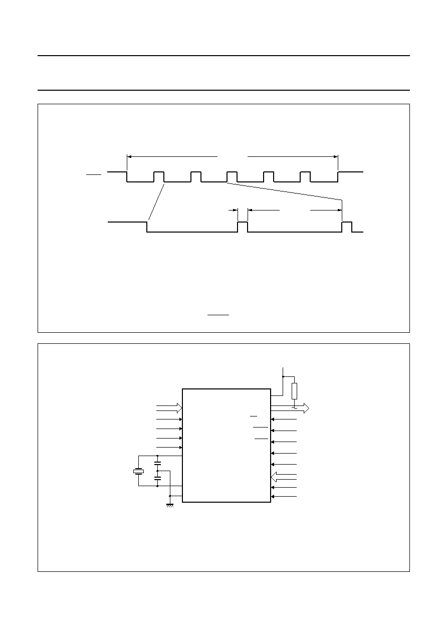
1999 Mar 12
76
Philips Semiconductors
Product specification
8-bit microcontroller
P8xC557E8
Fig.33 PROG waveform.
handbook, full pagewidth
ALE/PROG
5 pulses
50
±
5
µ
s
5
µ
s
MGL170
Fig.34 Program verification P87C557E8.
handbook, full pagewidth
P8xCE560
P1
RST
P3.6
P3.7
XTAL2
4 to 6 MHz
A0 to A7
VSS
XTAL1
VDD
P0
P2.7
P2.6
P2.0 to P2.5
PGM data
A8 to A13
+
5 V
ALE/PROG
PSEN
MBH091
HIGH
HIGH
HIGH
P3.3
LOW
EA/VPP
HIGH
HIGH
LOW
LOW
LOW
P3.4
A14
P3.5
A15
P8xC557E8

1999 Mar 12
77
Philips Semiconductors
Product specification
8-bit microcontroller
P8xC557E8
Table 87 EPROM programming and verification characteristics
V
DD
= 5 V
±
10%; V
SS
= 0 V; T
amb
= 21
∞
C to 27
∞
C.
SYMBOL
PARAMETER
MIN.
MAX.
UNIT
V
PP
programming supply voltage
12.5
13.0
V
I
PP
programming supply current
-
50
mA
f
clk
oscillator frequency
4
6
MHz
t
AVGL
address set-up to PROG LOW
48 t
clk
-
t
GHAX
address hold after PROG HIGH
48 t
clk
-
t
DVGL
data set-up to PROG LOW
48 t
clk
-
t
GHDX
data hold after PROG HIGH
48 t
clk
-
t
EHSH
P2.7 (ENABLE) HIGH to V
pp
48 t
clk
-
t
SHGL
V
pp
set-up to PROG LOW
10
-
µ
s
t
GHSL
V
pp
hold after PROG HIGH
10
-
µ
s
t
GLGH
PROG pulse width
45
55
µ
s
t
AVQV
address to data valid
-
48t
clk
t
ELQV
P2.7 (ENABLE) LOW to data valid
-
48t
clk
t
EHQZ
data float after P2.7 (ENABLE) HIGH
0
48t
clk
t
GHGL
PROG HIGH to PROG LOW
5
-
µ
s
Fig.35 EPROM Programming and Verification.
(1) For programming see Fig.32.
(2) For verification conditions see Fig.34.
handbook, full pagewidth
t GHSL
tGHGL
tGLGH
tSHGL
t AVGL
tDVGL
tGHDX
tGHAX
DATA IN
DATA OUT
ADDRESS
ADDRESS
tAVQV
tEHSH
t ELQV
t EHQZ
HIGH
LOW
P1.0 - P1.7
P2.0 - P2.5
P3.4 - P3.5
PORT 0
ALE/PROG
EA/VPP
MGD633
(ENABLE)
P2.7
PROGRAMMING
(1)
VERIFICATION
(2)
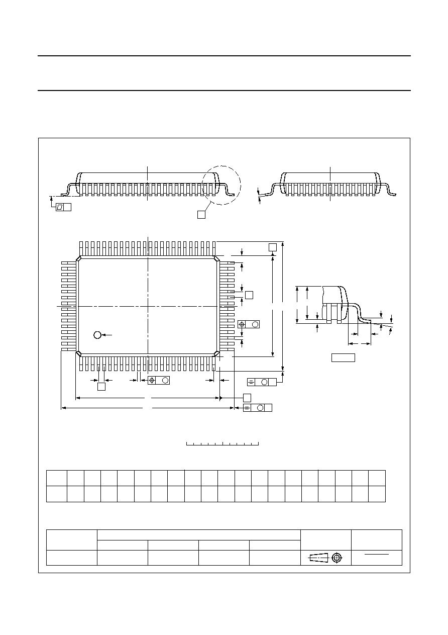
1999 Mar 12
78
Philips Semiconductors
Product specification
8-bit microcontroller
P8xC557E8
24 PACKAGE OUTLINE
UNIT
A
1
A
2
A
3
b
p
c
E
(1)
e
H
E
L
L
p
Z
y
w
v
REFERENCES
OUTLINE
VERSION
EUROPEAN
PROJECTION
ISSUE DATE
IEC
JEDEC
EIAJ
mm
0.36
0.10
2.87
2.57
0.25
0.45
0.30
0.25
0.13
14.1
13.9
0.8
18.2
17.6
1.2
0.8
7
0
o
o
0.2
0.1
0.2
1.95
DIMENSIONS (mm are the original dimensions)
Note
1. Plastic or metal protrusions of 0.25 mm maximum per side are not included.
1.0
0.6
SOT318-1
95-02-04
97-08-01
D
(1)
(1)
(1)
20.1
19.9
H
D
24.2
23.6
E
Z
1.0
0.6
D
b
p
e
E
A
1
A
L
p
detail X
L
(A )
3
B
24
c
b
p
E
H
A
2
D
H
v
M
B
D
Z D
A
Z E
e
v
M
A
1
80
65
64
41
40
25
pin 1 index
X
y
w
M
w
M
0
5
10 mm
scale
80 leads (lead length 1.95 mm); body 14 x 20 x 2.7 mm; high stand-off height
QFP80: plastic quad flat package;
SOT318-1
A
max.
3.3

1999 Mar 12
79
Philips Semiconductors
Product specification
8-bit microcontroller
P8xC557E8
25 SOLDERING
25.1
Introduction
There is no soldering method that is ideal for all IC
packages. Wave soldering is often preferred when
through-hole and surface mounted components are mixed
on one printed-circuit board. However, wave soldering is
not always suitable for surface mounted ICs, or for
printed-circuits with high population densities. In these
situations reflow soldering is often used.
This text gives a very brief insight to a complex technology.
A more in-depth account of soldering ICs can be found in
our
"IC Package Databook" (order code 9398 652 90011).
25.2
Reflow soldering
Reflow soldering techniques are suitable for all QFP
packages.
The choice of heating method may be influenced by larger
plastic QFP packages (44 leads, or more). If infrared or
vapour phase heating is used and the large packages are
not absolutely dry (less than 0.1% moisture content by
weight), vaporization of the small amount of moisture in
them can cause cracking of the plastic body. For more
information, refer to the Drypack chapter in our
"Quality
Reference Handbook" (order code 9397 750 00192).
Reflow soldering requires solder paste (a suspension of
fine solder particles, flux and binding agent) to be applied
to the printed-circuit board by screen printing, stencilling or
pressure-syringe dispensing before package placement.
Several techniques exist for reflowing; for example,
thermal conduction by heated belt. Dwell times vary
between 50 and 300 seconds depending on heating
method. Typical reflow temperatures range from
215 to 250
∞
C.
Preheating is necessary to dry the paste and evaporate
the binding agent. Preheating duration: 45 minutes at
45
∞
C.
25.3
Wave soldering
Wave soldering is not recommended for QFP packages.
This is because of the likelihood of solder bridging due to
closely-spaced leads and the possibility of incomplete
solder penetration in multi-lead devices.
If wave soldering cannot be avoided, the following
conditions must be observed:
∑
A double-wave (a turbulent wave with high upward
pressure followed by a smooth laminar wave)
soldering technique should be used.
∑
The footprint must be at an angle of 45
∞
to the board
direction and must incorporate solder thieves
downstream and at the side corners.
Even with these conditions, do not consider wave
soldering the following packages: QFP52 (SOT379-1),
QFP100 (SOT317-1), QFP100 (SOT317-2),
QFP100 (SOT382-1) or QFP160 (SOT322-1).
During placement and before soldering, the package must
be fixed with a droplet of adhesive. The adhesive can be
applied by screen printing, pin transfer or syringe
dispensing. The package can be soldered after the
adhesive is cured.
Maximum permissible solder temperature is 260
∞
C, and
maximum duration of package immersion in solder is
10 seconds, if cooled to less than 150
∞
C within
6 seconds. Typical dwell time is 4 seconds at 250
∞
C.
A mildly-activated flux will eliminate the need for removal
of corrosive residues in most applications.
25.4
Repairing soldered joints
Fix the component by first soldering two diagonally-
opposite end leads. Use only a low voltage soldering iron
(less than 24 V) applied to the flat part of the lead. Contact
time must be limited to 10 seconds at up to 300
∞
C. When
using a dedicated tool, all other leads can be soldered in
one operation within 2 to 5 seconds between
270 and 320
∞
C.

1999 Mar 12
80
Philips Semiconductors
Product specification
8-bit microcontroller
P8xC557E8
26 DEFINITIONS
27 LIFE SUPPORT APPLICATIONS
These products are not designed for use in life support appliances, devices, or systems where malfunction of these
products can reasonably be expected to result in personal injury. Philips customers using or selling these products for
use in such applications do so at their own risk and agree to fully indemnify Philips for any damages resulting from such
improper use or sale.
28 PURCHASE OF PHILIPS I
2
C COMPONENTS
Data sheet status
Objective specification
This data sheet contains target or goal specifications for product development.
Preliminary specification
This data sheet contains preliminary data; supplementary data may be published later.
Product specification
This data sheet contains final product specifications.
Limiting values
Limiting values given are in accordance with the Absolute Maximum Rating System (IEC 134). Stress above one or
more of the limiting values may cause permanent damage to the device. These are stress ratings only and operation
of the device at these or at any other conditions above those given in the Characteristics sections of the specification
is not implied. Exposure to limiting values for extended periods may affect device reliability.
Application information
Where application information is given, it is advisory and does not form part of the specification.
Purchase of Philips I
2
C components conveys a license under the Philips' I
2
C patent to use the
components in the I
2
C system provided the system conforms to the I
2
C specification defined by
Philips. This specification can be ordered using the code 9398 393 40011.

1999 Mar 12
81
Philips Semiconductors
Product specification
8-bit microcontroller
P8xC557E8
NOTES

1999 Mar 12
82
Philips Semiconductors
Product specification
8-bit microcontroller
P8xC557E8
NOTES

1999 Mar 12
83
Philips Semiconductors
Product specification
8-bit microcontroller
P8xC557E8
NOTES

Internet: http://www.semiconductors.philips.com
Philips Semiconductors ≠ a worldwide company
© Philips Electronics N.V. 1997
SCA55
All rights are reserved. Reproduction in whole or in part is prohibited without the prior written consent of the copyright owner.
The information presented in this document does not form part of any quotation or contract, is believed to be accurate and reliable and may be changed
without notice. No liability will be accepted by the publisher for any consequence of its use. Publication thereof does not convey nor imply any license
under patent- or other industrial or intellectual property rights.
Netherlands: Postbus 90050, 5600 PB EINDHOVEN, Bldg. VB,
Tel. +31 40 27 82785, Fax. +31 40 27 88399
New Zealand: 2 Wagener Place, C.P.O. Box 1041, AUCKLAND,
Tel. +64 9 849 4160, Fax. +64 9 849 7811
Norway: Box 1, Manglerud 0612, OSLO,
Tel. +47 22 74 8000, Fax. +47 22 74 8341
Philippines: Philips Semiconductors Philippines Inc.,
106 Valero St. Salcedo Village, P.O. Box 2108 MCC, MAKATI,
Metro MANILA, Tel. +63 2 816 6380, Fax. +63 2 817 3474
Poland: Ul. Lukiska 10, PL 04-123 WARSZAWA,
Tel. +48 22 612 2831, Fax. +48 22 612 2327
Portugal: see Spain
Romania: see Italy
Russia: Philips Russia, Ul. Usatcheva 35A, 119048 MOSCOW,
Tel. +7 095 755 6918, Fax. +7 095 755 6919
Singapore: Lorong 1, Toa Payoh, SINGAPORE 1231,
Tel. +65 350 2538, Fax. +65 251 6500
Slovakia: see Austria
Slovenia: see Italy
South Africa: S.A. PHILIPS Pty Ltd., 195-215 Main Road Martindale,
2092 JOHANNESBURG, P.O. Box 7430 Johannesburg 2000,
Tel. +27 11 470 5911, Fax. +27 11 470 5494
South America: Rua do Rocio 220, 5th floor, Suite 51,
04552-903 S„o Paulo, S√O PAULO - SP, Brazil,
Tel. +55 11 821 2333, Fax. +55 11 829 1849
Spain: Balmes 22, 08007 BARCELONA,
Tel. +34 3 301 6312, Fax. +34 3 301 4107
Sweden: Kottbygatan 7, Akalla, S-16485 STOCKHOLM,
Tel. +46 8 632 2000, Fax. +46 8 632 2745
Switzerland: Allmendstrasse 140, CH-8027 ZÐRICH,
Tel. +41 1 488 2686, Fax. +41 1 481 7730
Taiwan: Philips Semiconductors, 6F, No. 96, Chien Kuo N. Rd., Sec. 1,
TAIPEI, Taiwan Tel. +886 2 2134 2865, Fax. +886 2 2134 2874
Thailand: PHILIPS ELECTRONICS (THAILAND) Ltd.,
209/2 Sanpavuth-Bangna Road Prakanong, BANGKOK 10260,
Tel. +66 2 745 4090, Fax. +66 2 398 0793
Turkey: Talatpasa Cad. No. 5, 80640 GÐLTEPE/ISTANBUL,
Tel. +90 212 279 2770, Fax. +90 212 282 6707
Ukraine: PHILIPS UKRAINE, 4 Patrice Lumumba str., Building B, Floor 7,
252042 KIEV, Tel. +380 44 264 2776, Fax. +380 44 268 0461
United Kingdom: Philips Semiconductors Ltd., 276 Bath Road, Hayes,
MIDDLESEX UB3 5BX, Tel. +44 181 730 5000, Fax. +44 181 754 8421
United States: 811 East Arques Avenue, SUNNYVALE, CA 94088-3409,
Tel. +1 800 234 7381
Uruguay: see South America
Vietnam: see Singapore
Yugoslavia: PHILIPS, Trg N. Pasica 5/v, 11000 BEOGRAD,
Tel. +381 11 625 344, Fax.+381 11 635 777
For all other countries apply to: Philips Semiconductors, Marketing & Sales Communications,
Building BE-p, P.O. Box 218, 5600 MD EINDHOVEN, The Netherlands, Fax. +31 40 27 24825
Argentina: see South America
Australia: 34 Waterloo Road, NORTH RYDE, NSW 2113,
Tel. +61 2 9805 4455, Fax. +61 2 9805 4466
Austria: Computerstr. 6, A-1101 WIEN, P.O. Box 213, Tel. +43 160 1010,
Fax. +43 160 101 1210
Belarus: Hotel Minsk Business Center, Bld. 3, r. 1211, Volodarski Str. 6,
220050 MINSK, Tel. +375 172 200 733, Fax. +375 172 200 773
Belgium: see The Netherlands
Brazil: see South America
Bulgaria: Philips Bulgaria Ltd., Energoproject, 15th floor,
51 James Bourchier Blvd., 1407 SOFIA,
Tel. +359 2 689 211, Fax. +359 2 689 102
Canada: PHILIPS SEMICONDUCTORS/COMPONENTS,
Tel. +1 800 234 7381
China/Hong Kong: 501 Hong Kong Industrial Technology Centre,
72 Tat Chee Avenue, Kowloon Tong, HONG KONG,
Tel. +852 2319 7888, Fax. +852 2319 7700
Colombia: see South America
Czech Republic: see Austria
Denmark: Prags Boulevard 80, PB 1919, DK-2300 COPENHAGEN S,
Tel. +45 32 88 2636, Fax. +45 31 57 0044
Finland: Sinikalliontie 3, FIN-02630 ESPOO,
Tel. +358 9 615800, Fax. +358 9 61580920
France: 4 Rue du Port-aux-Vins, BP317, 92156 SURESNES Cedex,
Tel. +33 1 40 99 6161, Fax. +33 1 40 99 6427
Germany: Hammerbrookstraþe 69, D-20097 HAMBURG,
Tel. +49 40 23 53 60, Fax. +49 40 23 536 300
Greece: No. 15, 25th March Street, GR 17778 TAVROS/ATHENS,
Tel. +30 1 4894 339/239, Fax. +30 1 4814 240
Hungary: see Austria
India: Philips INDIA Ltd, Band Box Building, 2nd floor,
254-D, Dr. Annie Besant Road, Worli, MUMBAI 400 025,
Tel. +91 22 493 8541, Fax. +91 22 493 0966
Indonesia: see Singapore
Ireland: Newstead, Clonskeagh, DUBLIN 14,
Tel. +353 1 7640 000, Fax. +353 1 7640 200
Israel: RAPAC Electronics, 7 Kehilat Saloniki St, PO Box 18053,
TEL AVIV 61180, Tel. +972 3 645 0444, Fax. +972 3 649 1007
Italy: PHILIPS SEMICONDUCTORS, Piazza IV Novembre 3,
20124 MILANO, Tel. +39 2 6752 2531, Fax. +39 2 6752 2557
Japan: Philips Bldg 13-37, Kohnan 2-chome, Minato-ku, TOKYO 108,
Tel. +81 3 3740 5130, Fax. +81 3 3740 5077
Korea: Philips House, 260-199 Itaewon-dong, Yongsan-ku, SEOUL,
Tel. +82 2 709 1412, Fax. +82 2 709 1415
Malaysia: No. 76 Jalan Universiti, 46200 PETALING JAYA, SELANGOR,
Tel. +60 3 750 5214, Fax. +60 3 757 4880
Mexico: 5900 Gateway East, Suite 200, EL PASO, TEXAS 79905,
Tel. +9-5 800 234 7381
Middle East: see Italy
Printed in The Netherlands
457047/1200/01/pp84
Date of release: 1999 Mar 12
Document order number:
9397 750 02689