
DATA SHEET
Product specification
Supersedes data of 1999 May 17
File under Integrated Circuits, IC20
1999 Jun 11
INTEGRATED CIRCUITS
P8xCx70 family
Microcontrollers for NTSC TVs with
On-Screen Display (OSD) and
Closed Caption (CC)

1999 Jun 11
2
Philips Semiconductors
Product specification
Microcontrollers for NTSC TVs with On-Screen
Display (OSD) and Closed Caption (CC)
P8xCx70 family
CONTENTS
1
FEATURES
2
GENERAL DESCRIPTION
3
ORDERING INFORMATION
4
BLOCK DIAGRAM
5
PINNING INFORMATION
6
MEMORY ORGANIZATION
7
I/O FACILITY
8
WATCHDOG TIMER (T3)
9
REDUCED POWER MODES
10
I
2
C-BUS SERIAL I/O
11
INTERRUPT SYSTEM
12
OSCILLATOR CIRCUITRY
13
RESET
14
PIN FUNCTION SELECTION
15
7-BIT PWM DAC
16
AFT INPUTS (ADC)
17
DATA SLICER AND CC COMMAND
INTERPRETER
18
CC/OSD DISPLAY FUNCTION
19
MEMORY DATA BIT ALLOCATION
20
PROGRAMMER
21
LIMITING VALUES
22
DC CHARACTERISTICS
23
AC CHARACTERISTICS
24
APPLICATION INFORMATION
25
RELEASE LETTER OF ERRATA
26
PACKAGE OUTLINE
27
SOLDERING
28
DEFINITIONS
29
LIFE SUPPORT APPLICATIONS
30
PURCHASE OF PHILIPS I
2
C COMPONENTS

1999 Jun 11
3
Philips Semiconductors
Product specification
Microcontrollers for NTSC TVs with On-Screen
Display (OSD) and Closed Caption (CC)
P8xCx70 family
1
FEATURES
∑
Fully static 80C51 CPU
∑
64-kbyte programmable ROM
∑
1-kbyte RAM
∑
On-chip 12 MHz crystal oscillator
∑
Eight 7-bit PWM outputs for analog controls
∑
Three input 4-bit software Analog-to-Digital Converters
(ADC)
∑
Power-on reset and Watchdog Timer
∑
29 I/O lines via individual addressable controls
∑
Eight port lines (Port 2) with 10 mA LED sink (<1 V)
capability
∑
On-Screen Display (OSD) and Closed Caption (CC)
with V-chip function
∑
Byte-level I
2
C-bus interface up to 400 kHz
∑
Three power reduction modes: Standby, Idle and
Power-down
∑
Power supply: 5.0 V
±
10%
∑
Operating temperature:
-
20 to +70
∞
C
∑
52-pin shrink dual in-line package (SDIP52).
2
GENERAL DESCRIPTION
The P8xCx70 family consists of the following devices:
∑
P83C270
∑
P83C370
∑
P83C570
∑
P83C770
∑
P87C770.
The term P8xCx70 is used throughout this data sheet to
refer to all family members; differences between devices
are highlighted in the text.
The P8xCx70 family of microcontrollers are 8-bit,
80C51-based microcontrollers specifically designed for
the NTSC TV market. Each device has an On-Screen
Display, control functions and Closed Caption that
extracts, decodes (software) and displays caption signals
from NTSC TV signals. Extended Data Service (XDS) is
via the software command interpreter and the V-chip is
also implemented.
3
ORDERING INFORMATION
TYPE NUMBER
PACKAGE
ROM
RAM
NAME
DESCRIPTION
VERSION
P83C270AAR
SDIP52
plastic shrink dual in-line package;
52 leads (600 mil)
SOT247-1
24-kbyte
512-byte
P83C370AAR
32-kbyte
512-byte
P83C570AAR
48-kbyte
1-kbyte
P83C770AAR
64-kbyte
1-kbyte
P87C770AAR
64-kbyte
(OTP)
1-kbyte

1999
Jun
11
4
Philips Semiconductors
Product specification
Microcontrollers for NTSC TVs with On-Screen
Display (OSD) and Closed Caption (CC)
P8xCx70 family
This text is here in white to force landscape pages to be rotated correctly when browsing through the pdf in the Acrobat reader.This text is here in
_
white to force landscape pages to be rotated correctly when browsing through the pdf in the Acrobat reader.This text is here inThis text is here in
white to force landscape pages to be rotated correctly when browsing through the pdf in the Acrobat reader. white to force landscape pages to be ...
4
BLOCK DIAGRAM
b
ook, full pagewidth
MGR380
2
8-bit internal bus
8-BIT
WATCHDOG
TIMER
(T3)
ROM
64-KBYTES
9
◊
7-BIT
DACS
CC DATA SLICER
ON-SCREEN DISPLAY
(OSD)
P2
external
interrupts
8
P0
8
P3
PWM0 to PWM8
(1)
FB
R
G
B
VSYNC
HSYNC
VPP/EA
RESET
ALE/PROG
PSEN
RAM
1-KBYTE
3
◊
4-BIT
ADCS
TWO 16-BIT
TIMER/
COUNTERS
(T0 AND T1)
VSSD
VSSA
VDDP
VDDC
VDDA
FUNCTION
COMBINED
PARALLEL
I/O PORTS
PARALLEL
I/O PORT
CPU
80C51 CORE
EXCLUDING
ROM/RAM
XI
XO
REFH
CVBS
I
2
C-BUS
INTERFACE
SDA
(3)
SCL
(3)
IREF
BLK
STN
8
5
P1
AFT0
(2)
AFT1
(2)
AFT2
(2)
Fig.1 Block diagram.
(1) Alternative functions of Port 0 except PWM0 which is an alternative function of Port 1.
(2) Alternative functions of Port 1.
(3) Alternative functions of Port 3.
1999 Jun 11
5
Philips Semiconductors
Product specification
Microcontrollers for NTSC TVs with On-Screen
Display (OSD) and Closed Caption (CC)
P8xCx70 family
5
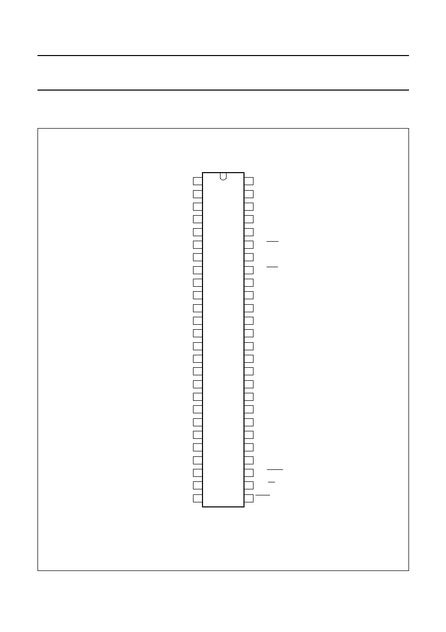
PINNING INFORMATION
5.1
Pinning
Fig.2 Pinning configuration.
handbook, halfpage
P83C270
P83C370
P83C570
P83C770
P87C770
MGR372
1
2
3
4
5
6
7
8
9
10
11
12
13
14
15
16
17
18
19
20
21
22
23
24
25
26
52
51
50
49
48
47
46
45
44
43
42
41
40
39
38
37
36
35
34
33
32
31
30
29
28
27
P0.0/PWM8
P0.1/PWM7
P0.2/PWM6
P0.3/PWM5
P0.4/PWM4
P0.5/PWM3
P0.6/PWM2
P0.7/PWM1
P1.0/AFT0
P1.1/AFT1
P1.2/AFT2
P1.3/PWM0
VSSD
P2.7
P2.6
P2.5
P2.4
P2.3
P2.2
P2.1
P2.0
VSSA
CVBS
STN
BLK
IREF
P3.7
P3.6
P3.5/SDA
P3.4/SCL
P3.3/T1
P3.2/INT0
P3.1/T0
P3.0/INT1
VDDC
RESET
XI
XO
VSSD
VDDP
VDDA
VSYNC
HSYNC
FB
R
G
B
REFH
P1.4
ALE/PROG
VPP/EA
PSEN

1999 Jun 11
6
Philips Semiconductors
Product specification
Microcontrollers for NTSC TVs with On-Screen
Display (OSD) and Closed Caption (CC)
P8xCx70 family
5.2
Pin description
Table 1
SDIP52 package
SYMBOL
PIN
I/O
DESCRIPTION
P0.0/PWM8
to P0.7/PWM1
1 to 8
I/O
Port 0 lines P0.0 to P0.7 (open-drain, bidirectional); alternative functions 7-bit
PWM outputs.
P1.0/AFT0
9
I/O
Port 1 line P1.0; alternative function as 4-bit AFT0 input.
P1.1/AFT1
10
I/O
Port 1 line P1.1; alternative function as 4-bit AFT1 input.
P1.2/AFT2
11
I/O
Port 1 line P1.2; alternative function as 4-bit AFT2 input.
P1.3/PWM0
12
I/O
Port 1 I/O line P1.3 (open-drain, bidirectional); alternative function as 7-bit PWM0
output.
V
SSD
13
-
Ground line for digital circuits.
P2.7 to P2.0
14 to 21
I/O
Port 2 lines P2.7 to P2.0 (open-drain, bidirectional).
V
SSA
22
-
Ground line for analog circuits.
CVBS
23
I
Composite video input.
STN
24
I
Data Slicer decoupling capacitor input, connect to V
SSA
via a 100 nF capacitor.
BLK
25
I
CVBS signal black level reference, connect to V
SSA
via a 100 nF capacitor.
IREF
26
I
CVBS signal reference current input, connect to V
SSA
via a 27 k
resistor.
PSEN
27
O
Program Store Enable (active LOW); bonded out for testing purpose only.
V
PP
/EA
28
I
External Access (active LOW); bonded out for testing purpose only. This pin is also
used for the 12.75 V programming voltage supply in OTP programming modes.
ALE/PROG
29
I/O
Address Latch Enable; bonded out for testing purpose only. This pin is also used
for programming pulses input in OTP programming modes.
P1.4
30
I/O
Port 1 line P1.4 (open-drain, bidirectional).
REFH
31
I
Data Slicer reference high capacitor input, connect to V
SSA
via a 100 nF capacitor.
B
32
O
CC/OSD Blue colour current output.
G
33
O
CC/OSD Green colour current output.
R
34
O
CC/OSD Red colour current output.
FB
35
O
CC/OSD fast blanking output.
HSYNC
36
I
TV horizontal sync input (for OSD synchronization).
VSYNC
37
I
TV vertical sync input (for OSD synchronization).
V
DDA
38
-
+5 V analog power supply.
V
DDP
39
-
+5 V digital power supply for peripherals.
V
SSD
40
I
Ground line for digital circuits.
XO
41
O
System oscillator crystal output.
XI
42
I
System oscillator crystal input.
RESET
43
I
Reset input (active HIGH).
V
DDC
44
-
+5 V digital power supply for CPU core.
P3.0/INT1
45
I/O
Port 3 line P3.0; alternative function as external interrupt 1 input.
P3.1/T0
46
I/O
Port 3 line P3.1; alternative function as Counter 0 input.
P3.2/INT0
47
I/O
Port 3 line P3.2; alternative function as external interrupt 0 input.
P3.3/T1
48
I/O
Port 3 line P3.3; alternative function as Counter 1 input.

1999 Jun 11
7
Philips Semiconductors
Product specification
Microcontrollers for NTSC TVs with On-Screen
Display (OSD) and Closed Caption (CC)
P8xCx70 family
P3.4/SCL
49
I/O
Port 3 line P3.4 (open-drain, bidirectional); alternative function as I
2
C-bus clock
line (open-drain).
P3.5/SDA
50
I/O
Port 3 line P3.5 (open-drain, bidirectional); alternative function as I
2
C-bus data line
(open-drain).
P3.6
51
I/O
Port 3 line P3.6 (open-drain, bidirectional).
P3.7
52
I/O
Port 3 line P3.7 (open-drain, bidirectional).
SYMBOL
PIN
I/O
DESCRIPTION

1999
Jun
11
8
Philips Semiconductors
Product specification
Microcontrollers for NTSC TVs with On-Screen
Display (OSD) and Closed Caption (CC)
P8xCx70 family
6
MEMORY ORGANIZATION
The P8xCx70 family offers a choice of different RAM and ROM configurations; see "Ordering information". The device has no external memory
capability, consequently the RD (read) and WR (write) signals are not bonded out. EA (External Access), PSEN (Program Store Enable) and ALE
(Address Latch Enable) are bonded out for testing purposes only.
For the complete memory map of the P8xC770 family refer to the 80C51 architecture in
"Data Handbook IC20".
6.1
SFR address map summary
The SFRs are presented in ascending address order.
Table 2
SFR address map summary
ADDRESS
REGISTER NAME
7
6
5
4
3
2
1
0
80H
(1)
P0 (latch)
P07
P06
P05
P04
P03
P02
P01
P00
81H
(1)
Stack Pointer (SP)
SP7
SP6
SP5
SP4
SP3
SP2
SP1
SP0
86H
PWM0 (7-bit PWM)
PWM0E data6
data5
data4
data3
data2
data1
data0
87H
(1)
Power Control Register (PCON)
-
-
-
WLE
GF1
GF0
PD
IDL
88H
(1)
Timer/Counter Control Register (TCON)
TF1
TR1
TF0
TR0
IE1
IT1
IE0
IT0
89H
(1)
Timer/Counter Mode Control Register (TMOD)
Gate
C/T
M1
M0
Gate
C/T
M1
M0
8AH
(1)
Timer 0 Low byte (TL0)
TL07
TL06
TL05
TL04
TL03
TL02
TL01
TL00
8BH
(1)
Timer 1 Low byte (TL1)
TL17
TL16
TL15
TL14
TL13
TL12
TL11
TL10
8CH
(1)
Timer 0 High byte (TH0)
TH07
TH06
TH05
TH04
TH03
TH02
TH01
TH00
8DH
(1)
Timer 1 High byte (TH1)
TH17
TH16
TH15
TH14
TH13
TH12
TH11
TH10
90H
(1)
P1 (latch)
P17
P16
P15
P14
P13
P12
P11
P10
92H
Standby Control Register (STBCON)
-
-
-
-
-
-
-
STBY
96H
PWM1 (7-bit PWM)
PWM1E data6
data5
data4
data3
data2
data1
data0
98H
Interrupt Request Register 1 (IRQ1)
-
RCC
RBUSY
-
-
-
-
-
A0H
(1)
P2 (latch)
P27
P26
P25
P24
P23
P22
P21
P20
A6H
PWM2 (7-bit PWM)
PWM2E data6
data5
data4
data3
data2
data1
data0
A8H
(1)
Interrupt Enable Register 0 (IEN0)
EA
-
ES1
-
ET1
EX1
ET0
EX0
B0H
(1)
P3 (latch)
P37
P36
P35
P34
P33
P32
P31
P30
B6H
PWM3 (7-bit PWM)
PWM3E data6
data5
data4
data3
data2
data1
data0
B7H
Slice Line Register (SL)
-
-
-
CS4
CS3
CS2
CS1
CS0
B8H
(1)
Interrupt Priority Register 0 (IP0)
-
-
PS1
-
PT1
PX1
PT0
PX0
C6H
PWM4 (7-bit PWM)
PWM4E data6
data5
data4
data3
data2
data1
data0

1999
Jun
11
9
Philips Semiconductors
Product specification
Microcontrollers for NTSC TVs with On-Screen
Display (OSD) and Closed Caption (CC)
P8xCx70 family
Notes
1. Standard 80C51 registers.
2. Read only registers.
D0H
(1)
Program Status Word (PSW)
CY
AC
F0
RS1
RS0
OV
-
P
D6H
PWM5 (7-bit PWM)
PWM5E data6
data5
data4
data3
data2
data1
data0
D7H
Closed Caption Data 1 (CCData1)
D7
D6
D5
D4
D3
D2
D1
D0
D8H
Serial Control Register (S1CON)
CR2
ENS1
STA
STO
SI
AA
CR1
CR0
D9H
(2)
Status Register (S1STA)
SC4
SC3
SC2
SC1
SC0
0
0
0
DAH
Data Shift Register (S1DAT)
D7
D6
D5
D4
D3
D2
D1
D0
DBH
Slave Address Register (S1ADR)
SLA6
SLA5
SLA4
SLA3
SLA2
SLA1
SLA0
GC
E0H
Accumulator (ACC)
ACC7
ACC6
ACC5
ACC4
ACC3
ACC2
ACC1
ACC0
E6H
PWM6 (7-bit PWM)
PWM6E data6
data5
data4
data3
data2
data1
data0
E7H
Closed Caption Data 2 (CCData2)
D7
D6
D5
D4
D3
D2
D1
D0
E8H
(1)
Interrupt Enable Register 1 (IEN1)
-
ECC
EBUSY
-
-
-
-
-
EAH
AFT Control Register (AFCON)
-
AFTH1
AFTH0
AFTL3
AFTL2
AFTL1
AFTL0
AFTC
EBH
Busy Interrupt and Watchdog Control Register
(BWC)
-
-
-
-
-
-
EW
BUSY
F0H
(1)
B Register (B)
B7
B6
B5
B4
B3
B2
B1
B0
F4H
Port 1 Selection Register (P1SEL)
-
-
-
I
2
CE
-
AFT2E
AFT1E
AFT0E
F5H
PWM8(7-bit PWM)
PWM8E data6
data5
data4
data3
data2
data1
data0
F6H
PWM7(7-bit PWM)
PWM7E data6
data5
data4
data3
data2
data1
data0
F8H
Interrupt Priority Register 1 (IP1)
-
PCC
PBUSY
-
-
-
-
-
FFH
Watchdog Timer Register (WDT)
data7
data6
data5
data4
data3
data2
data1
data0
ADDRESS
REGISTER NAME
7
6
5
4
3
2
1
0

1999 Jun 11
10
Philips Semiconductors
Product specification
Microcontrollers for NTSC TVs with On-Screen
Display (OSD) and Closed Caption (CC)
P8xCx70 family
6.2
Display control registers map
The display control registers can only be addressed using MOVX instructions.
Table 3
Display control register map
ADDRESS
(HEX)
REGISTER NAME
7
6
5
4
3
2
1
0
87F0
Display Control
SRC3
SRC2
SRC1
SRC0
FLF
MSH
MOD1
MOD0
87F1
Text Vertical Position
VPOL
HPOL
VOL5
VOL4
VOL3
VOL2
VOL1
VOL0
87F2
Text Horizontal Position
HOP1
HOP0
TAS5
TAS4
TAS3
TAS2
TAS1
TAS0
87F3
Fringing Control
FRC3
FRC2
FRC1
FRC0
FRDN
FRDE
FRDS
FRDW
87F4
Text Area End
-
-
TAE5
TAE4
TAE3
TAE2
TAE1
TAE0
87F5
Scroll Area
SSH3
SSH2
SSH1
SSH0
SSP3
SSP2
SSP1
SSP0
87F6
Scroll Range
SPS3
SPS2
SPS1
SPS0
STS3
STS2
STS1
STS0
87F7
RGB Brightness
FBPOL
-
-
-
BRI3
BRI2
BRI1
BRI0
87F8
Status (Read)
BUSY
-
FIELD
SCRL
SCR3
SCR2
SCR1
SCR0
Status (Write)
-
H/V
SCON
SCRL
-
-
-
-
87FC
HSYNC Delay
-
HSD6
HSD5
HSD4
HSD3
HSD2
HSD1
HSD0
87FD
Odd/Even Align
-
OEA6
OEA5
OEA4
OEA3
OEA2
OEA1
OEA0
87FE
reserved
-
-
-
-
-
-
-
-
87FF
Configuration
CC
PLUS
ADJ
MIN
-
-
-
-
7
I/O FACILITY
7.1
I/O ports
The P8xCx70 has 29 I/O lines treated as 29 individual
addressable bits or as 4 parallel 8-bit addressable ports,
e.g. Ports 0, 1, 2 and 3, with the exception of Port 1 which
has only 5 lines available.
7.2
Port type
All I/O port pins are open-drain, bidirectional and require
external pull-up resistors. No port options are available for
masking.
Fig.3 Open-drain I/O port.
handbook, halfpage
MGK547
n
Q
from port latch
input data
read port pin
INPUT
BUFFER
I/O pin

1999 Jun 11
11
Philips Semiconductors
Product specification
Microcontrollers for NTSC TVs with On-Screen
Display (OSD) and Closed Caption (CC)
P8xCx70 family
8
WATCHDOG TIMER (T3)
In addition to the standard timers, an 8-bit Watchdog Timer
is also incorporated. When a timer overflow occurs, the
microcontroller is reset. To prevent a system reset the
timer must be reloaded in time by the application software.
If the processor suffers a hardware/software malfunction,
the software will fail to reload the timer. This failure will
result in a reset upon overflow thus preventing the
processor running out of control.
The timer is incremented every 2 ms. The timer interval
between the timer reloading and the occurrence of a reset
depends on the reloaded value. This may range from
2 to 512 ms according to the following formula:
T
timer
256
T3 value
≠
(
)
2 ms
◊
=
The Watchdog Timer can only be reloaded if the condition
flag WLE in SFR PCON has been previously set HIGH by
software. At the moment the counter is loaded WLE is
automatically cleared.
The Watchdog Timer is controlled by the EW bit in SFR
BWC (see Section 11.5). If EW = 1, the Watchdog Timer is
enabled and the Power-down mode disabled. If EW = 0,
the Watchdog Timer is disabled and the Power-down
mode enabled.
In the Idle mode the Watchdog Timer and reset circuitry
remain active.
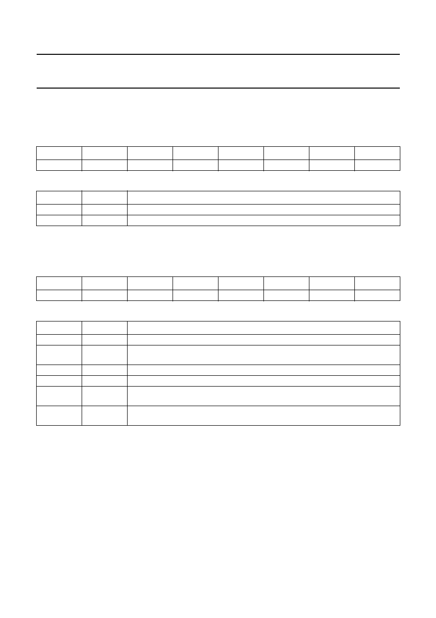
8.1
Watchdog Timer Register (WDT)
Table 4
Watchdog Timer Register (SFR address FFH)
Table 5
Description of the T3 bits
7
6
5
4
3
2
1
0
D7
D6
D5
D4
D3
D2
D1
D0
BIT
SYMBOL
DESCRIPTION
7 to 0
D7 to D0
Watchdog Timer reload value. These 8 bits determine the timer interval. If WDT holds
FFH the timer interval is 2 ms. If WDT holds 00H the timer interval is 512 ms.
handbook, full pagewidth
MGL298
INTERNAL BUS
1/12 fosc
PRESCALER
11-BIT
WDT REGISTER
(8-BIT)
LOAD
CLEAR
LOADEN
write T3
LOADEN
PCON.4
PCON.0
CLEAR
WLE
IDL
internal reset
INTERNAL BUS
RESET
RRESET
Fig.4 Watchdog Timer block diagram.

1999 Jun 11
12
Philips Semiconductors
Product specification
Microcontrollers for NTSC TVs with On-Screen
Display (OSD) and Closed Caption (CC)
P8xCx70 family
9
REDUCED POWER MODES
In order to reduce power consumption three reduced
power modes are available: Standby, Idle and
Power-down.
9.1
Standby mode
In Standby mode full CPU functionality is available but all
analog functions (including the OSD) are disabled.
Power-on reset and the oscillator remain active.
The following also remain active during Standby mode.
∑
CPU
∑
External interrupts INT0 and INT1
∑
T0, T1 and T3
∑
I
2
C-bus interface
∑
PWM outputs.
The Standby mode is entered by setting the STBY bit in
the STBCON register to a logic 1. Recovering from the
Standby mode is achieved by setting the STBY bit back to
a logic 0. After entering the normal mode a waiting time of
10
µ
s has to be taken into account in order to allow the
analog circuitry to stabilize.
9.2
Idle mode
Idle mode operation permits all functions to continue to
work with the exception that the CPU clock is halted.
The following functions remain active during Idle mode:
∑
T0, T1 and T3 (Watchdog Timer)
∑
I
2
C-bus
∑
External interrupts.
9.2.1
E
NTERING
I
DLE MODE
The instruction that sets the IDL bit in the PCON register is
the last instruction executed before entering Idle mode.
Once in the Idle mode the system oscillator keeps running
but the internal clock is gated away from the CPU, but not
gated away from the interrupts, timers and serial port
functions. The CPU status is preserved along with the
Stack Pointer, Program Counter, Program Status Word
and Accumulator. The RAM and all other registers
maintain their data during Idle mode. The port pins retain
the logical states they were holding at Idle mode activation.
9.2.2
R
ECOVERING FROM
I
DLE MODE
There are two methods used to terminate the Idle mode.
Assertion of any enabled interrupt will cause the IDL bit to
be cleared by hardware, thus terminating the Idle mode.
The interrupt is serviced, and following the instruction
RETI, the next instruction to be executed will be the one
following the instruction that put the device into the Idle
mode.
Flag bits GF0 and GF1 may be used to determine whether
the interrupt was received during normal execution or
during Idle mode. For example, the instruction that writes
to the IDL bit can also set or clear one or both flag bits.
When Idle mode is terminated by an interrupt, the service
routine can examine the status of the flag bits.
The second method of terminating the Idle mode is with an
external hardware reset. Since the oscillator is still
running, the hardware reset is required to be active for only
two machine cycles to complete the reset operation. Reset
redefines all SFRs, but does not affect the on-chip RAM.
9.3
Power-down mode
The Power-down operation freezes the oscillator and all
on-chip operations stop. The Power-down mode can only
be entered if the EW bit in SFR BWC is LOW; then the
Power-down mode is entered by setting the PD bit in the
PCON register to a logic 1.
The instruction which sets the PD bit in PCON is the last
instruction executed prior to going into the Power-down
mode. The contents of the on-chip RAM and SFRs are
preserved. The port pins output the values held by their
respective SFRs.
In the Power-down mode V
DD
may be reduced to minimize
power consumption. However, the supply voltage must not
be reduced until Power-down mode is active, and must be
restored before the hardware reset is applied and frees the
oscillator. An on-chip delay counter will count 2048 system
oscillator cycles before enabling the internal clock.
9.3.1
W
AKE
-
UP FROM
P
OWER
-
DOWN USING EXTERNAL
INTERRUPTS
If either of the external interrupts INT0 and INT1 is
switched to level-sensitive and enabled then the interrupt
can be used to wake-up the P8xCx70 from the
Power-down mode. To ensure that the oscillator is stable
before the controller restarts, the internal clock will remain
inactive for 2048 system oscillator cycles.
9.3.2
W
AKE
-
UP FROM
P
OWER
-
DOWN USING
RESET
The Power-down mode can be terminated by holding the
RESET pin HIGH for two machine cycles, this clears the
PD bit. The on-chip delay counter will count 2048 system
oscillator cycles before enabling the internal clock.
1999 Jun 11
13
Philips Semiconductors
Product specification
Microcontrollers for NTSC TVs with On-Screen
Display (OSD) and Closed Caption (CC)
P8xCx70 family
9.4
Control registers
9.4.1
S
TANDBY
C
ONTROL
R
EGISTER
(STBCON)
Table 6
Standby Control Register (SFR address 92H)
Table 7
Description of STBCON bits
9.4.2
P
OWER
C
ONTROL
R
EGISTER
(PCON)
Idle and Power-down modes are activated by software via the Special Function Register PCON.
Table 8
Power Control Register (SFR address 87H)
Table 9
Description of PCON bits
7
6
5
4
3
2
1
0
-
-
-
-
-
-
-
STBY
BIT
SYMBOL
DESCRIPTION
7 to 1
-
These 7-bits are reserved.
0
STBY
Standby mode selection. When STBY = 1, the device enters Standby mode.
7
6
5
4
3
2
1
0
-
-
-
WLE
GF1
GF0
PD
IDL
BIT
SYMBOL
DESCRIPTION
7 to 5
-
These 3 bits are reserved.
4
WLE
Watchdog Load Enable. If WLE = 1, the Watchdog Timer can be loaded. If WLE = 0,
the Watchdog Timer cannot be loaded.
3
GF1
General purpose flag 1.
2
GF0
General purpose flag 0.
1
PD
Power-down mode selection. If PD = 1, the Power-down mode is entered (provided
that the EW bit in SFR BWC is LOW).
0
IDL
Idle mode selection. If IDL = 1, the Idle mode is entered. If IDL = 0, the Idle mode is
inhibited, i.e.normal operation.

1999 Jun 11
14
Philips Semiconductors
Product specification
Microcontrollers for NTSC TVs with On-Screen
Display (OSD) and Closed Caption (CC)
P8xCx70 family
Fig.5 Idle and Power-down circuit.
handbook, full pagewidth
MGL595
OSCILLATOR
CLOCK
GENERATOR
interrupts
serial ports
timer blocks
CC
CPU
IDL
PD
XI
XO
P8xCx70 family

1999 Jun 11
15
Philips Semiconductors
Product specification
Microcontrollers for NTSC TVs with On-Screen
Display (OSD) and Closed Caption (CC)
P8xCx70 family
10 I
2
C-BUS SERIAL I/O
10.1
The I
2
C-bus
This serial port supports the twin line I
2
C-bus. The I
2
C-bus
consists of a serial data line (SDA) and a serial clock line
(SCL). These lines also function as I/O port lines
P3.5 and P3.4 respectively.
The system is unique because data transport, clock
generation, address recognition and bus control arbitration
are all controlled by hardware.
Full details of the I
2
C-bus are given in the document
"The I
2
C-bus and how to use it". This document may be
ordered using the code 9398 393 40011.
10.2
Operation modes
The I
2
C-bus serial I/O has complete autonomy in byte
handling and operates in four modes.
∑
Master transmitter
∑
Master receiver
∑
Slave transmitter
∑
Slave receiver.
These functions are controlled by the S1CON register.
S1STA is the Status Register whose contents may also be
used as a vector to various service routines. S1DAT is the
Data Shift Register and S1ADR the Slave Address
Register. Slave address recognition is performed by
hardware.
Fig.6 Block diagram of the I
2
C-bus serial I/O.
handbook, full pagewidth
MBC749 - 1
SLAVE ADDRESS
S1ADR
GC
SHIFT REGISTER
S1DAT
SDA
ARBITRATION LOGIC
SCL
BUS CLOCK GENERATOR
S1STA
INTERNAL BUS
7
6
5
4
3
2
1
0
S1CON
7
6
5
4
3
2
1
0

1999 Jun 11
16
Philips Semiconductors
Product specification
Microcontrollers for NTSC TVs with On-Screen
Display (OSD) and Closed Caption (CC)
P8xCx70 family
10.3
Serial Control Register (S1CON)
Table 10 Serial Control Register (SFR address D8H)
Table 11 Description of S1CON bits
7
6
5
4
3
2
1
0
CR2
ENS1
STA
STO
SI
AA
CR1
CR0
BIT
SYMBOL
DESCRIPTION
6
ENS1
Enable Serial I/O. When ENS1 = 0, the SIO is disabled and reset. The SDA and SCL
outputs are in a high-impedance state; P3.4 and P3.5 function as open-drain ports.
When ENS1 = 1, the SIO is enabled. The P3.4 and P3.5 port latches must be set to
logic 1.
5
STA
START flag. When the STA bit is set in Slave mode, the SIO hardware checks the
status of the I
2
C-bus and generates a START condition if the bus is free. If STA is set
while the SIO is in Master mode, SIO transmits a repeated START condition.
4
STO
STOP flag. With this bit set while in Master mode a STOP condition is generated. When
a STOP condition is detected on the bus, the SIO hardware clears the STO flag. In the
Slave mode, the STO flag may also be set to recover from an error condition. In this
case, no STOP condition is transmitted to the I
2
C-bus interface. However, the SIO
hardware behaves as if a STOP condition has been received and releases SDA and
SCL. The SIO then switches to the `not addressed' slave receiver mode. The STO flag
is automatically cleared by hardware.
3
SI
SIO interrupt flag. When the SI flag is set, an acknowledge is returned after any one of
the following conditions:
∑
A START condition is generated in Master mode
∑
Own slave address received during AA = 1
∑
General call address received while S1ADR.0 = 1 and AA = 1
∑
Data byte received or transmitted in Master mode (even if arbitration is lost)
∑
Data byte received or transmitted as selected slave
∑
STOP or START condition received as selected slave receiver or transmitter.
2
AA
Assert Acknowledge. When the AA flag is set, an acknowledge (LOW level to SDA)
will be returned during the acknowledge clock pulse on the SCL line when:
∑
Own slave address is received
∑
General call address is received (S1ADR.0 = 1)
∑
Data byte received while device is programmed as a Master receiver
∑
Data byte received while device is a selected Slave receiver.
With AA = 0, no acknowledge will be returned. Consequently, no interrupt is requested
when the `own slave address' or general call address is received.
7
CR2
Clock Rate selection. These three bits determine the serial clock frequency when SIO
is in Master mode; see Table 12. The maximum I
2
C-bus frequency is 400 kHz.
1
CR1
0
CR0
1999 Jun 11
17
Philips Semiconductors
Product specification
Microcontrollers for NTSC TVs with On-Screen
Display (OSD) and Closed Caption (CC)
P8xCx70 family
Table 12 Selection of SCL frequency in Master mode
10.4
Status Register (S1STA)
S1STA is an 8-bit read-only Special Function Register. The contents of S1STA may be used as a vector to a service
routine. This optimizes response time of the software and consequently that of the I
2
C-bus. The status codes for all
possible modes of the I
2
C-bus interface are given in Table 16. The abbreviations used in Table 16 are defined in
Table 15.
Table 13 Status Register (SFR address D9H)
Table 14 Description of S1STA bits
Table 15 Abbreviations used in Table 16
CR2
CR1
CR0
f
osc
DIVISOR
BIT RATE (kHz) at f
osc
= 12 MHz
0
0
0
60
200
0
0
1
1600
7.5
0
1
0
40
300
0
1
1
30
400
1
0
0
240
50
1
0
1
3200
3.75
1
1
0
160
75
1
1
1
120
100
7
6
5
4
3
2
1
0
SC4
SC3
SC2
SC1
SC0
0
0
0
BIT
SYMBOL
DESCRIPTION
7 to 3
SC4 to SC0
5-bit status code; see Table 16.
2 to 0
-
These 3 bits are held LOW.
SYMBOL
DESCRIPTION
SLA
7-bit slave address
R
read bit
W
write bit
ACK
acknowledgment (Acknowledge bit = 0)
ACK
not acknowledge (Acknowledge bit = 1)
DATA
8-bit byte to or from the I
2
C-bus
MST
master
SLV
slave
TRX
transmitter
REC
receiver

1999 Jun 11
18
Philips Semiconductors
Product specification
Microcontrollers for NTSC TVs with On-Screen
Display (OSD) and Closed Caption (CC)
P8xCx70 family
Table 16 Status codes
S1STA VALUE
DESCRIPTION
MST/TRX mode
08H
a START condition has been transmitted
10H
a repeated START condition has been transmitted
18H
SLA and W have been transmitted; ACK received
20H
SLA and W have been transmitted; ACK received
28H
DATA of S1DAT has been transmitted; ACK received
30H
DATA of S1DAT has been transmitted; ACK received
38H
arbitration lost in SLA, R/W or DATA
MST/REC mode
38H
arbitration lost while returning ACK
40H
SLA and R have been transmitted; ACK received
48H
SLA and R have been transmitted; ACK received
50H
DATA has been received; ACK returned
58H
DATA has been received; ACK returned
SLV/REC mode
60H
own SLA and W have been received; ACK returned
68H
arbitration lost in SLA, R/W as MST; own SLA and W have been received; ACK
returned
70H
general CALL has been received; ACK returned
78H
arbitration lost in SLA, R/W as MST; general CALL has been received
80H
previously addressed with own SLA; DATA byte received; ACK returned
88H
previously addressed with own SLA; DATA byte received; ACK returned
90H
previously addressed with general CALL; DATA byte has been received; ACK returned
98H
previously addressed with general CALL; DATA byte has been received; ACK returned
A0H
a STOP condition or repeated START condition has been received while still addressed
as SLV/REC or SLV/TRX
SLV/TRX mode
A8H
own SLA and R have been received. ACK returned
B0H
arbitration lost in SLA, R/W as MST; own SLA and R have been received; ACK returned
B8H
DATA byte has been transmitted; ACK received
C0H
DATA byte has been transmitted; ACK received
C8H
last DATA byte has been transmitted (AA = logic 0) ACK received
Miscellaneous
00H
bus error during MST mode or SLV mode, due to an erroneous START or STOP
condition

1999 Jun 11
19
Philips Semiconductors
Product specification
Microcontrollers for NTSC TVs with On-Screen
Display (OSD) and Closed Caption (CC)
P8xCx70 family
10.5
Data Shift Register (S1DAT)
This register contains the serial data to be transmitted or data has just been received. Bit 7 is transmitted or received first.
Table 17 Data Shift Register (DAH)
10.6
Slave Address Register (S1ADR)
This 8-bit register may be loaded with the 7-bit slave address to which the controller will respond when programmed as
slave receiver/transmitter. The LSB bit (GC) is used to determine whether the general CALL address is recognized.
Table 18 Slave Address Register (SFR address DBH)
Table 19 Description of S1ADR bits
7
6
5
4
3
2
1
0
D7
D6
D5
D4
D3
D2
D1
D0
7
6
5
4
3
2
1
0
SLA6
SLA5
SLA4
SLA3
SLA2
SLA1
SLA0
GC
BIT
SYMBOL
DESCRIPTION
7 to 1
SLA<6-0>
own slave address
0
GC
If GC = 0, the general CALL address is not recognized. If GC = 1, the general CALL
address is recognized.

1999 Jun 11
20
Philips Semiconductors
Product specification
Microcontrollers for NTSC TVs with On-Screen
Display (OSD) and Closed Caption (CC)
P8xCx70 family
11 INTERRUPT SYSTEM
The P8xCx70 has seven interrupt sources, each of which
can be assigned one of two priority levels as shown in
Fig.7. The four interrupt sources common to the 80C51 are
the external interrupts (INT0 and INT1) and the Timer 0
and Timer 1 interrupts. The SIO1 (I
2
C-bus) interrupt is
generated by the S1 flag in the Serial Control Register
(S1CON). This flag is set when SFR S1STA is loaded with
a valid status code. The CC interrupt is generated by the
RCC flag in SFR IRQ1; this flag is set at the end of the
selected CVBS slice line. The BUSY interrupt is generated
by the RBUSY flag which also resides in SFR IRQ1 and is
set by the OSD.
11.1
How interrupts are handled
The interrupt flags are sampled at S5P2 of every machine
cycle. The samples are polled during the following
machine cycle. If one of the flags was in a set condition at
S5P2 of the preceding cycle, the polling cycle will find it
and the interrupt system will generate a LCALL to the
appropriate service routine, provided that LCALL is not
blocked by any of the following conditions:
1. An interrupt of equal priority or higher priority level is
already in progress.
2. The current machine cycle is not the final cycle in the
execution of the instruction in progress (no interrupt
request will be serviced until the instruction in progress
is completed).
3. The instruction in progress is RETI or any access to
the interrupt priority or interrupt enable registers (no
interrupt will be serviced after RETI or after a read or
write to IP0, IP1, IEN0 or IEN1 until at least one other
instruction has been subsequently executed).
The polling cycle is repeated with each machine cycle, and
the values polled are the values that were present at S5P2
of the previous machine cycle. Note that if an interrupt flag
is active but not being responded to for one of the above
mentioned conditions, if the flag is still inactive when the
blocking condition is removed, the denied interrupt will not
be serviced. In other words, the fact that the interrupt flag
was once active but not serviced is not remembered.
Every polling cycle is new.
Note that if an interrupt of higher priority level becomes
active prior to S5P2 of the machine cycle labelled C3, then
in accordance with the rules it will be vectored to during
C5 and C6, without any instruction of the lower priority
routine having been executed. Thus the processor
acknowledges an interrupt request by executing a
hardware generated LCALL to the appropriate servicing
routine. The hardware generated LCALL pushes the
contents of the Program Counter on to the stack (but does
not save the PSW) and reloads the PC with an address
that depends on the source of the interrupt; see Table 20.
Execution proceeds from that location until the RETI
instruction is encountered. The RETI instruction informs
the processor that the interrupt routine is no longer in
progress, then pops the top two bytes from the stack and
reloads the Program Counter. Execution of the interrupted
program continues from where it left off.
Note that a simple RET instruction would also return
execution to the interrupted program, but it would have left
the interrupt control system thinking an interrupt was still in
progress, making future interrupts impossible.
Table 20 Interrupt vectors
Additional details on the interrupt operation are given in
"Data Handbook IC20, 80C51-Based 8-bit
Microcontrollers".
SOURCE
VECTOR ADDRESS
INT0
0003H
I
2
C-bus
002BH
Timer 0
000BH
INT1
0013H
BUSY
0063H
Timer 1
001BH
CC
006BH

1999 Jun 11
21
Philips Semiconductors
Product specification
Microcontrollers for NTSC TVs with On-Screen
Display (OSD) and Closed Caption (CC)
P8xCx70 family
Fig.7 The interrupt structure.
handbook, full pagewidth
INTERRUPT
SOURCES
PRIORITY
GLOBAL
ENABLE
PX0
S1
T0
PX1
BUSY
T1
CC
IEN0/1
REGISTERS
IP0/1
REGISTERS
HIGH
LOW
INTERRUPT POLLING SEQUENCE
MGR378

1999 Jun 11
22
Philips Semiconductors
Product specification
Microcontrollers for NTSC TVs with On-Screen
Display (OSD) and Closed Caption (CC)
P8xCx70 family
11.2
Interrupt enable structure
Each interrupt source can be individually enabled or disabled by setting or clearing its associated bit in the Interrupt
Enable Registers (IEN0 and IEN1). All interrupt sources can also be globally disabled by clearing the EA bit in SFR IEN0.
The Interrupt Enable Registers are described in Sections 11.2.1 and 11.2.2.
11.2.1
I
NTERRUPT
E
NABLE
R
EGISTER
0 (IEN0)
Table 21 Interrupt Enable Register 0 (SFR address A8H)
Table 22 Description of the IEN0 bits
11.2.2
I
NTERRUPT
E
NABLE REGISTER
1 (IEN1)
Table 23 Interrupt Enable Register 1 (SFR address E8H)
Table 24 Description of the IEN1 bits
7
6
5
4
3
2
1
0
EA
-
ES1
-
ET1
EX1
ET0
EX0
BIT
SYMBOL
DESCRIPTION
7
EA
General enable/disable control. When EA = 0, no interrupt is enabled. When EA = 1,
any individually enabled interrupt will be accepted.
6
-
This bit is not used; program to a logic 0 for future compatibility reasons.
5
ES1
Enable I
2
C-bus SIO interrupt.
4
-
This bit is not used; program to a logic 0 for future compatibility reasons.
3
ET1
Enable Timer 1 interrupt.
2
EX1
Enable external interrupt 1.
1
ET0
Enable Timer 0 interrupt.
0
EX0
Enable external interrupt 0.
7
6
5
4
3
2
1
0
-
ECC
EBUSY
-
-
-
-
-
BIT
SYMBOL
DESCRIPTION
7
-
This bit is not used; program to a logic 0 for future compatibility reasons.
6
ECC
Enable external interrupt 8 (CC data ready).
5
EBUSY
Enable external interrupt 7 (BUSY interrupt).
4 to 0
-
These 5 bits are not used; program to logic 0s for future compatibility reasons.

1999 Jun 11
23
Philips Semiconductors
Product specification
Microcontrollers for NTSC TVs with On-Screen
Display (OSD) and Closed Caption (CC)
P8xCx70 family
11.3
Interrupt priority structure
Each interrupt source can be assigned one of two priority
levels. Interrupt priority levels are defined by the Interrupt
Priority Registers (IP0 and IP1). These registers are
described in Sections 11.3.1 and 11.3.2.
A low priority interrupt may be interrupted by a high priority
interrupt level interrupt. A high priority interrupt routine
cannot be interrupted by any other interrupt source. If two
interrupts of different priority occur simultaneously, the
high priority level request is serviced. If requests of the
same priority are received simultaneously, an internal
polling sequence determines which request is serviced.
Thus, within each priority level, there is a second priority
structure determined by the polling sequence. This second
priority structure is shown in Table 25.
Table 25 Interrupt priority
Note
1. The `priority within level' structure is only used to
resolve simultaneous requests of the same priority
level.
SOURCE
PRIORITY WITHIN LEVEL
(1)
INT0
highest
I
2
C-bus
Timer 0
INT1
BUSY
Timer 1
CC
lowest
11.3.1
I
NTERRUPT
P
RIORITY
R
EGISTER
0 (IP0)
Table 26 Interrupt Priority Register 0 (SFR address B8H)
Table 27 Description of IP0 bits
Note
1. Where: logic 0 = low priority; logic 1 = high priority.
7
6
5
4
3
2
1
0
-
-
PS1
-
PT1
PX1
PT0
PX0
BIT
(1)
SYMBOL
DESCRIPTION
7 to 6
-
This bit is not used, program to a logic 0 for future compatibility reasons.
5
PS1
I
2
C-bus SIO interrupt priority level.
4
-
This bit is not used, program to a logic 0 for future compatibility reasons.
3
PT1
Timer 1 interrupt priority level.
2
PX1
External interrupt 1 priority level.
1
PT0
Timer 0 interrupt priority level.
0
PX0
External interrupt 0 priority level.

1999 Jun 11
24
Philips Semiconductors
Product specification
Microcontrollers for NTSC TVs with On-Screen
Display (OSD) and Closed Caption (CC)
P8xCx70 family
11.3.2
I
NTERRUPT
P
RIORITY
R
EGISTER
1 (IP1)
Table 28 Interrupt Priority Register 1 (SFR address F8H)
Table 29 Description of the IP1 bits
11.4
Interrupt Request Register 1 (IRQ1)
An interrupt request from the Closed Caption Data Slicer or from the OSD will be flagged by setting the related bit in the
Interrupt Request Register 1 to a logic 1. These bits must be reset to logic 0s by software.
Table 30 Interrupt Request Register 1 (SFR address 98H)
Table 31 Description of IRQ1 bits
7
6
5
4
3
2
1
0
-
PCC
PBUSY
-
-
-
-
-
BIT
SYMBOL
DESCRIPTION
7
-
This bit is not used, program to a logic 0 for future compatibility reasons.
6
PCC
CC interrupt priority level, fixed to a logic 1.
5
PBUSY
BUSY interrupt 7 priority level, fixed to a logic 1.
4 to 0
-
These 5 bits are not used, program to logic 0s for future compatibility reasons.
7
6
5
4
3
2
1
0
-
RCC
RBUSY
-
-
-
-
-
BIT
SYMBOL
DESCRIPTION
7
-
This bit is not used, program to a logic 0 for future compatibility reasons.
6
RCC
Request for CC interrupt, active HIGH.
5
RBUSY
Request for BUSY interrupt, active HIGH.
4 to 0
-
These 5 bits are not used, program to logic 0s for future compatibility reasons.

1999 Jun 11
25
Philips Semiconductors
Product specification
Microcontrollers for NTSC TVs with On-Screen
Display (OSD) and Closed Caption (CC)
P8xCx70 family
11.5
Busy interrupt and Watchdog Timer control
11.5.1
BUSY
INTERRUPT AND
W
ATCHDOG
C
ONTROL
R
EGISTER
(BWC)
The BUSY signal can generate an interrupt (PX7) to the CPU if enabled by IEN1.5, the vector address is 0063H. This
register is used to enable/disable the BUSY interrupt and the Watchdog Timer.
Table 32 BUSY interrupt and Watchdog Control Register (SFR address EBH)
Table 33 Description of the BWC bits
11.5.2
I
NTERRUPT
R
EQUEST
(RBUSY)
RBUSY is bit 5 of the SFR IRQ1 (address 98H). A falling edge of the active BUSY signal generates a pending interrupt
to the CPU and forces the RBUSY bit HIGH. In the service routine, this bit should be cleared before returning to the main
routine. As long as RBUSY is HIGH, a pending interrupt is always present. Each time BUSY is activated by a falling edge,
the RBUSY is set HIGH. If the interrupt is not served by the next falling BUSY edge, then RBUSY is written to HIGH again
and no error of overrun is indicated.
7
6
5
4
3
2
1
0
-
-
-
-
-
-
EW
BUSY
BIT
SYMBOL
DESCRIPTION
7 to 2
-
These 6 bits are not used.
1
EW
Enable Watchdog Timer. If EW = 0, then the Watchdog Timer is disabled. If EW = 1,
then the Watchdog Timer is enabled and the Power-down mode is disabled.
0
BUSY
When BUSY = 0, an active external interrupt will generate an interrupt to the CPU.
When BUSY = 1, external interrupts are disabled.
It is not recommended to update the display RAM when the BUSY signal is active
(LOW), due to the effect it may have on the OSD display. The display RAM can be
updated when the BUSY signal is inactive.

1999 Jun 11
26
Philips Semiconductors
Product specification
Microcontrollers for NTSC TVs with On-Screen
Display (OSD) and Closed Caption (CC)
P8xCx70 family
12 OSCILLATOR CIRCUITRY
The on-chip oscillator circuitry of the P8xCx70 is a
single-stage inverting amplifier biased by an internal
feedback resistor. For operation as a standard quartz
oscillator or when using an external ceramic resonator,
external components are needed and should be
connected as shown in Fig.8.
In the Power-down mode the oscillator is stopped and both
XI and XO are pulled HIGH. The inverting amplifier and
feedback resistor are both switched off to ensure no
current will flow regardless of the voltages at XI and XO.
To drive the device with an external clock source, apply the
external clock signal to XI, and leave XO to float. There is
no requirement on the duty cycle of the external clock,
because the external clock is divided-by-two using a
flip-flop before feeding the internal clocking circuitry.
The operating frequency of crystal oscillator is fixed at
12 MHz.
13 RESET
There are three ways to invoke a reset and initialize the
P8xCx70:
∑
Via the external RESET pin
∑
Via the on-chip Power-on reset circuitry
∑
Via a Watchdog Timer overflow.
Fig.8 Oscillator configuration.
For quartz crystal or ceramic resonator.
handbook, halfpage
MBE311
XI
XO
The reset mechanism is illustrated in Fig.9. Each reset
source will cause the internal reset signal POC to become
active. The CPU responds by executing an internal reset
putting the internal registers into a defined state as
detailed in Table 34.
13.1
External reset
The reset pin RESET is connected to a Schmitt trigger for
noise reduction (see Fig.9). A reset is accomplished by
holding the RESET pin HIGH for at least 2 machine cycles
(24 system clocks), while the oscillator is running.
If the RESET pin is connected to V
DD
via a capacitor as
shown in Fig.9, an automatic reset can be obtained by
switching on V
DD
, The V
DD
rise time must not exceed
10 ms and the capacitor should be at least 10
µ
F.
The decrease of the RESET pin voltage depends on the
capacitor and the internal resistor R
RESET
. The voltage
must remain above the lower threshold level for a
minimum period determined by the oscillator start-up time
plus 2 machine cycles. For the P8xCx70 an external
capacitor value of 10
µ
F is needed.
13.2
Power-on reset
An on-chip Power-on reset circuit detects supply voltage
variations and generates a Power-on reset pulse
accordingly; see Fig.10.
In the case of supply voltage ramp-up, the power-on reset
signal follows the ramp-up of the supply voltage. When the
trip level (V
t
) is reached, the power-on reset signal will be
maintained for a time period (T
p
) before reverting back to
its LOW state.
In the case of supply voltage drop, after the trip level (V
t
) is
reached, the power-on reset signal will respond within T
r
.
The internal reset will remain active until T
p
after the V
t
has
been exceeded.
The time interval (T
p
) is used to guarantee a complete
power-on reset pulse so that this signal can trigger the
internal reset signal. However, to ensure the oscillator is
stable before the controller starts, the clock is gated away
from the CPU for a further 2048 oscillator cycles.
13.3
Watchdog Timer overflow
The length of the output pulse from T3 is 3 machine cycles.
A pulse of such short duration is necessary in order to
recover from a processor or system fault as fast as
possible.

1999 Jun 11
27
Philips Semiconductors
Product specification
Microcontrollers for NTSC TVs with On-Screen
Display (OSD) and Closed Caption (CC)
P8xCx70 family
Fig.9 On-chip reset configuration.
handbook, full pagewidth
MBK878
SCHMITT
TRIGGER
RESET
CIRCUITRY
overflow Watchdog Timer
Power-on-reset
RSTOUT
10
µ
F
VDD
on-chip circuit
RESET
POC
RRESET
8 k
Fig.10 Power-on reset switching level.
handbook, full pagewidth
MGR379
2048 clocks
START-UP
2048 clocks
Tp
Tp
Supply
voltage
Power-on-
reset
Oscillator
CPU
running
Vt
Vt

1999 Jun 11
28
Philips Semiconductors
Product specification
Microcontrollers for NTSC TVs with On-Screen
Display (OSD) and Closed Caption (CC)
P8xCx70 family
Table 34 The reset value of the SFRs
SFR ADDR
REGISTER
CONTENT
(1)
80H
P0
1111 1111
81H
SP
0000 0111
86H
PWM0
0000 0000
87H
PCON
0000 0000
88H
TCON
0000 0000
89H
TMOD
0000 0000
8AH
TL0
0000 0000
8BH
TL1
0000 0000
8CH
TH0
0000 0000
8DH
TH1
0000 0000
90H
P1
XXX
1 1111
92H
STBCON
XXXX XXX
0
96H
PWM1
0000 0000
98H
IRQ1
X
00
X XXXX
A0H
P2
1111 1111
A6H
PWM2
0000 0000
A8H
IEN0
0000 0000
B0H
P3
1111 1111
B6H
PWM3
0000 0000
B7H
SL
XXX
1 0101
B8H
IP0
XX
0
X
0000
C6H
PWM4
0000 0000
D0H
PSW
0000 0000
D6H
PWM5
0000 0000
D7H
CCData1
0000 0000
Note
1. X = undefined. The internal RAM is not affected by
reset.
D8H
S1CON
X
000 0000
D9H
SISTA
1111 1000
DAH
S1DAT
0000 0000
DBH
S1ADR
0000 0000
E0H
ACC
0000 0000
E6H
PWM6
0000 0000
E7H
CCData2
0000 0000
E8H
IEN1
0110 0000
EAH
AFCON
X000 000X
EBH
BWC
XXXX XX
1
X
F0H
B
0000 0000
F4H
P1SEL
XXX
0
X
000
F5H
PWM8
0000 0000
F6H
PWM7
0000 0000
F8H
IP1
0000 0000
FFH
T3
0000 0000
87F0H
DCR
0000 0000
87F1H
TVPR
0000 0000
87F2H
THPR
0000 0000
87F3H
FCR
0000 0000
87F4H
TAER
0000 0000
87F5H
SSACR
0000 0000
87F6H
SRRR
0000 0000
SFR ADDR
REGISTER
CONTENT
(1)

1999 Jun 11
29
Philips Semiconductors
Product specification
Microcontrollers for NTSC TVs with On-Screen
Display (OSD) and Closed Caption (CC)
P8xCx70 family
14 PIN FUNCTION SELECTION
Ports 0, 1 and 3 are dual purpose ports and can be
configured as port lines or selected as alternative
functions. Selection of the pin as a port line or alternative
function is achieved using the appropriate SFR as
described in Sections 14.1, 14.2.1 and 14.3.
14.1
Port 0 pin function selection
Port 0 is an 8-bit port which can be configured as eight
bidirectional port lines (P0.0 to P0.7) or as eight 7-bit PWM
outputs (PWM1 to PWM8).
Each 7-bit PWM output can be selected by setting the
PWMnE bit in its associated PWMn register to a logic 1
(see Section 15.1). When using these pins as PWM
outputs, the system software needs to keep track of its I/O
status and avoid reading from these ports.
When using these pins as general I/O port lines
(PWMnE = 0), writing is done to the P0 latch and reading
at either the P0 latch or the port pins. No special control is
required for this selection.
14.2
Port 1, P3.4 and P3.5 pin function selection
Port 1 is a 4-bit port which can be configured as four
bidirectional port lines (P1.0 to P1.3) or as three AFT
inputs (AFT0 to AFT2) and one 7-bit PWM output
(PWM0).
The AFT inputs are selected using the Port 1 Selection
Register (P1SEL) as described in Section 14.2.1. This
register also selects the I
2
C-bus functions of P3.4 and
P3.5. The PWM function of the P1.3/PWM0 pin is enabled
by setting the PWM0E bit in SFR PWM0 to a logic 1.
14.2.1
P
ORT
1 S
ELECTION
R
EGISTER
(P1SEL)
Table 35 Port 1 Selection Register (SFR address F4H)
Table 36 Description of P1SEL bits
7
6
5
4
3
2
1
0
-
-
-
I
2
CE
-
AFT2E
AFT1E
AFT0E
BIT
SYMBOL
DESCRIPTION
7
-
These 3 bits are reserved.
6
-
5
-
4
I
2
CE
When I
2
CE = 1, pins 49 and 50 are enabled as alternative functions SCL and SDA
respectively. When I
2
CE = 0, pins 49 and 50 are enabled as general I/O port lines P3.4
and P3.5 respectively.
3
-
This bit is not used.
2
AFT2E
When AFT2E = 1, pin 11 is selected as AFT2 input. When AFT2E = 0, pin 11 is selected
as general I/O port line P1.2.
1
AFT1E
When AFT1E = 1, pin 10 is selected as AFT1 input. When AFT1E = 0, pin 10 is
selected as general I/O port line P1.1.
0
AFT0E
When AFT0E = 1, pin 9 is selected as AFT0 input. When AFT0E = 0, pin 9 is selected
as general I/O port line P1.0.

1999 Jun 11
30
Philips Semiconductors
Product specification
Microcontrollers for NTSC TVs with On-Screen
Display (OSD) and Closed Caption (CC)
P8xCx70 family
14.3
Port 3 pin function selection
Port 3 is an 8-bit port which can be configured as eight bidirectional port lines (P3.0 to P3.7) or as two external interrupts
(INT0 and INT1), two timer/counter inputs (T0 and T1) and the two I
2
C-bus lines (SDA and SCL). Port lines P3.6 and
P3.7 have no alternative functions.
To configure these pins as alternative functions, the corresponding bit in the Port 3 latch (P3) should be programmed to
a logic 1 and the corresponding bit in SFR IEN0 also set to a logic 1.
14.3.1
P
ORT
3 L
ATCH
(P3)
Table 37 Port 3 Latch (SFR address B0H)
Table 38 Description of P3 bits
7
6
5
4
3
2
1
0
P37
P36
P35
P34
P33
P32
P31
P30
BIT
SYMBOL
DESCRIPTION
7
P37
No alternative function available.
6
P36
5
P35
When P35 = 1, pin 50 is used as SDA if the I
2
CE bit in SFR P1SEL is a logic 1.
Otherwise pin 50 is general I/O port line P3.5.
4
P34
When P34 = 1, pin 49 is used as SDL if the I
2
CE bit in SFR P1SEL is a logic 1.
Otherwise pin 49 is general I/O port line P3.4.
3
P33
When P33 = 1, pin 48 is used as Timer 1 input if the ET1 bit in SFR IEN0 is a logic 1.
Otherwise pin 48 is general I/O port line P3.3.
2
P32
When P32 = 1, pin 47 is used as external interrupt INT0 if the EX0 bit in SFR IEN0 is a
logic 1. Otherwise pin 47 is general I/O port line P3.2.
1
P31
When P31 = 1, pin 46 is used as Timer 0 input if the ET0 bit in SFR IEN0 is a logic 1.
Otherwise pin 46 is general I/O port line P3.1.
0
P30
When P30 = 1, pin 45 is used as external interrupt INT1 if the EX1 bit in SFR IEN0 is a
logic 1. Otherwise pin 45 is general I/O port line P3.0.

1999 Jun 11
31
Philips Semiconductors
Product specification
Microcontrollers for NTSC TVs with On-Screen
Display (OSD) and Closed Caption (CC)
P8xCx70 family
15 7-BIT PWM DAC
The P8xCx70 has nine PWM DAC outputs (PWM0 to PWM8) for analog control e.g. volume, balance, bass, treble,
brightness, contrast, sharpness, hue and saturation.
Each PWM output generates a pulse pattern with a repetition rate of
1
/
128
f
PWM
. The analog value is determined by the
ratio of the HIGH-time and the repetition time. A DC voltage proportional to the PWM control setting is obtained by means
of an external integration network (low-pass filter). The polarity of each PWM output is fixed to active HIGH.
The HIGH-time of a PWMn output (within one PWM cycle time) may be calculated as shown in Equation (1).
(1)
Where PWMn is the contents of PWMn data latch; t
0
= 1/f
PWM
and f
PWM
=
1
/
4
f
xtal
.
15.1
SFRs for PWM output control
The alternative PWM functions of Port 0 pins are enabled by writing a logic 1 to the PWMnE bit of the associated Special
Function Register. When setting the PWMnE bit to a logic 0, the associated pin becomes a general I/O port line.
Table 39 SFR data registers for the 7-bit PWMs
REGISTER
ADDRESS
7
6
5
4
3
2
1
0
PWM0
86H
PWM0E
data6
data5
data4
data3
data2
data1
data0
PWM1
96H
PWM1E
data6
data5
data4
data3
data2
data1
data0
PWM2
A6H
PWM2E
data6
data5
data4
data3
data2
data1
data0
PWM3
B6H
PWM3E
data6
data5
data4
data3
data2
data1
data0
PWM4
C6H
PWM4E
data6
data5
data4
data3
data2
data1
data0
PWM5
D6H
PWM5E
data6
data5
data4
data3
data2
data1
data0
PWM6
E6H
PWM6E
data6
data5
data4
data3
data2
data1
data0
PWM7
F6H
PWM7E
data6
data5
data4
data3
data2
data1
data0
PWM8
F5H
PWM8E
data6
data5
data4
data3
data2
data1
data0
t
HIGH
PWMn
t
0
◊
=

1999 Jun 11
32
Philips Semiconductors
Product specification
Microcontrollers for NTSC TVs with On-Screen
Display (OSD) and Closed Caption (CC)
P8xCx70 family
16 AFT INPUTS (ADC)
The P8xCx70 has 3 ADC channels each with 4-bit resolution. One channel is intended to measure the level of the key
pad signals. This is achieved by comparing the AFT signal with the output of a 4-bit DAC.
The compare time of the AFT is not greater than 8
µ
s at 12 MHz. Adding NOP instructions is recommended in between
the instructions which change the reference voltage or channel and the instructions which read the AFTC register bit.
Ensure that pins 9, 10 and 11 are configured as AFT functions before use (see Chapter 14).
The conversion time (T
AFC
) of an AFT (4-bit output) is calculated as shown below.
where:
T
AFC
T
CPU
8
+
(
)
4
µ
s
◊
=
T
CPU
number of instructions to program 4-bit DAC
(
)
instruction cycle time
(
)
◊
=
Fig.11 AFT block diagram.
handbook, full pagewidth
4-BIT DAC
COMPARATOR
AFTL3
AFTL2
AFTL1
AFTL0
AFTH0
AFTH1
AFT2E
AFT1E
AFT0E
MGL596
AFT
CHANNEL
SELECTOR
P1.2/AFT2
P1.1/AFT1
P1.0/AFT0
Vref
EN
DERIVATIVE PORT
SELECTOR
EN1
EN2
AFTC
Internal bus
Internal bus
Channel selection
(SFR address EAH)
EN0
AFT function enable
(SFR address F4H)
(SFR address EAH)
(SFR address EAH)
3

1999 Jun 11
33
Philips Semiconductors
Product specification
Microcontrollers for NTSC TVs with On-Screen
Display (OSD) and Closed Caption (CC)
P8xCx70 family
16.1
AFT Control Register (AFCON)
Table 40 AFT Control Register (SFR address EAH)
Table 41 Description of AFCON bits
Table 42 Selection of AFT channel
7
6
5
4
3
2
1
0
-
AFTH1
AFTH0
AFTL3
AFTL2
AFTL1
AFTL0
AFTC
BIT
SYMBOL
DESCRIPTION
7
-
Reserved.
6
AFTH1
AFT channel selection. These two bits are used to select the AFT channel; see
Table 42.
5
AFTH0
4
AFTL3
AFT reference voltage level selection. These four bits are used to select the analog
output voltage (V
ref
) of the 4-bit DAC. V
ref
is calculated as shown in the equation below:
3
AFTL2
2
AFTL1
1
AFTL0
0
AFTC
AFT compare result. If AFTC = 0; the AFT input voltage is lower than the reference
voltage. If AFTC = 1; the AFC input voltage is higher than the reference voltage.
AFTH1
AFTH0
CHANNEL SELECTED
0
0
AFT0
0
1
AFT1
1
0
AFT2
1
1
illegal code
V
ref
V
DD
16
----------
DAC value
1
+
(
)
◊
=

1999 Jun 11
34
Philips Semiconductors
Product specification
Microcontrollers for NTSC TVs with On-Screen
Display (OSD) and Closed Caption (CC)
P8xCx70 family
17 DATA SLICER AND CC COMMAND INTERPRETER
The P8xCx70 family contains a Data Slicer which slices
Closed Caption data from the CVBS signal. The slice line
is programmable between lines 17 to 23. CC command
interpretation has to be done by a Command Interpreter
which is a relocatable software module. It interprets the
2 bytes that have been sliced off the selected CVBS line
and prepares the display RAM in the OSD block for proper
Closed Caption and OSD display function.
The composite data signal contained within the active
portion of the CVBS line consists of a 7 cycle sine-wave
clock run-in burst, 3 start bits and 16 bits of data. These
16 bits consist of two 8-bit alphanumeric characters
formulated according to the American Standard Code for
Information Interchange (ASCII; x3.4-1967) with odd
parity. The clock rate is 0.5035 MHz which is 32f
h
(horizontal frequency). The clock run-in burst data packet
is 50 IRE units (peak-to-peak). Data is sent with the LSB
(bit D0) being sent first and the MSB (bit D7, the parity bit)
sent last. Figure 13 illustrates CVBS timing.
17.1
Data Slicer
The Composite Video Baseband Signal input should be a
signal which is nominally 1 V
(p-p)
with sync tips negative
and band limited to
±
3% of the standard frequency.
The Data Slicer consists of:
∑
7-bit ADC which converts the analog CVBS signal into
digital data for extraction
∑
Sync separator and bit clock recovery
∑
Data Detector, which extracts the serial stream of bits
from the video signal
∑
Byte Extractor, which performs serial-to-parallel
conversion.
17.1.1
A
NALOG
-
TO
-D
IGITAL
C
ONVERTER
A 7-bit ADC generates a clean CMOS level data signal by
slicing the analog CVBS signal using a 6 MHz clock. The
ADC error is
±
1
/
2
LSB across the full range (2 V
(p-p)
).
17.1.2
S
YNC SEPARATION AND ACQUISITION TIMING
This block contains an acquisition phase-locked loop
which locks onto the incoming video line syncs, with a
frequency error of
±
3% for a varying frequency error and a
wide locking range, such as a VCR.
It also provides a line rate ramp, from which the line based
timing signals for the data detection section may be
decoded.
17.1.3
D
ATA
D
ETECTOR
The data detector consists of a low-pass filter which
screens out signals above 1 MHz (mainly noise); a
DC-loop, which removes DC offset and low frequency
interference and adjusts the slice level continuously; an
amplitude estimator, which provides the DC-loop with an
estimation of signal strength to enable an accurate
adaptive slicing level to be calculated and also aids in the
detection of signal loss or absence of Closed Caption data
and a clock synchronizer, which provides accurate
centre-on-the-incoming data bits clock to the byte
extractor.
17.1.4
B
YTE EXTRACTOR
The Byte extractor extracts data bytes from the sliced bit
stream using the clock provided by the data detector block,
performs serial-to-parallel conversion, then feeds the
2 data bytes to a pair of registers (CCData1 and CCData2)
which hold the 2 data bytes for CC command
interpretation. At the end of the selected CVBS line the
byte extractor will issue the CC interrupt to the CPU. This
interrupt will be generated regardless of whether new data
has been received or not.
17.2
Command Interpreter
The Command Interpreter is implemented in software. It is
used for data field selection, code interpretation and
addressing of the display RAM. It reads the CCData1 and
CCData2 registers, checks for the correct parity, field and
channel number. When the data received is the correct
data, the bytes are passed on to the logic decoder
software that interprets the data and addresses the display
RAM. The CC770 Closed Caption software supports the
three main modes CAPTION, TEXT and XDS. These
operation modes can be selected by the user. For the first
two modes, the data reception will be done in one of two
operating channels C1 or C2 separately for Field 1 or
Field 2 of the video frame. The XDS mode is only available
in Field 2.

1999 Jun 11
35
Philips Semiconductors
Product specification
Microcontrollers for NTSC TVs with On-Screen
Display (OSD) and Closed Caption (CC)
P8xCx70 family
Fig.12 Data Slicer block diagram.
handbook, full pagewidth
MGR278
LEVEL SHIFT
AND ADC
SYNC
SEPARATOR
DATA
DETECTOR
BYTE
EXTRACTOR
CC interrupt
CCData1,
CCData2
BIT CLOCK
RECOVERY
CVBS
Fig.13 Line 21 CVBS Transmission Format.
handbook, full pagewidth
MGK588
50
25
0
20
-
40
-
20
IRE units
Hsync
Program colour burst
clock pulse
in burst
clock run-in
(7 cycles)
Byte 1
Byte 2
Start bit
D0
D6
D0
D6
P
P
Odd/Even
field

1999 Jun 11
36
Philips Semiconductors
Product specification
Microcontrollers for NTSC TVs with On-Screen
Display (OSD) and Closed Caption (CC)
P8xCx70 family
17.3
Closed Caption registers
17.3.1
S
LICE
L
INE
R
EGISTER
(SL)
The Data Slicer contains a software programmable Slice Line Register to extract data from one scan-line out of a range
of scan-lines 17 to 23.
Table 43 Slice Line Register (SFR address B7H)
Table 44 Description of SL bits
17.3.2
C
LOSED
C
APTION
D
ATA
R
EGISTER
1(CCD
ATA
1)
There are two Closed Caption Data Registers: CCData1 and CCData2. At the beginning of the selected CVBS line these
registers will be reset to 00H. The received data will be written into the register at the end of the selected CVBS line, then
also the CC interrupt will be issued. If no data was received, the content of the registers will stay at 00H.
Table 45 Closed Caption Data Register 1 (SFR address D7H)
Table 46 Description of the CCData1 bits
17.3.3
C
LOSED
C
APTION
D
ATA
R
EGISTER
2 (CCD
ATA
2)
Table 47 Closed Caption Data Register 2 (SFR address E7H)
Table 48 Description of CCData2 bits
7
6
5
4
3
2
1
0
-
-
-
CS4
CS3
CS2
CS1
CS0
BIT
SYMBOL
DESCRIPTION
7 to 5
-
These 3 bits are not used.
4 to 0
CS4 to CS0
Scan-line select. These 5 bits are used to select one scan line from scan-lines
17 to 23. For example, the value `10001' selects scan-line 17; the value `10111' selects
scan-line 23.
7
6
5
4
3
2
1
0
D7
D6
D5
D4
D3
D2
D1
D0
BIT
SYMBOL
DESCRIPTION
7 to 0
D7 to D0
Byte 1 as sliced from the selected CVBS line.
7
6
5
4
3
2
1
0
D7
D6
D5
D4
D3
D2
D1
D0
BIT
SYMBOL
DESCRIPTION
7 to 0
D7 to D0
Byte 2 as sliced from the selected CVBS line.

1999 Jun 11
37
Philips Semiconductors
Product specification
Microcontrollers for NTSC TVs with On-Screen
Display (OSD) and Closed Caption (CC)
P8xCx70 family
18 CC/OSD DISPLAY FUNCTION
P8xCx70 contains a display function which covers both
OSD and Closed Caption display requirements.
The design is targeted for the US market. The RGB
outputs are analog signals derived from a DAC together
with the FB (fast blanking) control signal.
18.1
Key features
∑
Fonts
≠ 176 character fonts in masked ROM, each font made
up of a 12
◊
16 ROM matrix
≠ Each character displayed as 12
◊
13 matrix
≠ Special graphic character fonts: maximum
16 characters; each uses masked ROM contents of
2 normal characters; up to 4 different colours can
appear in a character
≠ Character OTP EPROM: 33792 bits (176
◊
12
◊
16).
∑
Display RAM
≠ Display RAM: 560 words of 12 bits/word
≠ Maximum displayed characters: 544.
∑
Screen layout, primary background area:
≠ Vertical range: line 6 of Field 1 (line 269 of Field 2) to
leading edge of VSYNC
≠ Horizontal range: 8
µ
s after trailing edge of HSYNC,
56
µ
s duration
≠ Defines an area with screen colour, large enough that
no adjustment is needed.
∑
Screen layout, CC/OSD text area:
≠ Vertical offset: 0 to 63 scan-lines from trailing edge of
VSYNC
≠ Horizontal offset: 0 to 63 characters from trailing
edge of HSYNC plus 0 to 3 quarters character fine
offset
≠ Maximum CC/OSD rows: 16 (208 scan-lines)
≠ Maximum CC/OSD columns: 48 (12 MHz OSD
clock).
∑
Character and attribute coding, display control modes
≠ Attribute coding is done by combining with character
coding in display RAM
≠ Parallel mode: control display feature on a character
by character basis, i.e. to a character only
≠ Serial mode: apply to a group of characters, valid to
all characters displayed on the same display frame
after set till modified.
∑
Character and attribute coding, `set at' and `set after'
≠ All serial Mode 0 are `set at', i.e., valid from the
character set
≠ Serial Mode 1 at first character position of each row
are `set at'
≠ Serial Mode 1 after first character position are `set
after', i.e. valid from the next character onward.
∑
Colour Look-up Table (CLUT)
≠ Soft colours: 16 entries CLUT; each entry selected
out of 4096 possible colours (4 bits each for R,
G and B)
≠ Primary background screen colour: 16, selected from
CLUT
≠ Foreground colours: 8 + 8, on a parallel
(character-by-character) basis selected from CLUT
≠ Background colours: 16, on a serial (row-by-row)
basis selected from CLUT.
∑
Display character size
≠ Horizontal display size: 1
◊
or 2
◊
OSD clock periods
per dot, on a serial basis
≠ Vertical display size: 1
◊
or 2
◊
scan-lines per dot, on a
serial basis.
∑
Special attributes
≠ Flash, Italic, Underline, Overline attributes via
attribute coding on a serial basis, Mode 0 `set at'
≠ Proportional spacing supported
≠ Fringing (shadowing): independent north, south, east
and/or west fringing on a screen (applied to all
characters displayed) basis via a control register
≠ Boxing attribute via attribute coding on a serial basis,
both Mode 0 and Mode 1 possible
≠ Meshing attribute on a screen basis via control
register; background colour areas are modified to
display background colours and video alternately,
provided in Mixed Video display mode
≠ Flashing (blinking) on a serial basis, Mode 0 `set at';
flashing frequency: 50% duty, 1 or 2 Hz, done via a
control register.

1999 Jun 11
38
Philips Semiconductors
Product specification
Microcontrollers for NTSC TVs with On-Screen
Display (OSD) and Closed Caption (CC)
P8xCx70 family
∑
Automatic soft scroll
≠ Programmable soft scroll display area height up to
16 rows
≠ Programmable soft scroll display area top row
≠ Programmable row range for soft scroll
≠ Scroll map maintained in display RAM; number of
entries equals scroll display area height, up to
16 entries; display RAM positions occupied not
usable for coding display characters.
∑
Miscellaneous
≠ Programmable HSYNC and VSYNC active polarity
≠ Programmable FBL (fast blanking) and R, G and B
(during line fly-back periods) polarity
≠ 16 level RGB brightness control
≠ Video, Full Text, Mixed Screen Colour, Mixed Video
display modes.
18.2
Display features
18.2.1
F
LASH
This attribute is valid from the time set until end of row or
otherwise modified.
Flashing causes the foreground colour pixels to be
displayed as background pixels. This means that the
fringing, if set, will only be visible when the foreground
colour pixels are displayed as foreground colour. The flash
frequency can be set to either 1 or 2 Hz (see
Section 18.4.5).
18.2.2
F
RINGING
This attribute is valid from the time set until end of row or
otherwise modified.
Fringing causes an edge (fringe) to be put around the
foreground pixels. Fringing is an attribute that can be
applied to characters providing a shadow around the
shape of the foreground information. The fringe is 1 line
wide in the vertical direction and 1 pixel wide in the
horizontal direction. Fringing applies to all characters
except those in columns 8 and 9.
The size of the fringe is independent of the size attributes
and always remains 1 scan-line vertically and 1 pixel
horizontally for even and odd field.
Fringing is only effective within the text area and will not
extend over the text area borders. Fringing will cross the
borders of boxes in the horizontal direction, but will not
cross between rows in the vertical direction. Special
facilities are provided for combined characters (see
Section 18.10).
18.2.3
S
IZE
Two sizes are offered in both horizontal and vertical
directions. The sizes available are normal, double
height/width and any combinations of these. The attribute
settings are always valid for a whole row. Mixing of sizes
within a row is not possible. The first character in the row
must be the serial attribute, Mode 1 if the default of normal
size is to be overridden. These attributes will be ignored in
any other position. For additional details see
Section 18.3.2.
18.2.4
I
TALICS
This attribute is valid from the time set until end of row or
otherwise modified
.
This attribute causes the character
foreground pixels to be offset horizontally by 1 pixel per
4 scan-lines (interlaced mode); see Fig.14.
The base is the bottom left character matrix pixel.
The pattern of the character will be indented 1 pixel every
2 scan-lines per field, starting from the base of the
character. Fringing is shifted accordingly.
18.2.5
P
ROPORTIONAL SPACING
The character font ROM in column A, contains the
half-width characters: f, i, j, l and t. These characters have
a width of only 6 pixels instead of the normal 12. Examples
of half-width characters are shown in Fig.15.
If some of the characters are not used for depicting narrow
characters they may be used as normal. In this case they
are accessible via column D (see Fig.27).

1999 Jun 11
39
Philips Semiconductors
Product specification
Microcontrollers for NTSC TVs with On-Screen
Display (OSD) and Closed Caption (CC)
P8xCx70 family
Fig.14 Italics.
handbook, full pagewidth
0
0
1
3
5
7
8
9
10
field 1
indented by 6
indented by 5
indented by 4
indented by 3
indented by 2
indented by 1
not indented
MGL146
field 2
11
12
2
2
4
4
6
6
8
10
0
2
4
6
8
10
Fig.15 Proportional spacing.
handbook, full pagewidth
MGL147

1999 Jun 11
40
Philips Semiconductors
Product specification
Microcontrollers for NTSC TVs with On-Screen
Display (OSD) and Closed Caption (CC)
P8xCx70 family
18.2.6
C
OLOUR
L
OOK
-
UP
T
ABLE
(CLUT)
A Colour Look-up Table with 16 colours is provided. The colours are programmable from a palette of 4096 (4 bits per R,
G and B). The CLUT is defined by writing data to the RAM as described in Section 18.6.
Table 49 CLUT colour values
18.2.7
F
AST
B
LANKING POLARITY
The polarity of the Fast Blanking signal (FBL) can be inverted. When inverted the values of the RGB outputs during line
fly-back periods are also inverted. The polarity is set using the FBPOL bit in the RGB Brightness Register (see
Section 18.9.8).
Table 50 RGB blanking interval values
Table 51 Fast Blanking signal polarity
18.2.8
RGB B
RIGHTNESS
C
ONTROL
A brightness control is provided that allows the RGB output voltages to be modified. The brightness is set using the
BRI0 to BRI3 bits in the RGB Brightness Register (see Section 18.9.8).
Table 52 RGB brightness selection
RED<3-0>
GREEN<3-0>
BLUE<3-0>
COLOUR VALUE
11
10
9
8
7
6
5
4
3
2
1
0
0
0
0
0
0
0
0
0
0
0
0
0
lowest value
1
1
1
1
1
1
1
1
1
1
1
1
highest value
FBOL
RED<3-0>
GREEN<3-0>
BLUE<3-0>
CONDITIONS
11
10
9
8
7
6
5
4
3
2
1
0
0
0
0
0
0
0
0
0
0
0
0
0
0
Normal operation
1
1
1
1
1
1
1
1
1
1
1
1
1
Inverted Fast
Blanking signal
FBPOL
FBL
CONDITION
0
1
RGB display
0
0
Video display
1
0
RGB display
1
1
Video display
BRI3
BRI2
BRI1
BRI0
RGB BRIGHTNESS
0
0
0
0
lowest value
1
1
1
1
highest value

1999 Jun 11
41
Philips Semiconductors
Product specification
Microcontrollers for NTSC TVs with On-Screen
Display (OSD) and Closed Caption (CC)
P8xCx70 family
18.2.9
F
OREGROUND COLOUR
The foreground colour can be chosen from 8 colours on a
character-by-character basis. Two sets of 8 colours are
provided. A serial attribute switches between the banks
(see Serial Mode 1, bit 7). The colours are the CLUT
entries 0 to 7 or 8 to 15.
18.2.10 B
ACKGROUND COLOUR
This attribute is valid from the time set until end of row or
otherwise modified if set with Serial Mode 0. If set with
Serial Mode 1, then the colour is set from the next
character onwards (see Section 18.3.2).
The background colour can be chosen from all 16 CLUT
entries.
18.2.11 B
OXES
This attribute is valid from the time set until end of row or
otherwise modified if set with Serial Mode 0. If set with
Serial Mode 1, then it is set from the next character
onwards (see Section 18.3.2).
In text mode the background colour is displayed
regardless of the setting of the box attribute bit. Boxes take
affect only during mixed mode, where boxes are set in this
mode the background colour is displayed. Character
locations where boxes are not set show video/screen
colour (depending on the setting in the Display Control
Register) instead of the background colour.
18.2.12 M
ESHING
Meshing effects the background colour:
∑
In text mode all background colour will be meshed
∑
During mixed modes the background colour will only be
displayed where boxes are active, therefore meshing
will only be displayed inside these areas.
The appearance of the background colour is modified by
the meshing control bit (MSH). If meshing is set then the
background pixels, where displayed, are alternately
displayed at pixel rate in the background colour and as
video/screen colour, depending on which of the mixed
modes is set. The structure is offset by 1 pixel from
scan-line to scan-line, thus achieving a checker board
display of the background colour.
Meshing is set in the Display Control Register, see
Section 18.9.1.
18.2.13 B
ACKGROUND DURATION
The background duration attribute can be set with the
Serial Mode 1 attribute, see Section 18.3.2.
In combination with the End Of Row attribute (see
Section 18.2.17), it forces the background colour to be
displayed on the row until the end of the text area is
reached.
When set, this attribute takes effect from the current
position until the end of the text display as defined in the
Text Area End Register (see Section 18.9.5).
18.2.14 U
NDERLINE
This attribute is valid from the time set until end of row or
otherwise modified if set with Serial Mode 0. If set with
Serial Mode 1, then it is set from the next character
onwards (see Section 18.3.2).
The underline attribute causes the characters to have the
bottom scan-line of the character cell forced to foreground
colour, including spaces. If background duration is set,
then underline is set until the end of the text area.
18.2.15 O
VERLINE
This attribute is valid from the time set until end of row or
otherwise modified if set with Serial Mode 0. If set with
Serial Mode 1, then it is set from the next character
onwards (see Section 18.3.2).
The overline attribute causes the characters to have the
top scan-line of the character cell forced to foreground
colour, including spaces. If background duration is set,
then overline is set until the end of the text area.
18.2.16 S
PECIAL GRAPHIC CHARACTERS
Several special characters are provided for special effects.
These characters provide a choice of 4 colours within a
character cell. The number of characters is limited to 16.
Characters are stored in columns 8 and 9 of the ROM
table (32 ROM characters). Each character uses the ROM
contents of 2 normal characters. Addressing is therefore
done using only the even character addresses. The pixel
planes are stored in adjacent character locations, always
starting with an even character. The pixel plane 0 is stored
in the even character and pixel plane 1 is stored in the odd
character ROM position
There is no fringing possible for these characters.
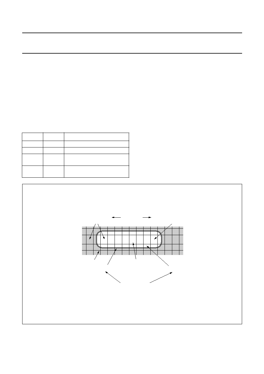
1999 Jun 11
42
Philips Semiconductors
Product specification
Microcontrollers for NTSC TVs with On-Screen
Display (OSD) and Closed Caption (CC)
P8xCx70 family
If some of the characters are not used for depicting special
characters they may be used as normal. In this case they
are accessible via the columns B and C
(see Section 18.10).
The four colours are allocated as shown in Table 53.
An example of a special character is shown in Fig.16. If the
screen colour is transparent (implicit in Mixed mode) and
inside the object the box attribute is set, then the object is
surrounded by video. If the box attribute is not set the
background colour inside the object will also be displayed
as transparent.
Table 53 Special character colours
PLANE1
PLANE0
COLOUR ALLOCATION
0
0
background colour
0
1
foreground colour
1
0
foreground colour 6 or 14
depending on the set bank
1
1
foreground colour 7 or 15
depending on the set bank
18.2.17 E
ND OF
R
OW
The number of characters in a row is flexible and can be
determined by the end of row bit in the Serial Mode 1
character attribute, however the maximum number of
characters is determined by the setting of the text area
start and the text area end register.
The total number of characters displayed on a page is
limited by the internal RAM size. The characters are stored
sequential in the memory.
Fig.16 Special character example.
handbook, full pagewidth
MGK550
VOLUME
background colour
"set at" (Mode 0)
background colour
"set after" (Mode 1)
serial attribute
foreground colour 7
background colour
special character
foreground colour
normal character
foreground colour 6

1999 Jun 11
43
Philips Semiconductors
Product specification
Microcontrollers for NTSC TVs with On-Screen
Display (OSD) and Closed Caption (CC)
P8xCx70 family
18.3
Character and attribute coding
Character coding is split into character oriented attributes
(parallel) and character group coding (serial). The serial
attributes take effect at the set position and remain
effective until either modified by new serial attributes or
until the end of the row. A serial attribute is represented as
a space (the space character itself however is not used for
this purpose). The attributes are still active, e.g. overline
and underline will be visible.
The default settings at the start of a row are:
∑
Foreground colour = 0, foreground colour switch = 0
(bank 0)
∑
Background colour = 8
∑
1x size
∑
Flash off
∑
Overline off
∑
Underline off
∑
Italics off
∑
Display mode = superimpose
∑
Fringing off
∑
Background colour duration = 0
∑
End of Row = 0.
The coding is done in 12-bit words. The codes are stored
sequentially in the display memory.
18.3.1
P
ARALLEL CHARACTER CODING
Table 54 Parallel character coding
18.3.2
S
ERIAL CHARACTER CODING
Table 55 Serial character coding
BITS
DESCRIPTION
0 to 7
8-bit character code
8 to 10
3 bits for 8 foreground colours
11
Mode bit: a logic 0 = parallel code
BITS
SERIAL MODE 0 (`SET AT')
SERIAL MODE 1
CHAR. POSITION = 1 (`SET AT') CHAR. POSITION >1 (`SET AFTER')
0 to 3
4 bits for 16 background colours 4 bits for 16 background colours
4 bits for 16 background colours
4
0 = Underline off
1 = Underline on
Horizontal Size:
0 = normal; 1 = x2
0 = Underline off
1 = Underline on
5
0 = Overline off
1 = Overline on
Vertical Size:
0 = normal; 1 = x2
0 = Overline off
1 = Overline on
6
Display mode:
0 = Superimpose; 1 = Boxing
Display mode:
0 = Superimpose; 1 = Boxing
Display mode:
0 = Superimpose; 1 = Boxing
7
0 = Flash off
1 = Flash on
Foreground colour switch
0 = Bank 0 (colours 0 to 7)
1 = Bank 1 (colours 8 to 15)
Foreground colour switch
0 = Bank 0 (colours 0 to 7)
1 = Bank 1 (colours 8 to 15)
8
0 = Italics off
1 = Italics on
Background colour duration:
0 = stop BGC
1 = set BGC to end of row
Background colour duration (set at):
0 = stop BGC
1 = set BGC to end of row
9
0 = Fringing off
1 = Fringing on
End of Row
0 = Continue Row; 1 = End Row
End of Row (set at):
0 = Continue Row; 1 = End Row
10
Switch for Serial coding
Mode 0 and 1: 0 = Mode 0
Switch for Serial coding
Mode 0 and 1: 1 = Mode 1
Switch for Serial coding
Mode 0 and 1: 1 = Mode 1
11
Mode bit: 1 = Serial code
Mode bit: 1 = Serial code
Mode bit: 1 = Serial code

1999 Jun 11
44
Philips Semiconductors
Product specification
Microcontrollers for NTSC TVs with On-Screen
Display (OSD) and Closed Caption (CC)
P8xCx70 family
18.4
Screen controls
A number of 8-bit registers are provided which are used to
select various parameters for the whole screen.
18.4.1
D
ISPLAY MODES
When superimpose or boxing are set, the resulting display
depends on the setting of the screen display mode bits.
The mode is selected by the MOD0 and MOD1 bits of the
Display Control Register (see Section 18.9.1).
∑
Video mode: disables all display activities and sets the
RGB to true black and FBL to video.
∑
Full Text mode: displays screen colour at all locations
not covered by character foreground or background
colour. The box attribute has no effect.
∑
Mixed Screen mode: displays screen colour at all
locations not covered by character foreground or, within
boxed areas, background colour.
∑
Mixed Video mode: displays video at all locations not
covered by character foreground or within boxed areas,
background colour.
Table 56 Selection of screen display modes
18.4.2
F
RINGING CONTROLS
18.4.2.1
Fringing direction
Fringing can be set to work in any direction (N, S, E and
W). The direction is selected by setting one of the four
FRDx bits in the Fringing Control Register (see
Section 18.9.4). Where x = N, S, E or W and N = North,
S = South etc.
Table 57 Selection of Fringing direction
MOD1
MOD0
DISPLAY MODE
0
0
Video mode
0
1
Full Text mode
1
0
Mixed Screen mode
1
1
Mixed Video mode
FRDx
FRINGING DIRECTION
0
off
1
on
18.4.3
F
RINGING COLOUR
The colour of the fringe is set by the FRC0 to FRC3 bits in
the Fringing Control Register (see Section 18.9.4).
Any one of 16 colours can be selected.
Table 58 Fringing colour
18.4.4
S
CREEN COLOUR
The screen colour can be any one of 16 colours.The colour
is selected using the SRC0 to SRC3 bits in the Display
Control Register (see Section 18.9.1).The screen colour
covers the full video width, as described in Section 18.7.1.
It is visible when the Text mode is set and no foreground
or background pixels are being displayed (see
Section 18.4.1).
Table 59 Selection of the screen colour
18.4.5
F
LASH FREQUENCY
The flash frequency is set by the FLF bit in the Display
Control Register; (see Section 18.9.1).
Table 60 Selection of the flash frequency
FRC<3-0>
FRINGING COLOUR
3
2
1
0
0
0
0
0
Colour 0
1
1
1
1
Colour 15
SRC<3-0>
SCREEN COLOUR
3
2
1
0
0
0
0
0
Colour 0
1
1
1
1
Colour 15
FLF
FLASH FREQUENCY
0
approximately 1 Hz with a 50% active ratio
1
approximately 2 Hz with a 50% active ratio

1999 Jun 11
45
Philips Semiconductors
Product specification
Microcontrollers for NTSC TVs with On-Screen
Display (OSD) and Closed Caption (CC)
P8xCx70 family
18.5
Text display controls
These controls are used for defining the display areas.
Two types of areas are possible. One area is static and
controlled via the main row counter, while the other is
dynamic and can be soft scrolled. The areas cannot cross
each other. Only one soft scroll area is possible.
A scroll map is provided which is addressed by the display
row and contains the address of the data in the memory
that is to be displayed. A bit is also provided to enable the
text display, outside of the scroll area.
Outside the defined scroll area, the scroll map is
addressed by the main row counter. Within the visible soft
scroll area, the scroll map is addressed by the scroll row
counter. The text display enable bit within this area is
ignored.
The number of rows that can be scrolled through can be
set by defining the start row (scroll map value) and end
row. The defined number of rows should be at least one
more than the visible scroll area height.
The height of the visible area is defined as a number of
rows. The position of the scroll area is defined as an offset
in number of rows from the start of the text area.
The values programmed into the registers must ensure a
sensible display. the following should be noted:
∑
If values are programmed that cause the display to go
beyond the vertical sync signal, the display will stop and
react as if finished
∑
If the visible scroll area is made larger than the number
of rows allocated to the scroll function, then they will
wrap around and be repeated
∑
If the defined range of rows for scrolling is greater than
the scroll area, these rows should not be used for other
display purposes.
18.5.1
S
OFT SCROLL ACTION
The soft scrolling function is done by modifying the start
count of the row scan-line count of the first scroll row. This
is decremented once per frame automatically thus
providing the effect of the top row disappearing while the
bottom row is appearing.
At the count 0, the scroll row counter is incremented
automatically and the line-scan counter is set to 12 again.
This pushes the top row to the bottom. This row must be
cleared by the core during the fly-back period.
If the number of rows allocated to the scroll counter is
larger than the defined visible scroll area, this allows parts
of rows at the top and bottom to be displayed during the
scroll function.
Only screens which contain single height rows or only
double height rows can be scrolled.
18.5.1.1
Soft scroll enable
The soft scroll function is started by writing a logic 1 to the
SCRL bit in the Read Only Status Register (see
Section 18.9.9). This bit will be cleared when the scrolling
of one row is completed.
A hard scrolling action can also be performed when writing
a logic 0 to the SCRL bit in the Write Only Status Register.
If a logic 0 is written to this bit, the display in the scroll area
is subsequently shifted up by one row.
Table 61 Soft scroll enable
18.5.1.2
Soft scroll area enable
The SCON bit in the Status Register controls whether a
scroll area is active or not. The default value is no scroll
area enabled, and the display is controlled only by the
scroll map entries. When this bit is set to a logic 1 the scroll
area is activated and the values contained in the SSACR,
SRRR and STA registers take effect.
Table 62 Soft scroll area enable
SCRL
SOFT SCROLL
0
Activates hard scroll, shifts display in one
row increment, stops soft scroll.
1
Start scrolling function.
SCON
SOFT SCROLL AREA
0
no scroll area enabled
1
scroll area enabled

1999 Jun 11
46
Philips Semiconductors
Product specification
Microcontrollers for NTSC TVs with On-Screen
Display (OSD) and Closed Caption (CC)
P8xCx70 family
18.5.1.3
Top display row select
The top display row of the scroll area is set using the
SSP0 to SSP3 bits in the Soft Scroll Area Control Register
(see Section 18.9.6).
Table 63 Soft scroll area position value
18.5.1.4
Visible scroll area height selection
The visible scroll area height is set using the
SSH0 to SSH3 bits in the Soft Scroll Area Control Register
(see Section 18.9.6).
Table 64 Soft scroll area height value
SSP<3-0>
DISPLAY AREA POSITION
3
2
1
0
0
0
0
0
Row 0
1
1
1
1
Row 15
SSH<3-0>
DISPLAY AREA HEIGHT
3
2
1
0
0
0
0
0
1 Row
1
1
1
1
16 Rows
18.5.1.5
Scroll rows range selection
The scroll rows range is set in the Scroll Rows Range
Register (see Section 18.9.7). Setting this register
initialises the scroll row counter so that the first (top) row is
the Start Scroll Row Number. By redefining the contents of
this register a hard scrolling can also be achieved. If a new
start scroll row number is loaded during a soft scroll action,
then this value will be taken as the new start value after the
scrolling action has been completed.
Table 65 Start scroll row number
Table 66 Stop scroll row number
STS<3-0>
START SCROLL ROW
NUMBER
3
2
1
0
0
0
0
0
Row 0
1
1
1
1
Row 15
SPS<3-0>
STOP SCROLL ROW
NUMBER
3
2
1
0
0
0
0
0
Row 0
1
1
1
1
Row 15
Fig.17 Soft scroll area.
handbook, full pagewidth
15
MGL148
14
13
12
11
10
9
8
7
6
5
scroll area position
pointer
(SSP3 to SSP0 e.g. 6)
visible area height
(SSH3 to SSH0 e.g. 4)
4
3
2
1
0
ROW
usable for OSD display
usable for OSD display
should not be used for
OSD display
should not be used for
OSD display
soft scrolling area
start row (STR3 to STR0 e.g. 3)
stop row (SPR3 to SPR0 e.g. 11)

1999 Jun 11
47
Philips Semiconductors
Product specification
Microcontrollers for NTSC TVs with On-Screen
Display (OSD) and Closed Caption (CC)
P8xCx70 family
18.5.2
S
CROLL MAP
The scroll map allows a flexible allocation of data in the memory, to individual rows. Sixteen 12-bit words are provided in
the display memory for this purpose. The bit allocation is shown in Table 67. The scroll map memory is located in the
first 16 words in the display memory (data byte addresses 8000H to 801FH) as shown in Fig.18.
Table 67 Scroll map word format
BIT
DESCRIPTION
11
Text display enable, valid outside soft scroll area. A logic 0 = disable; a logic 1 = enable.
10
Reserved, should be set to a logic 0.
9 to 0
Pointer to row data.
Fig.18 Scroll map and data pointers.
handbook, full pagewidth
MGK549
0
1
2
3
4
5
6
7
8
9
10
11
12
13
14
15
0
1
2
3
4
Row counter
0 to 15 valid
10
11
Scroll counter
3 to 11 valid
3
4
9
10
11
Row counter
0 to 15 valid
12
13
14
15
,,,
,,,
,,,
,,,
,,,
,,,
,,,
,,,
display
possible
un-usable for
OSD display
soft Scrolling
display possible
un-usable for
OSD display
display
possible
available
rows for
scrolling
Scroll
Map
entries
display
data
Display memory
Text area
ROW
Enable
bit = 0

1999 Jun 11
48
Philips Semiconductors
Product specification
Microcontrollers for NTSC TVs with On-Screen
Display (OSD) and Closed Caption (CC)
P8xCx70 family
18.6
Memory mapping
All registers and RAM in the display section are mapped into the upper 32-kbyte external RAM range of the 80C51 core.
When writing to the display section, memory units (CLUT and the Display RAM) have wider formats than 8-bits.
Two bytes are written for each word, the first byte (even addresses), addresses the lower 8-bits; the lower nibble of the
second byte (odd addresses), addresses the upper 4-bits.
18.6.1
A
CCESSING MEMORY
The memories can be accessed by the microprocessor as if it is external RAM.
Fig.19 Byte mapping.
handbook, halfpage
MGL149
7
0
processor byte n
character data
7
0
3
11
0
processor byte n
+
1
Fig.20 Memory and register mapping.
handbook, halfpage
registers
(16 bytes)
87FFH
87F0H
F
0
registers
F
0
CLUT RAM
22FH
000H
MGL152
display data
RAM
(1120 bytes)
871FH
8700H
845FH
8000H
801FH
8020H
microcontroller
address
internal RAM
address
CLUT
(32 bytes)
scroll map
display data
2 bytes/
character

1999 Jun 11
49
Philips Semiconductors
Product specification
Microcontrollers for NTSC TVs with On-Screen
Display (OSD) and Closed Caption (CC)
P8xCx70 family
18.7
Display positioning
The positioning of the display is relative to the vertical and horizontal sync pulses. The display consists of the screen
colour covering the whole screen and the text area that is placed within the visible screen area. The screen colour
extends over a large vertical and horizontal range so that no offset is needed. The text area offset in both directions is
relative to the vertical and horizontal sync pulses.
Fig.21 Display area positioning.
handbook, full pagewidth
MGL150
56
µ
s
text area start
0.25 character
offset
horizontal
sync
delay
horizontal sync
vertical
sync
6 lines
offset
text
vertical
offset
screen colour
offset = 8
µ
s
text area end
SCREEN COLOUR AREA
TEXT AREA
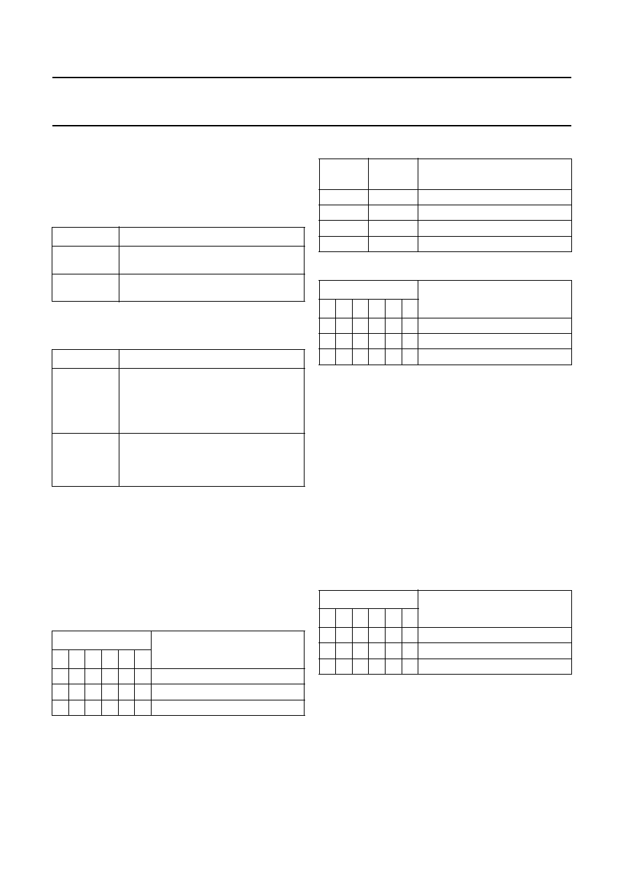
1999 Jun 11
50
Philips Semiconductors
Product specification
Microcontrollers for NTSC TVs with On-Screen
Display (OSD) and Closed Caption (CC)
P8xCx70 family
18.7.1
S
CREEN COLOUR DISPLAY AREA
The screen colour display area starts with a fixed offset of
8
µ
s from the leading edge of the horizontal sync pulse in
the horizontal direction. A vertical offset is not necessary.
Table 68 Screen colour display area
18.7.2
T
EXT DISPLAY AREA
Table 69 Text display area
The text area can be defined to start with an offset in both
the horizontal and vertical direction. The horizontal offset
is set in the Text Horizontal Position Register (see
Section 18.9.3). The offset is in full width characters
(1 to 64 characters) and quarter characters for fine setting
(0 to 3 quarters). The vertical offset is set in the Text
Vertical Position Register (see Section 18.9.2). The offset
is done in number of lines (0 to 63).
Table 70 Text area start offset
Note
1. The values `000000' to `000011' will result in a
corrupted offset.
POSITION
525-LINE
Horizontal
Start at 8
µ
s after leading edge of
HSYNC for 56
µ
s.
Vertical
Line 6, Field 1 (269, Field 2) to leading
edge of vertical sync.
POSITION
DESCRIPTION
Horizontal
Up to 48 full sized characters per row.
Start position setting from 3 to 64
characters from the leading edge of
HSYNC. Fine adjustment in quarter
characters.
Vertical
208 lines (nominal 38 to 245). Start
position setting from leading edge of
vertical sync, legal values are 4 to 64
lines.
TAS<5-0>
(1)
TEXT POSITION HORIZONTAL
TEXT AREA START
5
4
3
2
1
0
0
0
0
0
0
0
0 characters
1
1
1
1
1
1
63 characters
Table 71 Text area fine offset
Table 72 Text vertical position
The width of the text area is defined by setting the end
character value (1 to 64 characters). This number
determines where the background colour will end if set to
extend to the end of the row. It will also terminate the
character fetch process thus eliminating the necessity of a
row end attribute. This entails however writing to all
positions.
The text area end is set by the TAE0 to TAE5 bits in the
Text Area End Register (see Section 18.9.5). The width is
the difference between the horizontal offset and the end
value and is always as a number of full width characters
(0 to 48 valid range). The quarter character offset in the
Text Horizontal Position Register is also valid for the end
position.
Table 73 Text area end
HOP1
HOP0
TEXT POSITION HORIZONTAL
FINE OFFSET
0
0
0 quarters
0
1
1 quarter
1
0
2 quarters
1
1
3 quarters
VOL<5-0>
TEXT AREA VERTICAL LINE
OFFSET
5
4
3
2
1
0
0
0
0
0
0
0
0 lines
1
1
1
1
1
1
63 lines
TAE<5-0>
TEXT AREA END
FULL CHARACTERS
5
4
3
2
1
0
0
0
0
0
0
0
1 character
1
1
1
1
1
1
64 characters

1999 Jun 11
51
Philips Semiconductors
Product specification
Microcontrollers for NTSC TVs with On-Screen
Display (OSD) and Closed Caption (CC)
P8xCx70 family
18.8
General controls
18.8.1
P
OLARITY OF
HSYNC
AND
VSYNC
INPUT SIGNALS
The horizontal and vertical input sync signals can be
inverted by setting the HPOL and VPOL bits in the Text
Vertical Position Register (see Section 18.9.2).
Table 74 Sync signal polarity
18.8.2
F
RAME RESET GENERATION
Normally, VSYNC of the first field occurs during the first
half line period and Vsync of the second field occurs during
the second half period of a scan-line. In this case it is very
easy to generate a frame reset signal. The VSYNC pulse
is generated by sampling and rising edge detection.
HPOL
VPOL
SYNC SIGNAL POLARITY
0
0
input polarity
1
1
input inverted polarity
These VSYNC pulses are gated (AND gate) with a line
frequency signal which has a duty cycle of 50 : 50 (H50).
The output signal is the frame reset pulse. The rising edge
of the H50 signal is generated from the HSYNC pulse.
The falling edge is generated via a comparison between
the fixed value of half of the nominal number of 768 pixels
per line (comparator value: 384 pixels) and the value of a
pixel counter.
If the VSYNC of one field occurs shortly after the falling
edge of H50 and the line period has more than the nominal
number of 768 pixels per line, it is possible that both
VSYNC pulses occur during the low period of H50.
The result is that no frame reset pulse is generated. In the
case of a VSYNC pulse occurring shortly after the rising
edge of H50 and less than the nominal number of
768 pixels per line it is possible that every VSYNC pulse
will generate a frame reset pulse. To prevent this
happening the position of H50 is adjustable in increments
of 12 clock cycles. The adjustment value is selected using
the Odd/Even Align Register.
Fig.22 Frame reset timing.
handbook, full pagewidth
MGL151
Hsync
Frame
reset
Field 1
H50
Vsync_In
Vsync
(sampled)
Hsync
Frame
reset
Field 2
H50
Vsync_In
Vsync
(sampled)

1999 Jun 11
52
Philips Semiconductors
Product specification
Microcontrollers for NTSC TVs with On-Screen
Display (OSD) and Closed Caption (CC)
P8xCx70 family
18.9
Register descriptions
All registers are read/writeable. When the registers are read a value will be returned that will correspond to the written
data. There is one exception; when the Status Register is read, status information will be returned.
18.9.1
D
ISPLAY
C
ONTROL
R
EGISTER
(DCR)
Table 75 Display Control Register (address 87F0H)
Table 76 Description of DCR bits
18.9.2
T
EXT
V
ERTICAL
P
OSITION
R
EGISTER
(TVPR)
Table 77 Text Vertical Position Register (address 87F1H)
Table 78 Description of TVPR bits
7
6
5
4
3
2
1
B0
SRC3
SRC2
SRC1
SRC0
FLF
MSH
MOD1
MOD0
BIT
SYMBOL
DESCRIPTION
7
SCR3
Screen colour. These 4 bits select the screen colour; one of 16 colours may be
selected; see Table 59.
6
SCR2
5
SCR1
4
SCR0
3
FLF
Flash frequency. The state of this bit determines the flash frequency of the screen.
A frequency of 1 or 2 Hz can be selected; see Table 60.
2
MSH
Meshing. If MSH = 1, meshing is selected. See Section 18.2.12.
1
MOD1
Display modes. These 2 bits select one of the four display modes: Video mode, Full
Text mode, Mixed Screen mode and Mixed Video mode; see Table 56.
0
MOD0
7
6
5
4
3
1
0
VPOL
HPOL
VOL5
VOL4
VOL3
VOL2
VOL1
VOL0
BIT
SYMBOL
DESCRIPTION
7
VPOL
Vertical sync polarity. The state of this bit determines whether the vertical sync input is
inverted or not; see Table 74.
6
HPOL
Horizontal sync polarity. The state of this bit determines whether the horizontal sync
input is inverted or not; see Table 74.
5
VOL5
Vertical offset. These 6 bits select the number of lines that the text area is offset
vertically; see Table 72.
4
VOL4
3
VOL3
2
VOL2
1
VOL1
0
VOL0

1999 Jun 11
53
Philips Semiconductors
Product specification
Microcontrollers for NTSC TVs with On-Screen
Display (OSD) and Closed Caption (CC)
P8xCx70 family
18.9.3
T
EXT
H
ORIZONTAL
P
OSITION
R
EGISTER
(THPR)
Table 79 Text Horizontal Position Register (address 87F2H)
Table 80 Description of THPR bits
18.9.4
F
RINGING
C
ONTROL
R
EGISTER
(FCR)
Table 81 Fringing Control Register (address 87F3H)
Table 82 Description of FCR bits
7
6
5
4
3
2
1
0
HOP1
HOP0
TAS5
TAS4
TAS3
TAS2
TAS1
TAS0
BIT
SYMBOL
DESCRIPTION
7
HOP1
Fine horizontal offset. These 2 bits select a fine offset, ranging from 0 to 3 quarter
characters; see Table 71.
6
HOP0
5
TAS5
Text area start. These 6 bits select an offset of 0 to 63 full-width characters; see
Table 70.
4
TAS4
3
TAS3
2
TAS2
1
TAS1
0
TAS0
7
6
5
4
3
2
1
0
FRC3
FRC2
FRC1
FRC0
FRDN
FRDE
FRDS
FRDW
BIT
SYMBOL
DESCRIPTION
7
FRC3
Fringing colour. These 4 bits select the fringing colour. One of 16 colours can be
specified; see Table 58.
6
FRC2
5
FRC1
4
FRC0
3
FRDN
Fringing directions. The fringing direction is selected by setting one of these bits to a
logic 1. For example, when FRDN = 1, the fringing direction is North. See Table 57.
2
FRDE
1
FRDS
0
FRDW

1999 Jun 11
54
Philips Semiconductors
Product specification
Microcontrollers for NTSC TVs with On-Screen
Display (OSD) and Closed Caption (CC)
P8xCx70 family
18.9.5
T
EXT
A
REA
E
ND
R
EGISTER
(TAER)
Table 83 Text Area End Register (address 87F4H)
Table 84 Description of TAER bits
18.9.6
S
OFT
S
CROLL
A
REA
C
ONTROL
R
EGISTER
(SSACR)
Table 85 Soft Scroll Area Control Register (address 87F5H)
Table 86 Description of SSACR bits
7
6
5
4
3
2
1
0
-
-
TAE5
TAE4
TAE3
TAE2
TAE1
TAE0
BIT
SYMBOL
DESCRIPTION
7
-
These 2 bits are reserved.
6
-
5
TAE5
Text area end. These 6 bits assist in defining the width of the text area. The actual text
area width is the difference between the horizontal offset and the value specified by
these 6 bits; see Table 73.
4
TAE4
3
TAE3
2
TAE2
1
TAE1
0
TAE0
7
6
5
4
2
1
0
SSH3
SSH2
SSH1
SSH0
SSP3
SSP2
SSP1
SSP0
BIT
SYMBOL
DESCRIPTION
7
SSH3
Soft scroll area height. These 4 bits determine the visible scroll area height. One of
16 rows may be specified; see Table 64.
6
SSH2
5
SSH1
4
SSH0
3
SSP3
Soft scroll area position. These 4 bits specify the top display row of the soft scroll
area. One of 16 rows may be specified; see Table 63.
2
SSP2
1
SSP1
0
SSP0

1999 Jun 11
55
Philips Semiconductors
Product specification
Microcontrollers for NTSC TVs with On-Screen
Display (OSD) and Closed Caption (CC)
P8xCx70 family
18.9.7
S
CROLL
R
OWS
R
ANGE
R
EGISTER
(SRRR)
Table 87 Scroll Rows Range Register (address 87F6H)
Table 88 Description of SRRR bits
18.9.8
RGB B
RIGHTNESS
R
EGISTER
(BR)
Table 89 RGB Brightness Register (address 87F7H)
Table 90 Description of BR bits
7
6
5
4
3
2
1
0
SPS3
SPS2
SPS1
SPS0
STS3
STS2
STS1
STS0
BIT
SYMBOL
DESCRIPTION
7
SPS3
Stop scroll row. These 4 bits select the row number at which scrolling will stop. One of
16 rows can be specified; see Table 66.
6
SPS2
5
SPS1
4
SPS0
3
STS3
Start scroll row. These 4 bits select the row number at which scrolling will begin.
One of 16 rows can be specified; see Table 65.
2
STS2
1
STS1
0
STS0
7
6
5
4
3
2
1
0
FBPOL
-
-
-
BRI3
BRI2
BRI1
BRI0
BIT
SYMBOL
DESCRIPTION
7
FBPOL
Fast Blanking polarity. The state of this bit determines whether the polarity of the Fast
Blanking signal (FBL) is inverted or not; see Table 51.
6
-
These 3 bits are reserved.
5
-
4
-
3
BRI3
Brightness value. These 4 bits select the brightness value of the RGB output voltages.
One of 16 brightness values can be selected; see Table 52.
2
BRI2
1
BRI1
0
BRI0

1999 Jun 11
56
Philips Semiconductors
Product specification
Microcontrollers for NTSC TVs with On-Screen
Display (OSD) and Closed Caption (CC)
P8xCx70 family
18.9.9
S
TATUS
R
EGISTER
(SR)
A status register is provided that holds information that the processor can use to regulate the way data is written into the
display unit. The register is split into a read only and write only register. Both use the same address.
Table 91 Status Register (address 87F8H); read only
Table 92 Description of SR bits
7
6
5
4
3
2
1
0
BUSY
-
FIELD
SCRL
SCR3
SCR2
SCR1
SCR0
BIT
SYMBOL
DESCRIPTION
7
BUSY
Character display active or vertical sync. If BUSY = 0, this indicates that the
processor can access the display unit without causing effects on the screen. The lead
time is 4 ms, this is implemented to allow the microcontroller to finish the current access
to the display memory. Two modes are provided to switch between the text horizontal
blank area or vertical blank area.
6
-
Random information.
5
FIELD
1st or 2nd Field of vertical frame.
4
SCRL
Scroll busy. If SCRL = 1, this bit indicates that the scroll function is in progress. When
this bit is set, the automatic scroll function is started. It is automatically cleared on
completion. If forced to a logic 0, the scroll function will be terminated as if all lines were
scrolled. Subsequent logic 0 writes will cause the scroll row to increment by one.
3
SCR3
First scroll row select. The value specified by these 4 bits selects the actual row that is
the first one to be displayed in the scroll area. This value is modified by the automatic
scroll function.
2
SCR2
1
SCR1
0
SCR0

1999 Jun 11
57
Philips Semiconductors
Product specification
Microcontrollers for NTSC TVs with On-Screen
Display (OSD) and Closed Caption (CC)
P8xCx70 family
Table 93
Status Register (address 87F8H); write only
Table 94 Description of SR bits
18.9.10
HSYNC D
ELAY
R
EGISTER
(HSDR)
Table 95 HSYNC Delay Register (address 87FCH)
Table 96 Description of HSDR bits
7
6
5
4
3
2
1
0
-
H/V
SCON
SCRL
-
-
-
-
BIT
SYMBOL
DESCRIPTION
7
-
This bit is not used and causes no action.
6
H/V
Busy signal switch horizontal/vertical. If H/V = 0, horizontal blank area selected.
If H/V = 1, vertical blank area selected.
5
SCON
Scroll area enabled. If SCON = 1, then the scroll area is enabled.
See Section 18.5.1.2.
4
SCRL
Start scroll. If SCRL = 1, this bit indicates that the scroll function is in progress. When
this bit is set, the automatic scroll function is started. It is automatically cleared on
completion. If forced to a logic 0, the scroll function will be terminated as if all lines were
scrolled. Subsequent logic 0 writes will cause the scroll row to increment by one.
3
-
These 4 bits are not used and cause no action.
2
-
1
-
0
-
7
6
5
4
3
2
1
0
-
HSD6
HSD5
HSD4
HSD3
HSD2
HSD1
HSD0
BIT
SYMBOL
DESCRIPTION
7
-
reserved
6
HSD6
HSYNC delay. These 7 bits allow the position of the HSYNC pulse to be changed in
increments of full width characters. A delay of 0 to 63 full width characters can be
selected.
5
HSD5
4
HSD4
3
HSD3
2
HSD2
1
HSD1
0
HSD0

1999 Jun 11
58
Philips Semiconductors
Product specification
Microcontrollers for NTSC TVs with On-Screen
Display (OSD) and Closed Caption (CC)
P8xCx70 family
18.9.11
O
DD
/E
VEN
A
LIGN
R
EGISTER
(OEAR)
Table 97 Odd/Even Align Register (87FDH)
Table 98 Description of OEAR bits
7
6
5
4
3
2
1
0
-
OEA6
OEA5
OEA4
OEA3
OEA2
OEA1
OEA0
BIT
SYMBOL
DESCRIPTION
7
-
reserved
6
OEA6
H50 delay. These 7 bits allow the position of the H50 pulse to be changed in increments
of 12 clock pulses.
5
OEA5
4
OEA4
3
OEA3
2
OEA2
1
OEA1
0
OEA0

1999 Jun 11
59
Philips Semiconductors
Product specification
Microcontrollers for NTSC TVs with On-Screen
Display (OSD) and Closed Caption (CC)
P8xCx70 family
18.9.12
C
ONFIGURATION
R
EGISTER
(CONFR)
The Configuration Register is provided for special purposes and to program the delay between the RGB and FBL output.
Table 99 Configuration Register (address 87FFH)
Table 100 Description of CONFR bits
Table 101 FBL delay adjustment
7
6
5
4
3
2
1
0
CC
PLUS
ADJ
MIN
-
-
-
-
BIT
SYMBOL
DESCRIPTION
7
CC
Closed Caption mode. The state of this bit selects the OSD mode or the CC mode.
If CC = 0, then the OSD mode is selected; this is also the default setting. If CC = 1, then
the CC mode is selected. In the CC mode the underline is suppressed during the
display of a serial attribute. The display is then according to the CC specification.
6
PLUS
FBL delay select. These 3 bits define the timing of the FBL signal; see Table 101.
5
ADJ
4
MIN
3
-
Reserved, set to logic 0.
2
-
These 3 bits are used for test purposes only and should be set to logic 0s for normal
operation.
1
-
0
-
PLUS
ADJ
MIN
FBL TIMING
0
0
0
FBL switched to video, not active.
0
0
1
FBL active one pixel early to RGB.
0
1
0
FBL synchronous with RGB (typical setting).
1
0
0
FBL active one pixel delayed to RGB.
X
X
X
All other combinations are allowed and will have the effect that the above
settings are functionally ORed, e.g. `111' will result in a 3 pixel wide FBL
pulse when one single pixel is displayed.

1999 Jun 11
60
Philips Semiconductors
Product specification
Microcontrollers for NTSC TVs with On-Screen
Display (OSD) and Closed Caption (CC)
P8xCx70 family
18.10 Character font format
The character font is a 12 (horizontal) x 13 (vertical)
matrix. The ROM contents have two extra lines in each
field to facilitate the fringing function when groups of
characters are used to build symbols.
A table with 128 characters, two columns of special
characters (32) and a column for proportional spaced
characters (16) is shown in Fig.27.
The ROM size is 176 characters x 12
◊
16 = 33792 bits
(4224 bytes, 2816 x 12-bit words).
18.10.1 C
HARACTER
ROM
FORMAT
The character addressing scheme is dependent on what
type of character is accessed. Therefore, the ROM format
for the different columns changes respectively.
The ROM format is 16 locations in words of 12 bits, where
the MSB (bit 11) of the ROM word is the left most pixel of
a character displayed.
The lines 0 and 14 are used for fringing of clustered
characters (single images using more than one character)
over row boundaries. Lines 1 to 13 contain the font of the
character and line 15 is not used.
The proportional spaced characters use only bits 11 to 6
for display. Bits 5 to 0 are defined by repeating the
information held in bits 11 to 6 shifted up one line.
The ROM definition for these characters is shown in
Fig.24. Proportional characters can be displayed in
column A only.
The ROM format for the special characters uses two
subsequent character ROM locations. The character
definition will always start with an even character.
This location holds the information for bit Plane 0 the next
location (odd) contains the bit Plane 1. No shadowing is
supported when using these characters. The bit
combinations of Plane 0 and Plane 1 define which colour
is displayed for a certain pixel. A detailed description on
how these characters are displayed is found in
Section 18.2.16.
The ROM format for each plane is defined as stated for the
normal characters, except that the data on the fringing
lines is ignored.
Fig.23 Character ROM format columns 0 to 7.
handbook, halfpage
line 13 from
character above
line 0 from
character below
top left
pixel
MSB
LSB
MGL153
HEX
440
003
00C
030
0C0
300
C00
C00
300
0C0
030
00C
003
000
198
000
line
number
0
1
2
3
4
5
6
7
8
9
10
11
12
13
14
15
fringing
top line
bottom right
pixel
bottom line
fringing
line not used
Fig.24 Proportional character ROM format
column A.
handbook, halfpage
0 (LSB)
5
6
11 (MSB)
MGL154
HEX
value
000
fringe
(1)
fringe
(3)
fringe
(2)
not used
not used
000
00C
300
00C
30C
30C
30C
30C
30C
306
180
000
000
000
000
line
number
0
1
2
3
4
5
6
7
8
9
10
11
12
13
14
15
(1) Line 13 from character above.
(2) Line repeated from line 14 (bits 11 to 6).
(3) Line 1 from character below.

1999 Jun 11
61
Philips Semiconductors
Product specification
Microcontrollers for NTSC TVs with On-Screen
Display (OSD) and Closed Caption (CC)
P8xCx70 family
18.10.2 ROM
ADDRESSING
Figures 25 and 26 illustrate the addressing schemes used to access the different character formats. Figure 25 shows the
ROM organization of the normal and proportional spaced characters and Fig.26 shows the ROM organization of the
special characters. The address calculation in on the basis of word access. If the CPU accesses the ROM, a two byte
access must be performed to capture the data, the data format is according to the definition in Fig.19.
Fig.25 Character ROM organisation.
handbook, halfpage
character X
word address = C000H
word address = (X
◊
16)
+
C000H
word address = [(X
+
1)
◊
16]
+
C000H
X = 0, 1, 2, 3,....
12 bits
MGL155
character X
+
1
Fig.26 Character ROM organization for
columns 8 and 9.
handbook, halfpage
character X
plane 0
word address = C000H
word address = (X
◊
16) + C000H
word address = [(X + 1)
◊
16] + C000H
X = 0, 2, 4,....
12 bits
MGL156
character X
plane 1
Fig.27 Character table.
handbook, full pagewidth
MGR275
0
0
1
2
3
4
5
6
7
8 (B)
9 (C)
A (D)
Æ
SP
0
@
P
˙
p
∞
!
1
A
Q
a
q
1/2
"
2
B
R
b
r
ø
#
3
C
S
c
s
TM
$
4
D
T
d
t
¢
%
5
E
U
e
u
1
2
3
4
5
6
7
8
9
A
B
C
D
E
F
£
&
6
F
V
f
v
¥
7
G
W
g
w
ý
(
8
H
X
h
x
_
)
9
I
Y
i
y
Ë
·
:
J
Z
j
z
‚
+
;
K
[
k
Á
Í
,
<
L
È
l
Ó
-
=
M
]
m
—
Ù
.
>
N
Õ
n
Ò
˚
/
?
O
Û
o
n
Character code columns (bits 4 to 7)
Char
acter code ro
ws (bits 0 to 3)

1999 Jun 11
62
Philips Semiconductors
Product specification
Microcontrollers for NTSC TVs with On-Screen
Display (OSD) and Closed Caption (CC)
P8xCx70 family
19 MEMORY DATA BIT ALLOCATION
Table 102 Register map bit allocation
Table 103 Memory data/bit allocation
19.1
Interfaces
19.1.1
RGB
AND
B
LANKING
O
UTPUT
The RGB outputs are analog signals derived from a DAC. The output impedance depends on the switched value, but is
low enough to drive the colour decoder.
The polarity and the delay between RGB outputs and the blanking output is programmable. The default setting is active
HIGH (RGB on).
ADDR.
REGISTER NAME
7
6
5
4
3
2
1
0
87F0H
Display Control
SRC3
SRC2
SRC1
SRC0
FLF
MSH
MOD1
MOD0
87F1H
Text Vertical Position
VPOL
HPOL
VOL5
VOL4
VOL3
VOL2
VOL1
VOL0
87F2H
Text Horizontal Position
HOP1
HOP0
TAS5
TAS4
TAS3
TAS2
TAS1
TAS0
87F3H
Fringing Control
FRC3
FRC2
FRC1
FRC0
FRDN
FRDE
FRDS
FRDW
87F4H
Text Area End
-
-
TAE5
TAE4
TAE3
TAE2
TAE1
TAE0
87F5H
Scroll Area
SSH3
SSH2
SSH1
SSH0
SSP3
SSP2
SSP1
SSP0
87F6H
Scroll Range
SPS3
SPS2
SPS1
SPS0
STS3
STS2
STS1
STS0
87F7H
RGB Brightness
FBPOL
-
-
-
BRI3
BRI2
BRI1
BRI0
87F8H
Status (read)
BUSY
-
FIELD
SCRL
SCR3
SCR2
SCR1
SCR0
87F8H
Status (write)
-
H/V
SCON
SCRL
-
-
-
-
87FCH
HSYNC Delay
-
HSD6
HSD5
HSD4
HSD3
HSD2
HSD1
HSD0
87FDH
Odd/Even Align
-
OEA6
OEA5
OEA4
OEA3
OEA2
OEA1
OEA0
87FEH
Reserved
-
-
-
-
-
-
-
-
87FFH
Configuration Register
CC
PLUS
ADJ
MIN
-
-
-
-
ODD BYTE BITS 3 TO 0
EVEN BYTE BITS 7 TO 0
B11
B10
B9
B8
B7
B6
B5
B4
B3
B2
B1
B0
Valid for byte address 8000H to 801FH in display memory: Scroll map
En.
-
ptr9
ptr8
ptr7
ptr6
ptr5
ptr4
ptr3
ptr2
ptr1
ptr0
Valid for byte address 8020H to 8460H in display memory: Display page, first column position
1 = ser.
1 = at
eof
bgc
for3
box
vert. sync hor.sync
back3
back2
back1
back0
Valid for byte address 8020H to 8460H in display memory: Display page, all columns
0 = par. for3
for2
for1
chr7
chr6
chr5
chr4
chr3
chr2
chr1
chr0
1 = ser.
0 = at
fringing
italic
flash
box
overline
underline back3
back2
back1
back0
Valid for byte address 8020H to 8460H in display memory: Display page, all columns except first position
1 = ser.
1 = after eof
bgc
for3
box
overline
underline back3
back2
back1
back0
Valid for byte address 8700H to 871FH: CLUT
red3
red2
red1
red0
green3
green2
green1
green0
blue3
blue2
blue1
blue0

1999 Jun 11
63
Philips Semiconductors
Product specification
Microcontrollers for NTSC TVs with On-Screen
Display (OSD) and Closed Caption (CC)
P8xCx70 family
20 PROGRAMMER
The P87Cx70 OTP contains two EPROM modules, one
64-kbyte system EPROM and one 8-kbyte character
EPROM.
Users can program or verify both system and character
EPROM with a PC using Intel HEX format.
20.1
EPROM Interface
Port 0 and Port 2 are used as the 16-bit address bus;
Port 0 for the higher address byte and Port 2 for the lower
address byte. Port 3 is used as an 8-bit bidirectional data
bus during programming and verify operations.
For control signals, ALE/PROG is used as the write strobe
(WE) and P1.0 is used as the output enable (OE). Pin 28
is the programming voltage (V
PP
) input and requires
12.75 V during the Programming mode and 5 V during the
Verification mode. The required input on the RESET,
PSEN and P1.0 to P1.4 pins is dependent upon the mode
selected.
Signal states for the three modes are specified in
Table 104 and the timing characteristics of these signals
are detailed in Section 20.5.
20.2
OTP application mode
The OTP application mode consists of two major
sub-modes: Programming mode and Verify mode.
The pin assignment during OTP programming and
verification operations is specified in Table 105.
20.2.1
P
ROGRAMMING MODE
The Programming mode performs three operations: main
64-kbyte OTP, extra row programming and select two
bytes programming.
The main 64-kbyte OTP operation is the core function of
programming. The customer can program the software
using an EPROM writer. Extra row programming is similar
to test ROM in mask ROM and can be used to store
production IDs, testing patterns etc. The select two bytes
programming operation is used to speed up the
programming of the checker board.
The Programming configuration is shown in Fig.28.
20.2.2
V
ERIFY MODE
The Verify mode performs two operations: Program verify
and Extra row read. The program verify operation checks
that the value programmed is correct. The Extra row read
mode is similar to the Program verify mode and ensures
that the extra row programming is correct.
The Program verification configuration is shown in Fig.29.
20.3
Programming format for character EPROM
The character EPROM programming data format contains
12-bit OSD data for each character row; 4 bits from OSDH
and 8 bits from OSDL. The encoding sequence is shown
in Fig.30.
The address range of the 8-kbyte character EPROM is
from C000H to DFFFH.
20.4
Programming format for system EPROM
The system EPROM format is the same as for normal
EPROM and is programmed sequentially using Intel Hex
format.
The address range of the 64-kbyte system EPROM is from
0000H to FFFFH.
Table 104 OTP function table
OPERATION MODE
RESET
PSEN
ALE/WE
EA/V
PP
P1.3
P1.2
P1.1
P1.0/OE
Programming
1
0
LOW pulse
V
PP
1
1
1
H
Program verify
1
0
H
V
DD
1
1
1
LOW pulse
2-byte programming
1
0
LOW pulse
V
PP
0
0
1
H

1999 Jun 11
64
Philips Semiconductors
Product specification
Microcontrollers for NTSC TVs with On-Screen
Display (OSD) and Closed Caption (CC)
P8xCx70 family
Table 105 Pin assignment during programming and verification operations
SYMBOL
PIN
SYSTEM EPROM
OSD EPROM
P0.0
1
A8
A8
P0.1
2
A9
A9
P0.2
3
A10
A10
P0.3
4
A11
A11
P0.4
5
A12
A12
P0.5
6
A13
(LOW)
P0.6
7
A14
(HIGH)
P0.7
8
A15
(HIGH)
P1.0
9
OE
OE
P1.1
10
OTP SEL0
OTP SEL0
P1.2
11
OTP SEL1
OTP SEL1
P1.3
12
OTP SEL2
OTP SEL2
P1.4
30
(LOW)
(HIGH)
P2.0
21
A0
A0
P2.1
20
A1
A1
P2.2
19
A2
A2
P2.3
18
A3
A3
P2.4
17
A4
A4
P2.5
16
A5
A5
P2.6
15
A6
A6
P2.7
14
A7
A7
P3.0
45
D0
D0
P3.1
46
D1
D1
P3.2
47
D2
D2
P3.3
48
D3
D3
P3.4
49
D4
D4
P3.5
50
D5
D5
P3.6
51
D6
D6
P3.7
52
D7
D7
ALE/PROG
29
WE
WE
V
PP
/EA
28
V
PP
V
PP
RST
43
(HIGH)
(HIGH)
PSEN
27
(LOW)
(LOW)

1999 Jun 11
65
Philips Semiconductors
Product specification
Microcontrollers for NTSC TVs with On-Screen
Display (OSD) and Closed Caption (CC)
P8xCx70 family
Fig.28 Programming configuration.
handbook, full pagewidth
MGR376
P87C770
(OTP)
P2.7 to P2.0
P0.7 to P0.0
1
A7 to A0
L-pulse
1
1
1
1
1/0
P3.7 to P3.0
P1.4
P1.2
P1.1
P1.0
P1.3
D7 to D0
0
12.75 V
A15 to A8
5 V
RESET
VSS
VDD
VPP/EA
PSEN
ALE/PROG
Fig.29 Program verification configuration.
handbook, full pagewidth
MGR377
P87C770
(OTP)
P2.7 to P2.0
P0.7 to P0.0
1
A7 to A0
1
1
1
0
1
1
1/0
P3.7 to P3.0
P1.4
P1.2
P1.1
P1.0
P1.3
D7 to D0
0
5 V
A15 to A8
5 V
RESET
VSS
VDD
VPP/EA
PSEN
ALE/PROG

1999 Jun 11
66
Philips Semiconductors
Product specification
Microcontrollers for NTSC TVs with On-Screen
Display (OSD) and Closed Caption (CC)
P8xCx70 family
Fig.30 Data format of character EPROM.
handbook, full pagewidth
MGR375
OSDL
(HEX)
OSDL
<7 to 0>
OSDH
<3 to 0>
11
0
3
7
13
15
8 7
1 0
OSDH
(HEX)
00 - 00
03 - 00
83 - 01
C3 - 00
60 - 00
07 - 00
08 - 00
E8 - 07
08 - 00
07 - 00
60 - 00
C3 - 00
83 - 01
03 - 00
00 - 00
00 - 00
00 00 03 00 83 01 C3 00 60 00 07 00 08 00 E8 07
08 00 07 00 60 00 C3 00 83 01 03 00 00 00 00 00
:10 C000 00
:10 C010 00
:10 CFFF 00

1999 Jun 11
67
Philips Semiconductors
Product specification
Microcontrollers for NTSC TVs with On-Screen
Display (OSD) and Closed Caption (CC)
P8xCx70 family
20.5
EPROM timing characteristics
Table 106 EPROM programming timing
SYMBOL
PARAMETER
MIN.
TYP.
MAX.
UNIT
t
su(A)
address set-up time
2
-
-
µ
s
t
h(A)
address hold time
20
-
-
ns
t
su(OE)
output enable set-up time
2
-
-
µ
s
t
su(CE)
chip enable set-up time
2
-
-
µ
s
t
W(P)
program pulse width (typically 5 programming pulses)
95
100
105
µ
s
t
su(PV)
program voltage set-up time
2
-
-
µ
s
t
h(WE)
write enable hold time
110
-
-
ns
t
su(D)
data set-up time
2
-
-
µ
s
t
h(D)
data hold time
20
-
-
ns
t
W(OE)
output enable pulse width
300
-
-
ns
t
ACC(OE)
output enable access verify
92
122
183
ns
t
OZ
output to high-impedance verify
10
-
-
ns
Fig.31 EPROM programming timing diagram.
handbook, full pagewidth
MGR374
tOZ
tACC(OE)
th(D)
th(A)
th(WE)
tsu(D)
tsu(CE)
5 V
PROGRAMMING
VERIFY
WE
(ALE/PROG)
VPP/EA
12.75 V
address
(Ports 0 and 2)
CE
(internal signal)
OE
(P10)
data I/O
(Port 3)
tW(P)
tsu(A)
tsu(PV)
data in for EPROM
address
data out from EPROM
tsu(OE)
tW(OE)

1999 Jun 11
68
Philips Semiconductors
Product specification
Microcontrollers for NTSC TVs with On-Screen
Display (OSD) and Closed Caption (CC)
P8xCx70 family
Fig.32 Programming pinning configuration.
handbook, halfpage
P8xC770
MGR373
1
2
3
4
5
6
7
8
9
10
11
12
13
14
15
16
17
18
19
20
21
22
23
24
25
26
52
51
50
49
48
47
46
45
44
43
42
41
40
39
38
37
36
35
34
33
32
31
30
29
28
27
A8
A9
A10
A11
A12
A13
A14
A15
P1.0/AFT0
P1.1/AFT1
P1.2/AFT2
P1.3/PWM0
VSSD
A7
A6
A5
A4
A3
A2
A1
A0
VSSA
CVBS
STN
BLK
IREF
D7
D6
D5
D4
D3
D2
D1
D0
VDDC
RESET
XI
XO
VSSD
VDDP
VDDA
VSYNC
HSYNC
FB
R
G
B
REFH
P1.4
ALE/PROG
VPP/EA
PSEN

1999 Jun 11
69
Philips Semiconductors
Product specification
Microcontrollers for NTSC TVs with On-Screen
Display (OSD) and Closed Caption (CC)
P8xCx70 family
Table 107 Programming configuration pin descriptions
SYMBOL
PIN
I/O
DESCRIPTION
P0.0 to P0.7
1 to 8
I/O
address lines A8 to A15
P1.0/AFT0
9
I/O
Port line P1.0; alternative function as 4-bit AFT0 input
P1.1/AFT1
10
I/O
Port line P1.1; alternative function as 4-bit AFT1 input
P1.2/AFT2
11
I/O
Port line P1.2; alternative function as 4-bit AFT2 input
P1.3/PWM0
12
I/O
Port line P1.3 (open-drain, bidirectional); alternative function as 7-bit PWM
output
V
SSD
13
-
digital ground
P2.7 to P2.0
14 to 21
I/O
address lines A7 to A0
V
SSA
22
-
analog ground
CVBS
23
I
composite video input
STN
24
I
Data Slicer decoupling capacitor input, connect to V
SSA
via a 100 nF capacitor.
BLK
25
I
CVBS signal black level reference, connect to V
SSA
via a 100 nF capacitor.
IREF
26
I
CVBS signal reference current input, connect to V
SSA
via a 27 k
resistor.
PSEN
27
O
Program Store Enable (active LOW) is bonded out for testing purpose only.
V
PP
/EA
28
I
External Access (active LOW) is bonded out for testing purpose only; this pin is
also used for the 12.75 V programming voltage supply in program/font OTP
programming modes.
ALE/PROG
29
I/O
Address Latch Enable is bonded out for testing purposes only; this pin is also
used for programming pulses input in program/font OTP programming modes.
P1.4
30
I/O
Port line P1.4 (open-drain, bidirectional)
REFH
31
I
Data Slicer reference high capacitor input, connect to V
SSA
via a 100 nF
capacitor.
B
32
O
CC/OSD Blue colour current output
G
33
O
CC/OSD Green colour current output
R
34
O
CC/OSD Red colour current output
FB
35
O
CC/OSD fast blanking output
HSYNC
36
I
TV horizontal sync input (for OSD synchronization)
VSYNC
37
I
TV vertical sync input (for OSD synchronization)
V
DDA
38
-
5 V analog power supply
V
DDP
39
-
5 V digital power supply
V
SSD
40
I
digital ground
XO
41
O
system oscillator crystal output
XI
42
I
system oscillator crystal input
RESET
43
I
reset input (active HIGH)
V
DDC
44
-
5 V digital power supply
P3.0 to P3.7
45 to 52
I/O
data I/O lines, D0 to D7

1999 Jun 11
70
Philips Semiconductors
Product specification
Microcontrollers for NTSC TVs with On-Screen
Display (OSD) and Closed Caption (CC)
P8xCx70 family
21 LIMITING VALUES
22 DC CHARACTERISTICS
V
DD
= 4.5 to 5.5 V; V
SS
= 0 V; T
amb
=
-
20 to +70
∞
C. All voltages with respect to V
SS
, unless otherwise specified.
SYMBOL
PARAMETER
CONDITIONS
MIN.
MAX.
UNIT
V
DD
supply voltage
-
0.5
+7.0
V
V
i
input voltage on any pin with respect to
ground (V
SS
)
-
0.5
V
DD
+ 0.5
V
P
tot
total power dissipation
-
700
mW
T
stg
storage temperature
-
55
+125
∞
C
T
amb
operation ambient temperature
-
20
+70
∞
C
V
esd
electrostatic protection HBM
leakage < 1
µ
A
-
2000
+2000
V
electrostatic protection MM
leakage < 1
µ
A
-
250
+250
V
SYMBOL
PARAMETER
CONDITIONS
MIN.
TYP.
MAX.
UNIT
Supply
V
DDC
digital core supply voltage
4.5
5.0
5.5
V
I
DDC
digital supply current
-
47
-
mA
V
DDP
peripheral supply voltage
4.5
5.0
5.5
V
I
DDP
peripheral supply current
-
20
-
mA
V
DDA
analog supply voltage
4.5
5.0
5.5
V
I
DDA
analog supply current
-
9
-
mA
Ports 1, 2 and 3 inputs
V
IL
LOW-level input voltage
0
-
0.3V
DD
V
V
IH
HIGH-level input voltage
0.7V
DD
-
V
DD
V
I
LI
input leakage current
V
SS
< V
I
< V
DD
-
10
-
+10
µ
A
Ports 1, 2 and 3 outputs (open-drain)
V
OL
LOW-level output voltage
I
OL
= 3 mA
-
-
0.4
V
Port 2 outputs
V
OL
LOW-level output voltage
I
OL
= 3 mA
-
-
0.4
V
I
OL
= 10 mA
-
-
1
V
ALE, PSEN and EA inputs
V
IL
LOW-level input voltage
0
-
0.3V
DD
V
V
IH
HIGH-level input voltage
0.7V
DD
-
V
DD
V
ALE, PSEN and EA outputs (open-drain)
V
OL
LOW-level output voltage
I
OL
= 3 mA
-
-
0.4
V
I
OL
= 10 mA
-
-
1
V

1999 Jun 11
71
Philips Semiconductors
Product specification
Microcontrollers for NTSC TVs with On-Screen
Display (OSD) and Closed Caption (CC)
P8xCx70 family
AFT inputs: P1.0/AFT0, P1.1/AFT1 and P1.2/AFT2
V
ai
comparator analog input
voltage
V
SS
-
V
DD
V
V
ae
conversion error range
P83C770
-
0.5
-
+0.5
LSB
P87C770
-
0.7
-
+0.7
LSB
R, G and B outputs (4-bit DAC current source)
I
OH
HIGH-level output source
current
-
8.9
-
mA
INL
integral non-linearity
-
1
/
2
0
+
1
/
2
LSB
DNL
differential non-linearity
-
1
/
2
0
+
1
/
2
LSB
matching RGB
-
1
/
2
-
+
1
/
2
LSB
FB output
I
OL
LOW-level output source
current
P83C770; V
O
= 0.4 V
-
7
-
mA
P87C770; V
O
= 0.4 V
-
14
-
mA
I
OH
HIGH-level output source
current
V
O
= V
DD
-
0.4 V
-
5
-
mA
RESET
V
IL
LOW-level input voltage
0
-
0.3V
DD
V
V
IH
HIGH-level input voltage
0.7V
DD
-
V
DD
V
R
rst
internal reset pull-down
resistor
50
-
200
k
HSYNC and VSYNC inputs
V
IL
LOW-level input voltage
-
0.3
-
0.8
V
V
IH
HIGH-level input voltage
3.15
-
V
DD
+ 0.5
V
I
LI
input leakage current
V
I
= 0 to V
DD
-
-
10
µ
A
C
in
input capacitance
-
-
5
pF
CVBS input
V
sync
sync amplitude
0.1
0.3
0.6
V
V
l(vid)
video input amplitude
(peak-to-peak value)
0.7
1.0
1.4
V
V
ldat
caption data amplitude
0.25
0.35
0.49
V
Z
source
source impedance
250
V
in
input switching level of
sync separator
1.8
2.15
2.5
V
Z
i
input impedance
2.5
5
-
k
C
i
input capacitance
-
-
10
pF
IREF input
R
IREF
external resistor to ground
-
27
-
k
V
IREF
voltage on pin
-
0.5V
DD
-
V
Power-on reset
V
t
trigger level
3.6
3.9
4.2
V
SYMBOL
PARAMETER
CONDITIONS
MIN.
TYP.
MAX.
UNIT

1999 Jun 11
72
Philips Semiconductors
Product specification
Microcontrollers for NTSC TVs with On-Screen
Display (OSD) and Closed Caption (CC)
P8xCx70 family
Fig.33 AFT conversion error range.
handbook, full pagewidth
MGR276
1
3/16
5/16
1/16
0
2
3
4
5
VDD
(volts)
7/16
9/16
11/16
13/16
15/16
14/16
16/16
actual
ideal
conversion error
range
<
0.5 LSB
conversion error
range
<
0.7 LSB
fraction of VDD
Fig.34 ADC error.
handbook, full pagewidth
MGR277
0.1
3/16
5/16
1/16
0
0.3
0.7
0.5
ADC error
(LSB)
7/16
9/16
11/16
13/16
15/16
14/16
16/16
fraction of VDD

1999 Jun 11
73
Philips Semiconductors
Product specification
Microcontrollers for NTSC TVs with On-Screen
Display (OSD) and Closed Caption (CC)
P8xCx70 family
23 AC CHARACTERISTICS
V
DD
= 4.5 to 5.5 V; V
SS
= 0 V; T
amb
=
-
20 to +70
∞
C. All voltages with respect to V
SS
, unless otherwise specified.
Note
1. Susceptibility for environment noise @ 1 V
PP
CVBS, 25
∞
C;12 MHz.
SYMBOL
PARAMETER
CONDITIONS
MIN.
TYP.
MAX.
UNIT
Ports 0, 1 and 3 outputs (open-drain)
t
f(o)
output fall time
C
L
= 35 pF; (slope control
implemented)
30
-
-
ns
ALE, PSEN and EA outputs (slope control implemented)
t
r(o)
output rise time
C
L
= 40 pF
-
-
-
ns
t
f(o)
output fall time
C
L
= 40 pF
30
-
-
ns
XI and XO
f
xtal
crystal frequency
-
12
-
MHz
AFT inputs: P1.0/AFT0, P1.1/AFT1 and P1.2/AFT2
T
AFT(con)
conversion time
f
xtal
= 12 MHz
-
8
-
µ
s
FB output
t
r(FB)
FB rise time
C
L
= 35 pF
-
4
-
ns
t
f(FB)
FB fall time
-
4
-
ns
CVBS Closed Caption behaviour
white noise (rms value)
-
-
60
mV
co-channel interface
(peak-to-peak value)
-
-
100
mV
PP
eye height
-
-
55
%
Power-on reset
T
r
POR response time
at power-on V
DD
: 0
5 V
5
-
-
µ
s
voltage spike V
DD
: 5 V
V
t
5
-
-
µ
s
t
W
POR pulse width
at power-on V
DD
: 0
5 V
10
-
-
µ
s
voltage spike V
DD
: 5 V
V
t
10
-
-
µ
s

1999 Jun 11
74
Philips Semiconductors
Product specification
Microcontrollers for NTSC TVs with On-Screen
Display (OSD) and Closed Caption (CC)
P8xCx70 family
24 APPLICATION INFORMATION
Fig.35 Application diagram.
handbook, full pagewidth
10 k
27 k
10 k
10 k
100 nF
100 nF
100 nF
22 pF
12
MHz
22 pF
47
µ
F
2.2
µ
H
P8XC770
MGR919
1
2
3
4
5
6
7
8
9
10
11
12
13
14
15
16
17
18
19
20
21
22
23
CVBS signal
24
25
26
5 V
5 V
5 V
52
51
50
49
48
47
46
45
44
43
42
41
40
39
38
37
36
35
34
33
32
31
30
29
28
27
P0.0/PWM8
P0.1/PWM7
P0.2/PWM6
P0.3/PWM5
P0.4/PWM4
P0.5/PWM3
P0.6/PWM2
P0.7/PWM1
P1.0/AFT0
P1.1/AFT1
P1.2/AFT2
P1.3/PWM0
VSSD
P2.7
P2.6
P2.5
P2.4
P2.3
P2.2
P2.1
P2.0
VSSA
CVBS
STN
BLK
IREF
P3.7
P3.6
P3.5/SDA
P3.4/SCL
P3.3/T1
P3.2/INT0
P3.1/T0
P3.0/INT1
VDDC
RESET
XI
XO
VSSD
VDDP
VDDA
VSYNC
HSYNC
FB
R
G
B
REFH
GNDA
100 nF
GNDA
GNDD
GNDD
GNDA
GNDA
GNDA
GNDD
P1.4
ALE/PROG
VPP/EA
PSEN
100 nF
GNDA

1999 Jun 11
75
Philips Semiconductors
Product specification
Microcontrollers for NTSC TVs with On-Screen
Display (OSD) and Closed Caption (CC)
P8xCx70 family
25 RELEASE LETTER OF ERRATA
25.1
Bugs with a software workaround
∑
The soft scroll active bit and the top scroll row are not
synchronized. Therefore, it is not possible to calculate
from this bit and the top scroll row the current base row
(the row which is displayed as the lowest one or which
scrolls in). The top scroll row number is incremented
immediately after the soft scroll function is finished but
the soft scroll active bit remains set. The soft scroll
active bit is cleared one field/frame later. A software
workaround is implemented.
∑
If the soft scroll function is to be stopped (write 0
◊
20 to
OSD Status Register) the soft scroll should stop
immediately, but it stops at the end of the field/frame.
After stopping the soft scroll function the soft scroll
active bit should be cleared and the top scroll row
number (lower 4 bit of the OSD Status Register) should
be incremented by one. But sometimes the top scroll
row number is incremented by two. Also in the stopped
soft scroll the display sometimes jumps out of the
defined scroll range. For example, the range is defined
from row 0 to 5 and row 8 to 14 is displayed.
A correction is possible after the next frame, which results
in the stopped soft scroll (0.2 after soft scroll has been
started a stop soft scroll is sent) to sometimes generate a
display flicker.
∑
Read/Write problem with access to Display Memory by
the CPU. The error rate is 1/84000 (synchronized
clock). The error is synchronous to the HSYNC with
approximately 11
µ
s delay after HSYNC.
The automatically incremented DPTR didn't work
correctly.
A move command to the display memory
(MOVX @DPTR,A) or (MOVX A, @DPTR) sometimes
delivers a wrong result (e.g. an `A' should be written/read
but a `B' is stored/read in/from the memory).
A software workaround has been designed.
25.2
Bugs with no workaround
∑
The foreground colour of the first character behind a
double size/width attribute is ignored.
∑
During a double height row, if shadow is active, a north
shadow appears above the last line of the row whether
the underline is active or not.
25.3
Specification problems (unspecified)
∑
Soft scroll function cannot be stopped immediately
(behaviour is not specified in the specification). If the
decoder wants to terminate the soft scroll function, the
soft scroll function stops one field/frame later. A restart
is not possible before the scrolling has stopped.
Therefore, a restart of the soft scroll function must be
delayed by one field/frame. A software workaround is
implemented.
According to the CC specification the time between stop
and start should be no more than 0.433 seconds.
With the method as implemented the start command will
be issued after 0.46 seconds.
∑
The OSD does not allow the active edges of HSYNC
and VSYNC to come at exactly the same moment
∑
Soft scroll does not work, if a double height row is the top
row of the scroll area.
The specification has been changed to `the soft scroll
function with double height rows is forbidden'.

1999 Jun 11
76
Philips Semiconductors
Product specification
Microcontrollers for NTSC TVs with On-Screen
Display (OSD) and Closed Caption (CC)
P8xCx70 family
26 PACKAGE OUTLINE
UNIT
b
1
c
E
e
M
H
L
REFERENCES
OUTLINE
VERSION
EUROPEAN
PROJECTION
ISSUE DATE
IEC
JEDEC
EIAJ
mm
DIMENSIONS (mm are the original dimensions)
SOT247-1
90-01-22
95-03-11
b
max.
w
M
E
e
1
1.3
0.8
0.53
0.40
0.32
0.23
47.9
47.1
14.0
13.7
3.2
2.8
0.18
1.778
15.24
15.80
15.24
17.15
15.90
1.73
5.08
0.51
4.0
M
H
c
(e )
1
M
E
A
L
seating plane
A
1
w
M
b
1
D
A
2
Z
52
1
27
26
b
E
pin 1 index
0
5
10 mm
scale
Note
1. Plastic or metal protrusions of 0.25 mm maximum per side are not included.
(1)
(1)
D
(1)
Z
e
A
max.
1
2
A
min.
A
max.
SDIP52: plastic shrink dual in-line package; 52 leads (600 mil)
SOT247-1

1999 Jun 11
77
Philips Semiconductors
Product specification
Microcontrollers for NTSC TVs with On-Screen
Display (OSD) and Closed Caption (CC)
P8xCx70 family
27 SOLDERING
27.1
Introduction to soldering through-hole mount
packages
This text gives a brief insight to wave, dip and manual
soldering. A more in-depth account of soldering ICs can be
found in our
"Data Handbook IC26; Integrated Circuit
Packages" (document order number 9398 652 90011).
Wave soldering is the preferred method for mounting of
through-hole mount IC packages on a printed-circuit
board.
27.2
Soldering by dipping or by solder wave
The maximum permissible temperature of the solder is
260
∞
C; solder at this temperature must not be in contact
with the joints for more than 5 seconds.
The total contact time of successive solder waves must not
exceed 5 seconds.
The device may be mounted up to the seating plane, but
the temperature of the plastic body must not exceed the
specified maximum storage temperature (T
stg(max)
). If the
printed-circuit board has been pre-heated, forced cooling
may be necessary immediately after soldering to keep the
temperature within the permissible limit.
27.3
Manual soldering
Apply the soldering iron (24 V or less) to the lead(s) of the
package, either below the seating plane or not more than
2 mm above it. If the temperature of the soldering iron bit
is less than 300
∞
C it may remain in contact for up to
10 seconds. If the bit temperature is between
300 and 400
∞
C, contact may be up to 5 seconds.
27.4
Suitability of through-hole mount IC packages for dipping and wave soldering methods
Note
1. For SDIP packages, the longitudinal axis must be parallel to the transport direction of the printed-circuit board.
PACKAGE
SOLDERING METHOD
DIPPING
WAVE
DBS, DIP, HDIP, SDIP, SIL
suitable
suitable
(1)

1999 Jun 11
78
Philips Semiconductors
Product specification
Microcontrollers for NTSC TVs with On-Screen
Display (OSD) and Closed Caption (CC)
P8xCx70 family
28 DEFINITIONS
29 LIFE SUPPORT APPLICATIONS
These products are not designed for use in life support appliances, devices, or systems where malfunction of these
products can reasonably be expected to result in personal injury. Philips customers using or selling these products for
use in such applications do so at their own risk and agree to fully indemnify Philips for any damages resulting from such
improper use or sale.
30 PURCHASE OF PHILIPS I
2
C COMPONENTS
Data sheet status
Objective specification
This data sheet contains target or goal specifications for product development.
Preliminary specification
This data sheet contains preliminary data; supplementary data may be published later.
Product specification
This data sheet contains final product specifications.
Limiting values
Limiting values given are in accordance with the Absolute Maximum Rating System (IEC 134). Stress above one or
more of the limiting values may cause permanent damage to the device. These are stress ratings only and operation
of the device at these or at any other conditions above those given in the Characteristics sections of the specification
is not implied. Exposure to limiting values for extended periods may affect device reliability.
Application information
Where application information is given, it is advisory and does not form part of the specification.
Purchase of Philips I
2
C components conveys a license under the Philips' I
2
C patent to use the
components in the I
2
C system provided the system conforms to the I
2
C specification defined by
Philips. This specification can be ordered using the code 9398 393 40011.

1999 Jun 11
79
Philips Semiconductors
Product specification
Microcontrollers for NTSC TVs with On-Screen
Display (OSD) and Closed Caption (CC)
P8xCx70 family
NOTES

© Philips Electronics N.V.
SCA
All rights are reserved. Reproduction in whole or in part is prohibited without the prior written consent of the copyright owner.
The information presented in this document does not form part of any quotation or contract, is believed to be accurate and reliable and may be changed
without notice. No liability will be accepted by the publisher for any consequence of its use. Publication thereof does not convey nor imply any license
under patent- or other industrial or intellectual property rights.
Internet: http://www.semiconductors.philips.com
1999
65
Philips Semiconductors ≠ a worldwide company
Netherlands: Postbus 90050, 5600 PB EINDHOVEN, Bldg. VB,
Tel. +31 40 27 82785, Fax. +31 40 27 88399
New Zealand: 2 Wagener Place, C.P.O. Box 1041, AUCKLAND,
Tel. +64 9 849 4160, Fax. +64 9 849 7811
Norway: Box 1, Manglerud 0612, OSLO,
Tel. +47 22 74 8000, Fax. +47 22 74 8341
Pakistan: see Singapore
Philippines: Philips Semiconductors Philippines Inc.,
106 Valero St. Salcedo Village, P.O. Box 2108 MCC, MAKATI,
Metro MANILA, Tel. +63 2 816 6380, Fax. +63 2 817 3474
Poland: Ul. Lukiska 10, PL 04-123 WARSZAWA,
Tel. +48 22 612 2831, Fax. +48 22 612 2327
Portugal: see Spain
Romania: see Italy
Russia: Philips Russia, Ul. Usatcheva 35A, 119048 MOSCOW,
Tel. +7 095 755 6918, Fax. +7 095 755 6919
Singapore: Lorong 1, Toa Payoh, SINGAPORE 319762,
Tel. +65 350 2538, Fax. +65 251 6500
Slovakia: see Austria
Slovenia: see Italy
South Africa: S.A. PHILIPS Pty Ltd., 195-215 Main Road Martindale,
2092 JOHANNESBURG, P.O. Box 58088 Newville 2114,
Tel. +27 11 471 5401, Fax. +27 11 471 5398
South America: Al. Vicente Pinzon, 173, 6th floor,
04547-130 S√O PAULO, SP, Brazil,
Tel. +55 11 821 2333, Fax. +55 11 821 2382
Spain: Balmes 22, 08007 BARCELONA,
Tel. +34 93 301 6312, Fax. +34 93 301 4107
Sweden: Kottbygatan 7, Akalla, S-16485 STOCKHOLM,
Tel. +46 8 5985 2000, Fax. +46 8 5985 2745
Switzerland: Allmendstrasse 140, CH-8027 ZÐRICH,
Tel. +41 1 488 2741 Fax. +41 1 488 3263
Taiwan: Philips Semiconductors, 6F, No. 96, Chien Kuo N. Rd., Sec. 1,
TAIPEI, Taiwan Tel. +886 2 2134 2886, Fax. +886 2 2134 2874
Thailand: PHILIPS ELECTRONICS (THAILAND) Ltd.,
209/2 Sanpavuth-Bangna Road Prakanong, BANGKOK 10260,
Tel. +66 2 745 4090, Fax. +66 2 398 0793
Turkey: Yukari Dudullu, Org. San. Blg., 2.Cad. Nr. 28 81260 Umraniye,
ISTANBUL, Tel. +90 216 522 1500, Fax. +90 216 522 1813
Ukraine: PHILIPS UKRAINE, 4 Patrice Lumumba str., Building B, Floor 7,
252042 KIEV, Tel. +380 44 264 2776, Fax. +380 44 268 0461
United Kingdom: Philips Semiconductors Ltd., 276 Bath Road, Hayes,
MIDDLESEX UB3 5BX, Tel. +44 181 730 5000, Fax. +44 181 754 8421
United States: 811 East Arques Avenue, SUNNYVALE, CA 94088-3409,
Tel. +1 800 234 7381, Fax. +1 800 943 0087
Uruguay: see South America
Vietnam: see Singapore
Yugoslavia: PHILIPS, Trg N. Pasica 5/v, 11000 BEOGRAD,
Tel. +381 11 62 5344, Fax.+381 11 63 5777
For all other countries apply to: Philips Semiconductors,
International Marketing & Sales Communications, Building BE-p, P.O. Box 218,
5600 MD EINDHOVEN, The Netherlands, Fax. +31 40 27 24825
Argentina: see South America
Australia: 34 Waterloo Road, NORTH RYDE, NSW 2113,
Tel. +61 2 9805 4455, Fax. +61 2 9805 4466
Austria: Computerstr. 6, A-1101 WIEN, P.O. Box 213,
Tel. +43 1 60 101 1248, Fax. +43 1 60 101 1210
Belarus: Hotel Minsk Business Center, Bld. 3, r. 1211, Volodarski Str. 6,
220050 MINSK, Tel. +375 172 20 0733, Fax. +375 172 20 0773
Belgium: see The Netherlands
Brazil: see South America
Bulgaria: Philips Bulgaria Ltd., Energoproject, 15th floor,
51 James Bourchier Blvd., 1407 SOFIA,
Tel. +359 2 68 9211, Fax. +359 2 68 9102
Canada: PHILIPS SEMICONDUCTORS/COMPONENTS,
Tel. +1 800 234 7381, Fax. +1 800 943 0087
China/Hong Kong: 501 Hong Kong Industrial Technology Centre,
72 Tat Chee Avenue, Kowloon Tong, HONG KONG,
Tel. +852 2319 7888, Fax. +852 2319 7700
Colombia: see South America
Czech Republic: see Austria
Denmark: Sydhavnsgade 23, 1780 COPENHAGEN V,
Tel. +45 33 29 3333, Fax. +45 33 29 3905
Finland: Sinikalliontie 3, FIN-02630 ESPOO,
Tel. +358 9 615 800, Fax. +358 9 6158 0920
France: 51 Rue Carnot, BP317, 92156 SURESNES Cedex,
Tel. +33 1 4099 6161, Fax. +33 1 4099 6427
Germany: Hammerbrookstraþe 69, D-20097 HAMBURG,
Tel. +49 40 2353 60, Fax. +49 40 2353 6300
Hungary: see Austria
India: Philips INDIA Ltd, Band Box Building, 2nd floor,
254-D, Dr. Annie Besant Road, Worli, MUMBAI 400 025,
Tel. +91 22 493 8541, Fax. +91 22 493 0966
Indonesia: PT Philips Development Corporation, Semiconductors Division,
Gedung Philips, Jl. Buncit Raya Kav.99-100, JAKARTA 12510,
Tel. +62 21 794 0040 ext. 2501, Fax. +62 21 794 0080
Ireland: Newstead, Clonskeagh, DUBLIN 14,
Tel. +353 1 7640 000, Fax. +353 1 7640 200
Israel: RAPAC Electronics, 7 Kehilat Saloniki St, PO Box 18053,
TEL AVIV 61180, Tel. +972 3 645 0444, Fax. +972 3 649 1007
Italy: PHILIPS SEMICONDUCTORS, Piazza IV Novembre 3,
20124 MILANO, Tel. +39 02 67 52 2531, Fax. +39 02 67 52 2557
Japan: Philips Bldg 13-37, Kohnan 2-chome, Minato-ku,
TOKYO 108-8507, Tel. +81 3 3740 5130, Fax. +81 3 3740 5057
Korea: Philips House, 260-199 Itaewon-dong, Yongsan-ku, SEOUL,
Tel. +82 2 709 1412, Fax. +82 2 709 1415
Malaysia: No. 76 Jalan Universiti, 46200 PETALING JAYA, SELANGOR,
Tel. +60 3 750 5214, Fax. +60 3 757 4880
Mexico: 5900 Gateway East, Suite 200, EL PASO, TEXAS 79905,
Tel. +9-5 800 234 7381, Fax +9-5 800 943 0087
Middle East: see Italy
Printed in The Netherlands
275002/02/pp80
Date of release: 1999 Jun 11
Document order number:
9397 750 06084