 | –≠–ª–µ–∫—Ç—Ä–æ–Ω–Ω—ã–π –∫–æ–º–ø–æ–Ω–µ–Ω—Ç: P83C434 | –°–∫–∞—á–∞—Ç—å:  PDF PDF  ZIP ZIP |
Document Outline
- CONTENTS
- 1 FEATURES
- 1.1 Differences from the 80C51 core
- 1.2 Memory
- 2 GENERAL DESCRIPTION
- 3 ORDERING INFORMATION
- 4 BLOCK DIAGRAM
- 5 PINNING INFORMATION
- 5.1 Pinning
- 5.2 Pin description
- 6 FUNCTIONAL DESCRIPTION
- 6.1 Input/Output (I/O)
- 6.2 Oscillator
- 6.3 Interrupts
- 6.4 Reduced power modes
- 6.5 Reset
- 6.6 Special Function Registers (SFRs)
- 6.7 LCD driver unit
- 7 LIMITING VALUES
- 8 HANDLING
- 9 DC CHARACTERISTICS
- 10 LCD DRIVER CHARACTERISTICS
- 11 AC CHARACTERISTICS
- 11.1 Characteristic curves
- 12 APPLICATION INFORMATION
- 13 PACKAGE OUTLINES
- 14 SOLDERING
- 15 DEFINITIONS
- 16 LIFE SUPPORT APPLICATIONS

DATA SHEET
Product specification
Supersedes data of 1996 Oct 16
File under Integrated Circuits, IC20
1997 Jul 03
INTEGRATED CIRCUITS
P83C434; P83C834
8-bit microcontrollers with
LCD-driver

1997 Jul 03
2
Philips Semiconductors
Product specification
8-bit microcontrollers with LCD-driver
P83C434; P83C834
CONTENTS
1
FEATURES
1.1
Differences from the 80C51 core
1.2
Memory
2
GENERAL DESCRIPTION
3
ORDERING INFORMATION
4
BLOCK DIAGRAM
5
PINNING INFORMATION
5.1
Pinning
5.2
Pin description
6
FUNCTIONAL DESCRIPTION
6.1
Input/Output (I/O)
6.2
Oscillator
6.3
Interrupts
6.4
Reduced power modes
6.5
Reset
6.6
Special Function Registers (SFRs)
6.7
LCD driver unit
7
LIMITING VALUES
8
HANDLING
9
DC CHARACTERISTICS
10
LCD DRIVER CHARACTERISTICS
11
AC CHARACTERISTICS
11.1
Characteristic curves
12
APPLICATION INFORMATION
13
PACKAGE OUTLINE
14
SOLDERING
14.1
Introduction
14.2
SDIP
14.3
QFP
15
DEFINITIONS
16
LIFE SUPPORT APPLICATIONS

1997 Jul 03
3
Philips Semiconductors
Product specification
8-bit microcontrollers with LCD-driver
P83C434; P83C834
∑
Timer 0 external input replaced by a direct connection to
the 32 kHz oscillator output.
∑
Timer 1 external input is connected to pin P0.0 (Port 0);
alternate function of P0.0.
∑
Standard serial interface and its control register is not
present.
∑
Adjustable on-chip oscillator without external
components.
∑
Wake-up from Power-down mode is also possible by
means of an interrupt.
∑
Extended external interrupts.
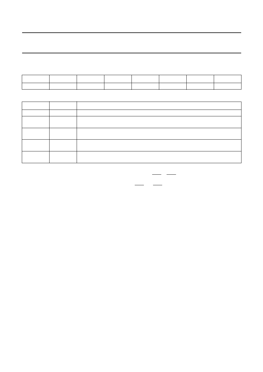
1.2
Memory
Table 1
ROM/RAM sizes
2
GENERAL DESCRIPTION
The P83C434 and P83C834 are low-cost microcontrollers
of the 80C51 family, with LCD drivers.
Main application is in the user-interface (keypad, display)
of consumer products, e.g. portable radios, CD-players,
etc.
This data sheet details the specific properties of the
P83C434 and P83C834. The shared characteristics of the
80C51 family of microcontrollers are described in
"Data
Handbook IC20", which should be read in conjunction with
this data sheet.
DEVICE
MEMORY
ROM
RAM
P83C434
4 kbytes
128 bytes
P83C834
8 kbytes
256 bytes
1
FEATURES
∑
80C51 type core
∑
System clock derived from an internal free running
Current Controlled Oscillator (CCO); no external
components required. Clock frequency can be adjusted
by software.
∑
Optimized for EMC (Electromagnetic Compatibility)
∑
Clock frequency f
clk
= 1 to 12 MHz
∑
12 I/O lines, quasi-bidirectional
∑
Gated interrupt on 8 I/O lines:
≠ P0.0 to P0.3 when LOW
≠ P0.4 to P0.7 when LOW or HIGH
∑
LCD driver clock, 32 kHz, which also provides the time
base for a Real Time Clock
∑
1-second interrupt by internal 15-bit counter
∑
On-chip Liquid Crystal Display (LCD) drivers with
26 outputs, comprising:
≠ 22, 23 or 24 segment drivers
≠ 1 to 4 backplanes
∑
LCD multiplexing rates: 1 : 1 (static), 1 : 2, 1 : 3 or 1 : 4
∑
Operating temperature:
-
40 to +85
∞
C
∑
Single power supply:
≠ Operating voltage: 3.5 to 5.5 V
≠ Power-down mode: 1.8 V.
1.1
Differences from the 80C51 core
∑
Port 0 quasi-bidirectional instead of open-drain.
∑
No external memory connection.
Signals EA, ALE and PSEN are not present.
∑
Port 1, Port 2 (pins P2.4 to P2.7) and Port 3 are not
present.
3
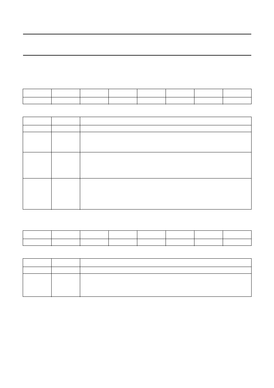
ORDERING INFORMATION
TYPE NUMBER
PACKAGE
TEMP.
RANGE (
∞
C)
NAME
DESCRIPTION
VERSION
P83C434CFP;
P83C834CFP
SDIP42 plastic shrink dual in-line package; 42 leads (600 mil)
SOT270-1
-
40 to +85
QFP44
plastic quad flat package; 44 leads (lead length 1.3 mm);
body 10
◊
10
◊
1.75 mm
SOT307-2
1997 Jul 03
4
Philips Semiconductors
Product specification
8-bit microcontrollers with LCD-driver
P83C434; P83C834
4
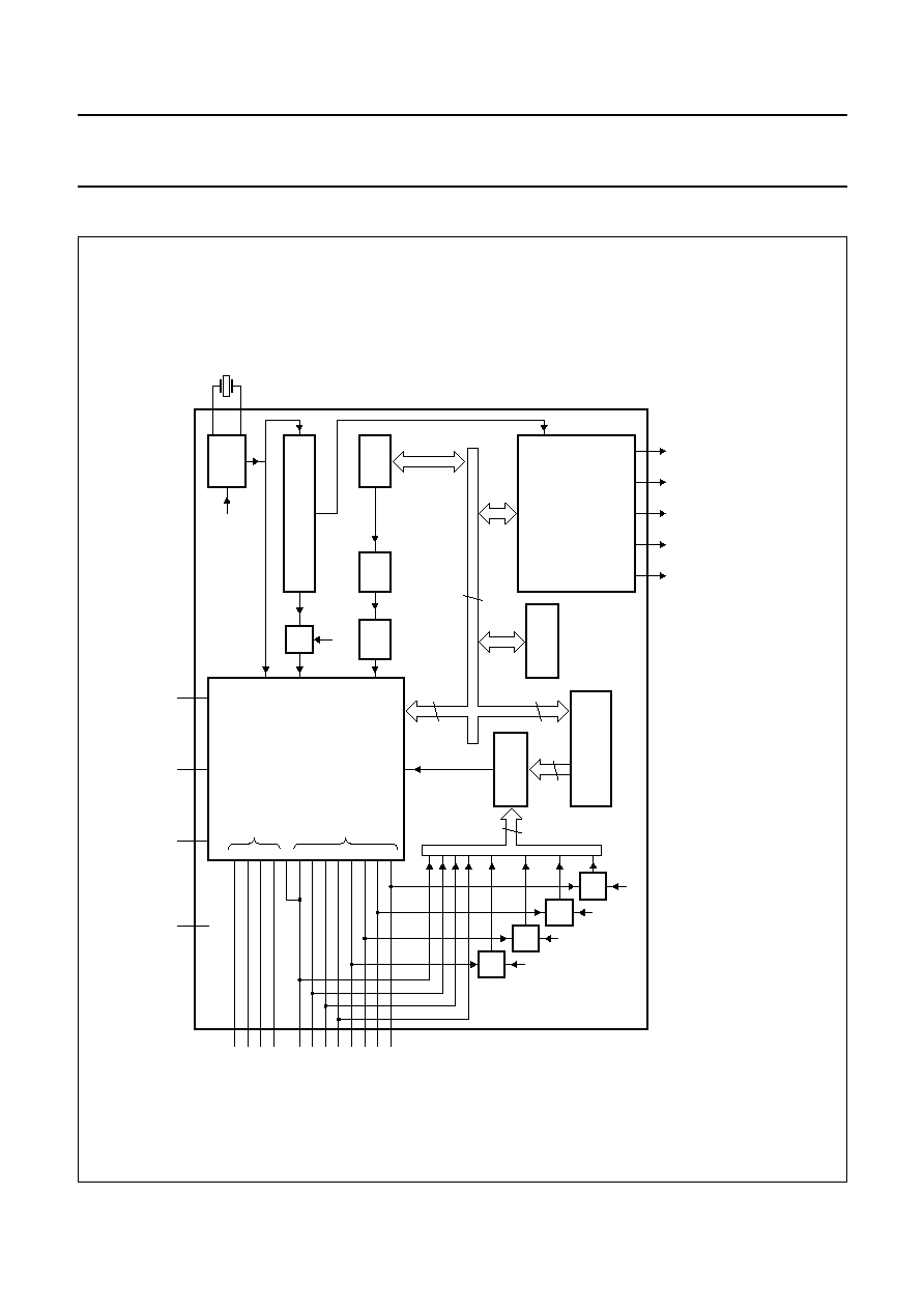
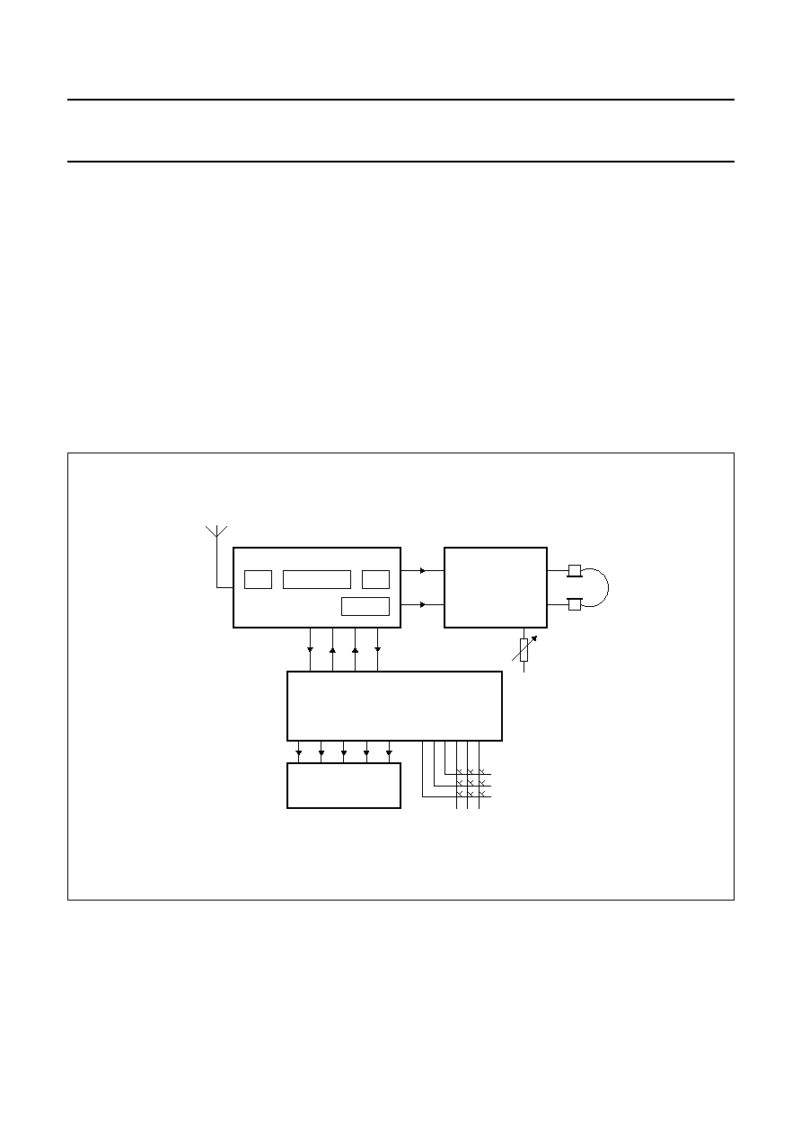
BLOCK DIAGRAM
handbook, full pagewidth
MGG012
80C51 CORE
RESET
T0
EI1
CLOCK
internal bus
EI0
P0.0 to P0.7
P0.7
P0.6
P0.5
P0.4
P0.3
P0.2
P0.1
P0.0
P2.3
P2.2
P2.1
P2.0
P2.0 to P2.3
V
DD(C)
V
SS
V
DD(P)
0
1
2
3
T1
0
1
2
3
4
5 6
7
8
8
MCON.0
MCON.1
MCON.2
MCON.3
INTERRUPT
GATES
8
INTERRUPT GATES
REGISTER (IG).
MCON
8
8
MCON.4
CCO
D/A
OSCON
LCD
UNIT
internal
CLOCK
BP0
BP1
S23/
BP2
S22/
BP3
S00
to
S21
1-SECOND COUNTER
OSC
32
kHz
MCON.5
XTAL1
XTAL2
(1)
Fig.1 Block diagram.
(1)
Drive lines S00 and S21 are not available with the SDIP42 (SOT270-1) package.
1997 Jul 03
5
Philips Semiconductors
Product specification
8-bit microcontrollers with LCD-driver
P83C434; P83C834
5
PINNING INFORMATION
5.1
Pinning
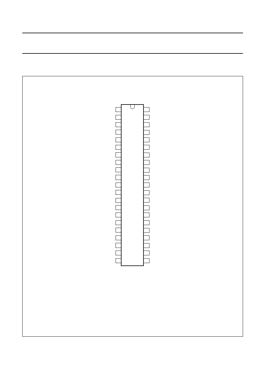
Fig.2 Pinning diagram for SDIP42 (SOT270-1).
handbook, halfpage
1
2
3
4
5
6
7
8
9
10
11
12
13
40
39
38
37
36
35
34
33
32
31
30
29
28
27
14
15
16
17
18
19
20
22
23
24
25
26
21
42
41
MGG011
P83C434
P83C834
P2.2
P2.3
RESET
SS
V
XTAL1
XTAL2
P0.0
P0.1
P0.2
S10
S11
S12
S13
S14
S15
S16
S09
S08
S07
S06
P0.3
P0.4
P0.5
P0.6
P0.7
S01
S02
S03
S04
S05
P2.1
P2.0
BP0
BP1
S23/BP2
S22/BP3
S20
S19
S18
S17
VDD(P)
VDD(C)
1997 Jul 03
6
Philips Semiconductors
Product specification
8-bit microcontrollers with LCD-driver
P83C434; P83C834
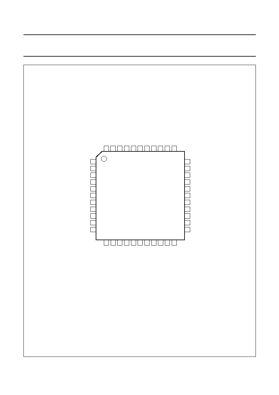
Fig.3 Pinning diagram for QFP44 (SOT307-2).
handbook, full pagewidth
1
2
3
4
5
6
7
8
9
10
11
33
32
31
30
29
28
27
26
25
24
23
12
13
14
15
16
17
18
19
20
21
22
44
43
42
41
40
39
38
37
36
35
34
MGG010
P83C434
P83C834
P2.2
P2.3
RESET
VDD(P)
VDD(C)
SS
V
XTAL1
XTAL2
P0.0
P0.1
P0.2
S10
S11
S12
S13
S14
S15
S16
S09
S08
S07
P06
P0.3
P0.4
P0.5
P0.6
P0.7
S00
S01
S02
S03
S04
S05
P2.1
P2.0
BP0
BP1
S23/BP2
S22/BP3
S21
S20
S19
S18
S17

1997 Jul 03
7
Philips Semiconductors
Product specification
8-bit microcontrollers with LCD-driver
P83C434; P83C834
5.2
Pin description
Table 2
Pin description for SDIP42 and QFP44
Notes
1. For proper V
DD
supply to V
DD(P)
and V
DD(C)
see Section 6.1.1.
2. In package SDIP42 (SOT270-1) segment drive lines S00 and S21 are not connected, so the total number of drive
lines is 22.
SYMBOL
PIN
DESCRIPTION
SDIP42
(SOT270-1)
QFP44
(SOT307-2)
S23/BP2
1
40
segment drive line 23/Backplane drive line 2
BP1
2
41
backplane drive line 1
BP0
3
42
backplane drive line 0
P2.0 to P2.3
4 to 7
43, 44, 1 and 2 quasi-bidirectional I/O line
RESET
8
3
reset input
V
DD(P)
9
4
power supply (+) for periphery and LCD unit; see note 1
V
SS
10
5
ground; double bonded
V
DD(C)
11
6
power supply for the core; see note 1
XTAL1
12
7
oscillator, XTAL connections
XTAL2
13
8
P0.0 to P0.7
14 to 21
9 to 16
Port 0: quasi-bidirectional I/O lines
S00
-
17
segment drive line 0; see note 2
S01 to S20
22 to 41
18 to 37
segment drive line 1 to 20
S21
-
38
segment drive line 21; see note 2
S22/BP3
42
39
segment drive line 22/Backplane drive line 3
1997 Jul 03
8
Philips Semiconductors
Product specification
8-bit microcontrollers with LCD-driver
P83C434; P83C834
6
FUNCTIONAL DESCRIPTION
The block diagram is shown in Fig.1. The P83C434 and
P83C834 provide all functions that are required for a user
interface. This is illustrated in the radio application detailed
in Chapter 12. In the following sections the functions of the
device are described.
6.1
Input/Output (I/O)
A total of 12 I/O lines are available.
Port 0 P0.0 to P0.7 (8 lines).
Port configuration: Quasi-bidirectional (push-pull in
emulation mode). For the Interrupt generation see
Fig.10. If one of the port lines P0.0 to P0.3 is a
logic 0 or one of the port lines P0.4 to P0.7 is equal
to the corresponding bit in the Miscellaneous
Control Register (MCON) and the corresponding bit
in the Interrupt Gate Register (IG) is a logic 1, then
an INT0 interrupt is generated.
Port 2 P2.0 to P2.3 (4 lines).
Port configuration: Quasi-bidirectional (push-pull in
emulation mode). When writing to Port 2, bits
P2.4 to P2.7 have to be fixed at HIGH. Data to be
written should be `1111
XXXX
B'.
6.1.1
EMC (E
LECTROMAGNETIC
C
OMPATIBILITY
)
In order to reduce EMI (Electromagnetic Interference) the
following design measures have been taken:
∑
Slope control is implemented on all the I/O lines.
Rise and fall time (10% to 90%) are:
20 ns < rise/fall time < 50 ns.
∑
The power supply and ground pins are placed next to
each other.
∑
Double bonding V
SS
pins, i.e. 2 bondpads for each pin.
∑
Limiting the drive capability of:
≠ clock drivers and prechargers.
≠ segment drivers and backplane drivers for the LCD.
∑
External decoupling of the of the CPU supply V
DD(C)
;
to avoid interference on the V
DD
line, the V
DD(C)
and
V
DD(P)
pins should be connected as illustrated in Fig.4.
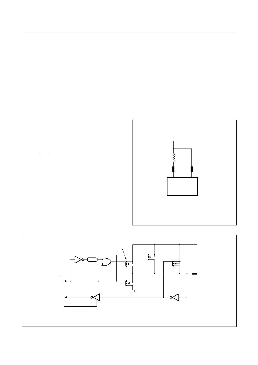
Fig.4 Avoiding interference on V
DD
.
handbook, halfpage
MGG019
P83C434
P83C834
VDD(C)
VDD
VDD(P)
2.2
µ
H
Fig.5 Standard output with switched pull-up current source.
handbook, full pagewidth
MLC926 - 1
p1
p2
p3
input data
read port pin
2 oscillator
periods
n
strong pull-up
I/O PIN
V
I1
Q
from port latch
INPUT
BUFFER
DD
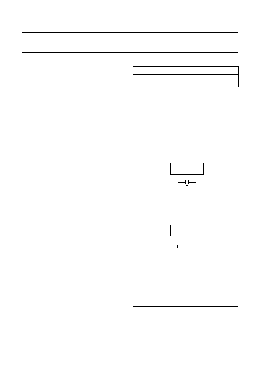
1997 Jul 03
9
Philips Semiconductors
Product specification
8-bit microcontrollers with LCD-driver
P83C434; P83C834
6.2
Oscillator
6.2.1
CPU
CLOCK
The internal timing circuits of the CPU are clocked by a
Current Controlled Oscillator (CCO). The oscillator is free
running and is adjusted by means of the Oscillator Control
Register (OSCON; see Section 6.6.4) and a
digital-to-analog converter; it does not require external
components. The frequency of the CPU clock can be
measured by means of Timer T0 which is clocked by the
32 kHz oscillator (see Section 6.2.2).
Adjustments can be made by changing the contents of the
OSCON register (see Fig.9). Over the range 0 to 31 the
frequency step size is constant (deviation
10%).
The frequency variation per step of the register is:
0.5 MHz < step size < 2 MHz.
At Power-on-reset the oscillator frequency will be:
1 MHz < f
OSC
< 4 MHz. Stability of the oscillator:
frequency change with time
1.5%. The maximum
operating frequency is:
12 MHz at V
DD
4.5 V.
The minimum operating frequency is 1 MHz.
In Power-down mode the oscillator is stopped.
6.2.2
LCD
DRIVER CLOCK
: 32
K
H
Z OSCILLATOR
A 32 kHz oscillator provides the clocking of the LCD timing
generator and may also be used as the time base for a
Real Time Clock. The output of the 32 kHz oscillator is also
used as an input of Timer/Counter 0.
The frequency of the 32 kHz oscillator need not be exactly
32 kHz, and is determined by the component(s) connected
between pins XTAL1 and XTAL2. See Chapter 11.
The oscillator is suitable for use with either:
∑
A crystal; connected as shown in Fig.6a
∑
External drive; connected as shown in Fig.6b.
During Power-down mode, the control bit RUN32 in the
Miscellaneous Control Register (MCON) determines
whether the oscillator is stopped or running continuously;
see Table 3.
The output of the oscillator (XTAL2) is used as an input to
the Timer/Counter 0. This can be useful for accurate time
measurements and generation of time-slots. For example
it may be used to determine (and possibly adjust) the
frequency of the CCO that is used for the CPU clock.
Table 3
Oscillator status during Power-down mode
6.2.3
15-
BIT COUNTER
(1-
SECOND
T
IMER
)
An interrupt is generated every second by the 15-bit
counter. This 1-second timer is a 15-bit counter, clocked
by the 32 kHz oscillator output. When this counter
overflows it generates an INT1 interrupt by setting SECINT
in the Miscellaneous Control Register (MCON). Reset of
this interrupt is carried out via software by clearing bit
SECINT.
RUN32
32 kHz OSCILLATOR
HIGH
running
LOW
stopped
handbook, halfpage
MLC928
XTAL1
XTAL2
Fig.6 Oscillator configurations P83C434/P83C834.
handbook, halfpage
MBE312
XTAL1
XTAL2
n.c.
external clock
(not TTL compatible)
a. Crystal oscillator.
b. External clock drive.
1997 Jul 03
10
Philips Semiconductors
Product specification
8-bit microcontrollers with LCD-driver
P83C434; P83C834
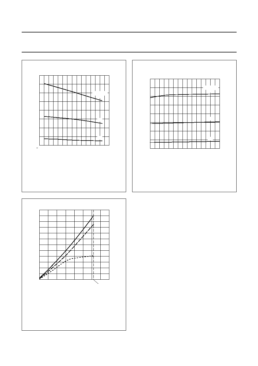
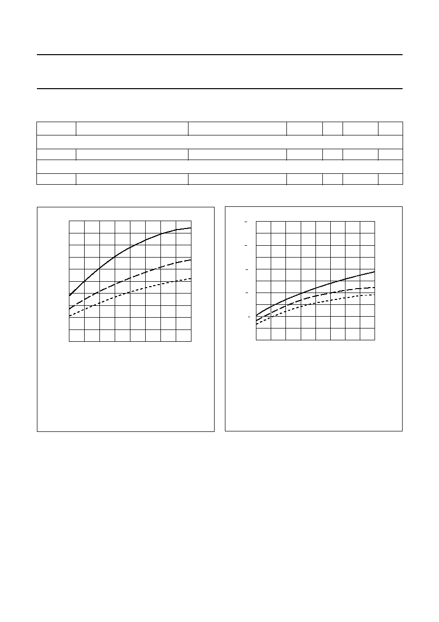
Fig.7
f
osc
as function of temperature;
at V
DD
= 5 V.
handbook, halfpage
0
50
0
100
16
12
4
8
MBE313
50
T ( C)
o
f osc
(MHz)
OSCON =
FH
7H
1H
Fig.8 f
osc
as function of V
DD
.
handbook, halfpage
0
2
3
5
16
12
4
8
MBE314
4
V (V)
f osc
(MHz)
OSCON =
FH
7H
1H
DD
Fig.9 f
osc
as function of OSCON.
handbook, halfpage
0
10
20
40
36
0
12
24
MBE315
30
31(max)
fosc
(MHz)
contents of OSCON (decimal)
(1)
(2)
(3)
(1) Fast case; V
DD
= 5.5 V, T
amb
=
-
40
∞
C.
(2) Typical case; V
DD
= 4.0 V, T
amb
= 25
∞
C.
(3) Slow case; V
DD
= 2.0 V, T
amb
= 85
∞
C.
1997 Jul 03
11
Philips Semiconductors
Product specification
8-bit microcontrollers with LCD-driver
P83C434; P83C834
6.3
Interrupts
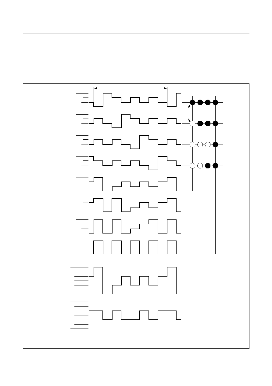
The P83C434 and P83C834 have 4 interrupt sources;
these are shown Fig.10.
Interrupt INT0 is generated when one of the I/O lines
(P0.0 to P0.3) becomes LOW; or one of I/O lines
(P0.4 to P0.7) equals the corresponding bit in the MCON
register (ILVL0 to ILVL3). By means of bit IT0 in the TCON
register this interrupt can be chosen to be:
∑
Level sensitive, when IT0 = LOW; INT0 must be inactive
before a return from interrupt is given, otherwise the
same interrupt will occur again.
∑
Edge sensitive, when IT0 = HIGH; the internal hardware
will reset the latch when the LCALL is executed for the
vector address (see Table 7).
Interrupt INT1 is generated by the overflow of the 1-second
counter. The overflow signal is latched. The output of the
latch will set the SECINT bit in the MCON register.
When SECINT is set the overflow latch will be reset.
Interrupt INT1 is selected as edge or level sensitive by the
state of the IT1 bit in the TCON register. However, it is
recommended to always set IT1 to HIGH (edge sensitive)
so that IE1 will be reset by the internal hardware when the
LCALL is executed for the vector address.
In the interrupt routine SECINT should be reset by
software so that with the next 1-second overflow another
interrupt may be generated.
Timer 0 and Timer 1 interrupts are generated by TF0 and
TF1 which are set by an overflow of their respective
Timer/Counter registers (except for Timer 0 in mode 3;
see
"Data Handbook IC20, 80C51 Family, Chapter
Timer/Counters"). When a timer interrupt is generated, the
flag that generated it is cleared by the internal hardware
when the LCALL is executed for the vector address.
All of the bits that generate interrupts can be set or cleared
by software, with the same result as though it had been set
or cleared by hardware. That is, interrupts can be
generated or pending interrupts can be cancelled in
software.
Each of these interrupts sources can be individually
enabled or disabled by setting or clearing the bit in Special
Function Register IE (see Table 5). IE also contains a
global disable bit EA, which disables all interrupts at once.
6.3.1
I
NTERRUPT
E
NABLE
R
EGISTER
(IE)
Table 4
Interrupt Enable Register (address A8H)
Table 5
Description of IE bits
7
6
5
4
3
2
1
0
EA
-
-
-
ET1
EX1
ET0
EX0
BIT
SYMBOL
DESCRIPTION
7
EA
Disable all interrupts. If EA is:
LOW, then no interrupt will be acknowledged.
HIGH, then each interrupt source is individually enabled or disabled by setting or
clearing its enable bit.
6 to 4
-
Reserved.
3
ET1
Enables or disables the Timer 1 Overflow Interrupt. If ET1 is LOW then the Timer 1
interrupt is disabled.
2
EX1
Enables or disables the External Interrupt 1. If EX1 is LOW then the External 1
interrupt is disabled.
1
ET0
Enables or disables the Timer 0 Overflow Interrupt. If ET0 is LOW then the Timer 0
interrupt is disabled.
0
EX0
Enables or disables the External Interrupt 0. If EX0 is LOW then the External 0
interrupt is disabled.

1997 Jul 03
12
Philips Semiconductors
Product specification
8-bit microcontrollers with LCD-driver
P83C434; P83C834
handbook, full pagewidth
MLC919 - 1
TF0
IE0
IE0¥
TF0
IT0
'0'
'1'
'0'
'1'
INT0
interupt
sources
1
2
3
4
5
6
7
8
1
2
3
1
2
3
1
2
3
1
2
3
MCON: ILVL0 to ILVL3
interrupt
gates
P0.0
P0.1
P0.2
P0.3
P0.4
P0.5
P0.6
P0.7
Timer 0 overflow
TF1
TF1
Timer 1 overflow
1-sec counter
overflow
9
1
2
3
IE1
IE1¥
IT1
INT1
SECINT
LATCH
1
2
3
1
2
3
Fig.10 Interrupt sources.
1997 Jul 03
13
Philips Semiconductors
Product specification
8-bit microcontrollers with LCD-driver
P83C434; P83C834
6.3.2
P
RIORITY LEVEL STRUCTURE
The priority level of each interrupt source can be
individually programmed by setting or clearing a bit in the
Interrupt Priority Register (IP; see Section 6.3.4). A low
priority interrupt can itself be interrupted by a high priority
interrupt, but not by another low priority interrupt. A high
priority interrupt can not be interrupted by another interrupt
source.
If two requests of different priority levels are received
simultaneously, the request of higher priority level is
serviced. If request of the same priority level is received
simultaneously, an internal polling sequence determines
which request is serviced. Thus, within each priority level
there is a second priority structure determined as shown in
Table 6.
The IP register contains a number of not implemented bits.
IP.7, IP.6 and IP.5 are reserved in the 80C51.
User software should not write logic 1's to these positions,
since they may be used in other 8051-Family products.
Table 6
Priority within levels
Note
1. The `Priority within level' structure is only used to
resolve simultaneous requests of the same priority
level.
6.3.3
H
OW
I
NTERRUPTS ARE HANDLED
The interrupt flags are sampled at S5P2 of every machine
cycle. The samples are polled during the following
machine cycle. If one of the flags was in a set condition at
S5P2 of the preceding cycle, the polling cycle will find it
and the interrupt system will generate an LCALL to the
appropriate service routine, provided this hardware
generated LCALL is not blocked by any of the following
conditions:
1. An interrupt of equal priority or higher priority level is
already in progress.
2. The current (polling) cycle is not the final cycle in the
execution of the instruction in progress.
3. The instruction in progress is RETI or any write to the
IE or IP registers.
SOURCE
PRIORITY WITHIN LEVEL
(1)
IE0
1 (highest)
TF0
2
IE1
3
TF1
4 (lowest)
Condition 2 ensures that the instruction in progress will be
completed before vectoring to any service routine.
Condition 3 ensures that if the instruction in progress is
RETI or any access to IE or IP, then at least one more
instruction will be executed before the interrupt is vectored
to.
The polling cycle is repeated with each machine cycle, and
the values polled are the values that were present at S5P2
of the previous machine cycle. Note that if an interrupt flag
is active but not being responded to for one of the above
mentioned conditions, if the flag is still inactive when the
blocking condition is removed, the denied interrupt will not
be serviced. In other words, the fact that the interrupt flag
was once active but not serviced is not remembered.
Every polling cycle is new.
The polling cycle/LCALL sequence is illustrated in
"Data Handbook IC20, 80C51 Family, Fig.20".
Note that if an interrupt of higher priority level becomes
active prior to S5P2 of the machine cycle labelled C3
("Data Handbook IC20, 80C51 Family, Fig.20"), then in
accordance with the above rules it will be vectored to
during C5 and C6, without any instruction of the lower
priority routine having been executed. Thus the processor
acknowledges an interrupt request by executing a
hardware generated LCALL to the appropriate servicing
routine. The hardware generated LCALL pushes the
contents of the Program Counter on to the stack (but it
does not save the PSW) and reloads the PC with an
address that depends on the source of the interrupt being
vectored to as shown in Table 7.
Execution proceeds from that location until the RETI
instruction is encountered. The RETI instruction informs
the processor that the interrupt routine is no longer in
progress, then pops the top two bytes from the stack and
reloads the Program Counter. Execution of the interrupted
program continues from where it left off.
Note that a simple RET instruction would also return
execution to the interrupted program, but it would have left
the interrupt control system thinking an interrupt was still in
progress, making future interrupts impossible.
Table 7
Vector addresses
SOURCE
VECTOR ADDRESS
IE0
0003H
TF0
000BH
IE1
0013H
TF1
001BH
1997 Jul 03
14
Philips Semiconductors
Product specification
8-bit microcontrollers with LCD-driver
P83C434; P83C834
6.3.4
I
NTERRUPT
P
RIORITY
R
EGISTER
(IP)
Table 8
Interrupt Priority Register (address B8H)
Table 9
Description of IP bits
7
6
5
4
3
2
1
0
-
-
-
-
PT1
PX1
PT0
PX0
BIT
SYMBOL
DESCRIPTION
7 to 4
-
Reserved.
3
PT1
Defines the Timer 1 Overflow Interrupt priority level. When PT1 is HIGH, Timer 1
Overflow Interrupt is assigned a high priority level.
2
PX1
Defines the External Interrupt 1 priority level. When PX1 is HIGH, External
Interrupt 1 is assigned a high priority level.
1
PT0
Defines the Timer 0 Overflow Interrupt priority level. When PT0 is HIGH, Timer 0
Overflow Interrupt is assigned a high priority level.
0
PX0
Defines the External Interrupt 0 priority level. When PX0 is HIGH, External
Interrupt 0 is assigned a high priority level.
6.4
Reduced power modes
6.4.1
I
DLE MODE
In the Idle mode, the CPU puts itself to sleep while all of
the on-chip peripherals remain active. The instruction to
invoke the Idle mode is the last instruction executed in the
normal operating mode before the Idle mode is activated.
The CPU contents, the on-chip RAM, and all of the special
function registers remain intact during this mode. The Idle
mode can be terminated either by any enabled interrupt (at
which time the process is picked up at the interrupt service
routine and continued), or by a hardware reset which starts
the processor in the same manner as a power-on reset.
6.4.2
P
OWER-DOWN MODE
In the Power-down mode, the CCO oscillator (processor
clock) is stopped; as the instruction to invoke Power-down
mode is the last instruction executed. Whether the 32 kHz
oscillator is stopped depends on bit RUN32 in the MCON
register (MCON5). The Power-down mode can be
terminated by a RESET in same way as in the 80C51 or in
addition by one of two external interrupts, INT0 or INT1.
A termination with an external interrupt does not affect the
internal data memory and does not affect the Special
Function Registers. This makes it possible to exit
Power-down without changing the port output levels.
To terminate the Power-down mode with an external
interrupt, INT0 or INT1 must be switched to level-sensitive
and must be enabled. The external interrupt input signal
INT0 and INT1 must be kept LOW until the oscillator has
restarted and stabilized. An instruction following the
instruction that puts the device in the Power-down mode
will be executed. The control bits for the reduced power
modes are in the Special Function Register PCON.
To wake-up the microcontroller by a reset, the RESET pin
must be kept HIGH for a minimum of 36
µ
s.
6.5
Reset
Reset is accomplished either at power-on when the supply
voltage rises above Power-on-reset threshold or by a
logic 1 signal at the RESET pin.
The Power-on-reset threshold is minimum 1.8 V and
maximum 3.0 V. The RESET signal should be active
(HIGH) for at least 2 machine cycles (24 oscillator
periods).
The reset algorithm puts registers and flip-flops in a
defined state (see 80C51 Family specification in
"Data
Handbook IC20" and Section 6.6.1). The I/O ports are set
to a logic 1 at reset.
To wake-up from power-down the RESET signal must be
kept HIGH for a minimum of 36
µ
s.

1997 Jul 03
15
Philips Semiconductors
Product specification
8-bit microcontrollers with LCD-driver
P83C434; P83C834
6.6
Special Function Registers (SFRs)
6.6.1
C
HANGES W
.
R
.
T
. 80C51
KERNEL
∑
Removed SFRs: P3, P1, SCON and SBUF
∑
Added SFRs: IG, MCON, OSCON, LCDCON and LCD0 to LCD11.
Table 10 Overview of the additional SFRs
All SFRs are Read/Write registers.
6.6.2
I
NTERRUPT
G
ATE
R
EGISTER
(IG)
Table 11 Interrupt Gate Register (address 97H)
Table 12 Description of IG bits
REGISTER
DESCRIPTION
ADDRESS
RESET VALUE
IG
Interrupt Gate Register
97H
00H
MCON
Miscellaneous Control Register
98H
00H
OSCON
Oscillator Control Register
B7H
01H
LCDCON
LCD Control Register
B9H
0CH
LCD0 to LCD5
LCD segment display registers
9AH to 9FH
00H
LCD6 to LCD11
BAH to BFH
00H
7
6
5
4
3
2
1
0
IG.7
IG.6
IG.5
IG.4
IG.3
IG.2
IG.1
IG.0
BIT
SYMBOL
DESCRIPTION
7 to 0
IG.7 to IG.0
gate signals for interrupt from I/O lines P0.7 to P0.0. If signal IG.n is:
LOW, then no interrupt is possible
HIGH, then interrupt is possible
1997 Jul 03
16
Philips Semiconductors
Product specification
8-bit microcontrollers with LCD-driver
P83C434; P83C834
6.6.3
M
ISCELLANEOUS
C
ONTROL
R
EGISTER
(MCON)
This register is bit-addressable.
Table 13 Miscellaneous Control Register (address 98H)
Table 14 Description of MCON bits
6.6.4
O
SCILLATOR
C
ONTROL
R
EGISTER
(OSCON)
Table 15 Oscillator Control Register (address B7H)
Table 16 Description of OSCON bits
7
6
5
4
3
2
1
0
-
-
RUN32
SECINT
ILVL3
ILVL2
ILVL1
ILVL0
BIT
SYMBOL
DESCRIPTION
7 and 6
-
Reserved.
5
RUN32
Prevent stop of 32 kHz oscillator in Power-down mode. If RUN32 is:
HIGH, then the 32 kHz oscillator is not stopped in Power-down mode.
LOW, then the 32 kHz oscillator is stopped in Power-down mode.
4
SECINT
1-second interrupt flag. Is set by hardware on overflow of the 1-second counter.
Can be Set/Reset via software. If SECINT is:
HIGH, then there is an interrupt on overflow.
LOW, then there is no interrupt on overflow.
3 to 0
ILVL3
to
ILVL0
The state of these bits determine the signal level of the inputs P0.m (m = 4 to 7) which
will generate the interrupt EI0 (dependent on bits IG.4 to IG.7 respectively).
If ILVLn (n = 0 to 3) is:
LOW, then P0.m = LOW, will cause an interrupt.
HIGH, then P0.m = HIGH, will cause an interrupt.
7
6
5
4
3
2
1
0
-
-
-
OSCON.4
OSCON.3
OSCON.2
OSCON.1
OSCON.0
BIT
SYMBOL
DESCRIPTION
7 to 5
-
Reserved.
4 to 0
OSCON.4
to
OSCON.0
These 5 bits can hold a decimal value in the range of 0 to 31, that will be converted to a
current that controls the frequency of the CCO of the CPU clock; can be set by software.
The register value is converted to an analog current that controls the oscillator
(see Section 6.2.1).

1997 Jul 03
17
Philips Semiconductors
Product specification
8-bit microcontrollers with LCD-driver
P83C434; P83C834
6.6.5
LCD C
ONTROL
R
EGISTER
(LCDCON)
After an external or Power-on-reset the LCD Control Register holds the value 0CH (see Table 10) resulting in:
∑
The LCD is disabled. All segment and backplane drivers are set to the V
SS
level.
∑
BIAS is set to generate
1
/
3
V
DD(P)
.
∑
Bits MD0 and MD1 reset the multiplex ratio to the 1 : 4 mode.
Table 17 LCD Control Register (address B9H)
Table 18 Description of LCDCON bits
Table 19 Multiplex ratio mode selection
6.6.6
LCD
SEGMENT DISPLAY REGISTERS
(LCD0
TO
LCD11)
The 12 display registers, LCD0 to LCD11, are 8-bit derivative (Read/Write) registers which store LCD segment data.
For detailed information, regarding the LCD0 to LCD11, see Table 23 in Section 6.7.7.
7
6
5
4
3
2
1
0
-
-
-
-
MD1
MD0
BIAS
ENLCD
BIT
SYMBOL
DESCRIPTION
7 to 4
-
Reserved.
3
MD1
Mode bits. MD0 and MD1 determine the multiplex rate; see Table 19.
2
MD0
1
BIAS
The BIAS bit sets the LCD voltage bias generator. If BIAS is:
HIGH, then the LCD voltage bias generator is set to
1
/
2
V
DD(P)
.
LOW, then the LCD voltage bias generator is set to
1
/
3
V
DD(P)
.
0
ENLCD
Enable LCD. If ENLCD is:
LOW, then the LCD is disabled.
All segment and backplane drivers are set to the V
SS
level.
HIGH, then the LCD is enabled and character display is possible.
MD1
MD0
MULTIPLEX RATIO MODE
0
0
static
0
1
1 : 2
1
0
1 : 3
1
1
1 : 4
1997 Jul 03
18
Philips Semiconductors
Product specification
8-bit microcontrollers with LCD-driver
P83C434; P83C834
6.7
LCD driver unit
The LCD driver unit has 24 segment drivers, two of which
can also serve as backplane drivers. Selection will be done
automatically, depending on the multiplex ratio as shown
in Table 20.
6.7.1
F
UNCTIONAL DESCRIPTION OF THE
LCD
DRIVER
The P83C434 and P83C834 have a display driver which
interfaces to almost any LCD which has a low multiplex
rate. The interface delivers drive signals for any static or
multiplexed LCD panel that contains up to 4 backplanes
and up to 24 segments. Figure 11 shows the block
diagram of the LCD driver. The following features are
incorporated:
∑
Selection of backplane drive configuration:
≠ static
≠ 2, 3 or 4 backplane multiplexing
∑
Selection of display bias configuration:
≠
1
/
2
internal LCD bias generation
≠
1
/
3
internal LCD bias generation
∑
24 individual segment drivers can be used to provide:
≠ up to twelve 7-segment numeric characters
≠ up to six 14-segment alphanumeric characters
≠ graphic using up to 88 elements
≠ twelve 8-bit derivative registers for display data bits.
The display configurations possible with the P83C434 and
P83C834 depend on the number of active backplane
outputs required.
A selection of display configurations is given in Table 21.
The appropriate biasing voltages for the multiplexed LCD
wave forms are generated internally.
At power-on all the LCD driver control register bits are
cleared. The LCD driver is not affected by executing Idle or
Power-down modes.
6.7.2
LCD
BIAS GENERATION
The LCD operating voltage: V
op
= V
DD(P)
-
V
SS
.
V
op
should be chosen so that the off voltage (V
off(rms)
) is
just below the threshold voltage (V
th
), typically when the
LCD exhibits 10% contrast. Fractional LCD biasing
voltages are obtained from an internal voltage divider of
three resistors connected between V
SS
and V
DD(P)
. The
centre resistor may be switched out of circuit to provide a
1
/
2
bias voltage level for a 1 : 2 multiplex configuration.
6.7.3
LCD
VOLTAGE SELECTOR
The LCD voltage selector coordinates the multiplexing of
the LCD according to the selected drive configuration.
The operation of the voltage selector is controlled by the
MODE bits in the LCD control byte.
The biasing configurations that apply to the preferred
mode of operation, together with the biasing
characteristics as functions of V
op
= V
DD(P)
-
V
SS
and the
resulting discrimination ratios (D), are given in Table 22.
Fig.11 Block diagram of the LCD driver.
handbook, full pagewidth
MGG013
LCD VOLTAGE SELECTOR
SEGMENT
REGISTERS
LCD CONTROL
REGISTER
SEGMENT
BACKPLANE
MUX.
LCD BIAS
GENERATION
LCD DRIVERS
22
24
4
8
internal
bus
CLOCK
VDD(P)
VSS
S0 to S21 S22/BP3 S23/BP2 BP1 BP0
1997 Jul 03
19
Philips Semiconductors
Product specification
8-bit microcontrollers with LCD-driver
P83C434; P83C834
Table 20 Mode selection Segments/Backplanes
Table 21 Selection of display configurations
Table 22 LCD drive modes and characteristics
Note
1. Multiplex drive ratios of 1 : 3 and 1 : 4 with
1
/
2
bias are possible, but the discrimination contrast ratios are reduced;
for 1 : 3, D = 1.732 and for 1 : 4, D = 1.528. However, there is an advantage that leads to reduction of V
op
as follows:
a) for 1 : 3 multiplex (
1
/
2
bias), V
op
= 2.449
◊
V
off(rms)
.
b) For 1 : 4 multiplex (
1
/
2
bias), V
op
= 2.309
◊
V
off(rms)
.
This compared to V
op
= 3
◊
V
off(rms)
when
1
/
3
bias is used.
MULTIPLEX RATIO
SEGMENTS
BACKPLANES
1 : 1 (static)
S00 to S21, S22/BP3, S23/BP2
BP0
1 : 2
S00 to S21, S22/BP3, S23/BP2
BP0, BP1
1 : 3
S00 to S21, S22/BP3
BP0, BP1, S23BP2
1 : 4
S00 to S21
BP0, BP1, S23/BP2, S22/BP3
NUMBER OF
7-SEGMENTS NUMERIC
14-SEGMENTS
ALPHANUMERIC
DOT MATRIX
BACKPLANES SEGMENTS
DIGITS
INDICATOR
SYMBOLS
CHARACTERS
INDICATOR
SYMBOLS
4
88
12
4
6
4
88 dots (4
◊
22)
3
69
9
6
4
13
69 dots (3
◊
23)
2
48
6
6
3
6
48 dots (2
◊
24)
1
24
3
3
1
10
24 dots (1
◊
24)
LCD DRIVE MODE
NUMBER OF
LCD BIAS
CONFIGURATION
BACKPLANES
LEVELS
static
1
2
static
0
1
1 : 2
2
3
1
/
2
0.354
0.791
2.236
1 : 2
2
4
1
/
3
0.333
0.745
2.236
1 : 3
(1)
3
4
1
/
3
0.333
0.638
1.915
1 : 4
(1)
4
4
1
/
3
0.333
0.577
1.7321
V
off(rms)
V
op
---------------------
V
on(rms)
V
op
---------------------
D
V
on(rms)
V
off(rms)
---------------------
=
1997 Jul 03
20
Philips Semiconductors
Product specification
8-bit microcontrollers with LCD-driver
P83C434; P83C834
6.7.4
LCD
DRIVE MODE WAVEFORMS
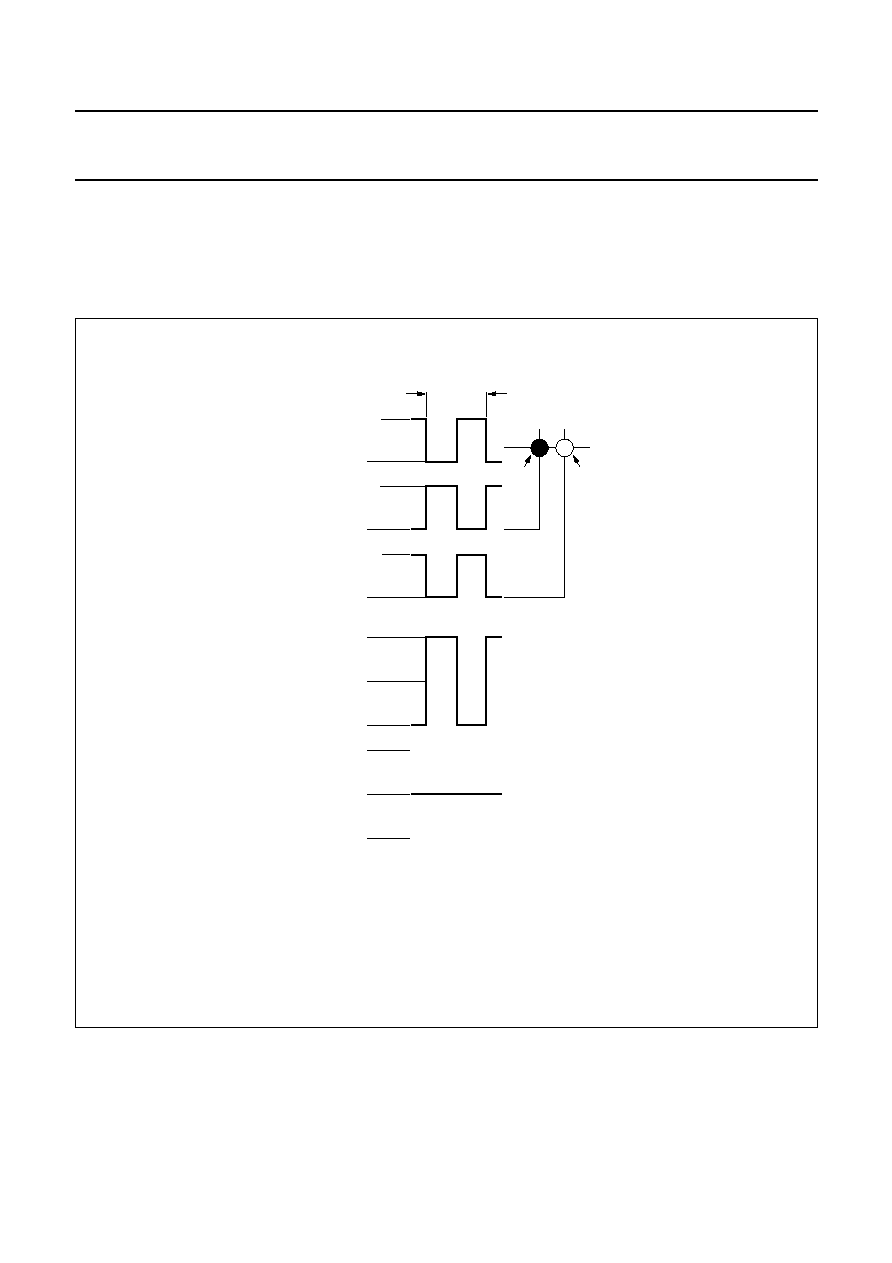
6.7.4.1
Static drive mode
The static LCD drive mode is used when a single backplane is provided in the LCD. Backplane and segment drive
waveforms are shown in Fig.12.
handbook, full pagewidth
MGG014
VDD(P)
VDD(P)
VDD(P)
VSS
VSS
VSS
Vop
Vop
-
Vop
-
Vop
state 1
0
BP0
Sn
+
1
Sn
state 2
0
(a) waveforms at driver
(b) resultant waveforms
at LCD element
LCD elements
state 1
(on)
state 2
(off)
Tframe
Fig.12 Static drive mode waveforms (V
op
= V
DD(P)
-
V
SS
).
V
state1
t
( )
V
S
n
t
( )
V
BP0
t
( )
≠
=
V
on(rms)
V
op
=
V
state2
t
( )
V
S
n
1
+
t
( )
V
BP0
t
( )
≠
=
V
off(rms)
0 V
=
1997 Jul 03
21
Philips Semiconductors
Product specification
8-bit microcontrollers with LCD-driver
P83C434; P83C834
6.7.4.2
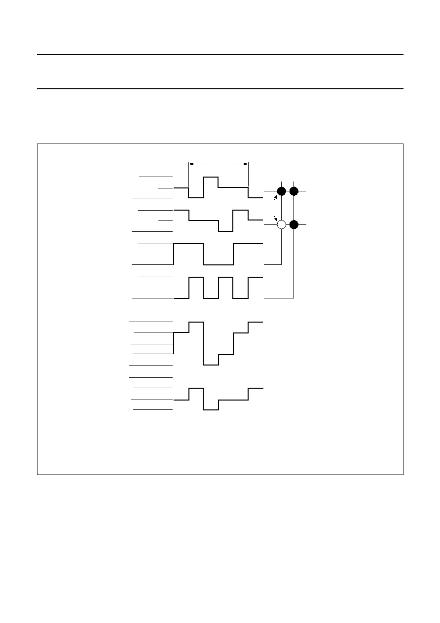
1 : 2 multiplex drive mode
When two backplanes are provided in the LCD, the 1 : 2 multiplex mode applies. The P83C434; P83C834 allows use of
1
/
2
or
1
/
3
bias in this mode as shown in Figs 13 and 14.
full pagewidth
MGG015
state 1
0
BP0
(a) waveforms at driver
(b) resultant waveforms
at LCD element
LCD elements
state 2
Tframe
BP1
-
Vop/2
-
Vop
Vop/2
Vop
-
Vop/2
-
Vop
Vop/2
Vop
state 2
0
state 1
VDD(P)
VDD(P)
VDD(P)
(VDD(P)+VSS)/2
VDD(P)
(VDD(P)+VSS)/2
VSS
VSS
VSS
VSS
Sn
+
1
Sn
Fig.13 Waveforms for the 1 : 2 multiplex mode with
1
/
2
bias (V
op
= V
DD(P)
-
V
SS
).
V
state1
t
( )
V
S
n
t
( )
V
BP0
t
( )
≠
=
V
on(rms)
0.791V
op
=
V
state2
t
( )
V
S
n
t
( )
V
BP0
t
( )
≠
=
V
off(rms)
0.354V
op
=
1997 Jul 03
22
Philips Semiconductors
Product specification
8-bit microcontrollers with LCD-driver
P83C434; P83C834
agewidth
MGG016
state 1
0
BP0
(a) waveforms at driver
(b) resultant waveforms
at LCD element
LCD elements
state 2
BP1
Sn
state 1
state 2
Tframe
-
Vop
Vop/3
-
Vop/3
2Vop/3
-
2Vop/3
Vop
0
-
Vop
Vop/3
-
Vop/3
2Vop/3
-
2Vop/3
Vop
VDD(P)
VSS
VSS
+
Vop/3
VSS
+
2Vop/3
VDD(P)
VSS
VSS
+
Vop/3
VSS
+
2Vop/3
VDD(P)
VSS
VSS
+
Vop/3
VSS
+
2Vop/3
VDD(P)
VSS
VSS
+
Vop/3
VSS
+
2Vop/3
Sn
+
1
Fig.14 Waveforms for the 1 : 2 multiplex mode with
1
/
3
bias (V
op
= V
DD(P)
-
V
SS
).
V
state1
t
( )
V
S
n
t
( )
V
BP0
t
( )
≠
=
V
on(rms)
0.745V
op
=
V
state2
t
( )
V
S
n
t
( )
V
BP0
t
( )
≠
=
V
off(rms)
0.333V
op
=
1997 Jul 03
23
Philips Semiconductors
Product specification
8-bit microcontrollers with LCD-driver
P83C434; P83C834
6.7.4.3
1 : 3 multiplex drive mode
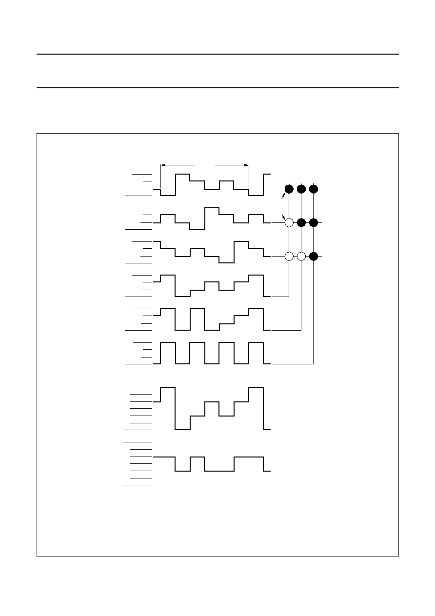
When three backplanes are provided in the LCD, the 1 : 3 multiplex mode applies, as shown in Fig.15.
book, full pagewidth
MGG017
state 1
0
BP0
(b) resultant waveforms
at LCD element
LCD elements
state 2
BP1
state 1
state 2
0
(a) waveforms at driver
BP2/S23
Tframe
-
Vop
Vop/3
-
Vop/3
2Vop/3
-
2Vop/3
Vop
-
Vop
Vop/3
-
Vop/3
2Vop/3
-
2Vop/3
Vop
VDD(P)
VSS
VSS
+
Vop/3
VSS
+
2Vop/3
VDD(P)
VSS
VSS
+
Vop/3
VSS
+
2Vop/3
VDD(P)
VSS
VSS
+
Vop/3
VSS
+
2Vop/3
VDD(P)
VSS
VSS
+
Vop/3
VSS
+
2Vop/3
VDD(P)
VSS
VSS
+
Vop/3
VSS
+
2Vop/3
VDD(P)
VSS
VSS
+
Vop/3
VSS
+
2Vop/3
Sn
+
1
Sn
+
2
Sn
Fig.15 Waveforms for the 1 : 3 multiplex drive mode (V
op
= V
DD(P)
-
V
SS
).
V
state1
t
( )
V
S
n
t
( )
V
BP0
t
( )
≠
=
V
on(rms)
0.638V
op
=
V
state2
t
( )
V
S
n
t
( )
V
BP0
t
( )
≠
=
V
off(rms)
0.333V
op
=
1997 Jul 03
24
Philips Semiconductors
Product specification
8-bit microcontrollers with LCD-driver
P83C434; P83C834
6.7.4.4
1 : 4 multiplex drive mode
When four backplanes are provided in the LCD, the 1 : 4 multiplex mode applies, as shown in Fig.16.
handbook, full pagewidth
MGG018
state 1
0
BP0
(b) resultant waveforms
at LCD element
LCD elements
state 2
BP1
state 1
state 2
0
BP2/S23
(a) waveforms at driver
BP3/S22
Tframe
-
Vop
Vop/3
-
Vop/3
2Vop/3
-
2Vop/3
Vop
-
Vop
Vop/3
-
Vop/3
2Vop/3
-
2Vop/3
Vop
VDD(P)
VSS
VSS
+
Vop/3
VSS
+
2Vop/3
VDD(P)
VSS
VSS
+
Vop/3
VSS
+
2Vop/3
VDD(P)
VSS
VSS
+
Vop/3
VSS
+
2Vop/3
VDD(P)
VSS
VSS
+
Vop/3
VSS
+
2Vop/3
VDD(P)
VSS
VSS
+
Vop/3
VSS
+
2Vop/3
VDD(P)
VSS
VSS
+
Vop/3
VSS
+
2Vop/3
VDD(P)
VSS
VSS
+
Vop/3
VSS
+
2Vop/3
VDD(P)
VSS
VSS
+
Vop/3
VSS
+
2Vop/3
Sn
+
1
Sn
+
2
Sn
+
3
Sn
Fig.16 Waveforms for the 1 : 4 multiplex drive mode (V
op
= V
DD(P)
-
V
SS
).
V
state1
t
( )
V
S
n
t
( )
V
BP0
t
( )
≠
=
V
on(rms)
0.577V
op
=
V
state2
t
( )
V
S
n
t
( )
V
BP0
t
( )
≠
=
V
off(rms)
0.333V
op
=
1997 Jul 03
25
Philips Semiconductors
Product specification
8-bit microcontrollers with LCD-driver
P83C434; P83C834
6.7.5
LCD
SEGMENT DRIVER OUTPUTS
The LCD drive section includes 24 segment outputs
(S00 to S23) which should be connected directly to the
LCD. The segment data bits are multiplexed to the outputs
in accordance with the backplane signals. If less than the
24 segment outputs are required then the unused driver
outputs should be left open.
6.7.6
B
ACKPLANE OUTPUTS
The LCD drive sections includes 4 backplane outputs
(BP0, BP1, S23/BP2 and S22/BP3) which should be
connected directly to the LCD. These backplane output
signals are generated in accordance with the selected
LCD drive mode.
If less than 4 backplane outputs are required then the
unused backplane driver outputs should be left open.
6.7.7
LCD
SEGMENT DISPLAY REGISTERS
There is a one-to-one relationship between the LCD
segment register bits and the segment outputs.
A segment register bit which is set to:
∑
Logic 1 indicates the `ON' state of the corresponding
LCD segment.
∑
Logic 0 indicates the `OFF' state of the corresponding
LCD segment.
Table 23 shows the display register bit map.
Table 23 Display register bit map
Note
1. These bits are not connected to a segment and can be used for other purposes.
REGISTER
ADDRESS
BIT 7
BIT 6
BIT 5
BIT 4
BIT 3
BIT 2
BIT 1
BIT 0
Segments corresponding to backplane BP0
LCD0
9AH
S07
S06
S05
S04
S03
S02
S01
S00
LCD1
9BH
S15
S14
S13
S12
S11
S10
S09
S08
LCD2
9CH
S23
S22
S21
S20
S19
S18
S17
S16
Segments corresponding to backplane BP1
LCD3
9DH
S07
S06
S05
S04
S03
S02
S01
S00
LCD4
9EH
S15
S14
S13
S12
S11
S10
S09
S08
LCD5
9FH
S23
S22
S21
S20
S19
S18
S17
S16
Segments corresponding to backplane S23/BP2
LCD6
BAH
S07
S06
S05
S04
S03
S02
S01
S00
LCD7
BBH
S15
S14
S13
S12
S11
S10
S09
S08
LCD8
BCH
-
(1)
S22
S21
S20
S19
S18
S17
S16
Segments corresponding to backplane S22/BP3
LCD9
BDH
S07
S06
S05
S04
S03
S02
S01
S00
LCD10
BEH
S15
S14
S13
S12
S11
S10
S09
S08
LCD11
BFH
-
(1)
-
(1)
S21
S20
S19
S18
S17
S16
1997 Jul 03
26
Philips Semiconductors
Product specification
8-bit microcontrollers with LCD-driver
P83C434; P83C834
7
LIMITING VALUES
In accordance with the Absolute Maximum Rating System (IEC 134).
Note
1. V
DD
represents both V
DD(P)
and V
DD(C
).
8
HANDLING
Inputs and outputs are protected against electrostatic discharge in normal handling. However, to be totally safe, it is
desirable to take normal precautions appropriate to handling MOS devices (see
"Handling MOS devices" ).
9
DC CHARACTERISTICS
V
DD
= 3.3 to 5.5 V; V
SS
= 0 V; T
amb
=
-
45 to +85
∞
C; all voltages with respect to V
SS
unless otherwise specified.
SYMBOL
PARAMETER
MIN.
MAX.
UNIT
V
DD
supply voltage; note 1
3.3
5.5
V
V
I
input voltage (all inputs)
-
0.5
V
DD
+ 0.5
V
I
source(max)
total maximum source current for all port lines
-
25
mA
I
sink(max)
total maximum sink current for all port lines
-
25
mA
P
tot
total power dissipation
-
100
mW
T
stg
storage temperature
-
60
+150
∞
C
T
amb
operating ambient temperature (for all devices)
-
40
+85
∞
C
SYMBOL
PARAMETER
CONDITIONS
MIN.
TYP.
MAX.
UNIT
Supply
V
DD
normal operating supply voltage;
note 1
3.3
-
5.5
V
I
DD
operating supply current
f
osc
= 12 MHz
-
15
22
mA
f
osc
= 5 MHz
-
7.5
10
mA
f
osc
= 1 MHz
-
1.6
2.5
mA
I
DD(ID)
supply current in Idle mode
f
osc
= 12 MHz
-
2.1
3.0
mA
f
osc
= 5 MHz
-
0.9
1.4
mA
f
osc
= 1 MHz
-
205
300
µ
A
I
DD(PD)
supply current in Power-down
mode
all functions down
-
18
50
µ
A
Inputs
R
INP
input resistance RESET
V
DD
= 3.3 to 5.5 V
20
60
220
k
I
L
leakage current; RESET pin
V
DD
= 5 V
-
-
10
µ
A
P
ORTS
P0, P2
AND
RESET
V
IL
LOW level input voltage
V
SS
-
0.5
-
0.3V
DD
V
V
IH
HIGH level input voltage
0.7V
DD
-
V
DD
+ 0.5 V
1997 Jul 03
27
Philips Semiconductors
Product specification
8-bit microcontrollers with LCD-driver
P83C434; P83C834
Note
1. V
DD
represents both V
DD(P)
and V
DD(C)
.
10 LCD DRIVER CHARACTERISTICS
V
DD
= 3.3 to 5.5 V; V
SS
= 0 V; T
amb
=
-
45 to +85
∞
C; all voltages with respect to V
SS
unless otherwise specified.
Notes
1. V
DD(P)
> 3 V for
1
/
3
bias.
2. Oscillator frequency = 32 kHz.
P
ORTS
P0
AND
P2
I
IL
input current Ports P0 and P2
V
I
= 0.4 V; V
DD
= 5 V
-
10
-
40
-
100
µ
A
V
I
= 0.4 V; V
DD
= 3.3 V
-
-
12
-
50
µ
A
I
IT
input transition current Ports P0
and P2
V
I
= 0.5V
DD
; V
DD
= 5 V
-
-
-
1000
µ
A
-
-
-
500
µ
A
Outputs: Ports P0, P2
I
OL
LOW level output sink current
V
O
0.4 V; V
DD
= 5 V
8
13
-
mA
V
O
0.4 V; V
DD
= 3.3 V
5
10
-
mA
V
O
1.0 V; V
DD
= 5 V
20
25
-
mA
I
OH
HIGH level pull-up output source
current
strong pull-up during 2 clock
cycles
V
O
= V
DD
-
0.4 V; V
DD
= 5 V
6
9
-
mA
V
O
= V
DD
-
0.4 V; V
DD
= 3.3 V 4
6
-
mA
weak pull-up
V
O
= V
DD
-
0.4 V; V
DD
= 5 V
30
40
-
µ
A
V
O
= V
DD
-
0.4 V; V
DD
= 3.3 V 15
25
-
µ
A
SYMBOL
PARAMETER
CONDITIONS
MIN.
TYP.
MAX.
UNIT
Supply
V
DD(P)
operating supply voltage;
periphery and LCD part
note 1
3.3
-
V
DD
V
V
S
DC voltage component;
all backplane and segment drivers
-
-
100
mV
LCD driver outputs
R
BP
output impedance
BP0, BP1, S23/BP2 and S22/BP3
V
DD(P)
= 5 V; I
BP
= 100
µ
A;
outputs measured one at a
time
50
-
200
k
R
S
output impedance
S0 to S21, S22/BP3 and S23/BP2
V
DD(P)
= 5 V; I
S
= 100
µ
A;
outputs measured one at a
time
50
-
200
k
f
LCD
LCD scan frequency
ratio: 1 : 1, 1 : 2, 1 : 4; note 2
-
64
-
Hz
ratio: 1 : 3; note 2
-
85
-
Hz
SYMBOL
PARAMETER
CONDITIONS
MIN.
TYP.
MAX.
UNIT
1997 Jul 03
28
Philips Semiconductors
Product specification
8-bit microcontrollers with LCD-driver
P83C434; P83C834
11 AC CHARACTERISTICS
V
DD
= 5 V; T
amb
=
-
45 to +85
∞
C.
SYMBOL
PARAMETER
CONDITIONS
MIN.
TYP.
MAX.
UNIT
System (CPU) clock
f
clk
system clock
1.0
-
12.0
MHz
32 kHz LCD oscillator
f
xtal
crystal frequency
16
-
40
kHz
11.1
Characteristic curves
Fig.17 Typical LOW level output sink current as a
function of the supply voltage.
Port 0 (P0.0 to P0.7) and Port 2 (P2.0 to P2.3); V
O
= 0.4 V.
(1) T
amb
=
-
40
∞
C.
(2) T
amb
= 25
∞
C.
(3) T
amb
= 85
∞
C.
2
3
4
6
25
0
20
MBE321
5
15
10
5
V (V)
DD
I OL
(mA)
(1)
(2)
(3)
Fig.18 Typical HIGH level pull-up output source
current as a function of the supply voltage.
Port 0 (P0.0 to P0.7) and Port 2 (P2.0 to P2.3); V
O
= V
DD
-
0.4 V.
(1) T
amb
=
-
40
∞
C.
(2) T
amb
= 25
∞
C.
(3) T
amb
= 85
∞
C.
2
3
4
6
25
0
20
MBE322
5
15
10
5
V (V)
DD
I OH
(mA)
(1)
(2)
(3)
1997 Jul 03
29
Philips Semiconductors
Product specification
8-bit microcontrollers with LCD-driver
P83C434; P83C834
12 APPLICATION INFORMATION
Figure 19 shows a typical portable/personal radio system
application which uses the device in conjunction with the
Self Tuned Radio (STR) TEA5757. This application
provides the following functions:
∑
Scanning the keypad
∑
Transfer of commands and information to and from the
rest of the radio system
∑
Display of information on a LCD
∑
Storage of preset frequencies
∑
Real Time Clock (not always required).
Control between the TEA5757 and the microcontroller is
performed by a 4 line interface bus.
The advantage of the TEA5757 is that it works
independently from the microcontroller, e.g. once tuned to
a station, the microcontroller could be removed and the
tuner stays tuned.
The system is designed such that the microcontroller is
switched to Power-down mode when no actions are
required; this increases the lifetime of the batteries.
The microcontroller is activated by an interrupt, e.g. when
a key on the keyboard is pressed, or by the 1 second timer
(updating the real-time clock function). After the
appropriate actions are taken the microcontroller will enter
the Power-down mode again.
Fig.19 Application diagram with the STR (TEA5757).
handbook, full pagewidth
MSB622
TUNER
F/E
IF AMP/DET.
MPX
SYNTH.
TEA5757H
HEADPHONE
AMPLIFIER
TDA8542(T),
TDA7050(T)
or
TDA1308T
L
R
volume
KEYPAD
MICROCONTROLLER
P83Cx34
LCD DISPLAY
L
R
1997 Jul 03
30
Philips Semiconductors
Product specification
8-bit microcontrollers with LCD-driver
P83C434; P83C834
13 PACKAGE OUTLINES
UNIT
b
1
c
E
e
M
H
L
REFERENCES
OUTLINE
VERSION
EUROPEAN
PROJECTION
ISSUE DATE
IEC
JEDEC
EIAJ
mm
DIMENSIONS (mm are the original dimensions)
SOT270-1
90-02-13
95-02-04
b
max.
w
M
E
e
1
1.3
0.8
0.53
0.40
0.32
0.23
38.9
38.4
14.0
13.7
3.2
2.9
0.18
1.778
15.24
15.80
15.24
17.15
15.90
1.73
5.08
0.51
4.0
M
H
c
(e )
1
M
E
A
L
seating plane
A
1
w
M
b
1
e
D
A
2
Z
42
1
22
21
b
E
pin 1 index
0
5
10 mm
scale
Note
1. Plastic or metal protrusions of 0.25 mm maximum per side are not included.
(1)
(1)
D
(1)
Z
A
max.
1
2
A
min.
A
max.
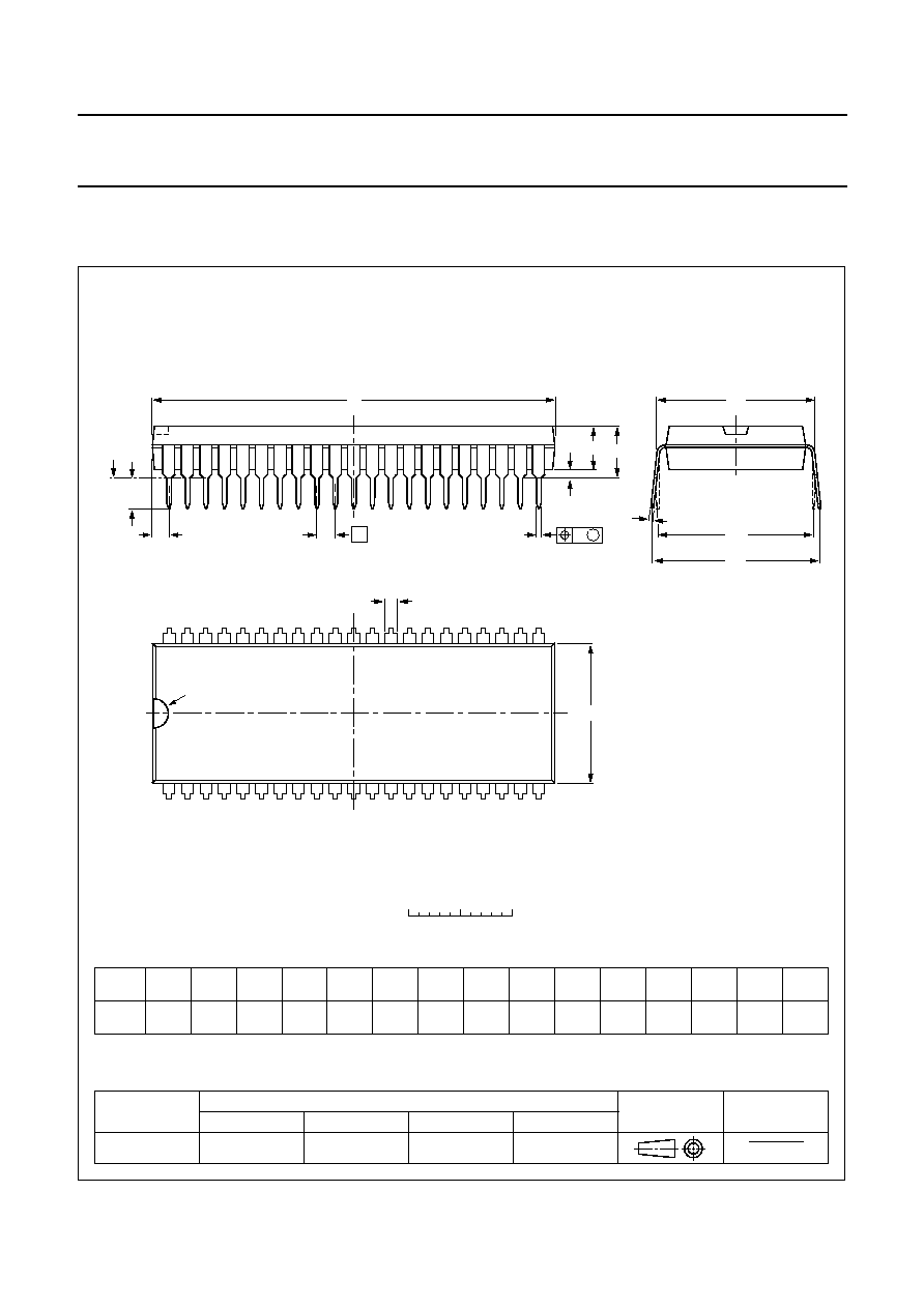
SDIP42: plastic shrink dual in-line package; 42 leads (600 mil)
SOT270-1

1997 Jul 03
31
Philips Semiconductors
Product specification
8-bit microcontrollers with LCD-driver
P83C434; P83C834
UNIT
A
1
A
2
A
3
b
p
c
E
(1)
e
H
E
L
L
p
Q
Z
y
w
v
REFERENCES
OUTLINE
VERSION
EUROPEAN
PROJECTION
ISSUE DATE
IEC
JEDEC
EIAJ
mm
0.25
0.05
1.85
1.65
0.25
0.40
0.20
0.25
0.14
10.1
9.9
0.8
1.3
12.9
12.3
0.85
0.75
1.2
0.8
10
0
o
o
0.15
0.1
0.15
DIMENSIONS (mm are the original dimensions)
Note
1. Plastic or metal protrusions of 0.25 mm maximum per side are not included.
0.95
0.55
SOT307-2
92-11-17
95-02-04
D
(1)
(1)
(1)
10.1
9.9
H
D
12.9
12.3
E
Z
1.2
0.8
D
e
E
B
11
c
E
H
D
ZD
A
Z E
e
v
M
A
X
1
44
34
33
23
22
12
y
A
1
A
L
p
Q
detail X
L
(A )
3
A
2
pin 1 index
D
H
v
M
B
b
p
b
p
w
M
w
M
0
2.5
5 mm
scale
QFP44: plastic quad flat package; 44 leads (lead length 1.3 mm); body 10 x 10 x 1.75 mm
SOT307-2
A
max.
2.10

1997 Jul 03
32
Philips Semiconductors
Product specification
8-bit microcontrollers with LCD-driver
P83C434; P83C834
14 SOLDERING
14.1
Introduction
There is no soldering method that is ideal for all IC
packages. Wave soldering is often preferred when
through-hole and surface mounted components are mixed
on one printed-circuit board. However, wave soldering is
not always suitable for surface mounted ICs, or for
printed-circuits with high population densities. In these
situations reflow soldering is often used.
This text gives a very brief insight to a complex technology.
A more in-depth account of soldering ICs can be found in
our
"IC Package Databook" (order code 9398 652 90011).
14.2
SDIP
14.2.1
S
OLDERING BY DIPPING OR BY WAVE
The maximum permissible temperature of the solder is
260
∞
C; solder at this temperature must not be in contact
with the joint for more than 5 seconds. The total contact
time of successive solder waves must not exceed
5 seconds.
The device may be mounted up to the seating plane, but
the temperature of the plastic body must not exceed the
specified maximum storage temperature (T
stg max
). If the
printed-circuit board has been pre-heated, forced cooling
may be necessary immediately after soldering to keep the
temperature within the permissible limit.
14.2.2
R
EPAIRING SOLDERED JOINTS
Apply a low voltage soldering iron (less than 24 V) to the
lead(s) of the package, below the seating plane or not
more than 2 mm above it. If the temperature of the
soldering iron bit is less than 300
∞
C it may remain in
contact for up to 10 seconds. If the bit temperature is
between 300 and 400
∞
C, contact may be up to 5 seconds.
14.3
QFP
14.3.1
R
EFLOW SOLDERING
Reflow soldering techniques are suitable for all QFP
packages.
The choice of heating method may be influenced by larger
plastic QFP packages (44 leads, or more). If infrared or
vapour phase heating is used and the large packages are
not absolutely dry (less than 0.1% moisture content by
weight), vaporization of the small amount of moisture in
them can cause cracking of the plastic body. For more
information, refer to the Drypack chapter in our
"Quality
Reference Handbook" (order code 9397 750 00192).
Reflow soldering requires solder paste (a suspension of
fine solder particles, flux and binding agent) to be applied
to the printed-circuit board by screen printing, stencilling or
pressure-syringe dispensing before package placement.
Several techniques exist for reflowing; for example,
thermal conduction by heated belt. Dwell times vary from
50 to 300 seconds depending on heating method. Typical
reflow temperatures range from 215 to 250
∞
C.
Preheating is necessary to dry the paste and evaporate
the binding agent. Preheat for 45 minutes at 45
∞
C.
14.3.2
W
AVE SOLDERING
Wave soldering is not recommended for QFP packages.
This is because of the likelihood of solder bridging due to
closely-spaced leads and the possibility of incomplete
solder penetration in multi-lead devices.
If wave soldering cannot be avoided, the following
conditions must be observed:
∑
A double-wave (a turbulent wave with high upward
pressure followed by a smooth laminar wave)
soldering technique should be used.
∑
The footprint must be at an angle of 45
∞
to the board
direction and must incorporate solder thieves
downstream and at the side corners.
Even with these conditions, do not consider wave
soldering the following packages: QFP52 (SOT379-1),
QFP100 (SOT317-1), QFP100 (SOT317-2),
QFP100 (SOT382-1) or QFP160 (SOT322-1).
During placement and before soldering, the package must
be fixed with a droplet of adhesive. The adhesive can be
applied by screen printing, pin transfer or syringe
dispensing. The package can be soldered after the
adhesive is cured. Maximum permissible solder
temperature is 260
∞
C, and maximum duration of package
immersion in solder is 10 seconds, if cooled to less than
150
∞
C within 6 seconds. Typical dwell time is 4 seconds
at 250
∞
C.
A mildly-activated flux will eliminate the need for removal
of corrosive residues in most applications.
14.3.3
R
EPAIRING SOLDERED JOINTS
Fix the component by first soldering two diagonally-
opposite end leads. Use only a low voltage soldering iron
(less than 24 V) applied to the flat part of the lead. Contact
time must be limited to 10 seconds at up to 300
∞
C. When
using a dedicated tool, all other leads can be soldered in
one operation within 2 to 5 seconds between
270 and 320
∞
C.

1997 Jul 03
33
Philips Semiconductors
Product specification
8-bit microcontrollers with LCD-driver
P83C434; P83C834
15 DEFINITIONS
16 LIFE SUPPORT APPLICATIONS
These products are not designed for use in life support appliances, devices, or systems where malfunction of these
products can reasonably be expected to result in personal injury. Philips customers using or selling these products for
use in such applications do so at their own risk and agree to fully indemnify Philips for any damages resulting from such
improper use or sale.
Data sheet status
Objective specification
This data sheet contains target or goal specifications for product development.
Preliminary specification
This data sheet contains preliminary data; supplementary data may be published later.
Product specification
This data sheet contains final product specifications.
Limiting values
Limiting values given are in accordance with the Absolute Maximum Rating System (IEC 134). Stress above one or
more of the limiting values may cause permanent damage to the device. These are stress ratings only and operation
of the device at these or at any other conditions above those given in the Characteristics sections of the specification
is not implied. Exposure to limiting values for extended periods may affect device reliability.
Application information
Where application information is given, it is advisory and does not form part of the specification.

1997 Jul 03
34
Philips Semiconductors
Product specification
8-bit microcontrollers with LCD-driver
P83C434; P83C834
NOTES

1997 Jul 03
35
Philips Semiconductors
Product specification
8-bit microcontrollers with LCD-driver
P83C434; P83C834
NOTES

Internet: http://www.semiconductors.philips.com
Philips Semiconductors ≠ a worldwide company
© Philips Electronics N.V. 1997
SCA54
All rights are reserved. Reproduction in whole or in part is prohibited without the prior written consent of the copyright owner.
The information presented in this document does not form part of any quotation or contract, is believed to be accurate and reliable and may be changed
without notice. No liability will be accepted by the publisher for any consequence of its use. Publication thereof does not convey nor imply any license
under patent- or other industrial or intellectual property rights.
Netherlands: Postbus 90050, 5600 PB EINDHOVEN, Bldg. VB,
Tel. +31 40 27 82785, Fax. +31 40 27 88399
New Zealand: 2 Wagener Place, C.P.O. Box 1041, AUCKLAND,
Tel. +64 9 849 4160, Fax. +64 9 849 7811
Norway: Box 1, Manglerud 0612, OSLO,
Tel. +47 22 74 8000, Fax. +47 22 74 8341
Philippines: Philips Semiconductors Philippines Inc.,
106 Valero St. Salcedo Village, P.O. Box 2108 MCC, MAKATI,
Metro MANILA, Tel. +63 2 816 6380, Fax. +63 2 817 3474
Poland: Ul. Lukiska 10, PL 04-123 WARSZAWA,
Tel. +48 22 612 2831, Fax. +48 22 612 2327
Portugal: see Spain
Romania: see Italy
Russia: Philips Russia, Ul. Usatcheva 35A, 119048 MOSCOW,
Tel. +7 095 755 6918, Fax. +7 095 755 6919
Singapore: Lorong 1, Toa Payoh, SINGAPORE 1231,
Tel. +65 350 2538, Fax. +65 251 6500
Slovakia: see Austria
Slovenia: see Italy
South Africa: S.A. PHILIPS Pty Ltd., 195-215 Main Road Martindale,
2092 JOHANNESBURG, P.O. Box 7430 Johannesburg 2000,
Tel. +27 11 470 5911, Fax. +27 11 470 5494
South America: Rua do Rocio 220, 5th floor, Suite 51,
04552-903 S„o Paulo, S√O PAULO - SP, Brazil,
Tel. +55 11 821 2333, Fax. +55 11 829 1849
Spain: Balmes 22, 08007 BARCELONA,
Tel. +34 3 301 6312, Fax. +34 3 301 4107
Sweden: Kottbygatan 7, Akalla, S-16485 STOCKHOLM,
Tel. +46 8 632 2000, Fax. +46 8 632 2745
Switzerland: Allmendstrasse 140, CH-8027 ZÐRICH,
Tel. +41 1 488 2686, Fax. +41 1 481 7730
Taiwan: Philips Semiconductors, 6F, No. 96, Chien Kuo N. Rd., Sec. 1,
TAIPEI, Taiwan Tel. +886 2 2134 2865, Fax. +886 2 2134 2874
Thailand: PHILIPS ELECTRONICS (THAILAND) Ltd.,
209/2 Sanpavuth-Bangna Road Prakanong, BANGKOK 10260,
Tel. +66 2 745 4090, Fax. +66 2 398 0793
Turkey: Talatpasa Cad. No. 5, 80640 GÐLTEPE/ISTANBUL,
Tel. +90 212 279 2770, Fax. +90 212 282 6707
Ukraine: PHILIPS UKRAINE, 4 Patrice Lumumba str., Building B, Floor 7,
252042 KIEV, Tel. +380 44 264 2776, Fax. +380 44 268 0461
United Kingdom: Philips Semiconductors Ltd., 276 Bath Road, Hayes,
MIDDLESEX UB3 5BX, Tel. +44 181 730 5000, Fax. +44 181 754 8421
United States: 811 East Arques Avenue, SUNNYVALE, CA 94088-3409,
Tel. +1 800 234 7381
Uruguay: see South America
Vietnam: see Singapore
Yugoslavia: PHILIPS, Trg N. Pasica 5/v, 11000 BEOGRAD,
Tel. +381 11 625 344, Fax.+381 11 635 777
For all other countries apply to: Philips Semiconductors, Marketing & Sales Communications,
Building BE-p, P.O. Box 218, 5600 MD EINDHOVEN, The Netherlands, Fax. +31 40 27 24825
Argentina: see South America
Australia: 34 Waterloo Road, NORTH RYDE, NSW 2113,
Tel. +61 2 9805 4455, Fax. +61 2 9805 4466
Austria: Computerstr. 6, A-1101 WIEN, P.O. Box 213,
Tel. +43 1 60 101, Fax. +43 1 60 101 1210
Belarus: Hotel Minsk Business Center, Bld. 3, r. 1211, Volodarski Str. 6,
220050 MINSK, Tel. +375 172 200 733, Fax. +375 172 200 773
Belgium: see The Netherlands
Brazil: see South America
Bulgaria: Philips Bulgaria Ltd., Energoproject, 15th floor,
51 James Bourchier Blvd., 1407 SOFIA,
Tel. +359 2 689 211, Fax. +359 2 689 102
Canada: PHILIPS SEMICONDUCTORS/COMPONENTS,
Tel. +1 800 234 7381
China/Hong Kong: 501 Hong Kong Industrial Technology Centre,
72 Tat Chee Avenue, Kowloon Tong, HONG KONG,
Tel. +852 2319 7888, Fax. +852 2319 7700
Colombia: see South America
Czech Republic: see Austria
Denmark: Prags Boulevard 80, PB 1919, DK-2300 COPENHAGEN S,
Tel. +45 32 88 2636, Fax. +45 31 57 0044
Finland: Sinikalliontie 3, FIN-02630 ESPOO,
Tel. +358 9 615800, Fax. +358 9 61580920
France: 4 Rue du Port-aux-Vins, BP317, 92156 SURESNES Cedex,
Tel. +33 1 40 99 6161, Fax. +33 1 40 99 6427
Germany: Hammerbrookstraþe 69, D-20097 HAMBURG,
Tel. +49 40 23 53 60, Fax. +49 40 23 536 300
Greece: No. 15, 25th March Street, GR 17778 TAVROS/ATHENS,
Tel. +30 1 4894 339/239, Fax. +30 1 4814 240
Hungary: see Austria
India: Philips INDIA Ltd, Shivsagar Estate, A Block, Dr. Annie Besant Rd.
Worli, MUMBAI 400 018, Tel. +91 22 4938 541, Fax. +91 22 4938 722
Indonesia: see Singapore
Ireland: Newstead, Clonskeagh, DUBLIN 14,
Tel. +353 1 7640 000, Fax. +353 1 7640 200
Israel: RAPAC Electronics, 7 Kehilat Saloniki St, PO Box 18053,
TEL AVIV 61180, Tel. +972 3 645 0444, Fax. +972 3 649 1007
Italy: PHILIPS SEMICONDUCTORS, Piazza IV Novembre 3,
20124 MILANO, Tel. +39 2 6752 2531, Fax. +39 2 6752 2557
Japan: Philips Bldg 13-37, Kohnan 2-chome, Minato-ku, TOKYO 108,
Tel. +81 3 3740 5130, Fax. +81 3 3740 5077
Korea: Philips House, 260-199 Itaewon-dong, Yongsan-ku, SEOUL,
Tel. +82 2 709 1412, Fax. +82 2 709 1415
Malaysia: No. 76 Jalan Universiti, 46200 PETALING JAYA, SELANGOR,
Tel. +60 3 750 5214, Fax. +60 3 757 4880
Mexico: 5900 Gateway East, Suite 200, EL PASO, TEXAS 79905,
Tel. +9-5 800 234 7381
Middle East: see Italy
Printed in The Netherlands
457047/00/03/pp36
Date of release: 1997 Jul 03
Document order number:
9397 750 02549