
DATA SHEET
Objective Specification
File under Integrated Circuits, IC20
1999 Aug 19
INTEGRATED CIRCUITS
P8xC591
Single-chip 8-bit microcontroller
with CAN controller

1999 Aug 19
2
Philips Semiconductors
Objective Specification
Single-chip 8-bit microcontroller with CAN controller
P8xC591
CONTENTS
1
FEATURES
1.1
80C51 Related Features of the 8xC591
1.2
CAN Related Features of the 8xC591
2
GENERAL DESCRIPTION
3
ORDERING INFORMATION
4
BLOCK DIAGRAM
5
FUNCTIONAL DIAGRAM
6
PINNING INFORMATION
6.1
Pinning diagram
6.2
Pin description
7
MEMORY ORGANIZATION
7.1
Program Memory
7.2
Addressing
7.3
Expanded Data RAM addressing
7.4
Dual DPTR
8
I/O FACILITIES
9
OSCILLATOR CHARACTERISTICS
10
RESET
11
LOW POWER MODES
11.1
Stop Clock Mode
11.2
Idle Mode
11.3
Power-down Mode
12
CAN, CONTROLLER AREA NETWORK
12.1
Features of the PeliCAN Controller
12.2
PeliCAN structure
12.3
Communication between PeliCAN Controller
and CPU
12.4
Register and Message Buffer description
12.5
CAN Registers
13
SERIAL I/O
14
SIO0 STANDARD SERIAL INTERFACE UART
14.1
Multiprocessor Communications
14.2
Serial Port Control Register
14.3
Baud Rate Generation
14.4
More about UART Modes
14.5
Enhanced UART
15
SIO1, I
2
C SERIAL IO
15.1
Modes of Operation
15.2
SIO1 Implementation and Operation
15.3
Software Examples of SIO1 Service Routines
16
TIMER 2
16.1
Features of Timer 2
17
WATCHDOG TIMER (T3)
18
PULSE WIDTH MODULATED OUTPUTS
18.1
Prescaler Frequency Control Register (PWMP)
18.2
Pulse Width Register 0 (PWM0)
18.3
Pulse Width Register 1 (PWM1)
19
PORT 1 OPERATION
20
ANALOG-TO-DIGITAL CONVERTER (ADC)
20.1
ADC features
20.2
ADC functional description
20.3
10-Bit Analog-to-Digital Conversion
20.4
10-Bit ADC Resolution and Analog Supply
20.5
Power Reduction Modes
21
INTERRUPTS
21.1
Interrupt Enable Registers
21.2
Interrupt Enable and Priority Registers
21.3
Interrupt priority
21.4
Interrupt Vectors
22
INSTRUCTION SET
22.1
Addressing Modes
23
LIMITING VALUES
24
DC CHARACTERISTICS (VALUES IN THIS
TABLE NOT CONFIRMED)
25
AC CHARACTERISTICS
25.1
Timing symbol definitions
26
EPROM CHARACTERISTICS
26.1
Program verification
26.2
Security bits
27
PACKAGE OUTLINES
28
SOLDERING
28.1
Plastic leaded-chip carriers/quad flat-packs
29
DEFINITIONS
30
LIFE SUPPORT APPLICATIONS

1999 Aug 19
3
Philips Semiconductors
Objective Specification
Single-chip 8-bit microcontroller with CAN controller
P8xC591
1
FEATURES
1.1
80C51 Related Features of the 8xC591
∑
Full static 80C51 Central Processing Unit available as
OTP, ROM and ROMless
∑
16 Kbytes internal Program Memory expandable
externally to 64 Kbytes
∑
512 bytes on-chip Data RAM expandable externally to
64 Kbytes
∑
Three 16-bit timers/counters T0, T1 (standard 80C51)
and additional T2 (capture & compare)
∑
10-bit ADC with 6 multiplexed analog inputs with fast
8-bit ADC option
∑
Two 8-bit resolution, Pulse Width Modulated outputs
∑
32 I/O port pins in the standard 80C51 pinout
∑
I
2
C-bus serial I/O port with byte oriented master and
slave functions
∑
On-chip Watchdog Timer T3
∑
Extended temperature range:
-
40 to +85
∞
C
∑
Accelerated (prescaler 1:1) instruction cycle time
375 ns @ 16 MHz
∑
Operation voltage range: 5 V
±
10%
∑
Security bits:
≠ ROM version has 2 bits
≠ OTP/EPROM version has 3 bits
∑
64 bytes Encryption array
∑
4 level priority interrupt, 15 interrupt sources
∑
Full-duplex enhanced UART with programmable
Baudrate Generator
∑
Power Control Modes:
≠ Clock can be stopped and resumed
≠ Idle Mode
≠ Power-down Mode
∑
ADC active in Idle Mode
∑
Second DPTR register
∑
ALE inhibit for EMI reduction
∑
Programmable I/O port pins (pseudo bi-directional,
push-pull, high impedance, open drain)
∑
Wake-up from Power-down by external interrupts
∑
Software reset bit (AUXR1.5)
∑
Low active reset pin
∑
Power-on detect reset
∑
Once mode
1.2
CAN Related Features of the 8xC591
∑
CAN 2.0B active controller, supporting 11-bit Standard
and 29-bit Extended indentifiers
∑
1 Mbit/s CAN bus speed with 8 MHz clock achievable
∑
64 byte receive FIFO (can capture sequential Data
Frames from the
same source as required by the
Transport Layer of higher protocols such as DeviceNet,
CANopen and OSEK)
∑
13 byte transmit buffer
∑
Enhanced PeliCAN core (from the SJA1000 stand-alone
CAN2.0B controller)
1.2.1
P
ELI
CAN F
EATURES
∑
Four independently configurable Screeners
(Acceptance Filters)
∑
Each Screener has tow 32-bit specifiers:
≠ 32-bit Match and
≠ 32-bit Mask
∑
32-bits of Mask
per Screener allows unique Group
addressing per
Screener
∑
Higher layer protocols especially supported in Standard
CAN format with:
≠ Up to four, 11-bit ID Screeners that also Screen the
two (2) Data Bytes
≠ i.e., Data Frames are Screened by the CAN ID and by
Data Byte content
∑
Up to eight, 11-bit ID Screeners half of which
also
Screen the
first Data Byte
∑
All Screeners are changeable "on the fly"
∑
Listen Only Mode, Self Test Mode
∑
Error Code Capture, Arbitration Lost Capture, readable
Error Counters

1999 Aug 19
4
Philips Semiconductors
Objective Specification
Single-chip 8-bit microcontroller with CAN controller
P8xC591
2
GENERAL DESCRIPTION
The P8xC591 is a single-chip 8-bit-high-performance
microcontroller, with on-chip CAN-controller, derived from
the 80C51 microcontroller family.
It uses the powerful 80C51 instruction set and includes the
successful PeliCAN functionality of the SJA1000 CAN
controller from Philips Semiconductors.
The fully static core provides extended power save
provisions as the oscillator can be stopped and easily
restarted without loss of data. The improved internal clock
prescaler of 1:1 achieves a 375 ns instruction cycle time at
16 MHz external clock rate.
Figure 1 shows a Block Diagram of the P8xC591. The
microcontroller is manufactured in an advanced CMOS
process, and is designed for use in automotive and
general industrial applications. In addition to the 80C51
standard features, the device provides a number of
dedicated hardware functions for these applications.
Three versions of the P8xC591 will be offered:
∑
P80C591 (without ROM)
∑
P83C591 (with ROM)
∑
P87C591 (with OTP)
Hereafter these versions will be referred to as P8xC591.
The temperature range includes (max. f
CLK
= 16 MHz):
∑
-40 to +85
∞
C version, for general applications
The P8xC591 combines the functions of the P87C554
(microcontroller) and the SJA1000 (stand-alone
CAN-controller) with the following enhanced features:
∑
Enhanced CAN receive interrupt (level sensitive)
∑
Extended acceptance filter
∑
Acceptance filter changeable "on the fly".
The main differences between P8xC591 and P87C554
are:
∑
CAN-controller on chip
∑
6-input ADC
∑
Low active Reset
∑
44 leads.
3
ORDERING INFORMATION
TYPE NUMBER
PACKAGE
TEMPERATURE
RANGE (
∞
C)
NAME
DESCRIPTION
VERSION
P80C591SFA
PLCC44
plastic leaded chip carrier; 44 leads
SOT187-2
-
40 to +85
P83C591SFA
P87C591SFA
P80C591SFB
QFP44
plastic quad flat package; 44 leads (lead length 1.3 mm);
body 10
◊
10
◊
1.75 mm
SOT307-2
P83C591SFB
P87C591SFB

1999 Aug 19
5
Philips Semiconductors
Objective Specification
Single-chip 8-bit microcontroller with CAN controller
P8xC591
4
BLOCK DIAGRAM
Fig.1 Block diagram P8xC591.
handbook, full pagewidth
MHI001
16-BIT TIMER/EVENT
COUNTER WITH CAPTURE
(T2)
PARALLEL
I/O PORTS
WATCHDOG
TIMER (T3)
TWO 16-BIT
TIMER/EVENT
COUNTERS
(T0/T1)
16 KBYTES
PROGRAM
MEMORY
512 BYTES
DATA
MEMORY
CPU
CORE
OSCILLATOR
I
2
C SERIAL
INTERFACE
CPU
INTERFACE
(SFRs)
TXDC
SCL
SDA
RT2
T2
P3
P2
P1
P0
RST
A0 to A7
VDD
VSS
XTAL2
XTAL1
CMSR0 to 5
CMT0 to 1
CT0x/INTx
RXDC
UART
RXD
TXD
CAN 2.0 B
INTERFACE
PWM
PWM0
AN0 to 5
AVref
+
AVSS
EA
PWM1
ADC
P8xC591
T1
T0
80C51 CONFIGURABLE CORE
INT1
INT0
RD
WR
PSEN
ALE

1999 Aug 19
6
Philips Semiconductors
Objective Specification
Single-chip 8-bit microcontroller with CAN controller
P8xC591
5
FUNCTIONAL DIAGRAM
Fig.2 Functional diagram.
handbook, full pagewidth
MHI002
P8xC591
(44-PIN)
0
1
2
3
4
5
6
7
PORT 0
VDD
VSS
0
1
2
3
4
5
6
7
PORT 1
0
1
2
3
4
5
6
7
PORT 2
address bus
AD0
AD1
AD2
AD3
AD4
AD5
AD6
AD7
and data bus
low order address
alternative functions
RXDC
CAN
I
2
C
TXDC
ADC0
ADC1
ADC2
ADC3
CT0I/INT2
CT1I/INT3
CT2I/INT4
CT3I/INT5
ADC4
ADC5
SCL
SDA
0
1
2
3
4
5
6
7
PORT 3
RXD
TXD
INT0
INT1
T0
T1
T2
RT2
CSMR0
CSMR1
CSMR2
CSMR3
WR
RD
AVref
+
AVSS
PWM1
PWM0
EA
ALE
XTAL1
XTAL2
PSEN
RST

1999 Aug 19
7
Philips Semiconductors
Objective Specification
Single-chip 8-bit microcontroller with CAN controller
P8xC591
6
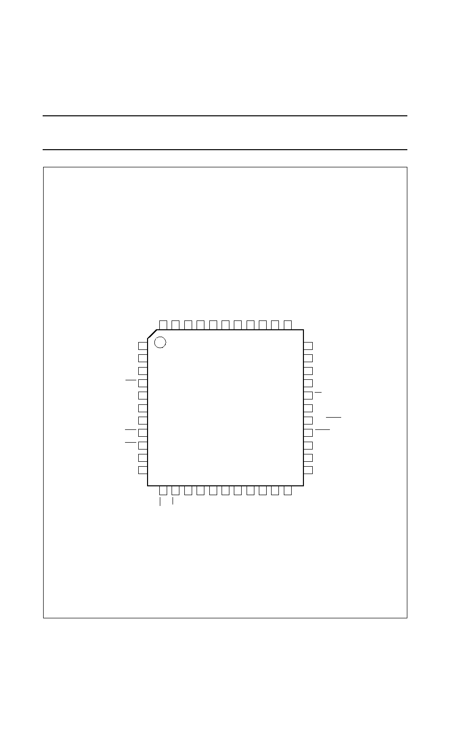
PINNING INFORMATION
6.1
Pinning diagram
Fig.3 Pinning Diagram for 44-lead LCC Package.
handbook, full pagewidth
P8xC591
MHI003
7
8
9
10
11
12
13
14
15
16
17
39
38
37
36
35
34
33
32
31
30
29
18
19
20
21
22
23
24
25
26
27
28
6
5
4
3
2
1
44
43
42
41
40
P1.4/ADC2/INT4/CT2I
P1.3/ADC1/INT3/CT1I
P1.2/ADC0/INT2/CT0I
P1.1/TXDC
P1.0/RXDC
AV
SS
AV
ref
+
P0.0/AD0
P0.1/AD1
P0.2/AD2
P0.3/AD3
P3.6/WR
P3.7/RD
XTAL2
XTAL1
V
SS
V
DD
P2.0/A8
P2.1/A9
P2.2/A10
P2.3/A11
P2.4/A12
CT3I/INT5/ADC3/P1.5
SCL/ADC4/P1.6
SDA/ADC5/P1.7
RST
T2/P3.0/RXD
PWM0
RT2/P3.1/TXD
CMSR0/P3.2/INT0
CMSR1/P3.3/INT1
CMSR2/P3.4/T0
CMSR3/P3.5/T1
P0.4/AD4
P0.5/AD5
P0.6/AD6
P0.7/AD7
EA/VPP
PWM1
ALE/PROG
PSEN
P2.7/A15
P2.6/A14
P2.5/A13
1999 Aug 19
8
Philips Semiconductors
Objective Specification
Single-chip 8-bit microcontroller with CAN controller
P8xC591
Fig.4 Pinning Diagram for 44-lead Plastic Quad Flat Package (QFP).
handbook, full pagewidth
P8xC591
MHI004
1
2
3
4
5
6
7
8
9
10
11
33
32
31
30
29
28
27
26
25
24
23
12
13
14
15
16
17
18
19
20
21
22
44
43
42
41
40
39
38
37
36
35
34
P1.4/ADC2/INT4/CT2I
P1.3/ADC1/INT3/CT1I
P1.2/ADC0/INT2/CT0I
P1.1/TXDC
P1.0/RXDC
AV
SS
AV
ref
+
P0.0/AD0
P0.1/AD1
P0.2/AD2
P0.3/AD3
P3.6/WR
P3.7/RD
XTAL2
XTAL1
V
SS
V
DD
P2.0/A8
P2.1/A9
P2.2/A10
P2.3/A11
P2.4/A12
P1.5/ADC3/INT5/CT3I
P1.6/ADC4/SCL
P1.7/ADC5/SDA
RST
P3.0/T2/RXD
PWM0
RT2/P3.1/TXD
CMSR0/P3.2/INT0
CMSR2/P3.4/T0
CMSR3/P3.5/T1
P0.4/AD4
P0.5/AD5
P0.6/AD6
P0.7/AD7
EA/VPP
PWM1
ALE/PROG
PSEN
P2.7/A15
P2.6/A14
P2.5/A13
CMSR1/P3.3/INT1

1999 Aug 19
9
Philips Semiconductors
Objective Specification
Single-chip 8-bit microcontroller with CAN controller
P8xC591
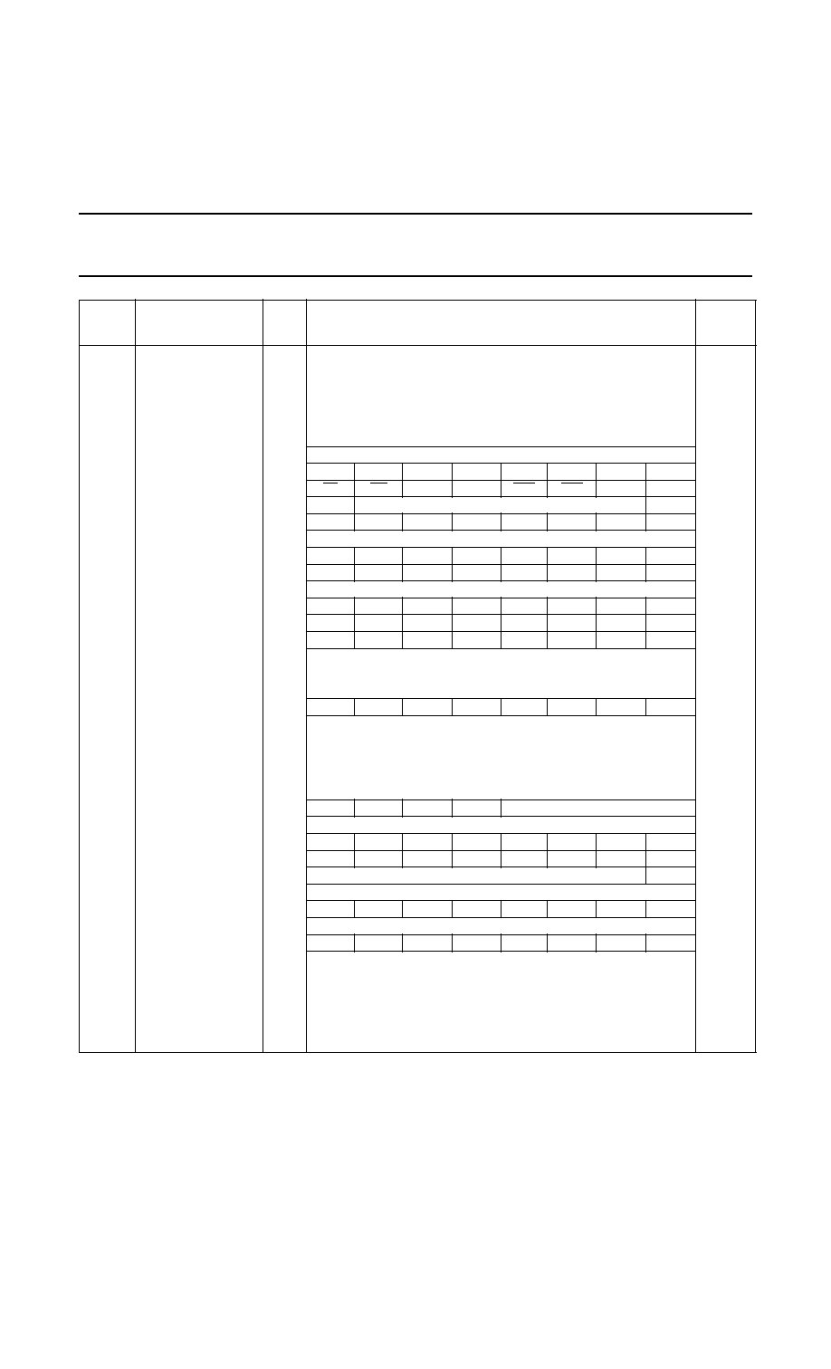
6.2
Pin description
Table 1
Pin description for QFP44/PLCC44, see Note 1.
SYMBOL
PIN
DESCRIPTION
QFP44
PLCC44
RST
4
10
Reset: A Input to reset the P8xC591. It also provides a reset pulse as output
when Timer T3 overflows.
P3.0to P3.7
Port 3 (P3.0 to P3.7): 8-bit programmable I/O port lines; Port 3 can
sink/source 4 LSTTL inputs.
Port 3 pins serve alternate functions as follows:
P3.0/RXD
5
11
RXD: Serial input port for UART;
T2: T2 event input
P3.1/TXD
7
13
TXD: Serial output port for UART;
RT2: T2 timer reset signal. Rising edge triggered.
P3.2/INT0/CMSR0 8
14
INT0: External interrupt input 0;
CMSR0: Compare and Set/Reset output for Timer T2.
P3.3/INT1/
CMSR1
9
15
INT1: External interrupt input 1;
CMSR1: Compare and Set/Reset output for Timer T2.
P3.4/T0/CMSR2
10
16
T0: Timer 0 external interrupt input;
CMSR2: Compare and Set/Reset output for Timer T2.
P3.5/T1/CMSR3
11
17
T1: Timer 1 external interrupt input;
CMSR3: Compare and Set/Reset output for Timer T2.
P3.6/WR
12
18
WR: External Data Memory Write strobe;
P3.7/RD
13
19
RD: External Data Memory Read strobe.
During reset, Port 3 will be asynchronously driven resistive HIGH.
Port 3 has four modes selected on a per bit basis by writing to the P3M1 and
P3M2 registers as follows:
P3M1.x
0
0
1
1
P3M2.x
0
1
0
1
Mode Description
Pseudo-bidirectional (standard c51 configuration default)
Push-Pull
High impedance
Open drain
XTAL2
14
20
Crystal pin 2: output of the inverting amplifier that forms the oscillator. Left
open-circuit when an external oscillator clock is used.
XTAL1
15
21
Crystal pin 1: input to the inverting amplifier that forms the oscillator, and
input to the internal clock generator. Receives the external oscillator clock
signal when an external oscillator is used.
V
SS
16
22
Ground; circuit ground potential.
V
DD
17
23
Power supply; power supply pin during normal operation and power
reduction modes.

1999 Aug 19
10
Philips Semiconductors
Objective Specification
Single-chip 8-bit microcontroller with CAN controller
P8xC591
P2.0/A08 to
P2.7/A15
18 to 25 24 to 31
Port 2 (P2.0 to P2.7): 8-bit programmable I/O port lines;
A08 to A15: High-order address byte for external memory.
Alternate function: High-order address byte for external memory (A08-A15).
Port 2 is also used to input the upper order address during EPROM
programming and verification. A8 is on P2.0, A9 on P2.1, through A12 on
P2.4.
During reset, Port 2 will be asynchronously driven HIGH.
Port 2 has four output modes selected on a per bit basis by writing to the
P2M1 and P2M2 registers as follows:
P2M1.x
0
0
1
1
P2M2.x
0
1
0
1
Mode Description
Pseudo-bidirectional (standard c51 configuration default)
Push-Pull
High impedance
Open drain
PSEN
26
32
Program Store Enable output: read strobe to the external Program Memory
via Ports 0 and 2. Is activated twice each machine cycle during fetches from
external Program Memory. When executing out of external Program Memory
two activations of PSEN are skipped during each access to external Data
Memory. PSEN is not activated (remains HIGH) during no fetches from
external Program Memory. PSEN can sink/source 8 LSTTL inputs. It can
drive CMOS inputs without external pull-ups.
ALE/PROG
27
33
Address Latch Enable output. Latches the low byte of the address during
access of external memory in normal operation. It is activated every six
oscillator periods except during an external Data Memory access. ALE can
sink/source 8 LSTTL inputs. It can drive CMOS inputs without an external
pull-up. To prohibit the toggling of ALE pin (RFI noise reduction) the bit A0
(SFR: AUXR.0) must be set by software; see Table 4.
PROG: the programming pulse input; alternative function for the P87C591.
EA/V
PP
29
35
External Access input. If, during reset, EA is held at a TTL level HIGH the
CPU executes out of the internal Program Memory. If, during reset, EA is held
at a TTL level LOW the CPU executes out of external Program Memory via
Port 0 and Port 2. EA is not allowed to float. EA is latched during reset and
don't care after reset.
V
PP
: the programming supply voltage; alternative function for the P87C591.
P0.0/AD0 to
P0.7/AD7
30 to 37 36 to 43
Port 0: 8-bit open-drain bidirectional I/O port.
During reset, Port 0 is HIGH-Impedance (Tri-State).
AD7 to AD0: Multiplexed Low-order address and Data bus for external
memory. During these accesses internal pull-ups are activated. Port 0 can
sink/source up to 8 LSTTL inputs.
AV
ref+
38
44
Analog to Digital Conversion Reference Resistor: High-end.
AV
SS
39
1
Analog ground.
SYMBOL
PIN
DESCRIPTION
QFP44
PLCC44

1999 Aug 19
11
Philips Semiconductors
Objective Specification
Single-chip 8-bit microcontroller with CAN controller
P8xC591
Notes
1. To avoid "latch-up" effect as power-on, the voltage on any pin at any time must not be higher or lower than V
DD
+
0.5 V
or V
SS
-
0.5 V.
2. Not implemented for P1.6 and P1.7.
P1.0 to P1.4
P1.5 to P1.7
40 to 44
1 to 3
2 to 6
7 to 9
Port 1: 8-bit I/O port with a user configurable output type. The operation of
Port 1 pins as inputs or outputs depends upon the port configuration selected.
Each port pin is configured independently.
Port 1 also provides various special functions as described below:
P1.0
40
2
RXDC: CAN Receiver input line.
P1.1
41
3
TXDC: CAN Transmit output line.
During reset, Port P1.0 and P1.1 will be asynchronously driven resistive
HIGH, P1.2 to P1.7 is High-Impedance (Tri-state).
P1.2 to P1.4
42 to 44 4 to 6
CT0I/INT2 / CT1I/INT3 / CT2I/INT4: T2 Capture timer inputs or External
Interrupt inputs.
P1.5 to P1.7
1 to 3
7 to 9
ADC0 to ADC2: Alternate function: Input channels to ADC.
ADC3 to ADC5: Input channels to ADC:
P1.5
1
7
CT3I/INT5: T2 Capture timer input or External Interrupt inputs.
P1.6
2
8
SCL: Serial port clock line I
2
C.
P1.7
3
9
SDA: Serial data clock line I
2
C.
Port 1 has four modes selected on a per bit basis by writing to the P1M1 and
P1M2 registers as follows:
P1M1.x
0
0
1
1
P1M2.x
0
1
0
1
Mode Description
Pseudo-bidirectional (standard c51 configuration default
(2)
)
Push-Pull
(2)
High impedance
Open drain
Port 1 is also used to input the lower order address byte during EPROM
programming and verification. A0 is on P1.0, etc.
PWM0
6
12
Pulse Width Modulation: Output 0.
PWM1
28
34
Pulse Width Modulation: Output 1.
SYMBOL
PIN
DESCRIPTION
QFP44
PLCC44

1999 Aug 19
12
Philips Semiconductors
Objective Specification
Single-chip 8-bit microcontroller with CAN controller
P8xC591
7
MEMORY ORGANIZATION
The Central Processing Unit (CPU) manipulates operands in three memory spaces as follows (see Fig.5):
∑
16 kbytes internal resp. 64 kbytes external Program Memory
∑
512 bytes internal Data Memory Main-and Auxiliary RAM
∑
up to 64 kbytes external Data Memory (with 256 bytes residing in the internal Auxiliary RAM).
Fig.5 Memory map and address space with EXTRAM = 0.
handbook, full pagewidth
MHI005
INDIRECT ONLY
DIRECT AND
INDIRECT
AUXILIARY
RAM
(EXTRAM = 0)
SFRs
255
127
0
EXTERNAL
(EA = 0)
INTERNAL
(EA = 1)
MAIN RAM
INTERNAL DATA MEMORY
EXTERNAL
DATA MEMORY
PROGRAM MEMORY
EXTERNAL
64K
64K
16384
16383
0
OVERLAPPED SPACE
256

1999 Aug 19
13
Philips Semiconductors
Objective Specification
Single-chip 8-bit microcontroller with CAN controller
P8xC591
7.1
Program Memory
The P8xC591 contains 16 Kbytes of on-chip Program
Memory which can be extended to 64 Kbytes with external
memories. When EA pin is held HIGH, the P8xC591
fetches instructions from internal ROM unless the address
exceeds 3FFFh. Locations 4000h to FFFFh are fetched
from external Program Memory. When the EA pin is held
LOW, all instruction fetches are from external memory.
The EA pin is latched during reset and is "don't care" after
reset.
Both, for the ROM and EPROM version of the P8xC591,
precautions are implemented to protect the device against
illegal Program Memory code reading.
7.2
Addressing
The P8xC591 has five methods for addressing the
Program and Data memory:
∑
Register
∑
Direct
∑
Register-Indirect
∑
Immediate
∑
Base-Register plus Index-Register-Indirect.
For more details about Addressing modes please refer to
Section 22.1 "Addressing Modes".
7.3
Expanded Data RAM addressing
The P8xC591 has internal data memory that is mapped
into four separate segments: the lower 128 bytes of RAM,
upper 128 bytes of RAM, 128 bytes Special Function
Register (SFR), and 256 bytes Auxiliary RAM (AUX-RAM)
as shown in Figure 5.
The four segments are:
1. The Lower 128 bytes of RAM (addresses 00H to 7FH)
are directly and indirectly addressable (see Fig.6).
2. The Upper 128 bytes of RAM (addresses 80H to FFH)
are indirectly addressable.
3. The Special Function Registers, SFRs, (addresses
80H to FFH) are directly addressable only. All these
SFRs are described in Table 4.
4. The 256-bytes AUX-RAM (00H - FFH) are indirectly
accessed by move external instruction, MOVX, and
within the EXTRAM bit cleared, see Table 3.
The Lower 128 bytes can be accessed by either direct or
indirect addressing. The Upper 128 bytes can be
accessed by indirect addressing only. The Upper 128
bytes occupy the same address space as the SFR. That
means they have the same address, but are physically
separate from SFR space.
When an instruction accesses an internal location above
address 7FH, the CPU knows whether the access is to the
upper 128 bytes of data RAM or to SFR space by the
addressing mode used in the instruction. Instructions that
use direct addressing access SFR space.
For example:
MOV 0A0H,#data
accesses the SFR at location 0A0H (which is P2).
Instructions that use indirect addressing access the Upper
128 bytes of data RAM.
For example:
MOV @ R0,#data
where R0 contains 0A0H, accesses the data byte at
address 0A0H, rather than P2 (whose address is 0A0H).
The AUX-RAM can be accessed by indirect addressing,
with EXTRAM bit cleared and MOVX instructions. This
part of memory is physically located on-chip, logically
occupies the first 256-bytes of external data memory.
With EXTRAM = 0, the AUX-RAM is indirectly addressed,
using the MOVX instruction in combination with any of the
registers R0, R1 of the selected bank or DPTR. An access
to AUX-RAM will not affect ports P0, P3.6 (WR#) and P3.7
(RD#). P2 SFR is output during external addressing. For
example, with EXTRAM = 0,
MOV @ R0,#data
where R0 contains 0A0h, access the AUX-RAM at
address 0A0H rather than external memory. An access to
external data memory locations higher than FFH (i.e.,
0100H to FFFFH) will be performed with the MOVX DPTR
instructions in the same way as in the standard 80C51, so
with P0 and P2 as data/address bus, and P3.6 and P3.7
as write and read timing signals. Refer to Table 4.
With EXTRAM = 1, MOVX @ Ri and MOVX @ DPTR will
be similar to the standard 80C51. MOVX @ Ri will provide
an 8-bit address multiplexed with data on Port 0 and any
output port pins can be used to output higher order
address bits. This is to provide the external paging
capability. MOVX @ DPTR will generate a 16-bit address.
Port 2 outputs the high-order eight address bits (the
contents of DPH) while Port 0 multiplexes the low-order
eight address bits (DPL) with data. MOVX @ Ri and MOVX
@ DPTR will generate either read or write signals on P3.6
(#WR) and P3.7 (#RD).
The stack pointer (SP) may be located anywhere in the
256 bytes RAM (lower and upper RAM) internal data
memory. The stack cannot be located in the AUX-RAM.

1999 Aug 19
14
Philips Semiconductors
Objective Specification
Single-chip 8-bit microcontroller with CAN controller
P8xC591
Table 2
AUX-RAM Page Register (address 8EH)
Table 3
Description of AUX-RAM bits
Notes
1. User software should not write `1's to reserved bits. These bits may be used in future 80C51 family products to invoke
new features. In that case, the reset or inactive of the new bit will be 0, and its active value will be `1'. The value read
from a reserved bit is indeterminate.
2. Reset value is `xxxxxx10B'.
7
6
5
4
3
2
1
0
-
-
-
-
-
LVADC
EXTRAM
AO
BIT
SYMBOL
FUNCTION
7 to 3
-
Reserved for future use; see Note 1.
2
LVADC
Enable A/D low voltage operation.
LVADC
0
1
Operating Mode
Turns off A/D charge pump.
Turns on A/D charge pump. Required for operation below 4 V.
1
EXTRAM
Internal/External RAM (00H - FFH) access using MOVX @ RI / @ DPTR
EXTRAM
0
1
Operating Mode
Internal AUX-RAM (00H - FH) access using MOVX @ RI / @ DPTR.
External data memory access.
0
AO
Disable/Enable ALE.
AO
0
1
Operating Mode
ALE is permitted at a constant rate of 1/6 the oscillator frequency.
ALE is active only during a MOVX or MOVC instruction.

1999 Aug 19
15
Philips Semiconductors
Objective Specification
Single-chip 8-bit microcontroller with CAN controller
P8xC591
Fig.6 Internal Main RAM bit addresses.
handbook, full pagewidth
MHI006
7F
7E
7D
7C
7B
7A
79
78
77
76
75
74
73
72
71
70
6F
6E
6D
6C
6B
6A
69
68
67
66
65
64
63
62
61
60
5F
5E
5D
5C
5B
5A
59
58
57
56
55
54
53
52
51
50
4F
4E
4D
4C
4B
4A
49
48
47
46
45
44
43
42
41
40
3F
3E
3D
3C
3B
3A
39
38
37
36
35
34
33
32
31
30
2F
2E
2D
2C
2B
2A
29
28
27
26
25
24
23
22
21
20
1F
1E
1D
1C
1B
1A
19
18
17
16
15
14
13
12
11
10
0F
0E
0D
0C
0B
0A
09
08
07
06
05
04
03
02
01
00
18h
17h
10h
0Fh
08h
07h
00h
24
23
31
16
15
8
7
0
REGISTER BANK 3
REGISTER BANK 2
REGISTER BANK 1
REGISTER BANK 0
32
33
34
35
36
37
38
39
40
41
42
43
44
45
46
47
(MSB)
(LSB)
127
7Fh
2Fh
2Eh
2Dh
2Ch
2Bh
2Ah
29h
28h
27h
26h
25h
24h
23h
22h
21h
20h
1Fh

1999 Aug 19
16
Philips Semiconductors
Objective Specification
Single-chip 8-bit microcontroller with CAN controller
P8xC591
7.3.1
S
PECIAL
F
UNCTION
R
EGISTERS
Table 4
Special Function Register Bit Address, Symbol or Alternate Port Function
* = SFRs are bit addressable; # = SFRs are modified from or added to the 80C51 SFRs.
NAME
DESCRIPTION
SFR
ADDR
BIT FUNCTIONS AND ADDRESSES
RESET
VALUE
MSB
LSB
ACC*
Accumulator
E0H
E7
E6
E5
E4
E3
E2
E1
E0
00H
ADCH#
A/D converter high
C6H
xxxxxxxxb
ADCON#
A/D control
C5H
ADC.1
ADC.0
-
ADCI
ADCS
AADR2
AADR1
AADR0
xx000000b
AUXR
Auxiliary
8EH
-
-
-
-
-
LVADC
EXTRAM
A0
xxxxx110B
AUXR1
Auxiliary
A2H
ADC8
AIDL
SRST
WDE
WUPD
0
-
DPS
000000x0B
B*
B register
F0H
F7
F6
F5
F4
F3
F2
F1
F0
00H
CTCON#
Capture control
EBH
CTN3
CTP3
CTN2
CTP2
CTN1
CTP1
CTN0
CTP0
00H
CTH3#
Capture high 3
CFH
xxxxxxxxB
CTH2#
Capture high 2
CEH
xxxxxxxxB
CTH1#
Capture high 1
CDH
xxxxxxxxB
CTH0#
Capture high 0
CCH
xxxxxxxxB
CMH2#
Compare high 2
CBH
00H
CMH1#
Compare high 1
CAH
00H
CMH0#
Compare high 0
C9H
00H
CTL3#
Capture low 3
AFH
xxxxxxxxB
CTL2#
Capture low 2
AEH
xxxxxxxxB
CTL1#
Capture low 1
ADh
xxxxxxxxB
CTL0#
Capture low 0
ACH
xxxxxxxxB
CML2#
Compare low 2
ABH
00H
CML1#
Compare low 1
AAH
00H
CML0#
Compare low 0
A9H
00H
DPTR:
Data Pointer (2 bytes):
DPH
Data Pointer High
83h
00H
DPL
Data Pointer Low
82h
00H
AF
AE
AD
AC
AB
AA
A9
A8
IENO*#
Interrupt Enable 0
A8H
EA
EAD
ES1
ES0
ET1
EX1
ET0
EX0
00H
EF
EE
ED
EC
EB
EA
E9
E8
IEN1*#
Interrupt Enable 1
E8H
ET2
ECAN
ECM1
ECM0
ECT3
ECT2
ECT1
ECT0
00H
BF
BE
BD
BC
BB
BA
B9
B8
IP0*#
Interrupt Priority 0
B8H
-
PAD
PS1
PS0
PT1
PX1
PT0
PX0
x0000000B
FF
FE
FD
FC
FB
FA
F9
F8
IP0H
Interrupt Priority 0 high
B7H
-
PADH
PS1H
PS0H
PT1H
PX1H
PT0H
PX0H
x0000000B
IP1*#
Interrupt Priority 1
F8h
PT2
PCAN
PCM1
PCM0
PCT3
PCT2
PCT1
PCT0
00H
IP1H
Interrupt Priority 1 high
F7H
PT2H
PCANH
PCM1H
PCM0H
PCT3H
PCT2H
PCT1H
PCT0H
00H
CANMOD
CAN Mode Register
C4H
00H
CANCON
CAN Command (w) and
Interrupt (r)
C3H
00H
CANDAT
CAN Data
C2H
00H
CANADR
CAN Address
C1H
00H
C7
C6
C5
C4
C3
C2
C1
C0
CANSTA
CAN Status (r)
C0H
BS
ES
TS
RS
TCS
TBS
DOS
RBS
00H
CAN Interrupt Enable (w)
BEIE
ALIE
EPIE
WUIE
DOIE
EIE
TIE
RIE
1999 Aug 19
17
Philips Semiconductors
Objective Specification
Single-chip 8-bit microcontroller with CAN controller
P8xC591
P1M1
Port 1 output mode 1
92H
FCH
P1M2
Port 1 output mode 2
93H
00H
P2M1
Port 2 output mode 1
94H
00H
P2M2
Port 2 output mode 2
95H
00H
P3M1
Port 3 output mode 1
9AH
00H
P3M2
Port 3 output mode 2
9BH
00H
B7
B6
B5
B4
B3
B2
B1
B0
-
-
CSMR3
CSMR2
CSMR1
CSMR0
RT2
T2
P3*
Port 3
B0H
RD
WR
T1
T0
INT1
INT0
TXD
RXD
FFH
A7
A6
A5
A4
A3
A2
A1
A0
P2*
Port 2
A0H
A15
A14
A13
A12
A11
A10
A9
A8
FFH
97
96
95
94
93
92
91
90
ADC5
ADC4
ADC3
ADC2
ADC1
ADC0
-
-
P1*
Port 1
90H
SDA
SCL
CT3I
CT2I
CT1I
CT0I
TXDC
RXDC
FFH
87
86
85
84
83
82
81
80
P0*
Port 0
80H
AD7
AD6
AD5
AD4
AD3
AD2
AD1
AD0
FFH
PCON
Power Control
87H
SMOD1
SMOD0
POF
WLE
GF1
GF0
PD
IDL
00x00000B
PSW
Program Status Word
D0H
CY
AC
F0
RS1
RS0
OV
F1
P
00H
PWMP#
PWM Prescaler
FEH
00H
PWMP1#
PWM Register 1
FDH
00H
PWMP0#
PWM Register 0
FCH
00H
RTE#
Reset Enable
EFH
RP35
RP34
RP33
RP32
xxxx0000B
S0ADDR
Serial 0 Slave Address
CBh
00H
S0ADEN
Slave Address Mask
F9H
00H
SP
Stack Pointer
81H
07H
S0BUF
Serial 0 Data Buffer
99H
xxxxxxxxB
S0PSL
Prescaler Value UART
FAH
00H
S0PSH
Prescaler/Value UART
FBH
SPS
Prescaler higher nibble
0xxx0000B
9F
9E
9D
9C
9B
9A
99
98
S0CON*
Serial 0 Control
98H
SM0/FE
SM1
SM2
REN
TB8
RB8
TI
RI
00H
S1CON#*
Serial 1Control
D8H
CR2
ENS1
STA
ST0
SI
AA
CR1
CR0
00H
S1ADR#
Serial 1 Address
DBH
SLAVE ADDRESS
GC
00H
S1DAT#
Serial 1 Data
DAH
00H
S1STA#
Serial 1 Status
D9H
SC4
SC3
SC2
SC1
SC0
0
0
0
F8H
DF
DE
DD
DC
DB
DA
D9
D8
STE#
Set Enable
EEH
SP35
SP34
SP33
SP32
xxxx0000B
TH1
Timer High 1
8DH
00H
TH0
Timer High 0
8CH
00H
TL1
Timer Low 1
8BH
00H
TL0
Timer Low 0
8AH
00H
TMH2#
Timer High 2
EDH
00H
TML2#
Timer Low 2
ECH
00H
NAME
DESCRIPTION
SFR
ADDR
BIT FUNCTIONS AND ADDRESSES
RESET
VALUE
MSB
LSB

1999 Aug 19
18
Philips Semiconductors
Objective Specification
Single-chip 8-bit microcontroller with CAN controller
P8xC591
TMOD
Timer Mode
89H
GATE
C/T
M1
M0
GATE
C/T
M1
M0
00H
8F
8E
8D
8C
8B
8A
89
88
TCON*
Timer Control
88H
TF1
TR1
TF0
TR0
IE1
IT1
IE0
IT0
00H
TM2CON#
Timer 2 Control
EAH
T2IS1
T2IS0
T2ER
T2B0
T2P1
T2P0
T2MS1
T2MS0
00H
CF
CE
CD
CC
CB
CA
C9
C8
TM2IR#*
Timer 2/CAN Int Flag Reg
C8H
T2OV
CMI2/
CAN
CMI1
CMI0
CTI3
CTI2
CTI1
CTI0
00H
T3#
Timer 3
FFH
00H
NAME
DESCRIPTION
SFR
ADDR
BIT FUNCTIONS AND ADDRESSES
RESET
VALUE
MSB
LSB

1999 Aug 19
19
Philips Semiconductors
Objective Specification
Single-chip 8-bit microcontroller with CAN controller
P8xC591
Fig.7 Dual DPTR:
handbook, full pagewidth
DPH
(83H)
BT0
AUXR1
DPS
DPL
(82H)
EXTERNAL
DATA
MEMORY
DPTR0
MHI007
DPTR1
7.4
Dual DPTR
The dual DPTR structure (see Figure 7) is a way by which
the chip will specify the address of an external data
memory location. There are two 16-bit DPTR registers that
address the external memory, and a single bit called DPS
= AUXR1/bit0 that allows the program code to switch
between them.
The DPS bit status should be saved by software when
switching between DPTR0 and DPTR1.
Note that bit 2 is not writable and is always read as a zero.
This allows the DPS bit to be quickly toggled simply by
executing an INC AUXR1 instruction without affecting the
other bits.
DPTR Instructions
The instructions that refer to DPTR refer to the data pointer
that is currently selected using the AUXR1/bit 0 register.
The six instructions that use the DPTR are as follows:
INC DPTRIncrements the data pointer by 1
MCV DPTR, #data 16
Loads the DPTR with a 16-bit
constant
MOV A, @ A+DPTR
Move code byte relative to
DPTR to ACC
MOVX A, @ DPTR
Move external RAM (16-bit
address) to ACC
MOVX @ DPTR, A
Move ACC to external RAM
(16-bit address)
JMP @ A + DPTR
Jump indirect relative to
DPTR
The data pointer can be accessed on a byte-by-byte basis
by specifying the low or high byte in an instruction which
accesses the SFRs. See application note AN458 for more
details.

1999 Aug 19
20
Philips Semiconductors
Objective Specification
Single-chip 8-bit microcontroller with CAN controller
P8xC591
7.4.1
AUXR1 P
AGE
R
EGISTER
Table 5
AUXR1 Page Register (address A2H)
Table 6
Description of AUXR1 of bits
User software should not write 1s to reserved bits. Theses bits may be used in future 8051 family products to invoke
new features. In that case, the reset or inactive value of the new bit will be logic 0, and its active value will be logic 1.
The value read from a reserved bit is indeterminate. The reset value of AUXR1 is (000000xB).
7
6
5
4
3
2
1
0
ADC8
AIDL
SRST
WDE
WUPD
0
-
DSP
BIT
SYMBOL
DESCRIPTION
7
ADC8
ADC Mode Switch. Switches between 10-bit conversion and 8-bit conversion
ADC8
0
1
Operating Mode
10-bit conversion (50 machine cycles)
8-bit conversion (24 machine cycles)
6
AIDL
Enables the ADC during Idle mode.
5
SRST
Software Reset.
4
WDE
Watchdog Timer Enable Flag.
3
WUPD
Enable Wake-up from Power-down.
2
0
Reserved.
1
-
Reserved.
0
DSP
Data Pointer Switch. Switches between DPRT0 and DPTR1.
ADC8
0
1
Operating Mode
DPTR0
DPTR1

1999 Aug 19
21
Philips Semiconductors
Objective Specification
Single-chip 8-bit microcontroller with CAN controller
P8xC591
8
I/O FACILITIES
The P8xC591 consists of 32 I/O Port lines with partly
multiple functions. The I/O's are held HIGH during reset
(asynchronous, before oscillator is running).
Ports 0, 1, 2 and 3 perform the following alternative
functions:
Port 0 is the same as in the 80C51. After reset the Port
Special Function Register is set to 'FFh' as known
from other 80C51 derivatives. Port 0 also provides
the multiplexed low-order address and data bus
used for expanding the P8xC591 with standard
memories and peripherals.
Port 1 supports several alternative functionalities. For this
reason it has different I/O stages. Note, port P1.0
and P1.1 are Driven-High and P1.2 to P1.7 are
High-Impedance (Tri-state) after reset.
Port 2 is the same as in the 80C51. After reset the Port
Special Function Register is set to 'FFh' as known
from other 80C51 derivatives. Port 2 also provides
the high-order address bus when the P8xC591 is
expanded with external Program Memory and/or
external Data Memory.
Port 3 is the same as in the 80C51. During reset the Port
3 Special Function Register is set to 'FFh' as known
from other 80C51 derivatives.
9
OSCILLATOR CHARACTERISTICS
XTAL1 and XTAL2 are the input and output, respectively,
of an inverting amplifier. The pins can be configured for
use as an on-chip oscillator, as shown in the logic symbol.
To drive the device from an external clock source, XTAL1
should be driven while XTAL2 is left unconnected. There
are no requirements on the duty cycle of the external clock
signal. However, minimum and maximum high and low
times specified in the data sheet must be observed.
10 RESET
A reset is accomplished by holding the RST pin LOW for
at least two machine cycles (12 oscillator periods), while
the oscillator is running. To insure a good power-on reset,
the RST pin must be low long enough to allow the oscillator
time to start up (normally a few milliseconds) plus two
machine cycles.
The RST line can also be pulled LOW internally by a
pull-down transistor activated by the watchdog timer T3.
The length of the output pulse from T3 is 3 machine cycles.
A pulse of such short duration is necessary in order to
recover from a processor or system fault as fast as
possible.
Note that the short reset pulse from Timer T3 cannot
discharge the power-on reset capacitor (see Figure 8).
Consequently, when the watchdog timer is also used to set
external devices, this capacitor arrangement should not be
connected to the RST pin, and a different circuit should be
used to perform the power-on reset operation. A timer T3
overflow, if enabled, will force a reset condition to the
P8xC591 by an internal connection, whether the output
RST is pulled-up HIGH or not.
A reset may be performed in software by setting the
software reset bit, SRST (AUXR1.5).
This device also has a Power-on Detect Reset circuit as
V
CC
transitions from V
CC
past V
RST
.
Fig.8 On-Chip Reset Configuration.
handbook, halfpage
MHI008
SCHMITT
TRIGGER
RESET
CIRCUITRY
RST
overflow
timer T3
on-chip
resistor
V
DD
Fig.9 Power-on Reset.
handbook, halfpage
MHI009
RST
RRST
2.2
µ
F
P8xC591
V
DD

1999 Aug 19
22
Philips Semiconductors
Objective Specification
Single-chip 8-bit microcontroller with CAN controller
P8xC591
11 LOW POWER MODES
11.1
Stop Clock Mode
The static design enables the clock speed to be reduced
down to 0 MHz (stopped). When the oscillator is stopped,
the RAM and Special Function Registers retain their
values. This mode allows step-by-step utilization and
permits reduced system power consumption by lowering
the clock frequency down to any value. For lowest power
consumption the Power-down mode is suggested.
11.2
Idle Mode
In the Idle mode (see Table 7), the CPU puts itself to sleep
while all of the on-chip peripherals stay active. The
instruction to invoke the idle mode is the last instruction
executed in the normal operating mode before the Idle
mode is activated. The CPU contents, the on-chip RAM,
and all of the special function registers remain intact during
this mode. The Idle mode can be terminated either by any
enabled interrupt (at which time the process is picked up
at the interrupt service routine and continued), or by a
hardware reset which starts the processor in the same
manner as a Power-on reset.
11.3
Power-down Mode
To save even more power, a Power-down mode (see
Table 7) can be invoked by software. In this mode, the
oscillator is stopped and the instruction that invoked Power
Down is the last instruction executed. The on-chip RAM
and Special Function Registers retain their values down to
2.0 V and care must be taken to return V
CC
to the minimum
specified operating voltages before the Power-down Mode
is terminated.
A hardware reset or external interrupt can be used to exit
from Power-down. The Wake-up from Power-down bit,
WUPD (AUXR1.3) must be set in order for an interrupt to
cause a Wake-up from Power-down. Reset redefines all
the SFRs but does not change the on-chip RAM. A
Wake-up allows both the SFRs and the on-chip RAM to
retain their values.
To properly terminate Power-down the reset or external
interrupt should not be executed before V
CC
is restored to
its normal operating level and must be held active long
enough for the oscillator to restart and stabilize (normally
less than 10 ms).
Table 7
Status of external pins during Idle and Power-down modes
With an external interrupt, INT0 and INT1 must be enabled and configured as level-sensitive. Holding the pin low restarts
the oscillator but bringing the pin back high completes the exit. Once the interrupt is serviced, the next instruction to be
executed after RETI will be the one following the instruction that put the device into Power-down.
MODE
MEMORY
ALE
PSEN
PORT 0
PORT 1
PORT 2
PORT 3
PWM0/
PWM1
Idle
internal
1
1
port data
port data
port data
port data
high
external
1
1
float
port data
address
port data
high
Power-down
internal
0
0
port data
port data
port data
port data
high
external
0
0
float
port data
port data
port data
high

1999 Aug 19
23
Philips Semiconductors
Objective Specification
Single-chip 8-bit microcontroller with CAN controller
P8xC591
11.3.1
P
OWER
O
FF
F
LAG
The Power Off Flag (POF) is set by on-chip circuitry when
the V
CC
level on the P8xC591 rises from 0 to 5 V. The POF
bit can be set or cleared by software allowing a user to
determine if the reset is the result of a power-on or warm
after Power-down. The V
CC
level must remain above 3 V
for the POF to remain unaffected by the V
CC
level.
11.3.2
D
ESIGN
C
ONSIDERATION
∑
When the Idle mode is terminated by a hardware reset,
the device normally resumes program execution, from
where it left off, up to two machine cycles before the
internal reset algorithm takes control. On-chip hardware
inhibits access to internal RAM in this event, but access
to the port pins is not inhibited. To eliminate the
possibility of an unexpected write when Idle is
terminated by reset, the instruction following the one
that invokes Idle should not be one that writes to a port
pin or to external memory.
11.3.3
ONCE
TM
M
ODE
The ONCE
TM
("On-Circuit Emulation") Mode facilities
testing and debugging of systems without the device
having to be removed from the circuit. The ONCE Mode is
invoked by:
1. Pull ALE low while the device is in reset an PSEN is
high,
2. Hold ALE low as RST is deactivated.
While the device is in ONCE Mode, the Port 0 pins go into
a float state, and the other port pins and ALE and PSEN
are weakly pulled high. The oscillator circuit remains
active. While the device is in this mode, an emulator or test
CPU can be used to drive the circuit. Normal operation is
restored when a normal reset is applied.
11.3.4
R
EDUCED
EMI M
ODE
The ALE-Off bit, AO (AUXR.0) can be set to 0 disable the
ALE output. It will automatically become active when
required for external memory accesses and resume to the
OFF state after completing the external memory access.
11.3.5
P
OWER
C
ONTROL
R
EGISTER
(PCON)
Table 8
Power Control Register (address 87H)
Table 9
Description of PCON bits
If logic 1s are written to PD and IDL at the same time, PD takes precedence. The reset value of PCON is (0XX00000).
7
6
5
4
3
2
1
0
SMOD1
SMOD0
POF
WLE
GF1
GF0
PD
IDL
BIT
SYMBOL
DESCRIPTION
7
SMOD1
Double Baud rate. When set to logic 1 the baud rate is doubled when the serial port
SIO0 is being used in Modes 1, 2 and 3.
6
SMOD0
Double Baud rate. Selects SM0/FE for SCON.7 bit.
5
POF
Power Off flag.
4
WLE
Watchdog Load Enable. This flag must be set by software prior to loading T3
(Watchdog Timer). It is cleared when T3 is loaded.
3
GF1
General purpose flag bits.
2
GF0
1
PD
Power-down mode select. Setting this bit activates Power-down mode. It can only be
set if the Watchdog timer enable bit `WDE' is set to logic 0.
0
IDL
Idle mode select. Setting this bit activates the Idle mode.

1999 Aug 19
24
Philips Semiconductors
Objective Specification
Single-chip 8-bit microcontroller with CAN controller
P8xC591
12 CAN, CONTROLLER AREA NETWORK
Controller Area Network is the definition of a high
performance communication protocol for serial data
communication. The CAN controller circuitry is designed to
provide a full implementation of the CAN-Protocol
according to the CAN Specification Version 2.0 B.
Microcontroller including this on-chip CAN Controller are
used to build powerful local networks, both for general
industrial and automotive environments. The result is a
strongly reduced wiring harness and enhanced diagnostic
and supervisory capabilities.
The P8xC591 includes the same functions known from the
SJA1000 stand-alone CAN Controller from Philips
Semiconductors with the following improvements:
∑
Enhanced receive interrupt
∑
Enhanced acceptance filter
≠ 8 filter for standard frame formats
≠ 4 filter for extended formats
≠ "change on the fly" feature.
12.1
Features of the PeliCAN Controller
12.1.1
G
ENERAL
CAN
FEATURES
∑
CAN 2.0B protocol compatibility
∑
Multi-master architecture
∑
Bus access priority determined by the message
identifier (11 bit or 29 bit)
∑
Non destructive bit-wise arbitration
∑
Guaranteed latency time for high priority messages
∑
Programmable transfer rate (up to 1Mbit/s)
∑
Multicast and broadcast message facility
∑
Data length from 0 up to 8 bytes
∑
Powerful error handling capability
∑
Non-return-to-zero (NRZ) coding/decoding with
bit-stuffing
∑
Suitable for use in a wide range of networks including
SAE's network classes A, B, C.
12.1.2
P8
X
C591 P
ELI
CAN
FEATURES
(
ADDITIONAL TO
CAN 2.0B)
∑
Supports 11-bit identifier as well as 29-bit identifier
∑
Bit rates up to 1 Mbit/s
∑
Error Counters with read / write access
∑
Programmable Error Warning Limit
∑
Arbitration Lost Interrupt with detailed bit position
∑
Single Shot Transmission (no re-transmission)
∑
Listen Only Mode (no acknowledge, no active error
flags)
∑
Hot Plugging support (software driven bit rate detection)
∑
Extended receive buffer (FIFO, 64 byte)
∑
Receive Buffer level sensitive Receive Interrupt
∑
High Priority Acceptance Filters for Receive Interrupt
∑
Acceptance Filters with "change on the fly" feature
∑
Reception of "own" messages (Self Reception Request)
∑
Programmable CAN output driver configuration

1999 Aug 19
25
Philips Semiconductors
Objective Specification
Single-chip 8-bit microcontroller with CAN controller
P8xC591
12.2
PeliCAN structure
A 80C51 CPU Interface connects the PeliCAN to the internal bus of the P8xC591 microcontroller. Via five Special
Function Registers CANADR, CANDAT, CANMOD, CANSTA and CANCON the CPU has access to the PeliCAN. The
SFR will described later on.
Fig.10 Block Diagram of the PeliCAN.
handbook, full pagewidth
MHI010
PeliCAN Core Block
MESSAGE BUFFER
ERROR
MANAGEMENT
LOGIC
TRANSMIT
BUFFER
control
address/data
RECEIVE
FIFO
ACCEPTANCE
FILTER
BIT
TIMING
LOGIC
TRANSMIT
MANAGEMENT
LOGIC
INTERFACE
MANAGEMENT
LOGIC
TX
RX
BIT
STREAM
PROCESSOR
TXDC
RXDC

1999 Aug 19
26
Philips Semiconductors
Objective Specification
Single-chip 8-bit microcontroller with CAN controller
P8xC591
12.2.1
I
NTERFACE
M
ANAGEMENT
L
OGIC
(IML)
The Interface Management Logic interprets commands
from the CPU, controls addressing of the CAN Registers
and provides interrupts and status information to the CPU.
Additionally it drives the universal interface of the PeliCAN.
12.2.2
T
RANSMIT
B
UFFER
(TXB)
The Transmit Buffer is an interface between the CPU and
the Bit Stream Processor (BSP) and is able to store a
complete CAN message which should be transmitted over
the CAN network. The buffer is 13 bytes long, written by
the CPU and read out by the BSP or the CPU itself.
12.2.3
R
ECEIVE
B
UFFER
(RXB, RXFIFO)
The Receive Buffer is an interface between the
Acceptance Filter and the CPU and stores the received
and accepted messages from the CAN Bus line. The
Receive Buffer (RXB) represents a CPU-accessible
13-byte-window of the Receive FIFO (RXFIFO), which has
a total length of 64 bytes depending on the
implementation. With the help of this FIFO the CPU is able
to process one message while other messages are being
received.
12.2.4
A
CCEPTANCE
F
ILTER
(ACF)
The Acceptance Filter compares the received identifier
with the Acceptance Filter Table contents and decides
whether this message should be accepted or not. In case
of a positive acceptance test, the complete message is
stored in the RXFIFO. The ACF contains 4 independent
Acceptance Filter banks supporting extended and
standard CAN frames with "change on the fly" feature.
12.2.5
B
IT
S
TREAM
P
ROCESSOR
(BSP)
The Bit Stream Processor is a sequencer, controlling the
data stream between the Transmit Buffer, RXFIFO and the
CAN-Bus. It also performs the error detection, arbitration,
stuffing and error handling on the CAN bus.
12.2.6
E
RROR
M
ANAGEMENT
L
OGIC
(EML)
The EML is responsible for the error confinement of the
transfer-layer modules. It gets error announcements from
the BSP and then informs the BSP and IML about error
statistics.
12.2.7
B
IT
T
IMING
L
OGIC
(BTL)
The Bit Timing Logic monitors the serial CAN bus line and
handles the Bus line-related bit timing. It synchronizes to
the bit stream on the CAN Bus on a "recessive" to
"dominant" Bus line transition at the beginning of a
message (hard synchronization) and resynchronizes on
further transitions during the reception of a message (soft
synchronization). The BTL also provides programmable
time segments to compensate for the propagation delay
times and phase shifts (e.g., due to oscillator drifts) and to
define the sampling time and the number of samples to be
taken within a bit time.
12.2.8
T
RANSMIT
M
ANAGEMENT
L
OGIC
(TML)
The Transmit Management Logic provides the driver
signals for the push-pull CAN TX transistor stage.
Depending on the programmable output driver
configuration the external transistors are switched on or
off. Additionally a short circuit protection and the
asynchronous float on hardware reset is performed here.
1999 Aug 19
27
Philips Semiconductors
Objective Specification
Single-chip 8-bit microcontroller with CAN controller
P8xC591
12.3
Communication between PeliCAN Controller
and CPU
A 80C51 CPU Interface connects the PeliCAN to the
internal bus of an 80C51 microcontroller. Special Function
Registers, allows a smart and fast access to the PeliCAN
registers and RAM area. Because of the big address range
to be supported, an indirect pointer based addressing is
included allowing a fast register access with address
autoincrement mode. This reduces the needed number of
Special Function Registers to an amount of 5.
∑
Five Special Function Registers (SFRs)
∑
Register address generation in auto-increment mode
∑
Access to the complete address range of the PeliCAN
Fig.11 CPU to CAN Interfacing.
handbook, full pagewidth
MHI020
data
80C51
CORE
write
read
SFRs
PeliCAN
address
CANDAT
CANADR
INTERFACE
CAN CONTROLLER
CANSTA
CANCON
CANMOD
12.3.1
S
PECIAL
F
UNCTION
R
EGISTERS
Via the five Special Function Registers CANADR,
CANDAT, CANMOD, CANSTA and CANCON the CPU
has access to the PeliCAN Block. Note that CANCON and
CANSTA have different registers mapped depending on
the direction of the access.
The PeliCAN registers may be accessed in two different
ways. The most important registers, which should support
software polling or are controlling major CAN functions are
accessible directly as separate SFRs. Other parts of the
PeliCAN Block are accessible using an indirect pointer
mechanism. In order to achieve a high data throughput
even if the indirect access is used, an address
auto-increment feature is included here.

1999 Aug 19
28
Philips Semiconductors
Objective Specification
Single-chip 8-bit microcontroller with CAN controller
P8xC591
Table 10 CAN Special Function Registers
SFR
ACCESS
PELICAN
REG.
BIT7
BIT6
BIT5
BIT4
BIT3
BIT2
BIT1
BIT0
SFR
ADDR
CANADR
Read/
Write
-
CANA7 CANA6 CANA5 CANA4 CANA3 CANA2 CANA1 CANA0
C1
CANDAT
Read/
Write
-
CAND7 CAND6 CAND5 CAND4 CAND3 CAND2 CAND1 CAND0
C2
CANMOD
Read/
Write
Mode
TM
RIPM
RPM
SM
-
STM
LOM
RM
C4
CANSTA
Read
Status
BS
ES
TS
RS
TCS
TBS
DOS
RBS
C0
Write
Interrupt
Enable
BEIE
ALIE
EPIE
WUIE
DOIE
EIE
TIE
RIE
CANCON
Read
Interrupt
BEI
ALI
EPI
WUI
DOI
EI
TI
RI
C3
Write
Command
-
-
-
SRR
CDO
RRB
AT
TR
12.3.2
CANADR
This read/write register defines the address of one of the
PeliCAN internal registers to be accessed via CANDAT. It
could be interpreted as a pointer to the PeliCAN.
The read and write access to the PeliCAN Block register is
performed using the CANDAT register.
With the implemented auto address increment mode a fast
stack-like reading and writing of CAN Controller internal
registers is provided. IF the currently defined address
within CANADR is above or equal to 32 decimal, the
content of CANADR is incremented automatically after any
read or write access to CANDAT. For instance, loading a
message into the Transmit Buffer can be done by writing
the first Transmit Buffer Address (112 decimal) into
CANADR and then moving byte by byte of the message to
CANDAT. Incrementing CANADR beyond FFh resets
CANADR to 00h.
In case CANADR is below 32 decimal, there is no
automatic address incrementation performed. CANADR
keeps its value even if CANDAT is accessed for reading or
writing. This is to allow polling of registers in the lower
address space of the PeliCAN Controller.
12.3.3
CANDAT R
EGISTER
CANDAT is implemented as a read/write register.
The Special Function Register CANDAT appears as a port
to the CAN Controller's internal register (memory location)
being selected by CANADR. Reading or writing CANDAT
is effectively an access to that PeliCAN internal register,
which is selected by CANADR. CANDAT is implemented
as a read/write register.
Note that any access to this register automatically
increments CANADR if the current address within
CANADR is above ore equal to 32 decimal.
12.3.4
CANMOD
With a read or write access to CANMOD the Mode
Register of the PeliCAN is accessed directly. The Mode
register is located at address 00h within the PeliCAN
Block.
12.3.5
CANSTA
The CANSTA SFR provides a direct access to the Status
Register of the PeliCAN as well as to the Interrupt Enable
Register, depending on the direction of the access.
Reading CANSTA is an access to the Status Register of
the PeliCAN (address 2). When writing to CANSTA the
Interrupt Enable Register is accessed (address 4).
12.3.6
CANCON
The CANCON SFR provides a direct access to the
Interrupt Register of the PeliCAN as well as to the
Command register, depending on the direction of the
access.
When reading CANCON the Interrupt Register of the
PeliCAN is accessed (address 3), while writing to
CANCON means an access to the Command Register
(address 01).

1999 Aug 19
29
Philips Semiconductors
Objective Specification
Single-chip 8-bit microcontroller with CAN controller
P8xC591
12.4
Register and Message Buffer description
12.4.1
A
DDRESS
L
AYOUT
The PeliCAN internal registers appear to the host CPU as on-chip memory mapped peripheral registers. Because the
PeliCAN can operate in different modes (Operating / Reset, see also Mode Register), one have to distinguish between
different internal address definitions. Starting from CAN Address 128 the complete internal FIFO RAM is mapped to the
CPU Interface.
Table 11 Address allocation
CAN
ADDR.
OPERATING MODE
RESET MODE
READ
WRITE
READ
WRITE
0
Mode
Mode
Mode
Mode
1
(00)
Command
(00)
Command
2
Status
-
Status
-
3
Interrupt
-
Interrupt
-
4
Interrupt Enable
Interrupt Enable
Interrupt Enable
Interrupt Enable
5
Rx Interrupt Level
Rx Interrupt Level
Rx Interrupt Level
Rx Interrupt Level
6
Bus Timing 0
-
Bus Timing 0
Bus Timing 0
7
Bus Timing 1
-
Bus Timing 1
Bus Timing 1
8
See Note 2
-
-
-
9
Rx Message Counter
-
Rx Message Counter
-
10
Rx Buffer Start Address
-
Rx Buffer Start Address
-
11
Arbitration Lost Capture
-
Arbitration Lost Capture
-
12
Error Code Capture
-
Error Code Capture
-
13
Error Warning Limit
Error Warning Limit
Error Warning Limit
Error Warning Limit
14
Rx Error Counter
-
Rx Error Counter
Rx Error Counter
15
TX Error Counter
-
TX Error Counter
TX Error Counter
16 to 28
reserved (00)
-
reserved (00)
-
29
ACF Mode
-
ACF Mode
ACF Mode
30
ACF Enable
ACF Enable
ACF Enable
ACF Enable
31
ACF Priority
ACF Priority
ACF Priority
ACF Priority
32
B
A
N
K
1
Acceptance Code 0
Acceptance Code 0
Acceptance Code 0
Acceptance Code 0
33
Acceptance Code 1
Acceptance Code 1
Acceptance Code 1
Acceptance Code 1
34
Acceptance Code 2
Acceptance Code 2
Acceptance Code 2
Acceptance Code 2
35
Acceptance Code 3
Acceptance Code 3
Acceptance Code 3
Acceptance Code 3
36
Acceptance Mask 0
Acceptance Mask 0
Acceptance Mask 0
Acceptance Mask 0
37
Acceptance Mask 1
Acceptance Mask 1
Acceptance Mask 1
Acceptance Mask 1
38
Acceptance Mask 2
Acceptance Mask 2
Acceptance Mask 2
Acceptance Mask 2
39
Acceptance Mask 3
Acceptance Mask 3
Acceptance Mask 3
Acceptance Mask 3
40
B
A
N
K
2
Acceptance Code 0
Acceptance Code 0
Acceptance Code 0
Acceptance Code 0
41
Acceptance Code 1
Acceptance Code 1
Acceptance Code 1
Acceptance Code 1
42
Acceptance Code 2
Acceptance Code 2
Acceptance Code 2
Acceptance Code 2
43
Acceptance Code 3
Acceptance Code 3
Acceptance Code 3
Acceptance Code 3
44
Acceptance Mask 0
Acceptance Mask 0
Acceptance Mask 0
Acceptance Mask 0
45
Acceptance Mask 1
Acceptance Mask 1
Acceptance Mask 1
Acceptance Mask 1
46
Acceptance Mask 2
Acceptance Mask 2
Acceptance Mask 2
Acceptance Mask 2
47
Acceptance Mask 3
Acceptance Mask 3
Acceptance Mask 3
Acceptance Mask 3

1999 Aug 19
30
Philips Semiconductors
Objective Specification
Single-chip 8-bit microcontroller with CAN controller
P8xC591
48
B
A
N
K
3
Acceptance Code 0
Acceptance Code 0
Acceptance Code 0
Acceptance Code 0
49
Acceptance Code 1
Acceptance Code 1
Acceptance Code 1
Acceptance Code 1
50
Acceptance Code 2
Acceptance Code 2
Acceptance Code 2
Acceptance Code 2
51
Acceptance Code 3
Acceptance Code 3
Acceptance Code 3
Acceptance Code 3
52
Acceptance Mask 0
Acceptance Mask 0
Acceptance Mask 0
Acceptance Mask 0
53
Acceptance Mask 1
Acceptance Mask 1
Acceptance Mask 1
Acceptance Mask 1
54
Acceptance Mask 2
Acceptance Mask 2
Acceptance Mask 2
Acceptance Mask 2
55
Acceptance Mask 3
Acceptance Mask 3
Acceptance Mask 3
Acceptance Mask 3
56
B
A
N
K
4
Acceptance Code 0
Acceptance Code 0
Acceptance Code 0
Acceptance Code 0
57
Acceptance Code 1
Acceptance Code 1
Acceptance Code 1
Acceptance Code 1
58
Acceptance Code 2
Acceptance Code 2
Acceptance Code 2
Acceptance Code 2
59
Acceptance Code 3
Acceptance Code 3
Acceptance Code 3
Acceptance Code 3
60
Acceptance Mask 0
Acceptance Mask 0
Acceptance Mask 0
Acceptance Mask 0
61
Acceptance Mask 1
Acceptance Mask 1
Acceptance Mask 1
Acceptance Mask 1
62
Acceptance Mask 2
Acceptance Mask 2
Acceptance Mask 2
Acceptance Mask 2
63
Acceptance Mask 3
Acceptance Mask 3
Acceptance Mask 3
Acceptance Mask 3
64 to 95
reserved (00)
-
reserved (00)
-
(SFF)
(EFF)
(SFF)
(EFF)
(SFF)
(EFF)
96
Rx Frame Info
Rx Frame Info
-
Rx Frame Info
Rx Frame Info
Rx Frame Info
Rx Frame Info
97
Rx Identifier 1
Rx Identifier 1
-
Rx Identifier 1
Rx Identifier 1
Rx Identifier 1
Rx Identifier 1
98
Rx Identifier 2
Rx Identifier 2
-
Rx Identifier 2
Rx Identifier 2
Rx Identifier 2
Rx Identifier 2
99
Rx Data 1
Rx Identifier 3
-
Rx Data 1
Rx Identifier 3
Rx Data 1
Rx Identifier 3
100
Rx Data 2
Rx Identifier 4
-
Rx Data 2
Rx Identifier 4
Rx Data 2
Rx Identifier 4
101
Rx Data 3
Rx Data 1
-
Rx Data 3
Rx Data 1
Rx Data 3
Rx Data 1
102
Rx Data 4
Rx Data 2
-
Rx Data 4
Rx Data 2
Rx Data 4
Rx Data 2
103
Rx Data 5
Rx Data 3
-
Rx Data 5
Rx Data 3
Rx Data 5
Rx Data 3
104
Rx Data 6
Rx Data 4
-
Rx Data 6
Rx Data 4
Rx Data 6
Rx Data 4
105
Rx Data 7
Rx Data 5
-
Rx Data 7
Rx Data 5
Rx Data 7
Rx Data 5
106
Rx Data 8
Rx Data 6
-
Rx Data 8
Rx Data 6
Rx Data 8
Rx Data 6
107
(FIFO RAM)
(1)
Rx Data 7
-
(FIFO RAM)
(1)
Rx Data 7
(FIFO RAM)
(1)
Rx Data 7
108
(FIFO RAM)
(1)
Rx Data 8
-
(FIFO RAM)
(1)
Rx Data 8
(FIFO RAM)
(1)
Rx Data 8
109 to 111
reserved (00)
-
reserved (00)
-
(SFF)
(EFF)
(SFF)
(EFF)
(SFF)
(EFF)
112
Tx Frame Info
Tx Frame Info
Tx Frame Info
Tx Frame Info
Tx Frame Info
Tx Frame Info
Tx Frame Info
Tx Frame Info
113
Tx Identifier 1
Tx Identifier 1
Tx Identifier 1
Tx Identifier 1
Tx Identifier 1
Tx Identifier 1
Tx Identifier 1
Tx Identifier 1
114
Tx Identifier 2
Tx Identifier 2
Tx Identifier 2
Tx Identifier 2
Tx Identifier 2
Tx Identifier 2
Tx Identifier 2
Tx Identifier 2
CAN
ADDR.
OPERATING MODE
RESET MODE
READ
WRITE
READ
WRITE

1999 Aug 19
31
Philips Semiconductors
Objective Specification
Single-chip 8-bit microcontroller with CAN controller
P8xC591
Notes
1. These address locations reflect the FIFO RAM space behind the current message. The contents are randomly after
power-up and contain the beginning of the next message that is received after the current one. If no further message
is received, parts of old messages may occur here.
2. Register at address 8 performs NO system function; reserved for future use.
115
Tx Data 1
Tx Identifier 3
Tx Data 1
Tx Identifier 3
Tx Data 1
Tx Identifier 3
Tx Data 1
Tx Identifier 3
116
Tx Data 2
Tx Identifier 4
Tx Data 2
Tx Identifier 4
Tx Data 2
Tx Identifier 4
Tx Data 2
Tx Identifier 4
117
Tx Data 3
Tx Data 1
Tx Data 3
Tx Data 1
Tx Data 3
Tx Data 1
Tx Data 3
Tx Data 1
118
Tx Data 4
Tx Data 2
Tx Data 4
Tx Data 2
Tx Data 4
Tx Data 2
Tx Data 4
Tx Data 2
119
Tx Data 5
Tx Data 3
Tx Data 5
Tx Data 3
Tx Data 5
Tx Data 3
Tx Data 5
Tx Data 3
120
Tx Data 6
Tx Data 4
Tx Data 6
Tx Data 4
Tx Data 6
Tx Data 4
Tx Data 6
Tx Data 4
121
Tx Data 7
Tx Data 5
Tx Data 7
Tx Data 5
Tx Data 7
Tx Data 5
Tx Data 7
Tx Data 5
122
Tx Data 8
Tx Data 6
Tx Data 8
Tx Data 6
Tx Data 8
Tx Data 6
Tx Data 8
Tx Data 6
123
(TXB Memory)
Tx Data 7
(TXB Memory)
Tx Data 7
(TXB Memory)
Tx Data 7
(TXB Memory)
Tx Data 7
124
(TXB Memory)
Tx Data 8
(TXB Memory)
Tx Data 8
(TXB Memory)
Tx Data 8
(TXB Memory)
Tx Data 8
125 to 127
General purpose RAM
General purpose RAM
General purpose RAM
General purpose RAM
128
...
191
Internal RAM Address 0 (FIFO)
...
Internal RAM Address 63 (FIFO)
-
-
-
Internal RAM Address 0 (FIFO)
...
Internal RAM Address 63 (FIFO)
Internal RAM Address 0 (FIFO)
...
Internal RAM Address 63 (FIFO)
CAN
ADDR.
OPERATING MODE
RESET MODE
READ
WRITE
READ
WRITE

1999 Aug 19
32
Philips Semiconductors
Objective Specification
Single-chip 8-bit microcontroller with CAN controller
P8xC591
12.5
CAN Registers
12.5.1
R
ESET
V
ALUES
Detection of a set Reset Mode bit results in aborting the current transmission / reception of a message and entering the
Reset Mode. On the `1'-to-'0' transition of the Reset Mode bit, the CAN Controller returns to the mode defined within the
Mode Register.
Table 12 Reset mode configuration
"X" means that the values of these registers or bits are not influenced.
ADDR.
REGISTER
BIT
SYMBOL
NAME
RESET BY
HARDWARE
SETTING MOD.0 BY
SOFTWARE OR
DUE TO BUS-OFF
0
Mode
MOD.7
MOD.6
MOD.5
MOD.4
MOD.3
MOD.2
MOD.1
MOD.0
TM
RIPM
RPM
SM
-
STM
LOM
RM
Test Mode
Receive Interrupt Pulse Mode
Receive Polarity Mode
Sleep Mode
-
Self Test Mode
Listen Only Mode
Reset Mode
0 (disabled)
X no change
0 (active low)
0 (wake-up)
0 (reserved)
0 (normal)
0 (normal)
1 (present)
0 (disabled)
X no change
0 (active high)
0 (wake-up)
0 (reserved)
X no change
X no change
1 (present)
1
Command
CMR.7-5
CMR.4
CMR.3
CMR.2
CMR.1
CMR.0
-
SRR
CDO
RRB
AT
TR
-
Self Reception Request
Clear Data Overrun
Release Receive Buffer
Abort Transmission
Transmission Request
0 (reserved)
0 (absent)
0 (no action)
0 (no action)
0 (absent)
0 (absent)
0 (reserved)
0 (absent)
0 (no action)
0 (no action)
0 (absent)
0 (absent)
2
Status
SR.7
SR.6
SR.5
SR.4
SR.3
SR.2
SR.1
SR.0
BS
ES
TS
RS
TCS
TBS
DOS
RBS
Bus Status
Error Status
Transmit Status
Receive Status
Transmission Complete Status
Transmit Buffer Status
Data Overrun Status
Receive Buffer Status
0 (Bus-On)
0 (ok)
1 (wait idle)
1 (wait idle)
1 (complete)
1 (released)
0 (absent)
0 (empty)
0 (reset)
0 (reset)
0 (reset)
0 (reset)
0 (reset)
X no change
(1)
0 (reset)
0 (reset)
3
Interrupt
IR.7
IR.6
IR.5
IR.4
IR.3
IR.2
IR.1
IR.0
BEI
ALI
EPI
WUI
DOI
EI
TI
RI
Bus Error Interrupt
Arbitration Lost Interrupt
Error Passive Interrupt
Wake-Up Interrupt
Data Overrun Interrupt
Error Warning Interrupt
Transmit Interrupt
Receive Interrupt
0 (reset)
0 (reset)
0 (reset)
0 (reset)
0 (reset)
0 (reset)
0 (reset)
0 (reset)
X no change
(1)
0 (reset)
0 (reset)
0 (reset)
0 (reset)
X no change
0 (reset)
0 (reset)
4
Interrupt Enable
IER.7
IER.6
IER.5
IER.4
IER.3
IER.2
IER.1
IER.0
BEIE
ALIE
EPIE
WUIE
DOIE
EIE
TIE
RIE
Bus Error Interrupt Enable
Arbitr. Lost Interrupt Enable
Error Passive Interrupt
Wake-Up Interrupt Enable
Data Overrun Interrupt Enable
Error Warning Interrupt Enable
Transmit Interrupt Enable
Receive Interrupt Enable
X no change
X no change
X no change
X no change
X no change
X no change
X no change
X no change
X no change
X no change
X no change
X no change
X no change
X no change
X no change
X no change
5
Rx Interrupt Level
-
RIL
Rx Interrupt Level
00000000b
X no change
6
Bus Timing 0
BTR0.7
BTR0.6
BTR0.5
BTR0.4
BTR0.3
BTR0.2
BTR0.1
BTR0.0
SJW.1
SJW.0
BRP.5
BRP.4 BRP.3
BRP.2
BRP.1 BRP.0
Synchronization Jump Width 1
Synchronization Jump Width 0
Baud Rate Prescaler 5
Baud Rate Prescaler 4
Baud Rate Prescaler 3
Baud Rate Prescaler 2
Baud Rate Prescaler 1
Baud Rate Prescaler 0
X no change
X no change
X no change
X no change
X no change
X no change
X no change
X no change
X no change
X no change
X no change
X no change
X no change
X no change
X no change
X no change
7
Bus Timing 1
BTR1.7
BTR1.6
BTR1.5
BTR1.4
BTR1.3
BTR1.2
BTR1.1
BTR1.0
SAM
TSEG2.2
TSEG2.1
TSEG2.0
TSEG1.3
TSEG1.2
TSEG1.1
TSEG1.0
Sampling
Time Segment 2.2
Time Segment 2.1
Time Segment 2.0
Time Segment 1.3
Time Segment 1.2
Time Segment 1.1
Time Segment 1.0
X no change
X no change
X no change
X no change
X no change
X no change
X no change
X no change
X no change
X no change
X no change
X no change
X no change
X no change
X no change
X no change

1999 Aug 19
33
Philips Semiconductors
Objective Specification
Single-chip 8-bit microcontroller with CAN controller
P8xC591
Notes
1. On Bus-Off the Error Warning Interrupt is set, if enabled.
2. If the Reset Mode was entered due to a Bus-off condition, the Receive Error Counter is cleared and the Transmit Error
Counter is initialized to 127 to count-down the CAN-defined Bus-off recovery time consisting of 128 occurrences of
11 consecutive recessive bits.
3. Internal read/write pointers of the RXFIFO are reset to their initial values. A subsequent read access to the RXB would
show undefined data values (parts of old messages). If a message is transmitted, this message is written in parallel to
the Receive Buffer. A Receive Interrupt is generated only, if this transmission was forced by the Self Reception Request.
So, even if the Receive Buffer is empty, the last transmitted message may be read from the Receive Buffer until it is
overridden by the next received or transmitted message. Upon a Hardware Reset, the RXFIFO pointers are reset to the
physical RAM address "0". Setting CR.0 by software or due to the Bus-Off event will reset the RXFIFO pointers to the
currently valid FIFO Start Address (RBSA Register) which is different from the RAM address "0" after the first Release
Receive Buffer command.
9
Rx Message Counter
-
RMC
Rx Message Counter
0
0
10
Rx Buffer Start Address
-
RBSA
Rx Buffer Start Address
00000000
b
X no change
11
Arbitr. Lost Capture
-
ALC
Arbitration Lost Capture
0
X no change
12
Error Code Capture
-
ECC
Error Code Capture
0
X no change
13
Error Warning Limit
-
EWLR
Error Warning Limit Register
96d
X no change
14
Rx Error Counter
-
RXERR
Receive Error Counter
0 (reset)
X no change
(2)
15
Tx Error Counter
-
TXERR
Transmit Error Counter
0 (reset)
X no change
(2)
29
ACF Mode
ACFMOD.7
ACFMOD.6
ACFMOD.5
ACFMOD.4
ACFMOD.3
ACFMOD.2
ACFMOD.1
ACFMOD.0
MFORMATB4
AMODEB4
MFORMATB3
AMODEB3
MFORMATB2
AMODEB2
MFORMATB1
AMODEB1
Message Format Bank4
Accept. Filt. Mode Bank Message
Format Bank3
Accept. Filt. Mode Bank3
Message Format Bank2
Accept. Filt. Mode Bank2
Message Format Bank1
Accept. Filt. Mode Bank1
0 (SFF)
0 (dual)
0 (SFF)
0 (dual)
0 (SFF)
0 (dual)
0 (SFF)
0 (dual)
X no change
X no change
X no change
X no change
X no change
X no change
X no change
X no change
30
ACF Enable
ACFEN.7
ACFEN.6
ACFEN.5
ACFEN.4
ACFEN.3
ACFEN.2
ACFEN.1
ACFEN.0
B4F2EN
B4F1EN
B3F2EN
B3F1EN
B2F2EN
B2F1EN
B1F2EN
B1F1EN
Bank 4 Filter 2 Enable
Bank 4 Filter 1 Enable
Bank 3 Filter 2 Enable
Bank 3 Filter 1 Enable
Bank 2 Filter 2 Enable
Bank 2 Filter 1 Enable
Bank 1 Filter 2 Enable
Bank 1 Filter 1 Enable
X no change
X no change
X no change
X no change
X no change
X no change
X no change
X no change
X no change
X no change
X no change
X no change
X no change
X no change
X no change
X no change
31
ACF Priority
ACFPRIO.7
ACFPRIO.6
ACFPRIO.5
ACFPRIO.4
ACFPRIO.3
ACFPRIO.2
ACFPRIO.1
ACFPRIO.0
B4F2PRIO
B4F1PRIO
B3F2PRIO
B3F1PRIO
B2F2PRIO
B2F1PRIO
B1F2PRIO
B1F1PRIO
Bank 4 Filter 2 Priority
Bank 4 Filter 1 Priority
Bank 3 Filter 2 Priority
Bank 3 Filter 1 Priority
Bank 2 Filter 2 Priority
Bank 2 Filter 1 Priority
Bank 1 Filter 2 Priority
Bank 1 Filter 1 Priority
X no change
X no change
X no change
X no change
X no change
X no change
X no change
X no change
X no change
X no change
X no change
X no change
X no change
X no change
X no change
X no change
32 to 35
Bank 1
ACR 0 to 3
-
ACR0 to ACR3
Acceptance Code Register
X no change
X no change
36 to 39
AMR 0 to 3
-
AMR0 to AMR3
Acceptance Mask Register
X no change
X no change
40 to 43
Bank 2
ACR 0 to 3
-
ACR0 to ACR3
Acceptance Code Register
X no change
X no change
44 to 47
AMR 0 to 3
-
AMR0 to AMR3
Acceptance Mask Register
X no change
X no change
48 to 51
Bank 3
ACR 0 to 3
-
ACR0 to ACR3
Acceptance Code Register
X no change
X no change
52 to 55
AMR 0 to 3
-
AMR0 to AMR3
Acceptance Mask Register
X no change
X no change
56 to 59
Bank 4
ACR 0 to 3
-
ACR0 to ACR3
Acceptance Code Register
X no change
X no change
60 to 63
AMR 0 to 3
-
AMR0 to AMR3
Acceptance Mask Register
X no change
X no change
96 to 108
Rx Buffer
-
RXB
Receive Buffer
X empty
(3)
X empty
(3)
112 to 124
Tx Buffer
-
TXB
Transmit Buffer
X no change
X no change
125 to 127
General Purpose RAM
-
-
General Purpose RAM
X no change
X no change
ADDR.
REGISTER
BIT
SYMBOL
NAME
RESET BY
HARDWARE
SETTING MOD.0 BY
SOFTWARE OR
DUE TO BUS-OFF

1999 Aug 19
34
Philips Semiconductors
Objective Specification
Single-chip 8-bit microcontroller with CAN controller
P8xC591
12.5.2
M
ODE
R
EGISTER
(MOD)
The contents of the Mode Register are used to change the behaviour of the CAN Controller. Bits may be set or reset by
the CPU that uses the Mode Register as a read / write memory. Reserved Bits are read as "0".
Table 13 Mode Register (MOD) CAN Addr. 0 bit interpretation
Notes
1. A write access to the bits MOD.1, MOD.2, MOD.5, MOD.6 and MOD.7 is possible only, if the Reset Mode is entered
previously.
2. The PeliCAN Block will enter Sleep Mode, if the Sleep Mode bit is set `1' (sleep), there is no bus activity and no
interrupt is pending. Setting of SM with at least one of the previously mentioned exceptions valid will result in a
wake-up interrupt. The CAN block will wake up if SM is set LOW (wake-up) or there is bus activity. On wake-up, a
Wake-up Interrupt is generated. A sleeping CAN block which wakes up due to bus activity will not be able to receive
this message until it detects 11 consecutive recessive bits (Bus-Free sequence). Note that setting of SM is not
possible in Reset Mode. After clearing of Reset Mode, setting of SM is possible first, when Bus-Free is detected
again.
BIT
SYMBOL
NAME
VALUE
FUNCTION
MOD.7
TM
Test Mode;
Note 1
1 (activated)
The TX0 pin will reflect the bit, detected on RX pin, with the
next positive edge of the system clock. TN0 and TP0 are
configured according the setting of OCR. The TXDC output
directly reflects RXDC. The RPM bit has no influence within
this mode.
0 (disabled)
MOD.6
RIPM
Reserved.
-
-
MOD.5
RPM
Receive Polarity
Mode
1 (high active)
0 (low active)
RXD inputs are active high (dominant = 1).
RXD inputs are active low (dominant = 0).
MOD.4
SM
Sleep Mode;
Note 2
1 (high active)) The PeliCAN Block enters Sleep Mode if no CAN interrupt is
pending and there is no bus activity.
0 (low active)
MOD.3
-
reserved
-
-
MOD.2
STM
Self Test Mode;
Note 1
1 (self test)
In this mode a full node test is possible without any other
active node on the bus using the Self Reception Request
command. The CAN Controller will perform a successful
transmission, even if there is no acknowledge received.
0 (normal)
An acknowledge is required for successful transmission.
MOD.1
LOM
Listen Only
Mode; Notes 1
and 3
1 (reset)
In this mode the CAN would give no acknowledge to the
CAN bus, even if a message is received successfully. No
active error flags are driven to the bus. The error counters
are stopped at the current value.
0 (normal)
Normal communication.
MOD.0
RM
Reset Mode;
Note 4
1 (reset)
Setting the Reset Mode bit results in aborting the current
transmission/reception of a message and entering the Reset
Mode.
0 (normal)
On the'1'-to-'0' transition of the Reset Mode bit, the CAN
Controller returns to the Operating Mode.

1999 Aug 19
35
Philips Semiconductors
Objective Specification
Single-chip 8-bit microcontroller with CAN controller
P8xC591
3. This mode of operation forces the CAN Controller to be error passive. Message Transmission is not possible. The
Listen Only Mode can be used e.g. for software driven bit rate detection and "hot plugging".
4. During a Hardware reset or when the Bus Status bit is set `1' (Bus-Off), the Reset Mode bit is set `1' (present). During
an external reset the CPU cannot set the Reset Mode bit `0' (absent). Therefore, after having set the Reset Mode bit
`0', the CPU must check this bit to ensure that the external reset pin is not being held HIGH. After the Reset Mode
bit is set `0' the CAN Controller will wait for:
a) one occurrence of Bus-Free signal (11 recessive bits), if the preceding reset has been caused by Hardware reset
or a CPU-initiated reset.
b) 128 occurrences of Bus-Free, if the preceding reset has been caused by a CAN Controller initiated Bus-Off,
before re-entering the Bus-On mode
12.5.3
C
OMMAND
R
EGISTER
(CMR)
The contents of the Command Register are used to change the behaviour of the CAN Controller. Control bits may be set
or reset by the CPU which uses the Command Register as a read/write memory.
Table 14 Command Register (CMR) CAN Addr. 1, bit interpretation
Notes
1. Upon Self Reception Request a message is transmitted and simultaneously received if the acceptance filter is set to
the corresponding identifier. A receive and a transmit interrupt will indicate correct self reception. (see also Self Test
Mode in Mode Register).
2. This command bit is used to clear the Data Overrun condition signalled by the Data Overrun Status bit. As long as
the Data Over run Status bit is set no further Data Overrun Interrupt is generated.
3. After reading the contents of the Receive Buffer, the CPU can release this memory space of the RXFIFO by setting
the Release Receive Buffer bit `1'. This may result in another message becoming immediately available within the
Receive Buffer. If there is no other message available, the Receive Interrupt bit is reset. The Receive Interrupt is also
reset in case there is no "high priority" message available within the FIFO (see acceptance filter description) and the
available message bytes are equal to or less to the specified value within the Receive Interrupt Level Register. If the
RRB command is given, it will take at least 2 internal clock cycles before a new receive interrupt is generated and
Rx Buffer Start Address is updated.
BIT
SYMBOL
NAME
VALUE
FUNCTION
CMR.7
to
CMR.5
-
reserved
-
CMR.4
SRR
Self Reception Request;
Notes 1 and 6
1 (present)
A message shall be transmitted and received
simultaneously.
0 (absent)
CMR.3
CDO
Clear Data Overrun;
Note 2
1 (clear)
The Data Overrun Status bit is cleared.
0 (no action)
CMR.2
RRB
Release Receive Buffer;
Note 3
1 (released)
The Receive Buffer, representing the message
memory space in the RXFIFO is released.
0 (no action)
CMR.1
AT
Abort Transmission;
Notes 4 and 6
1 (present)
If not already in progress, a pending Transmission
Request is cancelled.
0 (absent)
CMR.0
TR
Transmission Request;
Notes 5 and 6
1 (present)
A message shall be transmitted.
0 (absent)

1999 Aug 19
36
Philips Semiconductors
Objective Specification
Single-chip 8-bit microcontroller with CAN controller
P8xC591
4. The Abort Transmission bit is used when the CPU requires the suspension of the previously requested transmission,
e.g. to transmit a more urgent message before. A transmission already in progress is not stopped. In order to see if
the original message had been either transmitted successfully or aborted, the Transmission Complete Status bit
should be checked. This should be done after the Transmit Buffer Status bit has been set `1' or a Transmit Interrupt
has been generated.
5. If the Transmission Request or the Self Reception Request bit was set `1' in a previous command, it cannot be
cancelled by setting the Transmission Request bit `0'. The requested transmission may be cancelled by setting the
Abort Transmission bit `1'.
6. Setting the command bits CMR.0 and CMR.1 simultaneously results in transmitting a message once. No
re-transmission will be performed in case of an error or arbitration lost (single shot transmission). Setting the
command bits CMR.4 and CMR.1 simultaneously results in sending the transmit message once using the self
reception feature. No re-transmission will be performed in case of an error or arbitration lost. Setting the command
bits CMR.0, CMR.1 and CMR.4 simultaneously results in transmitting a message once as described for CMR.0 and
CMR.1. The moment the Transmit Status bit is set within the Status Register, the internal Transmission Request Bit
is cleared automatically. Setting CMR.0 and CMR.4 simultaneously will ignore the set CMR.4 bit.
12.5.4
S
TATUS
R
EGISTER
(SR)
The content of the Status Register reflects the status of the CAN Controller. The Status Register appears to the CPU as
a read only memory.
Table 15 Status Register (SR) CAN Addr. 2, bit interpretation
BIT
SYMBOL
NAME
VALUE
FUNCTION
SR.7
BS
Bus Status; Note 1
1 (Bus-Off)
The CAN Controller is not involved in bus activities.
0 (Bus-On)
The CAN Controller is involved in bus activities
SR.6
ES
Error Status; Note 2
1 (error)
At least one of the error counters has reached or
exceeded the CPU warning limit (96).
0 (ok)
Both error counters are below the warning limit.
SR.5
TS
Transmit Status;
Note 3
1 (transmit)
The CAN Controller is transmitting a message.
0 (idle)
SR.4
RS
Receive Status;
Note 3
1 (receive)
The CAN Controller is receiving a message.
0 (idle)
SR.3
TCS
Transmission
Complete Status;
Note 4
1 (complete)
Last requested transmission has been successfully
completed. Previously requested transmission is not
yet completed
0 (incomplete)
SR.2
TBS
Transmit Buffer
Status; Note 5
1 (released)
The CPU may write a message into the Transmit
Buffer.
0 (locked)
The CPU cannot access the Transmit Buffer. A
message is either waiting for transmission or is in
transmitting process.
SR.1
DOS
Data Overrun
Status; Note 6
1 (overrun)
A message was lost because there was not enough
space for that message in the RXFIFO.
0 (absent)
No data overrun has occurred since the last Clear Data
Overrun command was given
SR.0
RBS
Receive Buffer
Status; Note 7
1 (full)
One or more complete messages are available in the
RXFIFO.
0 (empty)
No message is available.

1999 Aug 19
37
Philips Semiconductors
Objective Specification
Single-chip 8-bit microcontroller with CAN controller
P8xC591
Notes to Table 15:
1. When the Transmit Error Counter exceeds the limit of 255, the Bus Status bit is set `1' (Bus-Off), the CAN Controller
will set the Reset Mode bit `1' (present), an Error Warning and a Bus Error Interrupt is generated, if enabled. The
Receive Error Counter is set to `127'. It will stay in this mode until the CPU clears the Reset Request bit. Once this
is completed the CAN Controller will wait the minimum protocol-defined time (128 occurrences of the Bus-Free
signal) counting down the Receive Error Counter. After that the Bus Status bit is cleared (Bus-On), the Error Status
bit is set `0' (ok), the Error Counters are reset and an Error Interrupt is generated, if enabled. Reading the RX Error
Counter during this time gives information about the status of the Bus-Off recovery.
2. Errors detected during reception or transmission will effect the error counters according to the CAN specification. The
Error Status bit is set when at least one of the error counters has reached or exceeded the CPU warning limit of 96.
An Error Interrupt is generated, if enabled.
3. If both the Receive Status and the Transmit Status bits are `0' (idle) the CAN-Bus is idle.
4. The Transmission Complete Status bit is set `0' (incomplete) whenever the Transmission Request bit or the Self
Reception Request bit is set `1'. The Transmission Complete Status bit will remain `0' until a message is transmitted
successfully.
5. If the CPU tries to write to the Transmit Buffer when the Transmit Buffer Status bit is `0' (locked), the written byte will
not be accepted and will be lost without this being signalled.
6. After reading all messages within the RXFIFO and releasing their memory space with the command Release Receive
Buffer this bit is cleared.
7. After reading all messages within the RXFIFO and releasing their memory space with the command Release Receive
Buffer this bit is cleared.

1999 Aug 19
38
Philips Semiconductors
Objective Specification
Single-chip 8-bit microcontroller with CAN controller
P8xC591
12.5.5
I
NTERRUPT
R
EGISTER
(IR)
The Interrupt Register allows the identification of an interrupt source. When one or more bits of this register are set, a
CAN interrupt will be indicated to the CPU. After this register is read by the CPU all bits are reset except of the Receive
Interrupt bit.
The Interrupt Register appears to the CPU as a read only memory.
Table 16 Interrupt Register (IR) CAN Addr. 3, bit interpretation
BIT
SYMBOL
NAME
VALUE
FUNCTION
IR.7
BEI
Bus Error Interrupt
1 (set)
This bit is set when the CAN Controller detects an error on
the CAN Bus and the BEIE bit is set within the Interrupt
Enable Register. After a bus error interrupt event this
interrupt is locked until the Error Code Capture Register is
read out once.
0 (reset)
IR.6
ALI
Arbitration Lost
Interrupt
1 (set)
This bit is set when the CAN Controller has lost arbitration
and becomes a receiver and the ALIE bit is set within the
Interrupt Enable Register. After an arbitration lost interrupt
event this interrupt is locked until the Arbitration Lost Capture
Register is read out once.
0 (reset)
IR.5
EPI
Error Passive
Interrupt
1 (set)
This bit is set whenever the CAN Controller has reached the
Error Passive Status (at least one error counter exceeds the
CAN protocol defined level of 127) or if the CAN Controller is
in Error Passive Status and enters the Error Active Status
again and the EPIE bit is set within the Interrupt Enable
Register.
0 (reset)
IR.4
WUI
Wake-Up Interrupt;
Note 1
1 (set)
This bit is set when the CAN Controller is sleeping and bus
activity is detected and the WUIE bit is set within the
Interrupt Enable Register.
0 (reset)
IR.3
DOI
Data Overrun
Interrupt
1 (set)
This bit is set on a 0-to-1 change of the Data Overrun Status
bit, when the Data Overrun Interrupt Enable is set to `1'
(enabled).
0 (reset)
IR.2
EI
Error Interrupt
1 (set)
This bit is set on every change (set and clear) of either the
Error Status or Bus Status bits if the Error Interrupt Enable is
set to `1' (enabled).
0 (reset)
IR.1
TI
Transmit Interrupt;
Note 2
1 (set)
This bit is set whenever the Transmit Buffer Status changes
from `0' to `1' (released) and Transmit Interrupt Enable is set
to `1' (enabled).
0 (reset)
IR.0
RI
Receive Interrupt;
Note 4
1 (set)
This bit is set whenever the RXFIFO is filled with more bytes
than specified in the Rx Interrupt Level register or a message
has passed an acceptance filter which is set to "high priority"
and the RIE bit is set within the Interrupt Enable Register.
0 (reset)

1999 Aug 19
39
Philips Semiconductors
Objective Specification
Single-chip 8-bit microcontroller with CAN controller
P8xC591
Notes to Table 16:
1. A Wake-Up Interrupt is also generated, if the CPU tries to set the Sleep bit while the CAN controller is involved in bus
activities or a CAN Interrupt is pending.
2. In order to support high priority messages, the Receive Interrupt is forced immediately upon a received message,
which has passed successfully an acceptance filter with high priority (see acceptance filter section). As long as only
messages are received via low priority acceptance filters, the receive interrupt is not forced until the FIFO is filled
with more bytes than programmed in the Rx Interrupt Level Register.
The Receive Interrupt Bit is not cleared upon a read access to the Interrupt Register. Giving the Command "Release
Receive Buffer" will clear RI temporarily. If there is another message available within the FIFO after the release
command, RI is set again. Otherwise RI keeps cleared.
12.5.6
I
NTERRUPT
E
NABLE
R
EGISTER
(IER)
The register allows to enable different types of interrupt sources which are signalled to the CPU. The Interrupt Enable
Register appears to the CPU as a read / write memory.
Table 17 Interrupt Enable Register (IER) CAN Addr. 4, bit interpretation
Note
1. The Receive Interrupt Enable bit has direct influence to the Receive Interrupt Bit and the interrupt output. If RIE is
cleared, the interrupt pin (INT) will become HIGH immediately, if there is no other interrupt pending.
BIT
SYMBOL
NAME
VALUE
FUNCTION
IER.7
BEIE
Bus Error
Interrupt Enable
1 (enabled) If a bus error has been detected, the CAN Controller requests
the respective interrupt.
0 (disabled)
IER.6
ALIE
Arbitration Lost
Interrupt Enable
1 (enabled) If the CAN Controller has lost arbitration, the respective
interrupt is requested.
0 (disabled)
IER.5
EPIE
Error Passive
Interrupt Enable
1 (enabled) If the error status of the CAN Controller changes from error
active to error passive or vice versa, the respective interrupt is
requested.
0 (disabled)
IER.4
WUIE
Wake-Up
Interrupt Enable;
Note 1
1 (enabled) If the sleeping CAN controller wakes up, the respective interrupt
is requested.
0 (disabled)
IER.3
DOIE
Data Overrun
Interrupt Enable
1 (enabled) If the Data Overrun Status bit is set (see Status Register), the
CAN Controller requests the respective interrupt.
0 (disabled)
IER.2
EIE
Error Interrupt
Enable
1 (enabled) If the Error or Bus Status change (see Status Register), the
CAN Controller requests the respective interrupt.
0 (disabled)
IER.1
TIE
Transmit Interrupt
Enable2
1 (enabled) When a message has been successfully transmitted or the
Transmit Buffer is accessible again, (e.g. after an Abort
Transmission command) the CAN Controller requests the
respective interrupt.
0 (disabled)
IER.0
RIE
Receive Interrupt
Enable; Note 1
1 (enabled) When the Receive Buffer Status is `full' the CAN Controller
requests the respective interrupt.
0 (disabled)

1999 Aug 19
40
Philips Semiconductors
Objective Specification
Single-chip 8-bit microcontroller with CAN controller
P8xC591
12.5.7
RX I
NTERRUPT
L
EVEL
(RIL)
The RIL register is used to define the receive interrupt level for the RXFIFO. A receive interrupt is generated if the number
of valid CAN message bytes in the RXFIFO exceeds the level specified in this register. Note that receive interrupts are
only generated if complete messages have been received. If RIL is set to 00 the PeliCAN functions like the receive
interrupt behaviour of the SJA1000.
Table 18 Bit interpretation of the Rx Interrupt Level (RIL)
12.5.8
B
US
T
IMING
R
EGISTER
0 (BTR0)
The contents of the Bus Timing Register 0 defines the values of the Baud Rate Prescaler (BRP) and the Synchronization
Jump Width (SJW). This register can be accessed (read/write) if the Reset Mode is active. In Operating Mode, this
register is read only.
Table 19 Bus Timing Register 0 (BTR0) (CAN address 6)
12.5.8.1
Baud Rate Prescaler (BRP)
The period of the CAN system clock t
scl
is programmable and determines the individual bit timing. The CAN system clock
is calculated using the following equation:
12.5.8.2
Synchronization Jump Width (SJW)
To compensate for phase shifts between clock oscillators of different bus controllers, any bus controller must
resynchronize on any relevant signal edge of the current transmission. The synchronization jump width defines the
maximum number of clock cycles a bit period may be shortened or lengthened by one resynchronization:
CAN ADDR. 5
RX INTERRUPT LEVEL (RIL)
7
6
5
4
3
2
1
0
RIL.7
RIL.6
RIL.5
RIL.4
RIL.3
RIL.2
RIL.1
RIL.0
7
6
5
4
3
2
1
0
SJW.1
SJW.0
BRP.5
BRP.4
BRP.3
BRP.2
BRP.1
BRP.0
t
scl
t
CLK
32
BRP.5
16
BRP.4
8
BRP.3
4
BRP.2
2
BRP.1
BRP.0
1
+
+
◊
+
◊
+
◊
+
◊
+
◊
(
)
◊
=
t
CLK
time period of the
µ
C¥s system clock
1
f
CLK
---------------
=
=
t
SJW
t
scl
2
SJW.1
SJW.0
1
+
+
◊
(
)
◊
=

1999 Aug 19
41
Philips Semiconductors
Objective Specification
Single-chip 8-bit microcontroller with CAN controller
P8xC591
12.5.9
B
US
T
IMING
R
EGISTER
1 (BTR1)
The contents of Bus Timing Register 1 defines the length of the bit period, the location of the sample point and the number
of samples to be taken at each bit time. This register can be accessed (read/write) if the Reset Mode is active. In
Operating Mode, this register is read only.
Table 20 Bus Timing Register 1 (BTR1) (CAN address 7)
12.5.9.1
Sampling (SAM)
Table 21 Sampling (SAM)
12.5.9.2
Time Segment 1 (TSEG1) and Time Segment 2 (TSEG2)
TSEG1 and TSEG2 determine the number of clock cycles per bit period and the location of the sample point:
7
6
5
4
3
2
1
0
SAM
TSEG2.2
TSEG2.1
TSEG2.0
TSEG1.3
TSEG1.2
TSEG1.1
TSEG1.0.
BIT
VALUE
FUNCTION
SAM
1 (triple)
The bus is sampled three times
-> recommended for low/medium speed buses (class A and B) where filtering
spikes on the bus-line is beneficial
0 (once)
The bus is sampled once
-> recommended for high speed buses (SAE class C)
t
SYNCSEG
1
t
scl
◊
=
t
TSEG1
t
scl
8
TSEG1.3
◊
4
TSEG1.2
2
TSEG1.1
TSEG1.0
1
+
+
◊
+
◊
+
(
)
◊
=
t
TSEG2
t
scl
4
TSEG2.2
2
TSEG2.1
TSEG2.0
1
+
+
◊
+
◊
(
)
◊
=
Fig.12 General structure of a bit period.
handbook, full pagewidth
MHI011
tscl
tSYNCSEG
sync.
seg.
CAN:
µ
C:
sync.
seg.
tTSEG1
tTSEG2
TSEG1
e.g.
BRP = 000001b
TSEG1 = 010b
TSEG2 = 010b
TSEG2
TSEG1
sample point(s)
nominal bit time
tCLK
baud rate prescaler

1999 Aug 19
42
Philips Semiconductors
Objective Specification
Single-chip 8-bit microcontroller with CAN controller
P8xC591
12.5.10 RX M
ESSAGE
C
OUNTER
(RMC)
The RMC Register (CAN Address 9) reflects the number of messages available within the RXFIFO. The value is
incremented with each receive event and decremented by the Release Receive Buffer command. After any reset event,
this register is cleared.
Table 22 RX Message Counter (RMC) (CAN address 9)
7
6
5
4
3
2
1
0
RMC.7
RMC.6
RMC.5
RMC.4
RMC.3
RMC.2
RMC.1
RMC.0
12.5.11 RX B
UFFER
S
TART
A
DDRESS
(RBSA)
The RBSA register (CAN Address 10) reflects the currently
valid internal RAM address, where the first byte of the
received message, which is mapped to the Receive Buffer
Window, is stored. With the help of this information it is
possible to interpret the internal RAM contents. The
internal RAM address area begins at CAN address 32 and
may be accessed by the CPU for reading and writing
(writing in Reset Mode only).
Example:
If RBSA is set to 24 (decimal), the current message visible
in the Receive Buffer Window (CAN Address 96 -108) is
stored within the internal RAM beginning at RAM address
24. Because the RAM is also mapped directly to the CAN
address space beginning at CAN address 128 (equal to
RAM address 0) this message may also be accessed
using CAN address 152 and the following bytes
(CAN Address = RBSA + 128--> 24 + 128= 152).
Always, the Release Receive Buffer Command is given
while there is at least one more message available within
the FIFO, RBSA is updated to the beginning of the next
message.
On Hardware Reset, this pointer is initialised to "00h".
Upon a Software Reset (setting of Reset Mode) this
pointer keeps its old value, but the FIFO is cleared, what
means, that the RAM contents are not changed, but the
next received (or transmitted) message will override the
currently visible message within the Receive Buffer
Window.
The RX Buffer Start Address Register appears to the CPU
as a read only memory in Operating Mode and as read /
write memory in Reset Mode.
Table 23 RX Buffer Start Address (RBSA) (CAN address 10)
7
6
5
4
3
2
1
0
RBSA.7
RBSA.6
RBSA.5
RBSA.4
RBSA.3
RBSA.2
RBSA.1
RBSA.0

1999 Aug 19
43
Philips Semiconductors
Objective Specification
Single-chip 8-bit microcontroller with CAN controller
P8xC591
12.5.12 A
RBITRATION
L
OST
C
APTURE
(ALC)
This register contains information about the bit position of losing arbitration. The Arbitration Lost Capture Register
appears to the CPU as a read only memory. Reserved Bits are read as "0".
Table 24 Arbitration Lost Capture (ALC) (CAN address 11)
Table 25 Description of Arbitration Lost Capture (ALC) Register 1 bits
On arbitration lost, the corresponding arbitration lost interrupt is forced, if enabled. In the same time, the current bit
position of the Bit Stream Processor is captured into the Arbitration Lost Capture Register. The content within this register
is fixed until the users software has read out its contents once. From now on the capture mechanism is activated again.
The corresponding Interrupt Flag located in the Interrupt Register is cleared during the read access to the Interrupt
Register. A new Arbitration Lost Interrupt is not possible until the Arbitration Lost Capture Register is read out once.
7
6
5
4
3
2
1
0
-
-
-
BITNO4
BITNO3
BITNO2
BITNO1
BITNO0
BIT
SYMBOL
NAME
VALUE
FUNCTION
7 to 5
-
-
-
Reserved.
4
BITNO4
Bit Number 4
Binary coded Frame Bit Number where arbitration was lost.
00 -> arbitration lost in first bit of identifier
3
BITNO3
Bit Number 3
...
2
BITNO2
Bit Number 2
11 -> arbitration lost in SRTR bit (RTR bit for standard frame messages)
12 -> arbitration lost in IDE bit
13 -> arbitration lost in 12th bit of identifier (extended frame only)
1
BITNO1
Bit Number 1
...
0
BITNO0
Bit Number 0
30 -> arbitration lost in last bit of identifier (extended frame only)
31 -> arbitration lost in RTR bit (extended frame only)
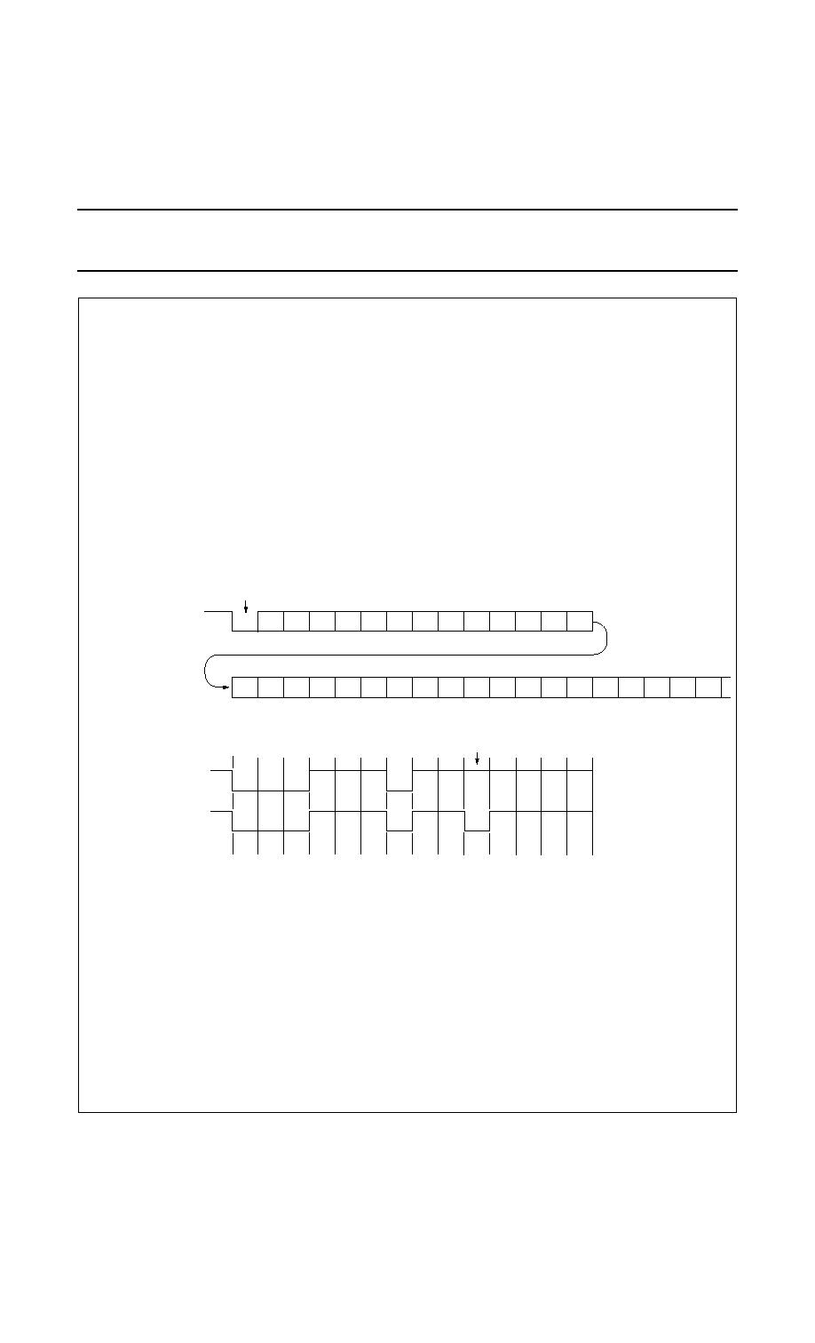
1999 Aug 19
44
Philips Semiconductors
Objective Specification
Single-chip 8-bit microcontroller with CAN controller
P8xC591
handbook, full pagewidth
MHI013
ID28
arbitration lost
ALC = 08
ID27 ID26 ID25 ID24 ID23 ID22 ID21 ID20 ID19 ID18 SRTR IDE
ID17 ID16 ID15 ID14 ID13 ID12 ID11 ID10 ID09 ID08 ID07 ID06 ID05
00
bit number:
standard and extended
frame messages:
extended
frame messages:
example:
TX
RX
01
02
03
04
05
06
07
08
09
10
11
12
13
bit number:
14
15
16
17
18
19
20
21
22
bit number:
00
01
02
03
04
05
06
07
08
23
24
25
ID04
26
ID03
27
ID02
28
ID01
29
ID00
30
RTR
31
start of frame
Fig.13 Arbitration Lost Bit Number Interpretation.

1999 Aug 19
45
Philips Semiconductors
Objective Specification
Single-chip 8-bit microcontroller with CAN controller
P8xC591
12.5.13 E
RROR
C
ODE
C
APTURE
(ECC)
This register contains information about the type and location of errors on the bus. The Error Code Capture Register
appears to the CPU as a read only memory.
Table 26 Error Code Capture (ECC) (CAN address 12)
Table 27 Description of Error Code Capture (ECC) Register 1 bits
Always if a bus error occurs, the corresponding bus error interrupt is forced, if enabled. In the same time, the current
position of the Bit Stream Processor is captured into the Error Code Capture Register. The content within this register is
fixed until the users software has read out its content once. From now on the capture mechanism is activated again.
The corresponding Interrupt Flag located in the Interrupt Register is cleared during the read access to the Interrupt
Register. A new Bus Error Interrupt is not possible until the Capture Register is read out once.
7
6
5
4
3
2
1
0
ERRC1
ERRC0
DIR
SEG4
SEG3
SEG2
SEG1
SEG0
BIT
SYMBOL
NAME
VALUE
FUNCTION
7
ERRC1
Error Code 1
ERRC1
ERRC0
6
ERRC0
Error Code 0
0
0
1
1
0
1
0
1
Bit Error
Form Error
Stuff Error
Other Error
5
DIR
Direction
1 (RX)
0 (TX)
Error occurred during reception
Error occurred during transmission
4
SEG4
Segment 4
Reflects the current Frame Segment to determine between different error events:
3
SEG3
Segment 3
00011
Start Of Frame
2
SEG2
Segment 2
00010
ID28 ... ID21
1
SEG1
Segment 1
00110
ID20 ... ID18
0
SEG0
Segment 0
00100
00111
01111
01110
01100
01101
01001
01011
01010
01000
11000
11001
11011
11010
10010
10001
10110
00011
10111
11100
IDE Bit
ID17 ... ID13
ID12 ... ID5
ID4 ... ID0
RTR Bit
Reserved Bit 1
Reserved Bit 0
Data Length Code
Data Field
CRC Sequence
CRC Delimiter
Acknowledge Slot
Acknowledge Delimiter
End Of Frame
Intermission
Active Error Flag
Passive Error Flag
Tolerate Dom. Bits
Error Delimiter
Overload Flag

1999 Aug 19
46
Philips Semiconductors
Objective Specification
Single-chip 8-bit microcontroller with CAN controller
P8xC591
12.5.14 E
RROR
W
ARNING
L
IMIT
R
EGISTER
(EWLR)
The Error Warning Limit could be defined within this register. The default value (after hardware reset) is 96d. In Reset
Mode this register appears to the CPU as a read / write memory.
Table 28 Error Warning Limit Register (EWLR) (CAN address 13)
Note that a content change of the EWL-Register is possible only, if the Reset Mode was entered previously. An Error
Status change (Status Register) and an Error Warning Interrupt forced by the new register content will not occur, until
the Reset Mode is cancelled again.
12.5.15 RX E
RROR
C
OUNTER
R
EGISTER
(RXERR)
The RX Error Counter Register reflects the current value of the Receive Error Counter. After hardware reset this register
is initialised to "0". In Operating Mode this register appears to the CPU as a read only memory. A write access to this
register is possible only in Reset Mode.
If a Bus Off event occurs, the RX Error counter is initialised to "0". As long as Bus Off is valid, writing to this register has
no effect.
Table 29 RX Error Counter Register (RXERR) (CAN address 14)
Note that a CPU-forced content change of the RX Error Counter is possible only, if the Reset Mode was entered
previously. An Error Status change (Status Register), an Error Warning or an Error Passive Interrupt forced by the new
register content will not occur, until the Reset Mode is cancelled again.
7
6
5
4
3
2
1
0
EWL.7
EWL.6
EWL.5
EWL.4
EWL.3
EWL.2
EWL.1
EWL.0
7
6
5
4
3
2
1
0
RXERR.7
RXERR.6
RXERR.5
RXERR.4
RXERR.3
RXERR.2
RXERR.1
RXERR.0

1999 Aug 19
47
Philips Semiconductors
Objective Specification
Single-chip 8-bit microcontroller with CAN controller
P8xC591
12.5.16 TX E
RROR
C
OUNTER
R
EGISTER
(TXERR)
The TX Error Counter Register reflects the current value of
the Transmit Error Counter. In Operating Mode this
register appears to the CPU as a read only memory. A
write access to this register is possible only in Reset Mode.
After hardware reset this register is initialised to "0". If a
bus-off event occurs, the TX Error Counter is initialised to
127 to count the minimum protocol-defined time (128
occurrences of the Bus-Free signal). Reading the TX Error
Counter during this time gives information about the status
of the Bus-Off recovery.
If Bus Off is active, a write access to TXERR in the range
of 0 to 254 clears the Bus Off Flag and the controller will
wait for one occurrence of 11 consecutive recessive bits
(bus free) after clearing of Reset Mode.
Writing 255 to TXERR allows to initiate a CPU-driven Bus
Off event. Note, that a CPU-forced content change of the
TX Error Counter is possible only, if the Reset Mode was
entered previously. An Error or Bus Status change (Status
Register), an Error Warning or an Error Passive Interrupt
forced by the new register content will not occur, until the
Reset Mode is cancelled again. After leaving the Reset
Mode, the new TX Counter content is interpreted and the
Bus Off event is performed in the same way, as if it was
forced by a bus error event. That means, that the Reset
Mode is entered again, the TX Error Counter is initialised
to 127, the RX Counter is cleared and all concerned Status
and Interrupt Register Bits are set.
Clearing of Reset Mode now will perform the protocol
defined Bus Off recovery sequence (waiting for 128
occurrences of the Bus-Free signal).
If the Reset Mode is entered again before the end of Bus
Off recovery (TXERR > 0), Bus Off keeps active and
TXERR is frozen.
Table 30 TX Error Counter Register (TXERR) (CAN address 15)
7
6
5
4
3
2
1
0
TXERR.7
TXERR.6
TXERR.5
TXERR.4
TXERR.3
TXERR.2
TXERR.1
TXERR.0
12.5.17 A
CCEPTANCE
F
ILTER
With the help of the Acceptance Filter the CAN Controller
is able to allow passing of received messages to the
RXFIFO only when the identifier bits and the Frame Type
of the received message are equal to the predefined ones
within the Acceptance Filter Registers. If at least one filter
matches, the message is copied to the receive FIFO.
The Acceptance Filter is defined by the Acceptance Code
Registers (ACRn) and the Acceptance Mask Registers
(AMRn). Within the Acceptance Code Registers the bit
patterns of messages to be received are defined. The
corresponding Acceptance Mask Registers allow defining
certain bit positions to be "don`t care".
The PeliCAN is designed to support four of so called
Acceptance Filter Banks. Each bank has the functionality
known from the SJA1000 with the extension, that a filter
change is possible "on the fly". Additionally the used
Frame Format of each filter bank is programmable now.

1999 Aug 19
48
Philips Semiconductors
Objective Specification
Single-chip 8-bit microcontroller with CAN controller
P8xC591
Fig.14 Acceptance Filter Tables.
handbook, full pagewidth
MHI014
ACCEPTANCE FILTER
BANK 4
ACR 0
MFORMATB4
AMODEB4
MFORMATB3
AMODEB3
MFORMATB2
ACCEPTANCE FILTER MODE REGISTER
AMODEB2
MFORMATB1
AMODEB1
B4F2EN
B4F1EN
B3F2EN
B3F1EN
B2F2EN
ACCEPTANCE FILTER ENABLE REGISTER
B2F1EN
B1F2EN
B1F1EN
dual/single
standard/
extended
ACR 1
ACR 2
ACR 3
AMR 0
AMR 1
AMR 2
AMR 3
ACCEPTANCE FILTER
BANK 3
ACR 0
ACR 1
ACR 2
ACR 3
AMR 0
AMR 1
AMR 2
AMR 3
ACCEPTANCE FILTER
BANK 2
ACR 0
ACR 1
ACR 2
ACR 3
AMR 0
AMR 1
AMR 2
AMR 3
ACCEPTANCE FILTER
BANK 1
ACR 0
ACR 1
ACR 2
ACR 3
AMR 0
AMR 1
AMR 2
AMR 3
dual/single
standard/
extended
dual/single
standard/
extended
dual/single
standard/
extended
filter 2
enable/
disable
filter 2
enable/
disable
filter 1
enable/
disable
filter 1
enable/
disable
filter 2
enable/
disable
filter 1
enable/
disable
filter 2
enable/
disable
filter 1
enable/
disable
B4F2PRIO
B4F1PRIO
B3F2PRIO
B3F1PRIO
B2F2PRIO
ACCEPTANCE FILTER PRIORITY REGISTER
B2F1PRIO
B1F2PRIO
B1F1PRIO
filter 2
priority
low/high
filter 2
priority
low/high
filter 1
priority
low/high
filter 1
priority
low/high
filter 2
priority
low/high
filter 1
priority
low/high
filter 2
priority
low/high
filter 1
priority
low/high

1999 Aug 19
49
Philips Semiconductors
Objective Specification
Single-chip 8-bit microcontroller with CAN controller
P8xC591
12.5.17.1 Acceptance Filter Mode Register
The current operating mode is defined within the Acceptance Filter Mode Register located at CAN Address 29. A write
access to this register is possible only within Reset Mode (Mode Register).
Note, that some bits are implemented only in case of the corresponding acceptance filter bank is implemented.
Not implemented bits are read as "0".
Table 31 Acceptance Filter Mode Register (ACF Mode) (CAN address 29)
7
6
5
4
3
2
1
0
MFORMATB4
AMODEB4
MFORMATB3
AMODEB3
MFORMATB2
AMODEB2
MFORMATB1
AMODEB1
Table 32 Acceptance Filter Mode Register (ACF Mode) 1 bits
BIT
SYMBOL
NAME
VALUE
FUNCTION
ACFMOD.7
MFORMATB4 Acceptance Filter
Format Bank 4
1 (EFF)
Acceptance Filter Bank 4 is used for Extended Frame
Messages only, Standard Frame Messages are ignored
0 (SFF)
Acceptance Filter Bank 4 is used for Standard Frame
Messages only, Extended Frame Messages are ignored
ACFMOD.6
AMODEB4
Acceptance Filter
Mode Bank 4
1 (single)
The Single Acceptance Filter option is enabled for filter
bank 4, -> one long filter is active
0 (dual)
The Dual Acceptance Filter option is enabled for filter
bank 4, -> two short filters are active
ACFMOD.5
MFORMATB3 Acceptance Filter
Format Bank 3
1 (EFF)
Acceptance Filter Bank 3 is used for Extended Frame
Messages only, Standard Frame Messages are ignored
0 (SFF)
Acceptance Filter Bank 3 is used for Standard Frame
Messages only, Extended Frame Messages are ignored
ACFMOD..4
AMODEB3
Acceptance Filter
Mode Bank 3
1 (single)
The Single Acceptance Filter option is enabled for filter
bank 3, -> one long filter is active
0 (dual)
The Dual Acceptance Filter option is enabled for filter
bank 3, -> two short filters are active
ACFMOD.3
MFORMATB2 Acceptance Filter
Format Bank 2
1 (EFF)
Acceptance Filter Bank 2 is used for Extended Frame
Messages only, Standard Frame Messages are ignored.
0 (SFF)
Acceptance Filter Bank 2 is used for Standard Frame
Messages only, Extended Frame Messages are
ignored.
ACFMOD.2
AMODEB2
Acceptance Filter
Mode Bank 2
1 (single)
The Single Acceptance Filter option is enabled for filter
bank 2, -> one long filter is active
0 (dual)
The Dual Acceptance Filter option is enabled for filter
bank 2, -> two short filters are active
ACFMOD.1
MFORMATB1 Acceptance Filter
Format Bank 1
1 (EFF)
Acceptance Filter Bank 1 is used for Extended Frame
Messages only, Standard Frame Messages are ignored
0 (SFF)
Acceptance Filter Bank 1 is used for Standard Frame
Messages only, Extended Frame Messages are ignored
ACFMOD.0
AMODEB1
Acceptance Filter
Mode Bank 1
1 (single)
The Single Acceptance Filter option is enabled for filter
bank 1, -> one long filter is active
0 (dual)
The Dual Acceptance Filter option is enabled for filter
bank 1, -> two short filters are active

1999 Aug 19
50
Philips Semiconductors
Objective Specification
Single-chip 8-bit microcontroller with CAN controller
P8xC591
12.5.17.2 Acceptance Filter Enable Register
Each defined Acceptance Filter is enabled or disabled by a certain bit located within the Acceptance Filter Enable
Register. This allows to change the Acceptance Filter Contents "on the fly" during normal operation if the corresponding
filter is disabled previously. A disabled Acceptance Filter does not allow passing of messages to the receive buffer. If all
Acceptance Filters are disabled (default after hardware reset) no messages will pass to the receive buffer at all.
The Acceptance Code and Mask registers are writable only, if the related Acceptance Filter is disabled or the CAN Block
is in Reset Mode.
Note, that some bits are implemented only in case of the corresponding acceptance filter bank is implemented.
Not implemented bits are read as "0".
Table 33 Acceptance Filter Enable Register (ACF Enable) (CAN address 30)
7
6
5
4
3
2
1
0
B4F2EN
B4F1EN
B3F2EN
B3F1EN
B2F2EN
B2F1EN
B1F2EN
B1F1EN
Table 34 Acceptance Filter Enable Register (ACF Enable)
Note, if the Single Filter Mode is selected for an Acceptance Filter Bank, this single filter is related to the corresponding
Filter 1 Enable Bit. The Filter 2 Enable Bits have no influence within Single Filter Mode.
BIT
SYMBOL
NAME
VALUE
FUNCTION
ACFEN.7
B4F2EN
Bank 4 Filter 2
Enable
1 (enabled) Filter 2 of Bank 4 is enabled, no write access to
corresponding Mask and Code Registers is possible
0 (disabled) Filter 2 of Bank 4 is enabled, changing of corresponding
Mask and Code Registers is possible.
ACFEN.6
B4F1EN
Bank 4 Filter 1
Enable
1 (enabled) Filter 1 of Bank 4 is enabled, no write access to
corresponding Mask and Code Registers is possible
0 (disabled) Filter 1 of Bank 4 is enabled, changing of corresponding
Mask and Code Registers is possible.
ACFEN.5
B3F2EN
Bank 3 Filter 2
Enable
1 (enabled) Filter 2 of Bank 3 is enabled, no write access to
corresponding Mask and Code Registers is possible
0 (disabled) Filter 2 of Bank 3 is enabled, changing of corresponding
Mask and Code Registers is possible.
ACFEN.4
B3F1EN
Bank 3 Filter 1
Enable
1 (enabled) Filter 1 of Bank 3 is enabled, no write access to
corresponding Mask and Code Registers is possible
0 (disabled) Filter 1 of Bank 3 is enabled, changing of corresponding
Mask and Code Registers is possible.
ACFEN.3
B2F2EN
Bank 2 Filter 2
Enable
1 (enabled) Filter 2 of Bank 2 is enabled, no write access to
corresponding Mask and Code Registers is possible
0 (disabled) Filter 2 of Bank 2 is enabled, changing of corresponding
Mask and Code Registers is possible.
ACFEN.2
B2F1EN
Bank 2 Filter 1
Enable
1 (enabled) Filter 1 of Bank 2 is enabled, no write access to
corresponding Mask and Code Registers is possible
0 (disabled) Filter 1 of Bank 2 is enabled, changing of corresponding
Mask and Code Registers is possible.
ACFEN.1
B1F2EN
Bank 1 Filter 2
Enable
1 (enabled) Filter 2 of Bank 1 is enabled, no write access to
corresponding Mask and Code Registers is possible
0 (disabled) Filter 2 of Bank 1 is enabled, changing of corresponding
Mask and Code Registers is possible.
ACFEN.0
B1F1EN
Bank 1 Filter 1
Enable
1 (enabled) Filter 1 of Bank 1 is enabled, no write access to
corresponding Mask and Code Registers is possible
0 (disabled) Filter 1 of Bank 1 is enabled, changing of corresponding
Mask and Code Registers is possible.

1999 Aug 19
51
Philips Semiconductors
Objective Specification
Single-chip 8-bit microcontroller with CAN controller
P8xC591
12.5.17.3 Acceptance Filter Priority Register
For each available Acceptance Filter it could be defined, whether a receive interrupt is forced immediately if a message
passes a certain Acceptance Filter or whether the programmed Receive Interrupt Level should be used for interruption.
This allows to use certain Acceptance Filters for alarm message recognition interrupting the host CPU immediately.
Note, that some bits are implemented only in case of the corresponding acceptance filter bank is implemented.
Not implemented bits are read as "0".
Table 35 Acceptance Filter Priority Register (ACF Priority) (CAN address 31)
7
6
5
4
3
2
1
0
B4F2PRIO
B4F1PRIO
B3F2PRIO
B3F1PRIO
B2F2PRIO
B2F1PRIO
B1F2PRIO
B1F1PRIO
Table 36 Acceptance Filter Priority Register (ACF Priority)
BIT
SYMBOL
NAME
VALUE
FUNCTION
ACFPRIO.7
B4F2PRIO Bank 4 Filter 2
Priority
1 (high)
A receive interrupt is generated immediately, if a message
passes Filter 2 within Acceptance Filter Bank 4
0 (low)
A receive interrupt is generated, if the FIFO level exceeds
the Receive Interrupt Level Register.
ACFPRIO.6
B4F1PRIO Bank 4 Filter 1
Priority
1 (high)
A receive interrupt is generated immediately, if a message
passes Filter 1 within Acceptance Filter Bank 4
0 (low)
A receive interrupt is generated, if the FIFO level exceeds
the Receive Interrupt Level Register.
ACFPRIO.5
B3F2PRIO Bank 3 Filter 2
Priority
1 (high)
A receive interrupt is generated immediately, if a message
passes Filter 2 within Acceptance Filter Bank 3
0 (low)
A receive interrupt is generated, if the FIFO level exceeds
the Receive Interrupt Level Register.
ACFPRIO.4
B3F1PRIO Bank 3 Filter 1
Priority
1 (high)
A receive interrupt is generated immediately, if a message
passes Filter 1 within Acceptance Filter Bank 3
0 (low)
A receive interrupt is generated, if the FIFO level exceeds
the Receive Interrupt Level Register.
ACFPRIO.3
B2F2PRIO Bank 2Filter 2
Priority
1 (high)
A receive interrupt is generated immediately, if a message
passes Filter 2 within Acceptance Filter Bank 2
0 (low)
A receive interrupt is generated, if the FIFO level exceeds
the Receive Interrupt Level Register.
ACFPRIO.2
B2F1PRIO Bank 2 Filter 1
Priority
1 (high)
A receive interrupt is generated immediately, if a message
passes Filter 1 within Acceptance Filter Bank 2
0 (low)
A receive interrupt is generated, if the FIFO level exceeds
the Receive Interrupt Level Register.
ACFPRIO.1
B1F2PRIO Bank 1 Filter 2
Priority
1 (high)
A receive interrupt is generated immediately, if a message
passes Filter 2 within Acceptance Filter Bank 1
0 (low)
A receive interrupt is generated, if the FIFO level exceeds
the Receive Interrupt Level Register.
ACFPRIO.0
B1F1PRIO Bank 1 Filter 1
Priority
1 (high)
A receive interrupt is generated immediately, if a message
passes Filter 1 within Acceptance Filter Bank 1
0 (low)
A receive interrupt is generated, if the FIFO level exceeds
the Receive Interrupt Level Register.
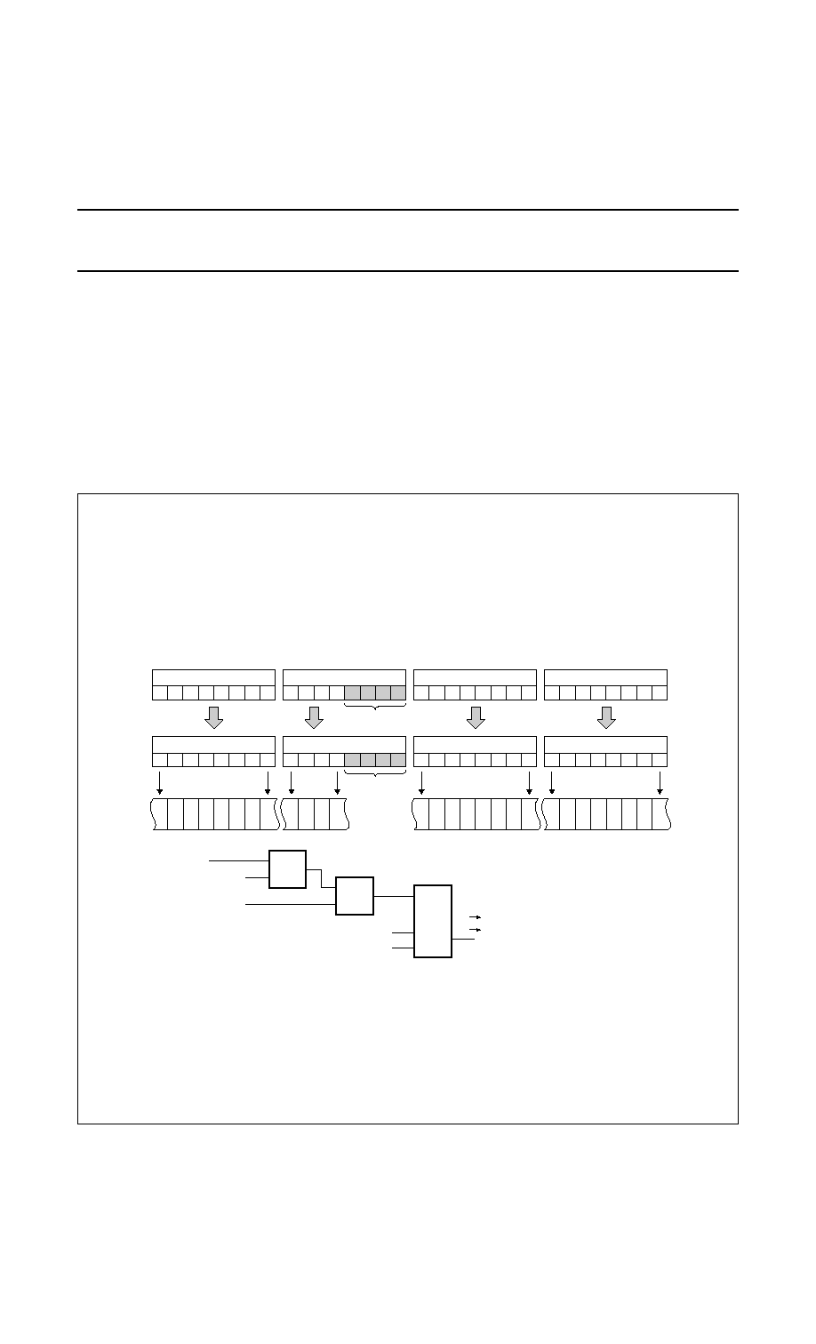
1999 Aug 19
52
Philips Semiconductors
Objective Specification
Single-chip 8-bit microcontroller with CAN controller
P8xC591
12.5.17.4 Single Filter Configuration
In this filter configuration one long filter (4-byte) could be
defined. The bit correspondences between the filter bytes
and the Message bytes depends on the programmed
Frame Format (see ACF Mode Register).
Single Filter Standard Frame:
If the Standard Frame Format is selected, the complete
Identifier including the RTR bit and the first two data bytes
are used for acceptance filtering. Messages may also be
accepted if there are no data bytes existing due to a set
RTR bit or if there is no or only one data byte because of
the corresponding data length code.
For a successful reception of a message, all single bit
comparisons have to signal acceptance. Note that the 4
least significant bits of AMR1 and ACR1 are not used. In
order to keep compatible with future products these bits
should be programmed to be "don`t care" by setting
AMR1.3, AMR1.2, AMR1.1 and AMR1.0 to "1".
Fig.15 Single Filter Configuration, receiving Standard Frame Messages.
handbook, full pagewidth
Addr.: 16
ACR0
7
6
5
4
3
2
1
0
MSB
LSB
Addr.: 18
ACR2
7
6
5
4
3
2
1
0
MSB
LSB
Addr.: 19
ACR3
7
6
5
4
3
2
1
0
MSB
LSB
Addr.: 17
ACR1
7
6
5
4
3
2
1
0
MSB
LSB
unused
Addr.: 20
AMR0
7
6
5
4
3
2
1
0
ID.28
ID.27
ID.26
ID.25
ID.24
ID.23
ID.22
MSB
LSB
Addr.: 22
AMR2
7
6
5
4
3
2
1
0
MSB
LSB
Addr.: 23
AMR3
7
6
5
4
3
2
1
0
MSB
LSB
Addr.: 21
AMR1
7
6
5
4
3
2
1
0
MSB
LSB
unused
ID.21
DB1.7
DB1.6
DB1.5
DB1.4
DB1.3
DB1.2
DB1.1
DB1.0
DB2.7
DB2.6
DB2.5
DB2.4
DB2.3
DB2.2
DB2.1
DB2.0
ID.20
ID.19
ID.18
RTR
&
[6]
[7]
0
1
not accepted
accepted
1
[0]
=
Message Bit
Acceptance Code Bit
Acceptance Mask Bit
DBx.y = Data Byte x, Bit y
MHI015

1999 Aug 19
53
Philips Semiconductors
Objective Specification
Single-chip 8-bit microcontroller with CAN controller
P8xC591
Single Filter Extended Frame:
If the Extended Frame Format is selected, the complete
Identifier including the RTR bit is used for acceptance
filtering.
For a successful reception of a message, all single bit
comparisons have to signal acceptance. Note that the 2
least significant bits of AMR3 and ACR3 are not used. In
order to keep compatible with future products these bits
should be programmed to be "don`t care" by setting
AMR3.1 and AMR3.0 to "1".
Fig.16 Single Filter Configuration, receiving Extended Frame Messages.
handbook, full pagewidth
Addr.: 16
ACR0
7
6
5
4
3
2
1
0
MSB
LSB
Addr.: 18
ACR2
7
6
5
4
3
2
1
0
MSB
LSB
Addr.: 19
ACR3
7
6
5
4
3
2
1
0
MSB
LSB
Addr.: 17
ACR1
7
6
5
4
3
2
1
0
MSB
LSB
unused
Addr.: 20
AMR0
7
6
5
4
3
2
1
0
ID.28
ID.27
ID.26
ID.25
ID.24
ID.23
ID.22
MSB
LSB
Addr.: 22
AMR2
7
6
5
4
3
2
1
0
MSB
LSB
Addr.: 23
AMR3
7
6
5
4
3
2
1
0
MSB
LSB
Addr.: 21
AMR1
7
6
5
4
3
2
1
0
MSB
LSB
unused
ID.21
ID.20
ID.19
ID.18
ID.17
ID.16
ID.15
ID.14
ID.13
ID.12
ID.11
ID.10
ID.9
ID.8
ID.7
ID.6
ID.5
ID.2
ID.3
ID.4
ID.1
ID.0
RTR
&
[6]
[7]
0
1
not accepted
accepted
1
[0]
=
Message Bit
Acceptance Code Bit
Acceptance Mask Bit
MHI016

1999 Aug 19
54
Philips Semiconductors
Objective Specification
Single-chip 8-bit microcontroller with CAN controller
P8xC591
12.5.17.5 Dual Filter Configuration
In this filter configuration two short filters could be defined.
A received message is compared with both filters to
decide, whether this message should be copied into the
Receive Buffer or not. If at least one of the filters signals an
acceptance, the received message becomes valid. The bit
correspondences between the filter bytes and the
message bytes depends on the currently received Frame
Format.
Dual Filter Standard Frame:
If the Standard Frame Format is selected, the two defined
filters are different. The first filter compares the complete
Standard Identifier including the RTR bit and the first Data
Byte of the message. The second filter just compares the
complete Standard Identifier including the RTR bit.
Fig.17 Dual Filter Configuration, receiving Standard Frame Messages.
handbook, full pagewidth
Addr.: 16
ACR0
7
6
5
4
3
2
1
0
MSB
LSB
ACR1
3
2
1
0
LSB
ACR3
3
2
1
0
LSB
Addr.: 17
7
6
5
4
MSB
ID.28
ID.27
ID.26
ID.25
ID.24
ID.23
ID.22
ID.21
ID.20
ID.19
ID.18
RTR
DB1.7
DB1.6
DB1.5
DB1.4
DB1.1
DB1.2
DB1.3
DB1.0
Addr.: 20
AMR0
7
6
5
4
3
2
1
0
MSB
LSB
AMR1
3
2
1
0
LSB
AMR3
3
2
1
0
LSB
Addr.: 21
7
6
5
4
MSB
[6]
[7]
1
1
[0]
[0]
1
=
Acceptance Code Bit
Acceptance Mask Bit
Filter 1
Filter 2
Filter 1
Filter 2
Message
Addr.: 22
AMR2
7
6
5
4
3
2
1
0
MSB
LSB
Addr.: 23
AMR3
7
6
5
4
MSB
Addr.: 18
ACR2
7
6
5
4
3
2
1
0
MSB
LSB
Addr.: 19
ACR3
7
6
5
4
MSB
. . .
. . .
. . .
.
.
.
[6]
[7]
0
1
not accepted
accepted
=
Message Bit
Acceptance Code Bit
Acceptance Mask Bit
. . .
. . .
. . .
.
.
.
&
&
MHI017
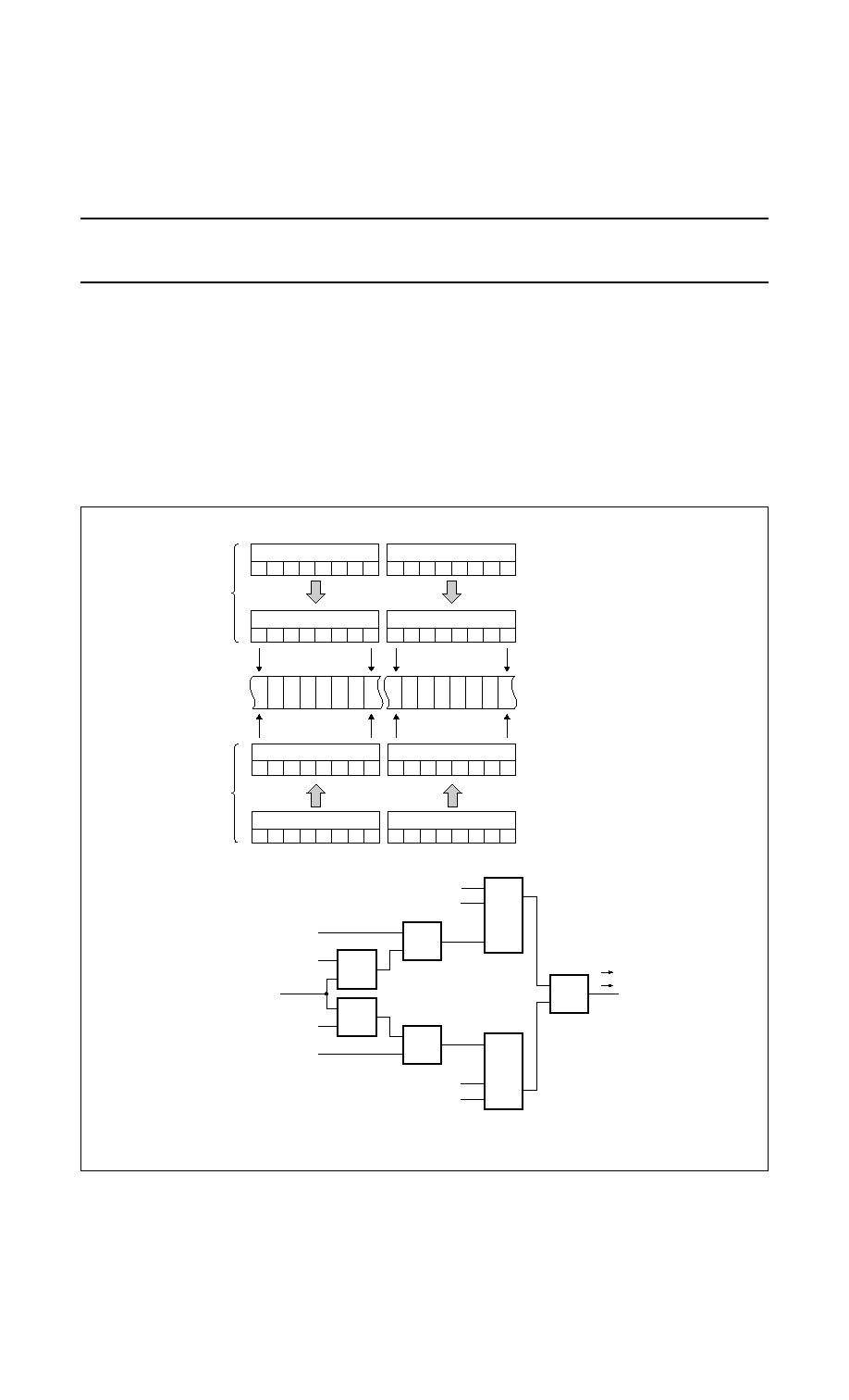
1999 Aug 19
55
Philips Semiconductors
Objective Specification
Single-chip 8-bit microcontroller with CAN controller
P8xC591
For a successful reception of a message, all single bit
comparisons of at least one complete filter have to signal
acceptance. In case of a set RTR bit or a data length code
of "0" no data byte is existing. Nevertheless, a message
may pass Filter 1, if the first part up to the RTR bit signals
acceptance.
If no data byte filtering is required for Filter 1, the four least
significant bits of AMR1 and AMR3 have to be set "1"
(don`t care). Then both filters are working identically using
the standard identifier range including the RTR bit.
Dual Filter Extended Frame:
If the Extended Frame Format is selected, the two defined
filters are looking identically. Both filters are comparing the
first two bytes of the Extended Identifier range only.
For a successful reception of a message, all single bit
comparisons of at least one complete filter have to signal
acceptance.
Fig.18 Dual Filter Configuration, receiving Extended Frame Messages.
handbook, full pagewidth
Addr.: 16
ACR0
7
6
5
4
3
2
1
0
MSB
LSB
ID.28
ID.27
ID.26
ID.25
ID.24
ID.23
ID.22
ID.21
ID.20
ID.19
ID.18
ID.17
ID.16
ID.15
ID.14
ID.13
Addr.: 20
AMR0
7
6
5
4
3
2
1
0
MSB
LSB
[6]
[7]
1
1
[0]
[0]
1
=
Acceptance Code Bit
Acceptance Mask Bit
Filter 1
Filter 2
Filter 1
Filter 2
Message
Addr.: 22
AMR2
7
6
5
4
3
2
1
0
MSB
LSB
Addr.: 23
AMR3
Addr.: 18
ACR2
7
6
5
4
3
2
1
0
7
6
5
4
3
2
1
0
7
6
5
4
3
2
1
0
MSB
LSB
MSB
LSB
MSB
LSB
Addr.: 19
ACR3
. . .
. . .
. . .
.
.
.
[6]
[7]
0
1
not accepted
accepted
=
Message Bit
Acceptance Code Bit
Acceptance Mask Bit
. . .
. . .
. . .
.
.
.
&
&
MHI018
Addr.: 17
ACR1
6
7
5
4
3
2
1
0
MSB
LSB
Addr.: 21
AMR1
6
7
5
4
3
2
1
0
MSB
LSB

1999 Aug 19
56
Philips Semiconductors
Objective Specification
Single-chip 8-bit microcontroller with CAN controller
P8xC591
12.5.18 T
RANSMIT
B
UFFER
The global layout of the Transmit Buffer is shown in Fig.19.
One has to distinguish between the Standard Frame
Format (SFF) and the Extended Frame Format (EFF)
configuration. The transmit buffer allows the definition of
one transmit message with up to eight data bytes.
12.5.18.1 Transmit Buffer Layout
It is subdivided into Descriptor and Data Field where the
first byte of the Descriptor Field is the Frame Information
Byte (Frame Info). It describes the Frame Format (SFF or
EFF), Remote or Data Frame and the Data Length. Two
identifier bytes for SFF and four bytes for EFF messages
follow. The Data Field contains up to eight data bytes. The
Transmit Buffer has a length of 13 bytes and is located in
the CAN address range from 112 to 124.
Fig.19 Transmit Buffer Layout for Standard and Extended Frame Format configurations.
handbook, full pagewidth
MHI023
TX Frame information
Standard Frame Format (SFF)
112
CAN Address
TX Identifier 1
113
TX Identifier 2
114
TX Data byte 1
115
TX Data byte 2
116
TX Data byte 3
117
TX Data byte 4
118
TX Data byte 5
119
TX Data byte 6
120
TX Data byte 7
121
TX Data byte 8
122
unused
123
unused
124
TX Frame information
Extended Frame Format (EFF)
112
CAN Address
TX Identifier 1
113
TX Identifier 2
114
TX Identifier 3
115
TX Identifier 4
116
TX Data byte 1
117
TX Data byte 2
118
TX Data byte 3
119
TX Data byte 4
120
TX Data byte 5
121
TX Data byte 6
122
TX Data byte 7
123
TX Data byte 8
124

1999 Aug 19
57
Philips Semiconductors
Objective Specification
Single-chip 8-bit microcontroller with CAN controller
P8xC591
12.5.18.2 Descriptor Field of the Transmit Buffer
This configuration is chosen to be compatible with the Receive Buffer Layout (see Section 12.5.19.1).
The values marked with "( )" in the Transmit Buffer should be set to the values expected in the Receive Buffer for an easy
comparison, only when using the Self Reception facility, otherwise they are don't care.
Table 37 Frame Format (FF) and Remote Transmission Request (RTR) bits
BIT
VALUE
FUNCTION
FF
1 (EFF)
Extended Frame Format will be transmitted by the CAN Controller
0 (SFF)
Standard Frame Format will be transmitted by the CAN Controller
RTR
1 (remote)
Remote Frame will be transmitted by the CAN Controller
0 (data)
Data Frame will be transmitted by the CAN Controller
Fig.20 Bit Layout Transmit Buffer.
7
FF
6
RTR
5
(0)
4
(0)
3
DLC.3
2
DLC.2
1
DLC.1
0
DLC.0
6
RTR
5
(0)
4
(0)
3
DLC.3
2
DLC.2
1
DLC.1
0
DLC.0
Addr. 112
TX Frame Information
Addr. 112
TX Frame Information
Standard Frame Format (SFF)
Extended Frame Format (EFF)
7
ID.28
6
ID.27
5
ID.26
4
ID.25
3
ID.24
2
ID.23
1
ID.22
0
ID.21
Addr 113
TX Identifier 1
7
ID.20
6
ID.19
5
ID.18
4
(RTR)
3
(0)
2
(0)
1
(0)
0
(0)
Addr. 114
TX Identifier 2
7
ID.28
6
ID.27
5
ID.26
4
ID.25
3
ID.24
2
ID.23
1
ID.22
0
ID.21
Addr. 113
TX Identifier 1
7
ID.20
6
ID.19
5
ID.18
4
ID.17
3
ID.16
2
ID.15
1
ID.14
0
ID.13
Addr. 114
TX Identifier 2
7
ID.12
6
ID.11
5
ID.10
4
ID.9
3
ID.8
2
ID.7
1
ID.6
0
ID.5
Addr. 115
TX Identifier 3
7
ID.4
6
ID.3
5
ID.2
4
ID.1
3
ID.0
2
(RTR)
1
(0)
0
(0)
Addr. 116
TX Identifier 4
Meaning of the Transmit Buffer Bits:
ID.x
Identifier bit x
FF
Frame Format
RTR
Remote Transmission Request
DLC.x
Data Length Code bit x
X
don't care
0
don't care, but recommended to be
compatible to Receive Buffer
7
FF

1999 Aug 19
58
Philips Semiconductors
Objective Specification
Single-chip 8-bit microcontroller with CAN controller
P8xC591
12.5.18.3 Data Length Code (DLC)
The number of bytes in the Data Field of a message is
coded by the Data Length Code. At the start of a Remote
Frame transmission the Data Length Code is not
considered due to the RTR bit being `1' (remote). This
forces the number of transmitted/received data bytes to be
0. Nevertheless, the Data Length Code must be specified
correctly to avoid bus errors, if two CAN Controllers start a
Remote Frame transmission with the same identifier
simultaneously.
The range of the Data Byte Count is 0 to 8 bytes and is
coded as follows:
`
For reasons of compatibility no Data Length Code > 8
should be used. If a value greater than 8 is selected, 8
bytes are transmitted in the data frame with the Data
Length Code specified in DLC.
12.5.18.4 Identifier (ID)
In Standard Frame Format (SFF) the Identifier consists of
11 bits (ID.28 to ID.18) and in Extended Frame Format
(EFF) messages the identifier consists of 29 bits (ID.28 to
ID.0). ID.28 is the most significant bit, which is transmitted
first on the bus during the arbitration process. The
Identifier acts as the message's name, used in a receiver
for acceptance filtering, and also determines the bus
access priority during the arbitration process. The lower
the binary value of the Identifier the higher the priority. This
is due to the larger number of leading dominant bits during
arbitration.
12.5.18.5 Data Field
The number of transferred data bytes is defined by the
Data Length Code. The first bit transmitted is the most
significant bit of data byte 1 at address 115 (SFF) or
address 117 (EFF).
DataByteCount
8
DLC.3
4
DLC.2
2
DLC.1
DLC.0
+
◊
+
◊
+
◊
=

1999 Aug 19
59
Philips Semiconductors
Objective Specification
Single-chip 8-bit microcontroller with CAN controller
P8xC591
12.5.19 R
ECEIVE
B
UFFER
The global layout of the Receive Buffer is very similar to the Transmit Buffer described in the previous chapter. The
Receive Buffer is the accessible part of the RXFIFO and is located in the range between CAN Address 96 and 108. Each
message is subdivided into a Descriptor and a Data Field.
Fig.21 Example of the message storage within the RXFIFO.
Message 1 is now available in the Receive Buffer
Note that message 2 should not be read until it has been shifted to address 96 by a Release Receive
Buffer Command because this message may be in process now and due to this not fixed.
handbook, full pagewidth
MHI019
message 3
message 2
message 1
receive
buffer
window
incoming
messages
receive
FIFO
106
107
108
103
104
105
100
101
102
99
96
97
98

1999 Aug 19
60
Philips Semiconductors
Objective Specification
Single-chip 8-bit microcontroller with CAN controller
P8xC591
12.5.19.1 Descriptor File of the Receive Buffer
Identifier, Frame Format, Remote Transmission Request bit and Data Length Code have the same meaning as described
in the Transmit Buffer.
Fig.22 Bit Layout Receive Buffer.
7
ID.28
6
ID.27
5
ID.26
4
ID.25
3
ID.24
2
ID.23
1
ID.22
0
ID.21
7
ID.28
6
ID.27
5
ID.26
4
ID.25
3
ID.24
2
ID.23
1
ID.22
0
ID.21
Addr. 97
RX Identifier 1
Addr. 97
RX Identifier 1
Standard Frame Format (SFF)
Extended Frame Format (EFF)
7
ID.20
6
ID.19
5
ID.18
4
RTR
3
0
2
0
1
0
0
0
Addr. 98
RX Identifier 2
7
ID.20
6
ID.19
5
ID.18
4
ID.17
3
ID.16
2
ID.15
1
ID.14
0
ID.13
Addr. 98
RX Identifier 2
7
ID.12
6
ID.11
5
ID.10
4
ID.9
3
ID.8
2
ID.7
1
ID.6
0
ID.5
Addr. 99
RX Identifier 3
7
ID.4
6
ID.3
5
ID.2
4
ID.1
3
ID.0
2
RTR
1
0
0
0
Addr. 100
RX Identifier 4
Meaning of the Receive Buffer Bits:
ID.x
Identifier bit x
IDX.x
Index bit x
FF
Frame Format
RTR
Remote Transmission Request
DLC.x
Data Length Code bit x
7
FF
6
RTR
5
0
4
0
3
DLC.3
2
DLC.2
1
DLC.1
0
DLC.0
Addr. 96
RX Frame Information
7
FF
6
RTR
5
0
4
0
3
DLC.3
2
DLC.2
1
DLC.1
0
DLC.0
Addr. 96
RX Frame Information
Note:
The received Data Length Code located in the Frame
Information Byte represents the real sent Data Length
Code, which may be greater than 8 (depends on
transmitting CAN node). Nevertheless, the maximum
number of received data bytes is 8. This should be taken
into account by reading a message from the Receive
Buffer.
It depends on the data length how many CAN messages
can fit in the RXFIFO at one time. If there is not enough
space for a new message within the RXFIFO, the CAN
Controller generates a Data Overrun condition the
moment this message becomes valid and the acceptance
test was positive. A message that is partly written into the
RXFIFO, when the Data Overrun situation occurs, is
deleted. This situation is signalled to the CPU via the
Status Register and the Data Overrun Interrupt, if enabled.

1999 Aug 19
61
Philips Semiconductors
Objective Specification
Single-chip 8-bit microcontroller with CAN controller
P8xC591
13 SERIAL I/O
The P8xC591 is equipped with three independent serial
ports: CAN, SIO0 and SIO1. SIO0 is a Standard Serial
Interface UART with enhanced functionality. In following
there will be one Section describing the Standard UART
functionality and an extra Section for Enhanced UART.
SIO1 accommodates the I
2
C bus.
14 SIO0 STANDARD SERIAL INTERFACE UART
The serial port is full duplex, meaning it can transmit and
receive simultaneously. It is also receive-buffered,
meaning it can commence reception of a second byte
before a previously received byte has been read from the
register. (However, if the first byte still hasn't been read by
the time reception of the second byte is complete, one of
the bytes will be lost.) The serial port receive and transmit
registers are both accessed at Special Function Register
transmit registers are both accessed at Special Function
Register S0BUF. Writing to S0BUF loads the transmit
register, and reading S0BUF accesses a physically
separate receive register.
The serial port can operate in 4 modes (one synchronous
mode, three asynchronous modes). The baud rate clock
for the serial port is derived from the oscillator frequency
(mode 0, 2) or generated either by timer 1 or by dedicated
baud rate generator (mode 1, 3).
Mode 0 Shift Register (Synchronous) Mode:
Serial data enters and exits through RxD. TxD
outputs the shift clock. 8 bits are transmitted/
received (LSB first). The baud rate is fixed
1
/
6
the
oscillator frequency.
Mode 1 8-bit UART, Variable Baud Rate:
10 bits are transmitted (through TxD) or received
(through RxD): a start bit (0), 8 data bits (LSB
first), and a stop bit (1). On receive, the stop bit
goes into RB8 in Special Function Register
SCON. The baud rate is variable.
Mode 2 9-bit UART, Fixed Baud Rate:
11 bits are transmitted (through TxD) or received
(through RxD): start bit (0), 8 data bits (LSB first),
a programmable 9
th
data bit, and a stop bit (1).
On Transmit, the 9
th
data bit (TB8 in SCON) can
be assigned the value of 0 or 1. Or, for example,
the parity bit (P, in the PSW) could be moved into
TB8. On receive, the 9
th
data bit goes into RB8 in
Special Function Register SCON, while the stop
bit ignored. The baud rate is programmable to
either
1
/
16
or
1
/
32
the oscillator frequency.
Mode 3 9-bit UART, Variable Baud Rate:
11 bits are transmitted (through TxD) or received
(through RxD): start bit (0), 8 data bits (LSB first),
a programmable 9
th
data bit, and a stop bit (1). In
fact, Mode 3 is the same as Mode 2 in all respects
except baud rate. The baud rate in Mode 3 is
variable.
In all four modes, transmission is initiated by any
instruction that uses S0BUF as a destination register.
Reception is initiated in Mode 0 by the condition RI = 0 and
REN = 1. Reception is initiated in the other modes by the
incoming start bit if REN = 1.
14.1
Multiprocessor Communications
Modes 2 and 3 have a special provision for multiprocessor
communications. In these modes, 9 data bits are received.
The 9
th
one goes into RB8. Then comes a stop bit. The
port can be programmed such that when the stop bit is
received, the serial port interrupt will be activated only if
RB8 = 1. This feature is enabled by setting bit SM2 in
SCON. A way to use this feature in multiprocessor
systems is as follows:
When the master processor wants to transmit a block of
data to one of several slaves, it first send out an address
byte which indentifies the target slave. An address byte
differs from a data byte in that the 9
th
bit is 1 in an address
byte and 0 in a data byte. With SM2 = 1, no slave will be
interrupted by a data byte. An address byte, however, will
interrupt all slaves, so that each slave can examine the
received byte and see if it is being addressed. The
addressed slave will clear its SM2 bit and prepare to
receive the data bytes that will be coming. The slaves that
weren't being addressed leave their SM2s set and go on
about their business, ignoring the coming data bytes.
SM2 has no effect in Mode 0, and in Mode 1 can be used
to check the validity of the stop bit. In a Mode 1 reception,
if SM2 = 1, the receive interrupt will not be activated unless
a valid stop bit is received.
14.2
Serial Port Control Register
The serial port control and status register is the Special
Function Register SCON, shown in Table 38, 40 and 41.
This register contains not only the mode selection bits, but
also the 9
th
data bit for transmit and receive (TB8 and
RB8), and the serial port interrupt bits (TI and RI).
S0BUF is the receive and transmit buffer of serial
interface. Writing to S0BUF loads the transmit register and
initiates transmission. Reading out S0BUF accesses a
physically separate receive register.

1999 Aug 19
62
Philips Semiconductors
Objective Specification
Single-chip 8-bit microcontroller with CAN controller
P8xC591
14.3
Baud Rate Generation
There are several possibilities to generate the baud rate
clock for the serial port depending on the mode in which it
is operating.
For clarification some terms regarding the difference
between "baud rate clock" and "baud rate" should be
mentioned. The serial interface requires a clock rate which
is 16 times the baud rate for internal synchronization.
Therefore, the baud rate generators have to provide a
"baud rate clock" to the serial interface which - there
divided by 16 - results in the actual "baud rate". However,
all formulas given in the following section already include
the factor and calculate the final baud rate. Further, the
abbreviation f
CLK
refers to the external clock frequency
(oscillator or external input clock operation).
The baud rate of the serial port is controlled by the two bits
SPS and SMOD1 which are located in the Special
Function Registers S0PSH and PCON. In SFRs S0PSH
and S0PSL the prescaler load value of the internal baud
rate generator can be programmed (see Table 38 to 43).
14.3.1
I
NTERNAL
B
AUD
R
ATE
G
ENERATOR
P
RESCALER
S0PSH, S0PSL
Table 38 Internal Baud Rate Generator Prescaler Low Register S0PSL (address FAH)
Prescaler load value
Table 39 Description of S0PSL bits
Table 40 Internal Baud Rate Generator Prescaler High Register S0PSH (address FBH)
Prescaler higher nibble load value
Table 41 Description of S0PSH bits
14.3.2
PCON
FOR THE
I
NTERNAL
B
AUD
R
ATE
G
ENERATOR
Table 42 PCON (address 87H)
Prescaler load value
Table 43 Description of SMOD1 and SMOD0 bits
7
6
5
4
3
2
1
0
prescaler load value
BIT
SYMBOL
DESCRIPTION
7 to 0
-
Baud reload low value. Lower 8 bits of the baud rate timer reload value.
7
6
5
4
3
2
1
0
SPS
-
-
-
higher nibble load value
BIT
SYMBOL
DESCRIPTION
7
SPS
Baud rate generator enable. When set, the baud rate of serial interface is derived from
the dedicated baud rate generator. When cleared (default after reset), baud rate is derived
from the Timer 1 overflow rate.
6 to 4
-
Reserved.
3 to 0
-
Baud rate generator reload high value. Upper four bits of the baud rate timer value.
7
6
5
4
3
2
1
0
SMOD1
SMOD0
(POF)
(WLE)
(GF1)
(GF0)
(PD)
(IDL)
BIT
SYMBOL
DESCRIPTION
7
SMOD1
Double Baud rate. When set, the baud rate of serial interface is modes 1, 2, 3 is
doubled. After reset this bit is cleared.
6
SMOD0
Double Baud rate. Selects SM0/FE for SCON.7 bit.
5 to 0
(POF) to (IDL) Description refer to Section 11.3.5 "Power Control Register (PCON)".

1999 Aug 19
63
Philips Semiconductors
Objective Specification
Single-chip 8-bit microcontroller with CAN controller
P8xC591
14.3.3
B
AUD
R
ATE
G
ENERATION
O
VERVIEW
O
F
O
PTIONS
Depending on the programmed operating mode different paths are selected for the baud rate clock generation. Figure 23
shows the dependencies of the serial port baud rate clock generation on the two control bits and from the mode which
is selected in the Special Function Register SCON:
Fig.23 Baud Rate Generation for the Serial Port.
Note: The switch configuration shows the reset state.
handbook, full pagewidth
MHI024
BAUD
RATE
GENERATOR
BAUD
RATE
CLOCK
˜
6
(S0PSH
S0PSL)
S0PSH.7
(SPS)
TIMER 1
overflow
fCLK
SCON.7
SCON.6
(SM0/FE)
mode 1
mode 3
only one
mode can be selected
mode 2
mode 0
0
1
PCON.7
(SMOD1)
0
1
˜
2

1999 Aug 19
64
Philips Semiconductors
Objective Specification
Single-chip 8-bit microcontroller with CAN controller
P8xC591
14.3.4
B
AUD
R
ATE IN
M
ODE
0
The baud rate in Mode 0 is fixed to:
14.3.5
B
AUD
R
ATE IN
M
ODE
2
The baud rate in Mode 2 depends on the value of bit
SMOD1 in Special Function Register PCON. If SMOD1 =
0 (which is the value after reset), the baud rate is
1
/
32
of
oscillator frequency. If SMOD1 = 1, the baud rate is
1
/
16
of
the oscillator frequency:
14.3.6
B
AUD
R
ATE IN
M
ODE
1
AND
3
In these modes the baud rate is variable and can be
generated alternatively by a baud rate generator or by
Timer 1.
Mode 0 baud rate
oscillator frequency
6
-------------------------------------------------------
=
Mode 2 baud rate
2
SMOD1
32
--------------------
oscillator frequency
◊
=
14.3.7
U
SING THE
I
NTERNAL
B
AUD
R
ATE
G
ENERATOR
In Modes 1 and 3, the P8xC591 can use an internal baud
rate generator for the serial port. To enable this feature, bit
SPS (bit 7 of Special Function Register S0PSH) must be
set. Bit SMOD1 (PCON.7) controls a divide-by-2 circuit
which affect the input and output clock signal of the baud
rate generator. After reset the divide-by-2 circuit is active
and the resulting overflow output clock will be divided by 2.
The input clock of the baud rate generator is f
CLK.
The baud rate generator consists of its own free running
upward counting 12-bit timer. On overflow of this timer
(next count step after counter value FFFH) there is an
automatic 12-bit reload from the registers S0PSL and
S0PSH. The lower 8 bits of the timer are reloaded from
S0PSL, while the upper four bits are reloaded from bit 0 to
3 of register S0PSH. The baud rate timer is reloaded by
writing to S0PSH.
Fig.24 Serial Port Input Clock when using the Baud Rate Generator.
Note: The switch configuration shows the reset state.
handbook, full pagewidth
MHI025
BAUD
RATE
CLOCK
BAUD RATE
fCLK
PCON.7
(SMOD1)
0
1
˜
2
12 BIT TIMER
S0PSH
S0PSL
overflow
input
clock
.3 .2 .1 .0

1999 Aug 19
65
Philips Semiconductors
Objective Specification
Single-chip 8-bit microcontroller with CAN controller
P8xC591
With the baud rate generator as clock source for the serial
port in Mode 1 and Mode 3, the baud rate of can be
determined as follows:
Mode 1, 3 baud rate =
Baud rate generator overflow rate =
2
12
- S0PS with S0PS = S0PSH.3 - 0, S0PSL.7 - 0.
S0PS: Baud Rate Generator Prescaler load value
Table 47 lists baud rates and how they can be obtained
from the Internal Baud Rate Generator.
14.3.8
U
SING
T
IMER
1
TO
G
ENERATE
B
AUD
R
ATES
In Mode 1 and 3 of the serial port also timer 1 can be used
for generating baud rates. Then the baud rate is
determined by the timer 1 overflow rate and the value of
SMOD1 as follows:
2
SMOD1
osciillator frequency
◊
32
(baud rate generator overflow rate)
◊
---------------------------------------------------------------------------------------------------------
The Timer 1 interrupt is usually disabled in this application.
Timer 1 itself can be configured for either "timer" or
"counter" operation, and in any of its operating modes. In
most typical applications, it is configured for "timer"
operation in the auto-reload (high nibble of TMOD =
0010B). In this case the baud rate is given by the formula:
Very low baud rates can be achieved with Timer 1 if
leaving the Timer 1 interrupt enabled, configuring the timer
to run as 16-bit timer (high nibble of TMOD = 0001B), and
using the Timer 1 interrupt for a 16-bit software reload.
Table 48 lists lower baud rates and how they can be
obtained from Timer 1.
Mode 1, 3 baud rate
2
SMOD1
32
--------------------
(timer 1 overflow rate)
◊
=
Mode1 3 baud rate =
2
SMOD1
oscillator frequency
◊
32
6
256
TH1
(
)
≠
(
)
◊
◊
-------------------------------------------------------------------------------
,
Table 44 Serial Port Control Register SCON (address)
Table 45 Description of S0PSH and S0PSL bits
7
6
5
4
3
2
1
0
SM0
SM1
SM2
REN
TB8
RB8
TI
RI
BIT
SYMBOL
DESCRIPTION
7
SM0
See Table 46.
6
SM1
See Table 46.
5
SM2
Enables the multiprocessor communication feature in Modes 2 and 3. In Mode 2 or
3, if SM2 is set to 1, then RI will not be activated if the received 9
th
data bit (RB8) is 0. In
Mode 1, if SM2 = 1 then RI will not be activated if a valid stop bit was not received. In
Mode 0, SM2 should be 0.
4
REN
Enables serial reception. Set by software to enable reception. Clear by software to
disable reception.
3
TB8
The 9
th
data bit that will be transmitted in Modes 2 and 3. Set or clear by software as
desired.
2
RB8
In Modes 2 and 3, is the 9
th
data bit that was received. In Mode 1, if SM2 = 0, RB8 is
the stop bit that was received. In Mode 0, RB8 is not used.
1
TI
Transmit interrupt flag. Set by hardware at the end of the 8
th
bit time in Mode 0, or at
the beginning of the stop bit in the other modes, in any serial transmission. Must be
cleared by software.
0
RI
Receive interrupt flag. Set by hardware at the end of the 8
th
bit time in Mode 0, or
halfway through the stop bit time in the other modes, in any serial reception (except see
SM2). Must be cleared by software.

1999 Aug 19
66
Philips Semiconductors
Objective Specification
Single-chip 8-bit microcontroller with CAN controller
P8xC591
Table 46 Serial port mode select
Table 47 Internal baud rate timer generated baud rates
Table 48 Timer 1 generated baud rates
SM0
SM1
MODE
DESCRIPTION
BAUD RATE
0
0
Mode 0
Shift register
1
/
6
◊
f
CLK
0
1
Mode 1
8-bit UART
variable
1
0
Mode 2
9-bit UART
1
/
32
or
1
/
16
◊
f
CLK
1
1
Mode 3
9-bit UART
variable
BAUD RATE
(KBits/s)
f
CLK
(MHz)
SPS
SMOD1
INTERNAL BAUD RATE TIMER
DEVIATION %
MODE
RELOAD VALUE
1000
16
1
1
0
1/3
FFFh
750
12
1
1
0
1/3
FFFh
500
8
1
1
0
1/3
FFFh
250
8
1
0
0
1/3
FFFh
250
8
1
1
0
1/3
FFEh
38.4
8
1
1
0.16
1/3
FF3h
38.4
16
1
0
0.16
1/3
FF3h
19.2
4
1
1
0.16
1/3
FF3h
9.6
16
1
1
0.16
1/3
F98h
4.8
16
1
1
0.16
1/3
F30h
0.3
16
1
1
0.01
1/3
2FBh
0.11
8
1
0
-
0.01
1/3
71Fh
BAUD RATE
(KBits/s)
f
CLK
(MHz)
SPS
SMOD1
INTERNAL BAUD RATE TIMER
DEVIATION %
MODE
RELOAD VALUE
110
16
0
1
0.01
1
FA15h
110
12
0
0
0.03
1
FDC8h
110
4
0
1
-
0.06
1
FE85h
110
4
0
0
0.21
2
43h

1999 Aug 19
67
Philips Semiconductors
Objective Specification
Single-chip 8-bit microcontroller with CAN controller
P8xC591
14.4
More about UART Modes
More About Mode 0
Serial data enters and exits through RxD. TxD outputs the
shift clock. 8 bits are transmitted/received: 8 data bits (LSB
first). The baud rate is fixed a
1
/
6
the oscillator frequency.
Figure 25 shows a simplified functional diagram of the
serial port in Mode 0, and associated timing.
Transmission is initiated by any instruction that uses
S0BUF as a destination register. The "write to S0BUF"
signal at S6P2 also loads a 1 into the 9
th
position of the
transmit shift register and tells the TX Control block to
commence a transmission. The internal timing is such that
one full machine cycle will elapse between "write to
S0BUF" and activation of SEND.
SEND enables the output of the shift register to the
alternate output function line of P3.0 and also enable
SHIFT CLOCK to the alternate output function line of P3.1.
SHIFT CLOCK is low during S3, S4, and S5 of every
machine cycle, and high during S6, S1 and S2. At S6P2 of
every machine cycle in which SEND is active, the contents
of the transmit shift are shifted to the right one position.
As data bits shift out to the right, zeros come in from the
left. When the MSB of the data byte is at the output
position of the shift register, then the 1 that was initially
loaded into the 9
th
position, is just to the left of the MSB,
and all positions to the left of that contain zeros. This
condition flags the TX Control block to do one last shift and
then deactivate SEND and set T1. Both of these actions
occur at S1P1 of the 10
th
machine cycle after "write to
S0BUF".
Reception is initiated by the condition REN = 1 and
R1 = 0. At S6P2 of the next machine cycle, the RX Control
unit writes the bits 11111110 to the receive shift register,
and in the next clock phase activates RECEIVE.
RECEIVE enable SHIFT CLOCK to the alternate output
function line of P3.1. SHIFT CLOCK makes transitions at
S3P1 and S6P1 of every machine cycle. At S6P2 of every
machine cycle. At S6P2 of every machine cycle in which
RECEIVE is active, the contents of the receive shift
register are shifted to the left one position. The value that
comes in from the right is the value that was sampled at
the P3.0 pin at S5P2 of the same machine cycle.
As data bits come in from the right, 1s shift out to the left.
When the 0 that was initially loaded into the rightmost
position arrives at the leftmost position in the shift register,
it flags the RX Control block to do one last shift and load
S0BUF. At S1P1 of the 10
th
machine cycle after the write
to SCON that cleared RI, RECEIVE is cleared as RI is set.
More About Mode 1
Ten bits are transmitted (through TxD), or received
(through RxD): a start bit (0), 8 data bits (LSB first), and a
stop bit (1). On receive, the stop bit goes into RB8 in
SCON. In the 80C51 the baud rate is determined by the
Timer 1 overflow rate.
Figure 26 shows a simplified functional diagram of the
serial port in Mode1, and associated timings for transmit
receive.
Transmission is initiated by any instruction that uses
S0BUF as a destination register. The "write to S0BUF"
signal also loads a1 into the 9
th
bit position of the transmit
shift register and flags the TX Control unit that a
transmission is requested. Transmission actually
commences at S1P1 of the machine cycle following the
next rollover in the divide-by-16 counter. (Thus, the bit
times are synchronized to the divide-by-16 counter, not to
the "write to S0BUF" signal.)
The transmission begins with activation of SEND which
puts the start bit at TxD. One bit time later, DATA is
activated, which enables the output bit of the transmit shift
register to TxD. The first shift pulse occurs one bit time
after that.
As data bits shift out to the right, zeros are clocked in from
the left. When the MSB of the data byte is at the output
position of the shift register, then the 1 that was initially
loaded into the 9
th
position is just to the left of the MSB,
and all positions to the left of that contain zeros. The
condition flags the TX Control unit to do one last shift and
then deactivate SEND and set TI. This occurs at the 10
th
divide-by-16 rollover after "write to S0BUF".
Reception is initiated by a detected 1-to-0 transition at
RxD. For this purpose RxD is sampled at a rate of 16 times
whatever baud rate has been established. When a
transition is detected, the divide-by-16 counter is
immediately reset, and 1 FFH is written into the input shift
register. Resetting the divide-by-16 counter aligns its
rollovers with the boundaries of the incoming bit times.
The 16 states of the counter divide each bit time into 16
ths
.
At the 7
th
, 8
th
, and 9
th
counter states of each bit time, the
bit detector samples the value of RxD. The value accepted
is the value that was seen in at least 2 of the 3 samples.
This is done for noise rejection. If the value accepted
during the first bit time is not 0, the receive circuits are
reset and the unit goes back to looking for another 1-to-0
transition. This is to provide rejection of false start bits. If
the start bit proves valid, it shifted into the input shift
register, and reception of the rest of the frame will proceed.

1999 Aug 19
68
Philips Semiconductors
Objective Specification
Single-chip 8-bit microcontroller with CAN controller
P8xC591
As data bits come in from the right, 1s shift out to the left.
When the start bit arrives at the leftmost position in the shift
register (which in Mode 1 is a 9-bit register), it flags the RX
Control block to do one last shift, load S0BUF and RB8,
and set RI. The signal to load S0BUF and RB8, and to set
RI, will be generated if, and only if, the following conditions
are met at the time the final shift pulse is generated:
1. RI = 0, and
2. Either SM2 = 0, or the received stop bit = 1.
If either of these two conditions is not met, the received
frame is irretrievably lost. If both conditions are met, the
stop bit goes into RB8, the 8 data bits go into S0BUF, and
RI is activated. At this time, whether the above conditions
are met or not, the unit goes back to looking for a 1-to-0
transition in RxD.
More About Modes 2 and 3
Eleven bits are transmitted (through TxD), or received
(through RxD): a start bit (0), 8 data bits (LSB first), a
programmable 9
th
data bit, and a stop bit (1). On transmit,
the 9
th
data bit (TB8) can be assigned the values of 0 or 1.
On receive, the 9
the
data bit goes into RB8 in SCON. The
baud rate is programmable to either
1
/
16
or
1
/
32
the
oscillator frequency in Mode 2. Mode 3 may have a
variable baud rate generated from Timer 1.
Figure 27 show a functional diagram of the serial port in
Modes 2 and 3. The receive portion is exactly the same as
in Mode 1. The transmit portion differs from Mode 1 only in
the 9
th
bit of the transmit shift register.
Transmission is initiated by any instruction that uses
S0BUF as a destination register. The "write to S0BUF"
signal also loads TB8 into the 9
th
bit position of the transmit
shift register and flags the TX Control unit that a
transmission is requested. Transmission commences at
S1P1 of the machine cycle following the next rollover in the
divide-by-16 counter. (Thus, the bit times are
synchronized to the divide-by-16 counter, not to the "write
to SUB" signal).
The transmission begins with activation of SEND, which
puts the start bit at TxD. One bit time later, DATA is
activated, which enables the output bit of the transmit shift
register to TxD. The first shift pulse occurs one bit time
after that. The first shift clocks a 1 (the stop bit) into the 9
th
bit position of the shift register. Thereafter, only zeros are
clocked in. Thus, as data bit shift out to the right, zeros are
clocked in from the left. When TB8 is at the output position
of the shift register, then the stop bit is just to the left of
TB8, and all positions to the left of that contain zeros.
This condition flags the TX Control unit to do one last shift
and then deactivate SEND and set TI. This occurs at the
11
th
divide-by-16 rollover after "write to SUBF".
Reception is initiated by a detected 1-to-0 transition at
RxD. For this purpose RxD is sampled at a rate of 16 times
whatever baud rate has been established. When a
transition is detected, the divide-by-16 counter is
immediately reset, and 1FFH is written to the input shift
register.
At the 7
th
, 8
th
, and 9
th
counter states of each bit time, the
bit detector samples the value of R-D. The value accepted
is the value that was seen in at least 2 of the 3 samples. If
the value accepted during the first bit time is not 0, the
receive circuits are reset and the unit goes back to looking
for another 1-to-0 transition. If the start bit proves valid, it
is shifted into the input shift register, and reception of the
rest of the frame will proceed.
As data bits come in from the right, 1s shift out to the left.
When the start bit arrives at the leftmost position in the shift
register (which in Modes 2 and 3 is a 9-bit register), it flags
the RX Control block to do one last shift, load S0BUF and
RB8, and set RI.
The signal to load S0BUF and RB8, and to set RI, will be
generated if, and only if, the following conditions are met
at the time the final shift pulse is generated.
1. RI = 0, and
2. Either SM2 = 0, or the received 9
th
data bit = 1.
If either of these conditions is not met, the received frame
is irretrievably lost, and RI is not set. If both conditions are
met, the received 9
th
data bit goes into RB8, and the first 8
data bits go into S0BUF. One bit time later, whether the
above conditions were met or not, the unit goes back to
looking for a 1-to-0 transition at the RxD input.
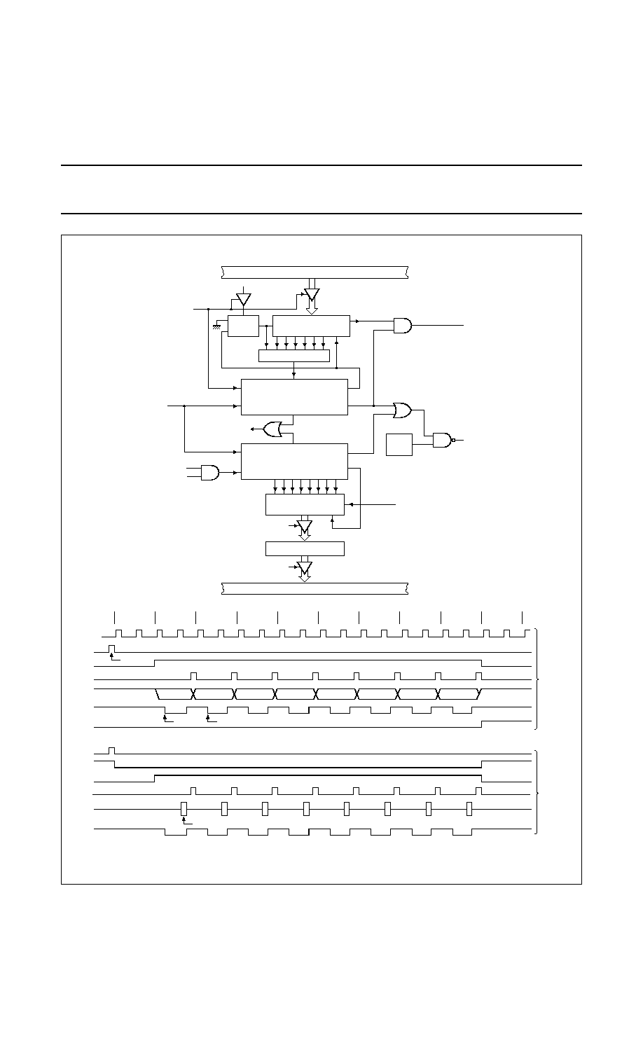
1999 Aug 19
69
Philips Semiconductors
Objective Specification
Single-chip 8-bit microcontroller with CAN controller
P8xC591
Fig.25 Serial Port Mode 0.
handbook, full pagewidth
SBUF
TX CONTROL
T1
Start
TX Clock
Shift
Send
S
write to SBUF
serial port interrupt
S6
Q
D
CL
ZERO DETECTOR
INPUT SHIFT REGISTER
SHIFT
CLOCK
SBUF
load SBUF
read SBUF
LSB
MSB
LSB
REN
RI
MSB
R1
RxD
P3.0 Alt
input
function
TxD
P3.1 Alt
output
function
RxD
P3.0 Alt
output
function
RX CONTROL
0
1
1
1
1
1
1
1
shift
Start
RX Clock
Shift
Receive
MHI026
80C51 INTERNAL BUS
80C51 INTERNAL BUS
S1
. . . .
S6 S1
. . . .
S6 S1
. . . .
S6 S1
. . . .
S6 S1
. . . .
S6 S1
. . . .
S6 S1
. . . .
S6 S1
. . . .
S6 S1
. . . .
S6 S1
. . . .
S6 S1
S4
. .
ALE
Shift
Shift
Send
TxD (Shift Clock)
TxD (Shift Clock)
Receive
RxD (Data Out)
RxD (Data In)
S3P1
S5P2
Write to SCON (Clear RI)
TI
RI
D0
Write to SBUF
S6P2
S6P1
D1
D2
D3
D4
D5
D6
D7
D0
D1
D2
D3
D4
D5
D6
D7
Transmit
Receive

1999 Aug 19
70
Philips Semiconductors
Objective Specification
Single-chip 8-bit microcontroller with CAN controller
P8xC591
Fig.26 Serial Port Mode 1.
handbook, full pagewidth
TxD
SBUF
Shift
TX CONTROL
T1
Start
TX Clock
Data
Send
S
TB8
write to SBUF
serial port interrupt
BAUD RATE CLOCK
sample
Q
D
CL
ZERO DETECTOR
1-to-0
TRANSITION
DETECTOR
RxD
BIT DETECTOR
INPUT SHIFT REGISTER
(9 BITS)
SBUF
load SBUF
read SBUF
R1
RX CONTROL
1FFH
shift
RX Clock
Start
load
SBUF
Shift
MHI027
D4
D5
D6
D3
D2
D1
D0
Start
bit
˜
16 Reset
D7
Stop bit
D4
D5
D6
D3
D2
D1
D0
Start
bit
D7
Stop bit
Transmit
Receive
TX Clock
write to SBUF
Send
Data
Shift
TxD
TI
RX Clock
RxD
Bit detector sample times
Shift
RI
S1P1
80C51 INTERNAL BUS
80C51 INTERNAL BUS
˜
16
˜
16

1999 Aug 19
71
Philips Semiconductors
Objective Specification
Single-chip 8-bit microcontroller with CAN controller
P8xC591
Fig.27 Serial Port Mode 2 and 3.
handbook, full pagewidth
TxD
SBUF
Shift
TX CONTROL
T1
Stop bit
gen.
Start
TX Clock
Data
Send
S
TB8
write to SBUF
serial port interrupt
BAUD RATE CLOCK
sample
Q
D
CL
ZERO DETECTOR
1-to-0
TRANSITION
DETECTOR
RxD
BIT DETECTOR
INPUT SHIFT REGISTER
(9 BITS)
SBUF
load SBUF
read SBUF
R1
RX CONTROL
1FFH
shift
RX Clock
Start
load
SBUF
Shift
MHI028
D4
D5
D6
D3
D2
D1
D0
Start
bit
D7
TB8
Stop bit
D4
D5
D6
D3
D2
D1
D0
Start
bit
D7
TB8
Stop bit
Transmit
Receive
TX Clock
write to SBUF
Send
Data
Shift
TxD
TI
Stop bit gen.
RX Clock
RxD
Bit detector sample times
Shift
RI
S1P1
80C51 INTERNAL BUS
80C51 INTERNAL BUS
˜
16 Reset
˜
16
˜
16

1999 Aug 19
72
Philips Semiconductors
Objective Specification
Single-chip 8-bit microcontroller with CAN controller
P8xC591
14.5
Enhanced UART
The UART operates in all of the usual modes that are
described in the Section of Standard Serial Interface,
80C51-Based 8-Bit Microcontrollers. In addition the UART
can perform framing error detect by looking for missing
stop bits, and automatic address recognition. The UART
also fully supports multiprocessor communication as does
the standard 80C51 UART.
When used for framing error detect the UART looks for
missing stop bits in the communication. A missing bit will
set the FE bit in the S0CON register. The FE bit shares the
S0CON.7 bit with SM0 and the function of S0CON.7 is
determined by PCON.6 (SMOD0) see Table 50. If SMOD0
is set then S0CON.7 functions as FE. S0CON.7 functions
as SM0 when SMOD0 is cleared. When as FE S0CON.7
can only be cleared by software. Refer to Figure 25.
14.5.1
A
UTOMATIC
A
DDRESS
R
ECOGNITION
Automatic Address Recognition is a feature which allows
the UART to recognize certain addresses in the serial bit
stream by using hardware to make the comparisons. This
feature saves a great deal of software overhead by
eliminating the need for the software to examine every
serial address which passes by the serial port. This feature
is enabled by setting the SM2 bit in S0CON. In the 9 bit
UART modes, mode 2 and mode 3, the Receive Interrupt
flag (RI) will be automatically set when the received byte
contains either the "Given" address or the "Broadcast"
address. The 9 bit mode requires that the 9th information
bit is a 1 to indicate that the received information is an
address and not data. Automatic address recognition is
shown in Figure 29.
The 8 bit mode is called Mode 1. In this mode the RI flag
will be set if SM2 is enabled and the information received
has a valid stop bit following the 8 address bits and the
information is either a Given or Broadcast address.
14.5.2
S
ERIAL
P
ORT
C
ONTROL
R
EGISTER
(S0CON)
Table 49 Serial Port Control Register (address 98H)
Table 50 Description of S0CON bits
7
6
5
4
3
2
1
0
SM0/FE
SM1
SM2
REN
TB8
RB8
TI
RI
BIT
SYMBOL
DESCRIPTION
7
FE
SM0
Framing Error bit. This bit is set by the receiver when an invalid stop bit is detected. The FE
bit is not cleared by valid frames but should be cleared by software.
Serial Port Mode Bit 0, (SMOD0 must = 0 to access bit SM0), see Table 46.
6
SM1
These bits are used to select the serial port mode; see Table 46.
5
SM2
Enables the Automatic Address Recognition feature in Modes 2 and 3. If SM2 = 1, then RI
will not be set unless the received 9
th
data bit (RB8) is a logic 1, indicating an address, and the
received byte is a Given or Broadcast Address. In Mode 1, if SM2 = 1, then RI will not be
activated unless a valid stop bit was not received, and the received byte is a Given or
Broadcast Address. In Mode 0, SM2 should be a logic 0.
4
REN
Enables serial reception. Set by software to enable reception. Clear by software to disable
reception.
3
TB8
The 9
th
data bit that will be transmitted in Modes 2 and 3. Set or clear by software as desired.
2
RB8
In modes 2 and 3, the 9
th
data bit that was received. In Mode 1, if SM2 = 0, RB8 is the stop bit
that was received. In Mode 0, RB8 is not used.
1
TI
Transmit Interrupt flag. Set by hardware at the end of the 8
th
bit time in Mode 0, or at the
beginning of the stop bit in the other modes, in any serial transmission. Must be cleared by
software.
0
RI
Receive Interrupt flag. Set by hardware at the end of the 8
th
bit time in Mode 0, or halfway
through the stop bit time in the other modes, in any serial reception (except see SM2). Must
be cleared by software.

1999 Aug 19
73
Philips Semiconductors
Objective Specification
Single-chip 8-bit microcontroller with CAN controller
P8xC591
Fig.28 UART Framing Error Detection.
handbook, full pagewidth
MHI029
SM0/FE
SM1
SM2
REN
TB8
RB8
TI
RI
SMOD1
SMOD0
0 : S0CON.7 = SM0
1 : S0CON.7 = FE
POF
WLE
GF1
GF0
PD
IDL
SCON
(98H)
PCON
(87H)
Set FE BIT if STOP BIT is 0 (FRAMING ERROR)
SM0 to UART MODE CONTROL
D0
D1
D2
D3
D4
D5
D6
D7
D8
START
bit
DATA byte
only
in
MODE 2, 3
STOP
bit
Fig.29 UART Multiprocessor Communication, Automatic Address Recognition.
handbook, full pagewidth
MHI030
SM0
SM1
SM2
REN
TB8
1
1
1
1
X
1
0
COMPARATOR
RB8
TI
RI
SCON
(98H)
D0
D1
D2
D3
D4
D5
D6
D7
D8
RECEIVED ADDRESS D0 TO D7
PROGRAMMED ADDRESS
In UART Mode 2 or Mode 3 and SM2 = 1:
Interrupt if REN = 1, RB8 = 1 and "Received Address" = "Programmed Address"
±
when own address received, clear SM2 to receive data bytes
±
when all data bytes have been received: set SM2 to wait for next address.

1999 Aug 19
74
Philips Semiconductors
Objective Specification
Single-chip 8-bit microcontroller with CAN controller
P8xC591
Mode 0 is the Shift Register mode and SM2 is ignored.
Using the Automatic Address Recognition feature allows a
master to selectively communicate with one or more
slaves by invoking the Given slave address or addresses.
All of the slaves may be contacted by using the Broadcast
address. All of the slaves may be contacted by using the
Broadcast address. Two Special Function Registers are
used to define the slave's address, SADDR, and the
address mask, SADEN. SADEN is used to define which
bits in the SADDR are to be used and which bits are "don't
care". The SADEN mask can be logically ANDed with the
SADDR to create the "Given" address which the master
will use for addressing each of the slaves. Use of the Given
address allows multiple slaves to be recognized while
excluding others. The following examples will help to show
the versatility of this scheme:
Slave 0
SADDR =
1100 0000
SADEN
=
1111 1101
Given
=
1100 00X0
Slave 1
SADDR =
1100 0000
SADEN
=
1111 1110
Given
=
1100 000X
In the above example SADDR is the same and the SADEN
data is used to differentiate between the two salves. Slave
0 requires as 0 in bit 0 and it ignores bit 1. Slave 1 requires
a 0 in bit 1 and bit 0 is ignored. A unique address for Slave
0 would be 1100 0010 since slave 1 requires a 0 in bit 1. A
unique address for Slave 1 would be 1100 0001 since a 1
in bit 0 will exclude slave 0. Both slaves can be selected at
the same time by an address which has bit 0 = 0 (for Slave
0) and bit 1 = 0 (for Slave 1). Thus, both could be
addressed with 1100 0000.
In a more complex system the following could be used to
select Slaves 1 and 2 while excluding Slave 0:
Slave 0
SADDR =
1100 0000
SADEN
=
1111 1001
Given
=
1100 0XX0
Slave 1
SADDR =
1110 0000
SADEN
=
1111 1010
Given
=
1110 0X0X
Slave 2
SADDR =
1110 0000
SADEN
=
1111 1100
Given
=
1110 00XX
In the above example the differentiation among the 3
Slaves is in the lower 3 address bits. Slave 0 requires that
bit 0 = 0 and it can be uniquely addressed by 1110 0110.
Slave 1 requires that bit 1 = 0 and it can be uniquely
addressed by 1110 and 0101. Slave 2 requires that bit 2 =
0 and its unique address is 1110 0011. To select Slaves 0
and 1 and exclude Slave 2 use address 1110 0100, since
it is necessary to make bit 2 = 1 to exclude Slave 2.
The Broadcast Address for each slave is created by taking
the logical OR of SADDR and SADEN. Zeros in this result
are trended as don't cares. In most cases, interpreting the
don't-cares as ones, the broadcast address will be FF
hexadecimal.
Upon reset SADDR (SFR address 0A9H) and SADEN
(SFR address 0B9H) are leaded with 0s. This produces a
given address of all "don't cares" as well as a Broadcast
address of all "don't cares". This effectively disables the
Automatic Addressing mode and allows the
microcontroller to use standard 80C51 type UART drivers
which do not make use of this feature.
15 SIO1, I
2
C SERIAL IO
The I
2
C bus uses two wires (SDA and SCL) to transfer
information between devices connected to the bus. The
main features of the bus are:
∑
Bidirectional data transfer between masters and slaves
∑
Multimaster bus (no central master)
∑
Arbitration between simultaneously transmitting
masters without corruption of serial data on the bus
∑
Serial clock synchronization allows devices with
different bit rates to communicate via one serial bus
∑
Serial clock synchronization can be used as a
handshake mechanism to suspend and resume serial
transfer
∑
The I
2
C bus may be used for test and diagnostic
purposes
The I/O pins P1.6 and P1.7 must be set to Open Drain
(SCL and SDA).
The 8xC591 on-chip I
2
C logic provides a serial interface
that meets the I
2
C bus specification. The SIO1 logic
handles bytes transfer autonomously. It also keeps track
of serial transfers, and a status register (S1STA) reflects
the status of SIO1 and the I
2
C bus.

1999 Aug 19
75
Philips Semiconductors
Objective Specification
Single-chip 8-bit microcontroller with CAN controller
P8xC591
The CPU interfaces to the I
2
C logic via the following four
special function registers: S1CON (SIO1 control register),
S1STA (SIO1 status register), S1DAT (SIO1 data
register), and S1ADR (SIO1 slave address register). The
SIO1 logic interfaces to the external I
2
C bus via two port 1
pins: P1.6/SCL (serial clock line) and P1.7/SDA (serial
data line).
A typical I
2
C bus configuration is shown in Figure 30, and
Figure 31 shows how a data transfer is accomplished on
the bus. Depending on the state of the direction bit (R/W),
two types of data transfers are possible on the I
2
C bus:
1. Data transfer from a master transmitter to a slave
receiver. The first byte transmitted by the master is the
slave address. Next follows a number of data bytes.
The slave returns an acknowledge bit after each
received byte.
2. Data transfer from a slave transmitter to a master
receiver. The first byte (the slave address) is
transmitted by the master. The slave then returns an
acknowledge bit. Next follows the data bytes
transmitted by the slave to the master. The master
returns an acknowledge bit after all received bytes
other than the last byte. At the end of the last received
byte, a not acknowledge is returned.
The master device generates all of the serial clock pulses
and the START and STOP conditions. A transfer is ended
with a STOP condition or with a repeated START
condition. Since a repeated START condition is also the
beginning of the next serial transfer, the I
2
C bus will not be
released.
15.1
Modes of Operation
The on-chip SIO1 logic may operate in the following four
modes:
1. Master Transmitter Mode:
Serial data output through P1.7/SDA while P1.6/SCL
outputs the serial clock. The first byte transmitted
contains the slave address of the receiving device (7
bits) and the data direction bit. In this case the data
direction bit (R/W) will be logic 0, and we say that a "W"
is transmitted. Thus the first byte transmitted is
SLA+W. Serial data is transmitted 8 bits at a time. After
each byte is transmitted, an acknowledge bit is
received. START and STOP conditions are output to
indicate the beginning and the end of a serial transfer.
2. Master Receiver Mode:
The first byte transmitted contains the slave address of
the transmitting device (7 bits) and the data direction
bit. In this case the data direction bit (R/W) will be logic
1, and we say that an "R" is transmitted. Thus the first
byte transmitted is SLA+R. Serial data is received via
P1.7/SDA while P1.6/SCL outputs the serial clock.
Serial data is received 8 bits at a time. After each byte
is received, an acknowledge bit is transmitted. START
and STOP conditions are output to indicate the
beginning and end of a serial transfer.
3. Slave Receiver Mode:
Serial data and the serial clock are received through
P1.7/SDA and P1.6/SCL. After each byte is received,
an acknowledge bit is transmitted. START and STOP
conditions are recognized as the beginning and end of
a serial transfer. Address recognition is performed by
hardware after reception of the slave address and
direction bit.
4. Slave Transmitter Mode:
The first byte is received and handled as in the slave
receiver mode. However, in this mode, the direction bit
will indicate that the transfer direction is reversed.
Serial data is transmitted via P1.7/SDA while the serial
clock is input through P1.6/SCL. START and STOP
conditions are recognized as the beginning and end of
a serial transfer.
In a given application, SIO1 may operate as a master and
as a slave. In the slave mode, the SIO1 hardware looks for
its own slave address and the general call address. If one
of these addresses is detected, an interrupt is requested.
When the microcontroller wishes to become the bus
master, the hardware waits until the bus is free before the
master mode is entered so that a possible slave action is
not interrupted. If bus arbitration is lost in the master mode,
SIO1 switches to the slave mode immediately and can
detect its own slave address in the same serial transfer.
1999 Aug 19
76
Philips Semiconductors
Objective Specification
Single-chip 8-bit microcontroller with CAN controller
P8xC591
Fig.30 Typical I
2
C Bus configuration.
handbook, full pagewidth
MHI031
OTHER DEVICE WITH
I
2
C INTERFACE
RP
OTHER DEVICE WITH
I
2
C INTERFACE
RP
SDA
VDD
SCL
P1.7/SDA
P1.6/SCL
8xC591
I
2
C-bus
Fig.31 Data Transfer on the I
2
C Bus.
handbook, full pagewidth
MHI032
slave address
R/W
direction
bit
acknowledgment
signal from receiver
repeated if more bytes
are transferred
clock line held low while
interrupts are serviced
acknowledgment
signal from receiver
MSB
1
2
7
8
9
ACK
1
2
3-8
9
ACK
SDA
SCL
STOP
condition
START
condition
repeated
START
condition
P/S
S

1999 Aug 19
77
Philips Semiconductors
Objective Specification
Single-chip 8-bit microcontroller with CAN controller
P8xC591
15.2
SIO1 Implementation and Operation
Figure 32 shows how the on-chip I
2
C bus interface is
implemented, and the following text describes the
individual blocks.
15.2.1
I
NPUT
F
ILTERS AND
O
UTPUT
S
TAGES
The input filters have I
2
C compatible input levels. If the
input voltage is less than 1.5 V, the input logic level is
interpreted as 0; if the input voltage is greater than 3.0 V,
the input logic level is interpreted as 1. Input signals are
synchronized with the internal clock (f
CLK
/4), and spikes
shorter than three oscillator periods are filtered out.
The output stages consist of open drain transistors that
can sink 3 mA at V
OUT
< 0.4 V. These open drain outputs
do have clamping diodes to V
DD
. Thus, precautions have
to be considered, if a powered-down 8xC591 on one board
clamps the I
2
C bus externally.
15.2.2
A
DDRESS
R
EGISTER
, S1ADR
This 8-bit special function register may be loaded with the
7-bit slave address (7 most significant bits) to which SIO1
will respond when programmed as a slave transmitter or
receiver. The LSB (GC) is used to enable general call
address (00H) recognition.
15.2.3
C
OMPARATOR
The comparator compares the received 7-bit slave
address with its own slave address (7 most significant bits
in S1ADR). It also compares the first received 8-bit byte
with the general call address (00H). If an equality is found,
the appropriate status bits are set and an interrupt is
requested.
15.2.4
S
HIFT
R
EGISTER
, S1DAT
This 8-bit special function register contains a byte of serial
data to be transmitted or a byte which has just been
received. Data in S1DAT is always shifted from right to left;
the first bit to be transmitted is the MSB (bit 7) and, after a
byte has been received, the first bit of received data is
located at the MSB of S1DAT. While data is being shifted
out, data on the bus is simultaneously being shifted in;
S1DAT always contains the last byte present on the bus.
Thus, in the event of lost arbitration, the transition from
master transmitter to slave receiver is made with the
correct data in S1DAT.

1999 Aug 19
78
Philips Semiconductors
Objective Specification
Single-chip 8-bit microcontroller with CAN controller
P8xC591
Fig.32 I
2
C Bus Interface Block Diagram.
handbook, full pagewidth
MHI033
8
8
8
8
ADDRESS REGISTER
COMPARATOR
SHIFT REGISTER
CONTROL REGISTER
ACK
TIMING
&
CONTROL
LOGIC
INPUT
FILTER
OUTPUT
STAGE
INPUT
FILTER
P1.7
OUTPUT
STAGE
1/4 fOSC
INTERRUPT
TIMER 1
OVERFLOW
ARBITRATION &
SYNC LOGIC
STATUS
DECODER
SERIAL CLOCK
GENERATOR
S1ADR
S1DAT
STATUS REGISTER
S1STA
STATUS BITS
S1CON
P1.7/SDA
P1.6
P1.6/SCL
INTERNAL BUS

1999 Aug 19
79
Philips Semiconductors
Objective Specification
Single-chip 8-bit microcontroller with CAN controller
P8xC591
15.2.5
A
RBITRATION AND
S
YNCHRONIZATION
L
OGIC
In the master transmitter mode, the arbitration logic checks
that every transmitted logic 1 actually appears as a logic 1
on the I
2
C bus. If another device on the bus overrules a
logic 1 and pulls the SDA line low, arbitration is lost, and
SIO1 immediately changes from master transmitter to
slave receiver. SIO1 will continue to output clock pulses
(on SCL) until transmission of the current serial byte is
complete.
Arbitration may also be lost in the master receiver mode.
Loss of arbitration in this mode can only occur while SIO1
is returning a not acknowledge: (logic 1) to the bus.
Arbitration is lost when another device on the bus pulls this
signal LOW. Since this can occur only at the end of a serial
byte, SIO1 generates no further clock pulses. Figure 33
shows the arbitration procedure.
The synchronization logic will synchronize the serial clock
generator with the clock pulses on the SCL line from
another device. If two or more master devices generate
clock pulses, the mark duration is determined by the
device that generates the shortest marks, and the space
duration is determined by the device that generates the
longest spaces. Figure 34 shows the synchronization
procedure.
A slave may stretch the space duration to slow down the
bus master. The space duration may also be stretched for
handshaking purposes. This can be done after each bit or
after a complete byte transfer. SIO1 will stretch the SCL
space duration after a byte has been transmitted or
received and the acknowledge bit has been transferred.
The serial interrupt flag (SI) is set, and the stretching
continues until the serial interrupt flag is cleared.
Fig.33 Arbitration Procedure.
handbook, full pagewidth
MHI034
SDA
SCL
1
2
3
4
8
9
ACK
(2)
(1)
(1)
(3)
(1) Another device transmits identical serial data.
(2) Another device overrules a logic 1 (dotted line) transmitted by SIO1 (master) by pulling the SDA line low. Arbitration is lost,
and SIO1 enters the slave receiver mode.
(3) SIO1 is in the slave receiver mode but still generates clock pulses until the current byte has been transmitted. SIO1 will not
generate clock pulses for the next byte. Data on SDA originates from the new master once it has won arbitration.

1999 Aug 19
80
Philips Semiconductors
Objective Specification
Single-chip 8-bit microcontroller with CAN controller
P8xC591
Fig.34 Serial Clock Synchronization.
handbook, full pagewidth
MHI035
SDA
SCL
(1)
(3)
(1)
(2)
mark
duration
space duration
(1) Another service pulls the SCL line low before the SIO "mask" duration is complete. The serial clock generator
is immediately reset and commences with the "space" duration by pulling SCL low.
(2) Another device still pulls the SCL line low after SIO1 releases SCL. The serial clock generator is forced into
the wait state until the SCL line is released.
(3) The SCL line is released, and the serial clock generator commences with the mark duration.
15.2.6
S
ERIAL
C
LOCK
G
ENERATOR
This programmable clock pulse generator provides the
SCL clock pulses when SIO1 is in the master transmitter
or master receiver mode. It is switched off when SIO1 is in
a slave mode. The programmable output clock
frequencies are: f
CLK
/120, f
CLK
/9600, and the Timer 1
overflow rate divided by eight. The output clock pulses
have a 50% duty cycle unless the clock generator is
synchronized with other SCL clock sources as described
above.
15.2.7
T
IMING AND
C
ONTROL
The timing and control logic generates the timing and
control signals for serial byte handling. This logic block
provides the shift pulses for S1DAT, enables the
comparator, generates and detects start and stop
conditions, receives and transmits acknowledge bits,
controls the master and slave modes, contains interrupt
request logic, and monitors the I
2
C bus status.
15.2.8
C
ONTROL
R
EGISTER
, S1CON
This 7-bit special function register is used by the
microcontroller to control the following SIO1 functions:
start and restart of a serial transfer, termination of a serial
transfer, bit rate, address recognition, and
acknowledgment.
15.2.9
S
TATUS
D
ECODER AND
S
TATUS
R
EGISTER
The status decoder takes all of the internal status bits and
compresses them into a 5-bit code. This code is unique for
each I
2
C bus status. The 5-bit code may be used to
generate vector addresses for fast processing of the
various service routines. Each service routine processes a
particular bus status. There are 26 possible bus states if all
four modes of SIO1 are used. The 5-bit status code is
latched into the five most significant bits of the status
register when the serial interrupt flag is set (by hardware)
and remains stable until the interrupt flag is cleared by
software. The three least significant bits of the status
register are always zero. If the status code is used as a
vector to service routines, then the routines are displaced
by eight address locations. Eight bytes of code is sufficient
for most of the service routines (see the software example
in this section).
15.2.10 T
HE
F
OUR
SIO1 S
PECIAL
F
UNCTION
R
EGISTERS
The microcontroller interfaces to SIO1 via four special
function registers. These four SFRs (S1ADR, S1DAT,
S1CON, and S1STA) are described individually in the
following sections.

1999 Aug 19
81
Philips Semiconductors
Objective Specification
Single-chip 8-bit microcontroller with CAN controller
P8xC591
15.2.10.1 The Address Register, S1ADR
The CPU can read from and write to this 8-bit, directly
addressable SFR. S1ADR is not affected by the SIO1
hardware. The contents of this register are irrelevant when
SIO1 is in a master mode. In the slave modes, the seven
most significant bits must be loaded with the
microcontrollers own slave address, and, if the least
significant bit is set, the general call address (00H) is
recognized; otherwise it is ignored.
The most significant bit corresponds to the first bit received
from the I
2
C bus after a start condition. A logic 1 in S1ADR
corresponds to a high level on the I
2
C bus, and a logic 0
corresponds to a low level on the bus.
Table 51 Address Register S1ADR (address DBH)
Table 52 Description of S1ADR (DBH) bits
7
6
5
4
3
2
1
0
X
X
X
X
X
X
X
GC
BIT
SYMBOL
DESCRIPTION
7 to 1
X
Own slave address.
0
GC
0 = general call address is not recognized.
1 = general call address is recognized.
15.2.11 T
HE
D
ATA
R
EGISTER
, S1DAT
S1DAT contains a byte of serial data to be transmitted or
a byte which has just been received. The CPU can read
from and write to this 8-bit, directly addressable SFR while
it is not in the process of shifting a byte. This occurs when
SIO1 is in a defined state and the serial interrupt flag is set.
Data in S1DAT remains stable as long as SI is set. Data in
S1DAT is always shifted from right to left: the first bit to be
transmitted is the MSB (bit 7), and, after a byte has been
received, the first bit of received data is located at the MSB
of S1DAT. While data is being shifted out, data on the bus
is simultaneously being shifted in; S1DAT always contains
the last data byte present on the bus. Thus, in the event of
lost arbitration, the transition from master transmitter to
slave receiver is made with the correct data in S1DAT.
S1DAT and the ACK flag form a 9-bit shift register which
shifts in or shifts out an 8-bit byte, followed by an
acknowledge bit. The ACK flag is controlled by the SIO1
hardware and cannot be accessed by the CPU. Serial data
is shifted through the ACK flag into S1DAT on the rising
edges of serial clock pulses on the SCL line. When a byte
has been shifted into S1DAT, the serial data is available in
S1DAT, and the acknowledge bit is returned by the control
logic during the ninth clock pulse. Serial data is shifted out
from S1DAT via a buffer (BSD7) on the falling edges of
clock pulses on the SCL line.
When the CPU writes to S1DAT, BSD7 is loaded with the
content of S1DAT.7, which is the first bit to be transmitted
to the SDA line (see Figure 36). After nine serial clock
pulses, the eight bits in S1DAT will have been transmitted
to the SDA line, and the acknowledge bit will be present in
ACK. Note that the eight transmitted bits are shifted back
into S1DAT.
Table 53 Address Register S1DAT (address DAH)
Table 54 Description of S1DAT (DAH) bits
7
6
5
4
3
2
1
0
SD7
SD6
SD5
SD4
SD3
SD2
SD1
SD0
BIT
SYMBOL
DESCRIPTION
7 to 0
SD7 to SD0
Eight bits to be transmitted or just received. A logic 1 in S1DAT corresponds to a high
level on the I
2
C bus, and a logic 0 corresponds to a low level on the bus. Serial data
shifts through S1DAT from right to left. Figure 35 shows how data in S1DAT is serially
transferred to and from the SDA line.

1999 Aug 19
82
Philips Semiconductors
Objective Specification
Single-chip 8-bit microcontroller with CAN controller
P8xC591
15.2.12 T
HE
C
ONTROL
R
EGISTER
, S1CON
The CPU can read from and write to this 8-bit, directly addressable SFR. Two bits are affected by the SIO1 hardware:
the SI bit is set when a serial interrupt is requested, and the STO bit is cleared when a STOP condition is present on the
I
2
C bus. The STO bit is also cleared when ENS1 = 0.
Table 55 Address Register S1CON (address D8H)
Table 56 Description of S1CON (D8H) bits
7
6
5
4
3
2
1
0
CR2
ENS1
STA
STO
SI
AA
CR1
CR0
BIT
SYMBOL
DESCRIPTION
7
CR2
Clock rate bit 2, see Table 57.
6
ENS1
Enable serial I/O. ENS1 = 0: I
2
C I/O disabled and reset. ENS1 = 1: serial I/O enabled.
5
STA
START flag. When this bit is set in slave mode, the hardware checks the I
2
C-bus and generates
a START condition if the bus is free or after the bus becomes free. If the device operates in
master mode it will generate a repeated START condition.
4
STO
STOP flag. If this bit is set in a master mode a STOP condition is generated. A STOP condition
detected on the I
2
C-bus clears this bit. This bit may also be set in slave mode in order to recover
from an error condition. In this case no STOP condition is generated to the I
2
C-bus, but the
hardware releases the SDA and SCL lines and switches to the not selected receiver mode. The
STOP flag is cleared by the hardware.
3
SI
Serial Interrupt flag. This flag is set and an interrupt request is generated, after any of the
following events occur:
∑
A START condition is generated in master mode.
∑
The own slave address has been received during AA = 1.
∑
The general call address has been received while S1ADR.0 and AA = 1.
∑
A data byte has been received or transmitted in master mode (even if arbitration is lost).
∑
A data byte has been received or transmitted as selected slave.
∑
A STOP or START condition is received as selected slave receiver or transmitter.
While the SI flag is set, SCL remains LOW and the serial transfer is suspended. SI must be
reset by software.
2
AA
Assert Acknowledge flag. When this bit is set, an acknowledge is returned after any one of the
following conditions:
∑
Own slave address is received.
∑
General call address is received (S1ADR.0 = 1).
∑
A data byte is received, while the device is programmed to be a master receiver.
∑
A data byte is received. while the device is a selected slave receiver.
When the bit is reset, no acknowledge is returned. Consequently, no interrupt is requested when
the own address or general call address is received.
1
CR1
Clock rate bits 1 and 0; see Table 57.
0
CR0

1999 Aug 19
83
Philips Semiconductors
Objective Specification
Single-chip 8-bit microcontroller with CAN controller
P8xC591
15.2.12.1 ENS1, the SIO1 enable bit
ENS1 = "0": When ENS1 is "0", the SDA and SCL input
signals are ignored, SIO1 is in the not addressed slave
state, and the STO bit in S1CON is forced to 0. No other
bits are affected.
ENS1 = "1": When ENS1 is 1, I
2
C is enabled. Note, that
P1.6 and P1.7 have to set to Open Drain by writing the Port
mode registers P1M1.x and P1M2.x bits 6 and 7 with a 1
(see Section 6.2 "Pin description").
ENS1 should not be used to temporarily release SIO1 from
the I
2
C bus since, when ENS1 is reset, the I
2
C bus status
is lost. The AA flag should be used instead (see
description of the AA flag in the following text).
In the following text, it is assumed that ENS1 = 1.
15.2.12.2 STA, the START flag
STA = "1": When the STA bit is set to enter a master mode,
the SIO1 hardware checks the status of the I
2
C bus and
generates a START condition if the bus is free. If the bus
is not free, then SIO1 waits for a STOP condition (which
will free the bus) and generates a START condition after a
delay of a half clock period of the internal serial clock
generator.
If STA is set while SIO1 is already in a master mode and
one or more bytes are transmitted or received, SIO1
transmits a repeated START condition. STA may be set at
any time. STA may also be set when SIO1 is an addressed
slave.
STA = "0": When the STA bit is reset, no START condition
or repeated START condition will be generated.
15.2.12.3 STO, the STOP Flag
STO = "1": When the STO bit is set while SIO1 is in a
master mode, a STOP condition is transmitted to the I
2
C
bus. When the STOP condition is detected on the bus, the
SIO1 hardware clears the STO flag. In a slave mode, the
STO flag may be set to recover from an error condition. In
this case, no STOP condition is transmitted to the I
2
C bus.
However, the SIO1 hardware behaves as if a STOP
condition has been received and switches to the defined
not addressed slave receiver mode. The STO flag is
automatically cleared by hardware.
If the STA and STO bits are both set, the a STOP condition
is transmitted to the I
2
C bus if SIO1 is in a master mode (in
a slave mode, SIO1 generates an internal STOP condition
which is not transmitted). SIO1 then transmits a START
condition.
STO = "0": When the STO bit is reset, no STOP condition
will be generated.

1999 Aug 19
84
Philips Semiconductors
Objective Specification
Single-chip 8-bit microcontroller with CAN controller
P8xC591
Fig.35 Serial Input/Output Configuration.
handbook, full pagewidth
MHI036
ACK
BSD7
8
S1DAT
SHIFT PULSES
SDA
SCL
INTERNAL BUS
Fig.36 Shift-in and Shift-out Timing.
handbook, full pagewidth
MHI037
D7
SDA
SCL
SHIFT ACK & S1DAT
SHIFT BSD7
loaded by the CPU
D6
D5
D4
D3
D2
D1
D0
A
(2)
(2)
(2)
(2)
(2)
(2)
(2)
(2)
ACK
A
(2)
(1)
(2)
(2)
(2)
(2)
(2)
(2)
(2)
S1DAT
(1)
D6
D7
D0
(3)
D1
D2
D3
D4
D5
BSD7
SHIFT
OUT
SHIFT
IN
(1) Valid data in S1DAT.
(2) Shifting data in S1DAT and ACK.
(3) High level on SDA.

1999 Aug 19
85
Philips Semiconductors
Objective Specification
Single-chip 8-bit microcontroller with CAN controller
P8xC591
15.2.12.4 SI, the Serial Interrupt Flag
SI = "1": When the SI flag is set, then, if the EA and ES1
(interrupt enable register) bits are also set, a serial
interrupt is requested. SI is set by hardware when one of
25 of the 26 possible SIO1 states is entered. The only state
that does not cause SI to be set is state F8H, which
indicates that no relevant state information is available.
While SI is set, the low period of the serial clock on the SCL
line is stretched, and the serial transfer is suspended. A
high level on the SCL line is unaffected by the serial
interrupt flag. SI must be reset by software.
SI = 0: When the SI flag is reset, no serial interrupt is
requested, and there is no stretching of the serial clock on
the SCL line.
15.2.12.5 AA, the Assert Acknowledge flag
AA = "1": If the AA flag is set, an acknowledge (low level to
SDA) will be returned during the acknowledge clock pulse
on the SCL line when:
∑
The "own slave address" has been received
∑
The general call address has been received while the
general call bit (GC) in S1ADR is set
∑
A data byte has been received while SIO1 is in the
master receiver mode
∑
A data byte has been received while SIO1 is in the
addressed slave receiver mode
AA = "0": if the AA flag is reset, a not acknowledge (high
level to SDA) will be returned during the acknowledge
clock pulse on SCL when:
∑
A data has been received while SIO1 is in the master
receiver mode
∑
A data byte has been received while SIO1 is in the
addressed slave receiver mode
When SIO1 is in the addressed slave transmitter mode,
state C8H will be entered after the last serial is transmitted
(see Figure 40). When SI is cleared, SIO1 leaves state
C8H, enters the not addressed slave receiver mode, and
the SDA line remains at a high level. In state C8H, the AA
flag can be set again for future address recognition.
When SIO1 is in the not addressed slave mode, its own
slave address and the general call address are ignored.
Consequently, no acknowledge is returned, and a serial
interrupt is not requested. Thus, SIO1 can be temporarily
released from the I
2
C bus while the bus status is
monitored. While SIO1 is released from the bus, START
and STOP conditions are detected, and serial data is
shifted in. Address recognition can be resumed at any time
by setting the AA flag. If the AA flag is set when the parts
own slave address or the general call address has been
partly received, the address will be recognized at the end
of the byte transmission.
15.2.12.6 CR0, CR1, and CR2, the Clock Rate Bits
These three bits determine the serial clock frequency
when SIO1 is in a master mode. The various serial rates
are shown in Table 57.
A 12.5 kHz bit rate may be used by devices that interface
to the I
2
C bus via standard I/O port lines which are
software driven and slow. 100kHz is usually the maximum
bit rate and can be derived from a 16 MHz, 12 MHz, or a
6 MHz oscillator. A variable bit rate (0.5 kHz to 62.5 kHz)
may also be used if Timer 1 is not required for any other
purpose while SIO1 is in a master mode.
The frequencies shown in Table 57 are unimportant when
SIO1 is in a slave mode. In the slave modes, SIO1 will
automatically synchronize with any clock frequency up to
100 kHz.

1999 Aug 19
86
Philips Semiconductors
Objective Specification
Single-chip 8-bit microcontroller with CAN controller
P8xC591
15.2.13 T
HE
S
TATUS
R
EGISTER
, S1STA
S1STA is an 8-bit read-only special function register. The
three least significant bits are always zero. The five most
significant bits contain the status code. There are 26
possible status codes. When S1STA contains F8H, no
relevant state information is available and no serial
interrupt is requested. All other S1STA values correspond
to defined SIO1 states. When each of these states is
entered, a serial interrupt is requested (SI = "1"). A valid
status code is present in S1STA one machine cycle after
SI is set by hardware and is still present one machine cycle
after SI has been reset by software.
Table 57 Serial clock rate
Note
1. These frequencies exceed the upper limit of 100 kHz of the I
2
C-bus specification and cannot be used in an I
2
C-bus
application.
CR2
CR1
CR0
BIT FREQUENCY (kHz) at f
CLK
f
CLK
DIVIDED BY
6 MHz
12 MHz
16 MHz
0
0
0
23
47
62.5
256
0
0
1
27
54
71
224
0
1
0
31
63
83.3
192
0
1
1
37
75
100
160
1
0
0
6.25
12.5
17
960
1
0
1
50
100
133
(1)
120
1
1
0
100
200
267
(1)
60
1
1
1
0.24 > 62.5
0 < 255
0.49 < 62.5
0 < 254
0.65 < 55.6
0 < 253
96 x (256 (reload value Timer 1))
Reload value Timer 1 in Mode 2.
15.2.14 M
ORE
I
NFORMATION ON
SIO1 O
PERATING
M
ODES
The four operating modes are:
∑
Master Transmitter
∑
Master Receiver
∑
Slave Receiver
∑
Slave Transmitter
Data transfers in each mode of operation are shown in
Figures 37 to 40. These figures contain the following
abbreviations:
Abbreviation Explanation
S
Start condition
SLA
7-bit slave address
R
Read bit (high level at SDA)
W
Write bit (low level at SDA)
A
Acknowledge bit (low level at SDA)
A
Not acknowledge bit (high level at SDA)
Data
8-bit data byte
P
Stop condition
In Figures 37 to 40, circles are used to indicate when the
serial interrupt flag is set. The numbers in the circles show
the status code held in the S1STA register. At these points,
a service routine must be executed to continue or
complete the serial transfer. These service routines are
not critical since the serial transfer is suspended until the
serial interrupt flag is cleared by software.
When a serial interrupt routine is entered, the status code
in S1STA is used to branch to the appropriate service
routine. For each status code, the required software action
and details of the following serial transfer are given in
Tables 61 to 65.
15.2.14.1 Master Transmitter Mode:
In the master transmitter mode, a number of data bytes are
transmitted to a slave receiver (see Figure 37). Before the
master transmitter mode can be entered, S1CON must be
initialized as in Table 58.
CR0, CR1, and CR2 define the serial bit rate. ENS1 must
be set to logic 1 to enable SIO1. If the AA bit is reset, SIO1
will not acknowledge its own slave address or the general
call address in the event of another device becoming

1999 Aug 19
87
Philips Semiconductors
Objective Specification
Single-chip 8-bit microcontroller with CAN controller
P8xC591
master of the bus. In other words, if AA is reset, SIO0
cannot enter a slave mode. STA, STO, and SI must be
reset.
The master transmitter mode may now be entered by
setting the STA bit using the SETB instruction. The SIO1
logic will now test the I
2
C bus and generate a start
condition as soon as the bus becomes free. When a
START condition is transmitted, the serial interrupt flag
(SI) is set, and the status code in the status register
(S1STA) will be 08H. This status code must be used to
vector to an interrupt service routine that loads S1DAT with
the slave address and the data direction bit (SLA+W). The
SI bit in S1CON must then be reset before the serial
transfer can continue.
When the slave address and the direction bit have been
transmitted and an acknowledgment bit has been
received, the serial interrupt flag (SI) is set again, and a
number of status codes in S1STA are possible. There are
18H, 20H, or 38H for the master mode and also 68H, 78H,
or B0H if the slave mode was enabled (AA = logic 1). The
appropriate action to be taken for each of these status
codes is detailed in Table 61. After a repeated start
condition (state 10H). SIO1 may switch to the master
receiver mode by loading S1DAT with SLA+R).
Table 58 Address Register S1CON (address D8H)
7
6
5
4
3
2
1
0
CR2
ENS1
STA
STO
SI
AA
CR1
CR0
bit rate
1
0
0
0
X
bit rate
15.2.14.2 Master Receiver Mode
In the master receiver mode, a number of data bytes are
received from a slave transmitter (see Figure 38). The
transfer is initialized as in the master transmitter mode.
When the start condition has been transmitted, the
interrupt service routine must load S1DAT with the 7-bit
slave address and the data direction bit (SLA+R). The SI
bit in S1CON must then be cleared before the serial
transfer can continue.
When the slave address and the data direction bit have
been transmitted and an acknowledgment bit has been
received, the serial interrupt flag (SI) is set again, and a
number of status codes in S1STA are possible. These are
40H, 48H, or 38H for the master mode and also 68H, 78H,
or B0H if the slave mode was enabled (AA = logic 1). The
appropriate action to be taken for each of these status
codes is detailed in Table 62. ENS1, CR1, and CR0 are
not affected by the serial transfer and are not referred to in
Table 62. After a repeated start condition (state 10H),
SIO1 may switch to the master transmitter mode by
loading S1DAT with SLA+W.
15.2.14.3 Slave Receiver Mode:
In the slave receiver mode, a number of data bytes are
received from a master transmitter (see Figure 39). To
initiate the slave receiver mode, S1ADR and S1CON must
be loaded as in Table 59.
The upper 7 bits are the address to which SIO1 will
respond when addressed by a master. If the LSB (GC) is
set, SIO1 will respond to the general call address (00H);
otherwise it ignores the general call address.
CR0, CR1, and CR2 do not affect SIO1 in the slave mode.
ENS1 must be set to logic 1 to enable SIO1. The AA bit
must be set to enable SIO1 to acknowledge its own slave
address or the general call address. STA, STO, and SI
must be reset.
When S1ADR and S1CON have been initialized, SIO1
waits until it is addressed by its own slave address
followed by the data direction bit which must be "0" (W) for
SIO1 to operate in the slave receiver mode. After its own
slave address and the W bit have been received, the serial
interrupt flag (I) is set and a valid status code can be read
from S1STA. This status code is used to vector to an
interrupt service routine, and the appropriate action to be
taken for each of these status codes is detailed in
Table 63. The slave receiver mode may also be entered if
arbitration is lost while SIO1 is in the master mode (see
status 68H and 78H).
If the AA bit is reset during a transfer, SIO1 will return a not
acknowledge (logic 1) to SDA after the next received data
byte. While AA is reset, SIO1 does not respond to its own
slave address or a general call address. However, the I
2
C
bus is still monitored and address recognition may be
resumed at any time by setting AA. This means that the AA
bit may be used to temporarily isolate SIO1 from the I
2
C
bus.

1999 Aug 19
88
Philips Semiconductors
Objective Specification
Single-chip 8-bit microcontroller with CAN controller
P8xC591
Table 59 Address Register S1ADR (DBH) (address 00H)
Table 60 Address Register S1CON (D8H) (address 00H)
7
6
5
4
3
2
1
0
X
X
X
X
X
X
X
GC
own slave address
7
6
5
4
3
2
1
0
CR2
ENS1
STA
STO
SI
AA
CR1
CR0
X
1
0
0
0
1
X
X
Fig.37 Format and States in the Master Transmitter Mode.
handbook, full pagewidth
MHI038
n
THIS NUMBER (CONTAINED IN S1STA) CORRESPONDS TO A DEFINED STATE OF THE I
2
C-BUS
A
ANY NUMBER OF DATA BYTES AND THEIR ASSOCIATED ACKNOWLEDGE BITS
FROM SLAVE TO MASTER
FROM MASTER TO SLAVE
SUCCESSFUL TRANSMISSION
TO A SLAVE RECEIVER
NEXT TRANSFER STARTED WITH
A REPEATED START CONDITION
NOT ACKNOWLEDGE RECEIVED
AFTER THE SLAVE ADDRESS
NOT ACKNOWLEDGE RECEIVED
AFTER A DATA BYTE
ARBITRATION LOST IN SLAVE ADDRESS
OR DATA BYTE
ARBITRATION LOST AND ADDRESSED AS SLAVE
SLA
S
P
W
A
MT
18H
P
A
20H
OTHER MST
CONTINUES
38H
08H
SLA
S
W
R
10H
TO MST/REC MODE
ENTRY = MR
DATA
DATA
A
28H
OTHER MST
CONTINUES
38H
A or A
A or A
A
OTHER MST
CONTINUES
TO CORRESPONDING
STATES IN SLAVE MODE
68H 78H 80H
P
A
30H
(SEE TABLE 61)

1999 Aug 19
89
Philips Semiconductors
Objective Specification
Single-chip 8-bit microcontroller with CAN controller
P8xC591
Fig.38 Format and States in the Master Receiver Mode.
handbook, full pagewidth
MHI039
n
THIS NUMBER (CONTAINED IN S1STA) CORRESPONDS TO A DEFINED STATE OF THE I
2
C-BUS
A
ANY NUMBER OF DATA BYTES AND THEIR ASSOCIATED ACKNOWLEDGE BITS
FROM SLAVE TO MASTER
FROM MASTER TO SLAVE
SUCCESSFUL RECEPTION
FROM A SLAVE TRANSMITTER
NEXT TRANSFER STARTED WITH
A REPEATED START CONDITION
NOT ACKNOWLEDGE RECEIVED
AFTER THE SLAVE ADDRESS
ARBITRATION LOST IN SLAVE ADDRESS
OR ACKNOWLEDGE BIT
ARBITRATION LOST AND ADDRESSED AS SLAVE
SLA
S
P
R
A
MR
40H
P
A
48H
A
OTHER MST
CONTINUES
38H
A
50H
08H
SLA
S
R
W
10H
TO MST/TRX MODE
ENTRY = MT
DATA
DATA
A
58H
DATA
A or A
OTHER MST
CONTINUES
38H
A
OTHER MST
CONTINUES
TO CORRESPONDING
STATES IN SLAVE MODE
68H 78H 80H
(SEE TABLE 62)

1999 Aug 19
90
Philips Semiconductors
Objective Specification
Single-chip 8-bit microcontroller with CAN controller
P8xC591
Fig.39 Format and States in the Slave Receiver Mode.
handbook, full pagewidth
MHI040
n
THIS NUMBER (CONTAINED IN S1STA) CORRESPONDS TO A DEFINED STATE OF THE I
2
C-BUS
A
ANY NUMBER OF DATA BYTES AND THEIR ASSOCIATED ACKNOWLEDGE BITS
FROM SLAVE TO MASTER
FROM MASTER TO SLAVE
RECEPTION OF THE OWN SLAVE ADDRESS
AND ONE OR MORE DATA BYTES
ALL ARE ACKNOWLEDGED
LAST DATA BYTE RECEIVED
IS NOT ACKNOWLEDGED
ARBITRATION LOST AS MST AND
ADDRESSED AS SLAVE
RECEPTION OF THE GENERAL CALL ADDRESS
AND ONE OR MORE DATA BYTES
LAST DATA BYTE IS NOT ACKNOWLEDGED
ARBITRATION LOST AS MST AND ADDRESSED
AS SLAVE BY GENERAL CALL
SLA
S
W
A
60H
A
68H
DATA
DATA
A
80H
A
P or S
DATA
A
80H
A0H
P or S
88H
GENERAL
CALL
A
70H
A
78H
DATA
A
90H
A
P or S
DATA
90H
A0H
P or S
98H
A
(SEE TABLE 63)

1999 Aug 19
91
Philips Semiconductors
Objective Specification
Single-chip 8-bit microcontroller with CAN controller
P8xC591
Fig.40 Format and States of the Slave Transmitter Mode.
handbook, full pagewidth
RECEPTION OF THE OWN
SLAVE ADDRESS AND
TRANSMISSION OF ONE
OR MORE DATA BYTES
ARBITRATION LOST AS MST
AND ADDRESSED AS SLAVE
LAST DATA BYTE TRANSMITTED.
SWITCHED TO NOT ADDRESSED
SLAVE (AA BIT IN S1CON = "0")
P or S
A
B0H
A
All "1"s
C8H
MHI041
n
THIS NUMBER (CONTAINED IN S1STA) CORRESPONDS TO A DEFINED STATE OF THE I
2
C-BUS. SEE TABLE 9.
A
ANY NUMBER OF DATA BYTES AND THEIR ASSOCIATED ACKNOWLEDGE BITS
FROM SLAVE TO MASTER
FROM MASTER TO SLAVE
DATA
SLA
S
P or S
R
A
A8H
A
B8H
DATA
A
C0H
DATA
(SEE TABLE 64)

1999 Aug 19
92
Philips Semiconductors
Objective Specification
Single-chip 8-bit microcontroller with CAN controller
P8xC591
Table 61 Master Transmitter Mode
STATUS
CODE
(S1STA)
STATUS OF THE
I
2
C BUS AND
SIO1 HARDWARE
APPLICATION SOFTWARE RESPONSE
NEXT ACTION TAKEN BY SIO1
HARDWARE
TO/FROM S1DAT
TO S1CON
STA
STO
SI
AA
08H
A START condition has
been transmitted
Load SLA+W
X
0
0
X
SLA+W will be transmitted;
ACK bit will received
10H
A repeated START
condition has been
transmitted
Load SLA+W or
X
0
0
X
As above
Load SLA+R
X
0
0
X
SLA+W will be transmitted; SIO1 will be
switched to MST/REC mode
18H
SLA+W has been
transmitted; ACK has
been received
Load data byte or
0
0
0
X
Data byte will be transmitted; ACK bit will
be received been received
no S1DAT action or
1
0
0
X
Repeated START will be transmitted;
no S1DAT action or
0
1
0
X
STOP condition will be transmitted;
STO flag will be reset
no S1DAT action
1
1
0
X
STOP condition followed by a START
condition will be transmitted; STO flag will
be reset
20H
SLA+W has been
transmitted; NOT ACK
has been received
Load data byte or
0
0
0
X
Data byte will be transmitted; ACK will be
received
no S1DAT action or
1
0
0
X
Repeated START will be transmitted;
no S1DAT action or
0
1
0
X
STOP condition will be transmitted; STO
flag will be reset
no S1DAT action
1
1
0
X
STOP condition followed by a START
condition will be transmitted; STO flag will
be reset
28H
Data byte in S1DAT has
been transmitted; ACK
has been received
Load data byte or
0
0
0
X
Data byte will be transmitted; ACK bit will
be received
no S1DAT action or
1
0
0
X
Repeated START will be transmitted;
no S1DAT action or
0
1
0
X
STOP condition will be transmitted; STO
flag will be reset
no S1DAT action
1
1
0
X
STOP condition followed by a START
condition will be transmitted; STO flag will
be reset
30H
Data byte in S1DAT has
been transmitted; NOT
ACK has been received
Load data byte or
0
0
0
X
Data byte will be transmitted; ACK bit will
be received
no S1DAT action or
1
0
0
X
Repeated START will be transmitted;
no S1DAT action or
0
1
0
X
STOP condition will be transmitted; STO
flag will be reset
no S1DAT action
1
1
0
X
STOP condition followed by a START
condition will be transmitted; STO flag will
be reset
38H
Arbitration lost in
SLA+R/W or Data bytes
No S1DAT action or
0
0
0
X
I
2
C bus will be released; not addressed
slave will be entered
No S1DAT action
1
0
0
X
A START condition will be transmitted
when the bus becomes free

1999 Aug 19
93
Philips Semiconductors
Objective Specification
Single-chip 8-bit microcontroller with CAN controller
P8xC591
Table 62 Master Receiver Mode
Table 63 Slave Receiver Mode
STATUS
CODE
(S1STA)
STATUS OF THE
I
2
C BUS AND
SIO1 HARDWARE
APPLICATION SOFTWARE RESPONSE
NEXT ACTION TAKEN BY SIO1
HARDWARE
TO/FROM S1DAT
TO S1CON
STA
STO
SI
AA
08H
A START condition has
been transmitted
Load SLA+WR
X
0
0
X
SLA+R will be transmitted; ACK bit will be
received
10H
A repeated START
condition has been
transmitted
Load SLA+R or
X
0
0
X
As above
Load SLA+W
X
0
0
X
SLA+W will be transmitted; SIO1 will be
switched to MST/TRX mode
38H
Arbitration lost in NOT
ACK bit
no S1DAT action or
0
0
0
X
I
2
C bus will be released; SIO1 will enter a
slave mode
no S1DAT action
1
0
0
X
A START condition will be transmitted
when the bus becomes free
40H
SLA+R has been
transmitted; ACK has
been received
no S1DAT action or
0
0
0
0
Data byte will be received; NOT ACK bit
will be returned
no S1DAT action
0
0
0
1
Data byte will be received; ACK bit will be
returned
48H
SLA+R has been
transmitted; NOT ACK
has been received
no S1DAT action or
1
0
0
X
Repeated START condition will be
transmitted
no S1DAT action or
0
1
0
X
STOP condition will be transmitted; STO
flag will be reset
no S1DAT action
1
1
0
X
STOP condition followed by a START
condition will be transmitted; STO flag will
be reset
50H
Data byte has been
received; NOT ACK has
been returned
Read data byte or
0
0
0
0
Data byte will be received; NOT ACK bit
will be returned
read data byte
0
0
0
1
Data byte will be received; ACK bit will be
returned
58H
Data byte has been
received; ACK has
been returned
Read data byte or
1
0
0
X
Repeated START condition will be
transmitted
read data byte or
0
1
0
X
STOP condition will be transmitted; STO
flag will be reset
read data byte
1
1
0
X
STOP condition followed by a START
condition will be transmitted; STO flag will
be reset
STATUS
CODE
(S1STA)
STATUS OF THE
I
2
C BUS AND
SIO1 HARDWARE
APPLICATION SOFTWARE RESPONSE
NEXT ACTION TAKEN BY SIO1
HARDWARE
TO/FROM S1DAT
TO S1CON
STA
STO
SI
AA
60H
Own SLA+W has been
received; ACK has
been returned
No S1DAT action or
X
0
0
0
Data byte will be received and NOT ACK
will be returned
no S1DAT action
X
0
0
1
Data byte will be received and ACK will be
returned
68H
Arbitration lost in
SLA+R/W as master;
Own SLA+W has been
received, ACK returned
No S1DAT action or
X
0
0
0
Data byte will be received and NOT ACK
will be returned
no S1DAT action
X
0
0
1
Data byte will be received and ACK will be
returned

1999 Aug 19
94
Philips Semiconductors
Objective Specification
Single-chip 8-bit microcontroller with CAN controller
P8xC591
70H
General call address
(00H) has been
received; ACK has
been returned
No S1DAT action or
X
0
0
0
Data byte will be received and NOT ACK
will be returned
no S1DAT action
X
0
0
1
Data byte will be received and ACK will be
returned
78H
Arbitration lost in
SLA+R/W as master;
General call address
has been received,
ACK has been returned
No S1DAT action or
X
0
0
0
Data byte will be received and NOT ACK
will be returned
no S1DAT action
X
0
0
1
Data byte will be received and ACK will be
returned
80H
Previously addressed
with own SLV address;
DATA has been
received; ACK has
been returned
Read data byte or
X
0
0
0
Data byte will be received and NOT ACK
will be returned
read data byte
X
0
0
1
Data byte will be received and ACK will be
returned
88H
Previously addressed
with own SLA; DATA
byte has been received;
NOT ACK has been
returned
Read data byte or
0
0
0
0
Switched to not addressed SLV mode; no
recognition of own SLA or General call
address
read data byte or
0
0
0
1
Switched to not addressed SLV mode;
Own SLA will be recognized; General call
address will be recognized if S1ADR.0 =
logic 1
read data byte or
1
0
0
0
Switched to not addressed SLV mode; no
recognition of own SLA or General call
address. A START condition will be
transmitted when the bus becomes free
read data byte
1
0
0
1
Switched to not addressed SLV mode;
Own SLA will be recognized; General call
address will be recognized if S1ADR.0 =
logic 1. A START condition will be
transmitted when the bus becomes free.
90H
Previously addressed
with General Call; DATA
byte has been received;
ACK has been returned
Read data byte or
X
0
0
0
Data byte will be received and NOT ACK
will be returned
read data byte
X
0
0
1
Data byte will be received and ACK will be
returned
98H
Previously addressed
with General Call; DATA
byte has been received;
NOT ACK has been
returned
Read data byte or
0
0
0
0
Switched to not addressed SLV mode; no
recognition of own SLA or General call
address
read data byte or
0
0
0
1
Switched to not addressed SLV mode;
Own SLA will be recognized; General call
address will be recognized if S1ADR.0 =
logic 1
read data byte or
1
0
0
0
Switched to not addressed SLV mode; no
recognition of own SLA or General call
address. A START condition will be
transmitted when the bus becomes free
read data byte
1
0
0
1
Switched to not addressed SLV mode;
Own SLA will be recognized; General call
address will be recognized if S1ADR.0 =
logic 1. A START condition will be
transmitted when the bus becomes free.
STATUS
CODE
(S1STA)
STATUS OF THE
I
2
C BUS AND
SIO1 HARDWARE
APPLICATION SOFTWARE RESPONSE
NEXT ACTION TAKEN BY SIO1
HARDWARE
TO/FROM S1DAT
TO S1CON
STA
STO
SI
AA

1999 Aug 19
95
Philips Semiconductors
Objective Specification
Single-chip 8-bit microcontroller with CAN controller
P8xC591
Table 64 Slave Transmitter Mode
A0H
A STOP condition or
repeated START
condition has been
received while still
addressed as
SLV/REC or SLV/TRX
No STDAT action or
0
0
0
0
Switched to not addressed SLV mode; no
recognition of own SLA or General call
address
No STDAT action or
0
0
0
1
Switched to not addressed SLV mode;
Own SLA will be recognized; General call
address will be recognized if S1ADR.0 =
logic 1
No STDAT action or
1
0
0
0
Switched to not addressed SLV mode; no
recognition of own SLA or General call
address. A START condition will be
transmitted when the bus becomes free
No STDAT action
1
0
0
1
Switched to not addressed SLV mode;
Own SLA will be recognized; General call
address will be recognized if S1ADR.0 =
logic 1. A START condition will be
transmitted when the bus becomes free.
STATUS
CODE
(S1STA)
STATUS OF THE
I
2
C BUS AND
SIO1 HARDWARE
APPLICATION SOFTWARE RESPONSE
NEXT ACTION TAKEN BY SIO1
HARDWARE
TO/FROM S1DAT
TO S1CON
STA
STO
SI
AA
A8H
Own SLA+R has been
received; ACK has
been returned
Load data byte or
X
0
0
0
Last data byte will be transmitted and ACK
bit will be received
load data byte
X
0
0
1
Data byte will be transmitted; ACK will be
received
B0H
Arbitration lost in
SLA+R/W as master;
Own SLA+R has been
received, ACK has
been returned
Load data byte or
X
0
0
0
Last data byte will be transmitted and ACK
bit will be received
load data byte
X
0
0
1
Data byte will be transmitted; ACK bit will
be received
B8H
Data byte in S1DAT has
been transmitted; ACK
has been received
Load data byte or
X
0
0
0
Last data byte will be transmitted and ACK
bit will be received
load data byte
X
0
0
1
Data byte will be transmitted; ACK bit will
be received
C0H
Data byte in S1DAT has
been transmitted; NOT
ACK has been received
No S1DAT action or
0
0
0
0
Switched to not addressed SLV mode; no
recognition of own SLA or General call
address
no S1DAT action or
0
0
0
1
Switched to not addressed SLV mode;
Own SLA will be recognized; General call
address will be recognized if S1ADR.0 =
logic 1
no S1DAT action or
1
0
0
0
Switched to not addressed SLV mode; no
recognition of own SLA or General call
address. A START condition will be
transmitted when the bus becomes free
no S1DAT action
1
0
0
1
Switched to not addressed SLV mode;
Own SLA will be recognized; General call
address will be recognized if S1ADR.0 =
logic 1. A START condition will be
transmitted when the bus becomes free.
STATUS
CODE
(S1STA)
STATUS OF THE
I
2
C BUS AND
SIO1 HARDWARE
APPLICATION SOFTWARE RESPONSE
NEXT ACTION TAKEN BY SIO1
HARDWARE
TO/FROM S1DAT
TO S1CON
STA
STO
SI
AA

1999 Aug 19
96
Philips Semiconductors
Objective Specification
Single-chip 8-bit microcontroller with CAN controller
P8xC591
Table 65 Miscellaneous States
C8H
Last data byte in S1DAT
has been transmitted
(AA = 0); ACK has been
received
No S1DAT action or
0
0
0
0
Switched to not addressed SLV mode; no
recognition of own SLA or General call
address
no S1DAT action or
0
0
0
1
Switched to not addressed SLV mode;
Own SLA will be recognized; General call
address will be recognized if S1ADR.0 =
logic 1
no S1DAT action or
1
0
0
0
Switched to not addressed SLV mode; no
recognition of own SLA or General call
address. A START condition will be
transmitted when the bus becomes free
no S1DAT action
1
0
0
1
Switched to not addressed SLV mode;
Own SLA will be recognized; General call
address will be recognized if S1ADR.0 =
logic 1. A START condition will be
transmitted when the bus becomes free.
STATUS
CODE
(S1STA)
STATUS OF THE
I
2
C BUS AND
SIO1 HARDWARE
APPLICATION SOFTWARE RESPONSE
NEXT ACTION TAKEN BY SIO1
HARDWARE
TO/FROM S1DAT
TO S1CON
STA
STO
SI
AA
F8H
No relevant state
information available; SI
= 0
No S1DAT action
No S1CON action
Wait or proceed current transfer
00H
Bus error during MST or
selected slave modes,
due to an illegal START
or STOP condition.
State 00H can also
occur when interference
causes SIO1 to enter an
undefined state.
No S1DAT action
0
1
0
X
Only the internal hardware is affected in
the MST or addressed SLV modes. In all
cases, the bus is released and SIO1 is
switched to the not addressed SLV mode.
STO is reset.
STATUS
CODE
(S1STA)
STATUS OF THE
I
2
C BUS AND
SIO1 HARDWARE
APPLICATION SOFTWARE RESPONSE
NEXT ACTION TAKEN BY SIO1
HARDWARE
TO/FROM S1DAT
TO S1CON
STA
STO
SI
AA

1999 Aug 19
97
Philips Semiconductors
Objective Specification
Single-chip 8-bit microcontroller with CAN controller
P8xC591
15.2.14.4 Slave Transmitter Mode
In the slave transmitter mode, a number of data bytes are
transmitted to a master receiver (see Figure 40). Data
transfer is initialized as in the slave receiver mode. When
S1ADR and S1CON have been initialized, SIO1 waits until
it is addressed by its own slave address followed by the
data direction bit which must be "1" (R) for SIO1 to operate
in the slave transmitter mode. After its own slave address
and the R bit have been received, the serial interrupt flag
(SI) is set and a valid status code can be read from S1STA.
This status code is used to vector to an interrupt service
routine, and the appropriate action to be taken for each of
these status codes is detailed in Table 64. The slave
transmitter mode may also be entered if arbitration is lost
while SIO1 is in the master mode (see state B0H).
If the AA bit is reset during a transfer, SIO1 will transmit the
last byte of the transfer and enter state C0H or C8H. SIO1
is switched to the not addressed slave mode and will
ignore the master receiver if it continues the transfer. Thus
the master receiver receives all 1s as serial data. While AA
is reset, SIO1 does not respond to its own slave address
or a general call address. However, the I
2
C bus is still
monitored, and address recognition may be resumed at
any time by setting AA. This means that the AA bit may be
used to temporarily isolate SIO1 from the I
2
C bus.
15.2.14.5 Miscellaneous States
There are two S1STA codes that do not correspond to a
defined SIO1 hardware state (see Table 65). These are
discussed below.
S1STA = F8H:
This status code indicates that no relevant information is
available because the serial interrupt flag, SI, is not yet
set. This occurs between other states and when SIO1 is
not involved in a serial transfer.
S1STA = 00H:
This status code indicates that a bus error has occurred
during an SIO1 serial transfer. A bus error is caused
when a START or STOP condition occurs at an illegal
position in the format frame. Examples of such illegal
positions are during the serial transfer of an address
byte, a data byte, or an acknowledge bit. A bus error
may also be caused when external interference disturbs
the internal SIO1 signals. When a bus error occurs, SI is
set. To recover from a bus error, the STO flag must be
set and SI must be cleared. This causes SIO1 to enter
the not addressed slave mode (a defined state) and to
clear the STO flag (no other bits in S1CON are affected).
The SDA and SCL lines are released (a STOP condition
is not transmitted).
15.2.15 S
OME
S
PECIAL
C
ASES
The SIO1 hardware has facilities to handle the following
special cases that may occur during a serial transfer:
Simultaneous Repeated START Conditions from Two
Masters.
A repeated START condition may be generated in the
master transmitter or master receiver modes. A special
case occurs if another master simultaneously generates a
repeated START condition (see Figure 41). Until this
occurs, arbitration is not lost by either master since they
were both transmitting the same data. If the SIO1
hardware detects a repeated START condition on the I
2
C
bus before generating a repeated START condition itself,
it will release the bus, and no interrupt request is
generated. If another master frees the bus by generating a
STOP condition, SIO1 will transmit a normal START
condition (state 08H), and a retry of the total serial data
transfer can commence.
15.2.15.1 Data Transfer after loss of Arbitration
Arbitration may be lost in the master transmitter and
master receiver modes (see Figure 33). Loss of arbitration
is indicated by the following states in S1STA; 38H, 68H,
78H, and B0H (see Figures 37 and 38).
If the STA flag in S1CON is set by the routines which
service these states, then, if the bus is free again, a
START condition (state 08H) is transmitted without
intervention by the CPU, and a retry of the total serial
transfer can commence.
15.2.15.2 Forced Access to the I
2
C bus
In some applications, it may be possible for an
uncontrolled source to cause a bus hang-up. In such
situations, the problem may be caused by interference,
temporary interruption of the bus or a temporary
short-circuit between SDA and SCL.
If an uncontrolled source generates a superfluous START
or masks a STOP condition, then the I
2
C bus stays busy
indefinitely. If the STA flag is set and bus access is not
obtained within a reasonable amount of time, then a forced
access to the I
2
C bus is possible. This is achieved by
setting the STO flag while the STA flag is still set. No
STOP condition is transmitted. The SIO1 hardware
behaves as if a STOP condition was received and is able
to transmit a START condition. The STO flag is cleared by
hardware (see Figure 42).

1999 Aug 19
98
Philips Semiconductors
Objective Specification
Single-chip 8-bit microcontroller with CAN controller
P8xC591
Fig.41 Simultaneous repeated START conditions from 2 Masters.
handbook, full pagewidth
MHI042
S
W
A
S
A
S
P
DATA
SLA
OTHER MST
CONTINUES
OTHER MASTER SENDS REPEATED
START CONDITION EARLIER
RETRY
SLA
08H
18H
28H
08H
Fig.42 Forces access to a busy I
2
C bus.
handbook, full pagewidth
MHI043
STA FLAG
STO FLAG
SDA LINE
SCL LINE
time limit
start condition

1999 Aug 19
99
Philips Semiconductors
Objective Specification
Single-chip 8-bit microcontroller with CAN controller
P8xC591
15.2.15.3 I
2
C bus obstructed by a low level on SCL and
SDA
An I
2
C bus hang-up occurs if SDA or SCL is pulled LOW
by an uncontrolled source. If the SCL line is obstructed
(pulled LOW) by a device on the bus, no further serial
transfer is possible, and the SIO1 hardware cannot resolve
this type of problem. When this occurs, the problem must
be resolved by the device that is pulling the SCL bus line
LOW.
If the SDA line is obstructed by another device on the bus
(e.g., a slave device out of bit synchronization), the
problem can be solved by transmitting additional clock
pulses on the SCL line (see Figure 43). The SIO1
hardware transmits additional clock pulses when the STA
flag is set, but no START condition can be generated
because the SDA line is pulled LOW while the I
2
C bus is
considered free.
The SIO1 hardware attempts to generate a START
condition after every two additional clock pulses on the
SCL line. When the SDA line is eventually released, a
normal START condition is transmitted, state 08H is
entered, and the serial transfer continues.
If a forced bus access occurs or a repeated START
condition is transmitted while SDA is obstructed (pulled
LOW), the SIO1 hardware performs the same action as
described above. In each case, state 08H is entered after
a successful START condition is transmitted and normal
serial transfer continues. Note that the CPU is not involved
in solving these bus hang-up problems.
15.2.15.4 Bus error
A bus error occurs when a START or STOP condition is
present at an illegal position in the format frame. Examples
of illegal positions are during the serial transfer of an
address byte, a data or an acknowledge bit.
The SIO1 hardware only reacts to a bus error when it is
involved in a serial transfer either as a master or an
addressed slave. When a bus error is detected, SIO1
immediately switches to the not addressed slave mode,
releases the SDA and SCL lines, sets the interrupt flag,
and loads the status register with 00H. This status code
may be used to vector to a service routine which either
attempts the aborted serial transfer again or simply
recovers from the error condition as shown in Table 65.
Fig.43 Recovering from a bus obstruction caused by a low level on SDA.
handbook, full pagewidth
MHI044
STA FLAG
SDA LINE
SCL LINE
(1)
(1)
(2)
(3)
start
condition
(1) Unsuccessful attempt to send a Start condition.
(2) SDA line released.
(3) Successful attempt to send a Start condition; state D8H is centered.

1999 Aug 19
100
Philips Semiconductors
Objective Specification
Single-chip 8-bit microcontroller with CAN controller
P8xC591
15.3
Software Examples of SIO1 Service Routines
This section consists of a software example for:
∑
Initialization of SIO1 after a RESET
∑
Entering the SIO1 interrupt routine
∑
The 26 state service routines for the
≠ Master transmitter mode
≠ Master receiver mode
≠ Slave receiver mode
≠ Slave transmitter mode
15.3.1
I
NITIALIZATION
In the initialization routine, SIO1 is enabled for both master
and slave modes. For each mode, a number of bytes of
internal data RAM are allocated to the SIO to act as either
a transmission or reception buffer. In this example, 8 bytes
of internal data RAM are reserved for different purposes.
The data memory map is shown in Figure 44. The
initialization routine performs the following functions:
∑
S1ADR is loaded with the parts own slave address and
the general call bit (GC)
∑
P1.6 and P1.7 bit latches are loaded with logic 1s
∑
RAM location HADD is loaded with the high-order
address byte of the service routines
∑
The SIO1 interrupt enable and interrupt priority bits are
set
∑
The slave mode is enabled by simultaneously setting
the ENS1 and AA bits in S1CON and the serial clock
frequency (for master modes) is defined by loading CR0
and CR1 in S1CON. The master routines must be
started in the main program.
The SIO1 hardware now begins checking the I
2
C bus for
its own slave address and general call. If the general call
or the own slave address is detected, an interrupt is
requested and S1STA is loaded with the appropriate state
information. The following text describes a fast method of
branching to the appropriate service routine.
15.3.2
SIO1 I
NTERRUPT
R
OUTINE
When the SIO1 interrupt is entered, the PSW is first
pushed on the stack. Then S1STA and HADD (loaded with
the high-order address byte of the 26 service routines by
the initialization routine) are pushed on to the stack.
S1STA contains a status code which is the lower byte of
one of the 26 service routines. The next instruction is RET,
which is the return from subroutine instruction. When this
instruction is executed, the high and low order address
bytes are popped from stack and loaded into the program
counter.
The next instruction to be executed is the first instruction
of the state service routine. Seven bytes of program code
(which execute in eight machine cycles) are required to
branch to one of the 26 state service routines.
SI
PUSH
PSW
Save PSW
PUSH
S1STA
Push status code (low order
address byte)
PUSH
HADD
Push high order address byte
RET
Jump to state service routine
The state service routines are located in a 256-byte page
of program memory. The location of this page is defined in
the initialization routine. The page can be located
anywhere in program memory by loading data RAM
register HADD with the page number. Page 01 is chosen
in this example, and the service routines are located
between addresses 0100H and 01FFH.
15.3.3
T
HE
S
TATE
S
ERVICE
R
OUTINE
The state service routines are located 8 bytes from each
other. Eight bytes of code are sufficient for most of the
service routines. A few of the routines require more than 8
bytes and have to jump to other locations to obtain more
bytes of code. Each state routine is part of the SIO1
interrupt routine and handles one of the 26 states. It ends
with a RETI instruction which causes a return to the main
program.

1999 Aug 19
101
Philips Semiconductors
Objective Specification
Single-chip 8-bit microcontroller with CAN controller
P8xC591
Fig.44 SIO1 Data Memory Map.
handbook, full pagewidth
MHI045
CR0
CR1
AA
SI
ST0
SPECIAL FUNCTION REGISTERS
STA
ENS1
CR2
S1CON
PSW
IPO
IEN0
P1
S1STA
S1DAT
S1ADR
D8
D0
B8
AB
90
80
7F
D9
DA
DB
0
0
0
GC
PS1
ES1
EA
P1.6
P1.7
INTERNAL DATA RAM
HIGHER ADDRESS BYTE INTERRUPT ROUTINE
SLAVE TRANSMITTER DATA RAM
SLA
+
R/W TO BE TRANSMITTED TO SLA
NUMBER OF BYTES AS MASTER
HADD
STD
SLA
NUMBYTMST
BACKUP
ORIGINAL VALUE OF NUMBYTMST
R0
R1
SLAVE RECEIVER DATA RAM
SRD
MASTER RECEIVER DATA RAM
MRD
MASTER TRANSMITTER DATA RAM
MTD
50
4F
48
51
52
53
40
38
30
19
18
00

1999 Aug 19
102
Philips Semiconductors
Objective Specification
Single-chip 8-bit microcontroller with CAN controller
P8xC591
15.3.4
M
ASTER
T
RANSMITTER AND
M
ASTER
R
ECEIVER
M
ODES
The master mode is entered in the main program. To enter
the master transmitter mode, the main program must first
load the internal data RAM with the slave address, data
bytes, and the number of data bytes to be transmitted. To
enter the master receiver mode, the main program must
first load the internal data RAM with the slave address and
the number of data bytes to be received. The R/W bit
determines whether SIO1 operates in the master
transmitter or master receiver mode.
Master mode operation commences when the STA bit in
S1CION is set by the SETB instruction and data transfer is
controlled by the master state service routines in
accordance with Table 61, Table 62, Figure 37 and
Figure 38. In the example below, 4 bytes are transferred.
There is no repeated START condition. In the event of lost
arbitration, the transfer is restarted when the bus becomes
free. If a bus error occurs, the I
2
C bus is released and SIO1
enters the not selected slave receiver mode. If a slave
device returns a not acknowledge, a STOP condition is
generated.
A repeated START condition can be included in the serial
transfer if the STA flag is set instead of the STO flag in the
state service routines vectored to by status codes 28H and
58H. Additional software must be written to determine
which data is transferred after a repeated START
condition.
15.3.5
S
LAVE
T
RANSMITTER AND
S
LAVE
R
ECEIVER
M
ODES
After initialization, SIO1 continually tests the I
2
C bus and
branches to one of the slave state service routines if it
detects its own slave address or the general call address
(see Table 63, Table 64, Figure 39, and Figure 40). If
arbitration was lost while in the master mode, the master
mode is restarted after the current transfer. If a bus error
occurs, the I
2
C bus is released and SIO1 enters the not
selected slave receiver mode.
In the slave receiver mode, a maximum of 8 received data
bytes can be stored in the internal data RAM. A maximum
of 8 bytes ensures that other RAM locations are not
overwritten if a master sends more bytes. If more than 8
bytes are transmitted, a not acknowledge is returned, and
SIO1 enters the not addressed slave receiver mode. A
maximum of one received data byte can be stored in the
internal data RAM after a general call address is detected.
If more than one byte is transmitted, a not acknowledge is
returned and SIO1 enters the not addressed slave receiver
mode.
In the slave transmitter mode, data to be transmitted is
obtained from the same locations in the internal data RAM
that were previously loaded by the main program. After a
not acknowledge has been returned by a master receiver
device, SIO1 enters the not addressed slave mode.
15.3.6
A
DAPTING
T
HE
S
OFTWARE
F
OR
D
IFFERENT
A
PPLICATIONS
The following software example shows the typical
structure of the interrupt routine including the 26 state
service routines and may be used as a base for user
applications. If one or more of the four modes are not used,
the associated state service routines may be removed but,
care should be taken that a deleted routine can never be
invoked.
This example does not include any time-out routines. In
the slave modes, time-out routines are not very useful
since, in these modes, SIO1 behaves essentially as a
passive device. In the master modes, an internal timer may
be used to cause a time-out if a serial transfer is not
complete after a defined period of time. This time period is
defined by the system connected to the I
2
C bus.

1999 Aug 19
103
Philips Semiconductors
Objective Specification
Single-chip 8-bit microcontroller with CAN controller
P8xC591
SI01 EQUATE LIST
LOC
OBJ
SOURCE
!*****************************************************************************************************************************
! LOCATIONS OF THE SI01 SPECIAL FUNCTION REGISTERS!
!*****************************************************************************************************************************
00D8
S1CON
-0xd8
00D9
S1STA
-0xd9
00DA
S1DAT
-0xda
00DB
S1ADR
-0xdb
00A8
IEN0
-0xa8
00B8
IP0
02b8
!*****************************************************************************************************************************
! BIT LOCATIONS
!*****************************************************************************************************************************
00DD
STA
-0xdd
! STA bit in S1CON
00BD
SI01HP
-0xbd
! IP0, SI01 Priority bit
!*****************************************************************************************************************************
! IMMEDIATE DATA TO WRITE INTO REGISTER S1CON
!*****************************************************************************************************************************
00D5
ENS1_NOTSTA_STO_NOTSI_AA_CR0
-0xd5
! Generates STOP
! (CR0 = 100kHz)
00C5
ENS1_NOTSTA_NOTSTO_NOTSI_AA_CR0
-0xc5
! Releases BUS and ACK
!
00C1
ENS1_NOTSTA_NOTSTO_NOTSI_NOTAA_CR0
-0xc1
! Releases BUS and
! NOT ACK
00E5
ENS1_STA_NOTSTO_NOTSI_AA_CR0
-0xe5
! Releases BUS and set
! STA
!*****************************************************************************************************************************
! GENERAL IMMEDIATE DATA
!*****************************************************************************************************************************
0031
OWNSLA
-0x31
! Own SLA+General Call
! must be written into S1ADR
00A0
ENSI01
-0xa0
! EA+ES1, enable SIO1 interrupt
! must be written into IEN0
0001
PAG1
-0x01
! select PAG1 as HADD
00C0
SLAW
-0xc0
! SLA+W to be transmitted
00C1
SLAR
-0xc1
! SLA+R to be transmitted
0018
SELRB3
-0x18
! Select Register Bank 3

1999 Aug 19
104
Philips Semiconductors
Objective Specification
Single-chip 8-bit microcontroller with CAN controller
P8xC591
!*****************************************************************************************************************************
! LOCATIONS IN DATA RAM
!*****************************************************************************************************************************
0030
MTD
-0x30
! MST/TRX/DATA base address
0038
MRD
-0x38
! MST/REC/DATA base address
0040
SRD
-0x40
! SLV/REC/DATA base address
0048
STD
-0x48
! SLV/TRX/DATA base address
0053
BACKUP
-0x53
! Backup from NUMBYTMST
! To restore NUMBYTMST in case
! of an Arbitration Loss.
0052
NUMBYTMST
-0x52
! Number of bytes to transmit
! or receive as MST.
0051
SLA
-0x51
! Contains SLA+R/W to be
! transmitted.
0050
HADD
-0x50
! High Address byte for STATE 0f
! till STATE 25.
!*****************************************************************************************************************************
! INITIALIZATION ROUTINE
! Example to initialize IIC Interface as slave receiver or slave transmitter and start a MASTER TRANSMIT
! or a MASTER RECEIVE function. 4 bytes will be transmitted or received.
!*****************************************************************************************************************************
.sect
strt
.base
0x00
0000
4100
ajmp
INIT
! RESET
.sect
initial
.base
0x200
0200
75DB31
INIT:
mov
S1ADR,#OWNSLA
! Load own SLA + enable
! general call recognition
0203
D296
setb
P1(6)
! P1.6 High level.
0205
D297
setb
P1(7)
! P1.7 High level.
0207
755001
mov
HADD,#PAG1
020A
43A8A0
orl
IEN0,#ENSI01
! Enable SI01 interrupt
020D
C2BD
clr
SI01HP
! SI01 interrupt low priority
020F
75D8C5
mov
S1CON, #ENS1_NOTSTA_NOTSTO_NOTSI_AA_CR0
! Initialize SLV funct.
!*****************************************************************************************************************************
! START MASTER TRANSMIT FUNCTION
!*****************************************************************************************************************************
0212
755204
mov
NUMBYTMST,#0x4
! Transmit 4 bytes.
0215
7551C0
mov
SLA,#SLAW
! SLA+W, Transmit funct.
0218
D2DD
setb
STA
! set STA in S1CON!
!*****************************************************************************************************************************
! START MASTER RECEIVE FUNCTION
!*****************************************************************************************************************************
021A
755204
mov
NUMBYTMST,#0x4
! Receive 4 bytes.
021D
7551C1
mov
SLA,#SLAR
! SLA+R, Receive funct.
0220
D2DD
setb
STA
! set STA in S1CON
LOC
OBJ
SOURCE

1999 Aug 19
105
Philips Semiconductors
Objective Specification
Single-chip 8-bit microcontroller with CAN controller
P8xC591
!*****************************************************************************************************************************
! SI01 INTERRUPT ROUTINE
!*****************************************************************************************************************************
.sect
intvec
! SI01 interrupt vector
.base
0x00
! S1STA and HADD are pushed onto the stack.
! They serve as return address for the RET instruction.
! The RET instruction sets the Program Counter to address HADD,
! S1STA and jumps to the right subroutine.
002B
C0D0
push
psw
! save psw
002D
C0D9
push
S1STA
002F
C050
push
HADD
0031
22
ret
! JMP to address HADD,S1STA.
!- - - - - - - - - - - - - - - - - - - - - - - - - - - - - - - - - - - - - - - - - - - - - - - - - - - - - - - - - - - - - - - - -
! STATE : 00, Bus error.
! ACTION : Enter not addressed SLV mode and release bus. STO reset.
!- - - - - - - - - - - - - - - - - - - - - - - - - - - - - - - - - - - - - - - - - - - - - - - - - - - - - - - - - - - - - - - - -
.sect
st0
.base
0x100
0100
75D8D5
mov
S1CON,#ENS1_NOTSTA_STO_NOTSI_AA_CR0
! clr SI
! set STO,AA
0103
D0D0
pop
psw
0105
32
reti
!*****************************************************************************************************************************
! MASTER STATE SERVICE ROUTINES
!*****************************************************************************************************************************
!*****************************************************************************************************************************
! State 08 and State 10 are both for MST/TRX and MST/REC.
! The R/W bit decides whether the next state is within
! MST/TRX mode or within MST/REC mode.
!*****************************************************************************************************************************
!- - - - - - - - - - - - - - - - - - - - - - - - - - - - - - - - - - - - - - - - - - - - - - - - - - - - - - - - - - - - - - - - -
! STATE : 08, A, START condition has been transmitted.
! ACTION : SLA+R/W are transmitted, ACK bit is received.!
!- - - - - - - - - - - - - - - - - - - - - - - - - - - - - - - - - - - - - - - - - - - - - - - - - - - - - - - - - - - - - - - - -
.sect
mts8
.base
0x108
0108
8551DA
mov
S1DAT,SLA
! Load SLA+R/W
010B
75D8C5
mov
S1CON,#ENS1_NOTSTA_NOTSTO_NOTSI_AA_CR0
! clr SI
010E
01A0
ajmp
INITBASE1
LOC
OBJ
SOURCE

1999 Aug 19
106
Philips Semiconductors
Objective Specification
Single-chip 8-bit microcontroller with CAN controller
P8xC591
!- - - - - - - - - - - - - - - - - - - - - - - - - - - - - - - - - - - - - - - - - - - - - - - - - - - - - - - - - - - - - - - - -
! STATE : STATE : 10, A repeated START condition has been transmitted.
! ACTION : SLA+R/W are transmitted, ACK bit is received.!
!- - - - - - - - - - - - - - - - - - - - - - - - - - - - - - - - - - - - - - - - - - - - - - - - - - - - - - - - - - - - - - - - -
.sect
mts10
.base
0x110
0110
8551DA
mov
S1DAT,SLA
! Load SLA+R/W
0113
75D8C5
mov
S1CON,#ENS1_NOTSTA_NOTSTO_NOTSI_AA_CR0
! clr SI
010E
01A0
ajmp
INITBASE1
.sect
ibase1
.base
0xa0
00A0
75D018
INITBASE1:
mov
psw,#SELRB3
00A3
7930
mov
r1,#MTD
00A5
7838
mov
r0,#MRD
00A7
855253
mov
BACKUP,NUMBYTMST
! Save initial value
00AA
D0D0
pop
psw
00AC
32
reti
!*****************************************************************************************************************************
! MASTER TRANSMITTER STATE SERVICE ROUTINES
!*****************************************************************************************************************************
!- - - - - - - - - - - - - - - - - - - - - - - - - - - - - - - - - - - - - - - - - - - - - - - - - - - - - - - - - - - - - - - - -
! STATE : 18, Previous state was STATE 8 or STATE 10, SLA+W have been transmitted, ACK been received.
! ACTION : First DATA is transmitted, ACK bit is received.
!- - - - - - - - - - - - - - - - - - - - - - - - - - - - - - - - - - - - - - - - - - - - - - - - - - - - - - - - - - - - - - - - -dc
.sect
mts18
.base
0x118
0118
75D018
mov
psw,#SELRB3
011B
87DA
mov
S1DAT,@r1
011D
01B5
ajmp
CON
!- - - - - - - - - - - - - - - - - - - - - - - - - - - - - - - - - - - - - - - - - - - - - - - - - - - - - - - - - - - - - - - - -
! STATE : 20, SLA+W have been transmitted, NOT ACK has been received
! ACTION : Transmit STOP condition.!
!- - - - - - - - - - - - - - - - - - - - - - - - - - - - - - - - - - - - - - - - - - - - - - - - - - - - - - - - - - - - - - - - -
.sect
mts20
.base
0x120
0120
75D8D5
mov
S1CON,#ENS1_NOTSTA_STO_NOTSI_AA_CR0
! set STO, clr SI
0123
D0D0
pop
psw
0125
32
reti
LOC
OBJ
SOURCE

1999 Aug 19
107
Philips Semiconductors
Objective Specification
Single-chip 8-bit microcontroller with CAN controller
P8xC591
!- - - - - - - - - - - - - - - - - - - - - - - - - - - - - - - - - - - - - - - - - - - - - - - - - - - - - - - - - - - - - - - - -
! STATE : 28, DATA of S1DAT have been transmitted, ACK received.
! ACTION : If Transmitted DATA is last DATA then transmit a STOP condition, else transmit next DATA.
!- - - - - - - - - - - - - - - - - - - - - - - - - - - - - - - - - - - - - - - - - - - - - - - - - - - - - - - - - - - - - - - - -
.sect
mts28
.base
0x128
0128
D55285
djnz
NUMBYTMST,NOTLDAT1
! JMP if NOT last DATA
012B
75D8D5
mov
S1CON,#ENS1_NOTSTA_STO_NOTSI_AA_CR0
! clr SI, set AA
012E
01B9
ajmp
RETmt
.sect
mts28sb
.base
0x0b0
00B0
75D018
NOTLDAT1:
mov
psw,#SELRB3
00B3
87DA
mov
S1DAT,@r1
00B5
75D8C5
CON:
mov
S1CON,#ENS1_NOTSTA_NOTSTO_NOTSI_AA_CR0
! clr SI, set AA
00B8
09
inc
r1
00B9
D0D0
RETmt :
pop
psw
00BB
32
reti
!- - - - - - - - - - - - - - - - - - - - - - - - - - - - - - - - - - - - - - - - - - - - - - - - - - - - - - - - - - - - - - - - -
! STATE : 30, DATA of S1DAT have been transmitted, NOT ACK received.
! ACTION : Transmit a STOP condition.
!- - - - - - - - - - - - - - - - - - - - - - - - - - - - - - - - - - - - - - - - - - - - - - - - - - - - - - - - - - - - - - - - -
.sect
mts30
.base
0x130
0130
75D8D5
mov
S1CON,#ENS1_NOTSTA_STO_NOTSI_AA_CR0
! set STO, clr SI
0133
D0D0
pop
psw
0135
32
reti!
!- - - - - - - - - - - - - - - - - - - - - - - - - - - - - - - - - - - - - - - - - - - - - - - - - - - - - - - - - - - - - - - - -
! STATE : 38, Arbitration lost in SLA+W or DATA.
! ACTION : Bus is released, not addressed SLV mode is entered. A new START condition is
!
transmitted when the IIC bus is free again.!
!- - - - - - - - - - - - - - - - - - - - - - - - - - - - - - - - - - - - - - - - - - - - - - - - - - - - - - - - - - - - - - - - -
.sect
mts38
.base
0x138
0138
75D8E5
mov
S1CON,#ENS1_STA_NOTSTO_NOTSI_AA_CR0
013B
855352
mov
NUMBYTMST,BACKUP
013E
01B9
ajmp
RETmt
!*****************************************************************************************************************************
! MASTER RECEIVER STATE SERVICE ROUTINES
!*****************************************************************************************************************************
!- - - - - - - - - - - - - - - - - - - - - - - - - - - - - - - - - - - - - - - - - - - - - - - - - - - - - - - - - - - - - - - - -
! STATE : 40, Previous state was STATE 08 or STATE 10, SLA+R have been transmitted, ACK received.
! ACTION : DATA will be received, ACK returned.
!- - - - - - - - - - - - - - - - - - - - - - - - - - - - - - - - - - - - - - - - - - - - - - - - - - - - - - - - - - - - - - - - -
.sect
mts40
.base
0x140
0140
75D8C5
mov
S1CON,#ENS1_NOTSTA_NOTSTO_NOTSI_AA_CR0
! clr STA, STO, SI set AA
0143
D0D0
pop
psw
32
reti
LOC
OBJ
SOURCE

1999 Aug 19
108
Philips Semiconductors
Objective Specification
Single-chip 8-bit microcontroller with CAN controller
P8xC591
!- - - - - - - - - - - - - - - - - - - - - - - - - - - - - - - - - - - - - - - - - - - - - - - - - - - - - - - - - - - - - - - - -
! STATE : 48, SLA+R have been transmitted, NOT ACK received.
! ACTION : STOP condition will be generated.
!- - - - - - - - - - - - - - - - - - - - - - - - - - - - - - - - - - - - - - - - - - - - - - - - - - - - - - - - - - - - - - - - -
.sect
mts48
.base
0x148
0148
75D8D5
STOP:
mov
S1CON,#ENS1_NOTSTA_STO_NOTSI_AA_CR0
! set STO, clr SI
014B
D0D0
pop
psw
014D
32
reti
!- - - - - - - - - - - - - - - - - - - - - - - - - - - - - - - - - - - - - - - - - - - - - - - - - - - - - - - - - - - - - - - - -
! STATE : 50, DATA have been received, ACK returned.
! ACTION : Read DATA of S1DAT. DATA will be received, if it is last DATA then NOT ACK will be returned
!
else ACK will be returned.
!- - - - - - - - - - - - - - - - - - - - - - - - - - - - - - - - - - - - - - - - - - - - - - - - - - - - - - - - - - - - - - - - -
.sect
mrs50
.base
0x150
0150
75D018
mov
psw,#SELRB3
0153
A6DA
mov
@r0,S1DAT
! Read received DATA
0155
01C0
ajmp
REC1
.sect
mrs50s
.base
0xc0
00C0
D55205
REC1:
djnz
NUMBYTMST,NOTLDAT2
00C3
75D8C1
mov
S1CON,#ENS1_NOTSTA_NOTSTO_NOTSI_NOTAA_CR0
! clr SI,AA
00C6
8003
sjmp
RETmr
00C8
75D8C5
NOTLDAT2:
mov
S1CON,#ENS1_NOTSTA_NOTSTO_NOTSI_AA_CR0
! clr SI, set AA
00CB
08
RETmr:
inc
r0
00CC
D0D0
pop
psw
00CE
32
reti
!- - - - - - - - - - - - - - - - - - - - - - - - - - - - - - - - - - - - - - - - - - - - - - - - - - - - - - - - - - - - - - - - -
! STATE : 58, DATA have been received, NOT ACK returned.
! ACTION : Read DATA of MASTER STATE SERVICE ROUTINESS1DAT and generate a STOP condition.
!- - - - - - - - - - - - - - - - - - - - - - - - - - - - - - - - - - - - - - - - - - - - - - - - - - - - - - - - - - - - - - - - -
.sect
mrs58
.base
0x158
0158
75D018
mov
psw,#SELRB3
015B
A6DA
mov
@R0,S1DAT
015D
80E9
sjmp
STOP
LOC
OBJ
SOURCE

1999 Aug 19
109
Philips Semiconductors
Objective Specification
Single-chip 8-bit microcontroller with CAN controller
P8xC591
!*****************************************************************************************************************************
! SLAVE RECEIVER STATE SERVICE ROUTINES
!*****************************************************************************************************************************
!- - - - - - - - - - - - - - - - - - - - - - - - - - - - - - - - - - - - - - - - - - - - - - - - - - - - - - - - - - - - - - - - -
! STATE : 60, Own SLA+W have been received, ACK returned.
! ACTION : DATA will be recMASTER STATE SERVICE ROUTINESeived and ACK returned.
!- - - - - - - - - - - - - - - - - - - - - - - - - - - - - - - - - - - - - - - - - - - - - - - - - - - - - - - - - - - - - - - - -
.sect
srs60
.base
0x160
0160
75D8C5
mov
S1CON,#ENS1_NOTSTA_NOTSTO_NOTSI_AA_CR0
! clr SI, set AA
0163
75D018
mov
psw,#SELRB3
0166
01D0
ajmp
INITSRD
.sect
insrd
.base
0xd0
00D0
7840
INITSRD:
mov
r0,#SRD
00D2
7908
mov
r1,#8
00D4
D0D0
pop
psw
00D6
32
reti
!- - - - - - - - - - - - - - - - - - - - - - - - - - - - - - - - - - - - - - - - - - - - - - - - - - - - - - - - - - - - - - - - -
! STATE : 68, Arbitration lost in SLA and R/W as MST Own SLA+W have been received, ACK returned
! ACTION : DATA will be received and ACK returned. STA is set to restart MST mode after the bus is free again.
!- - - - - - - - - - - - - - - - - - - - - - - - - - - - - - - - - - - - - - - - - - - - - - - - - - - - - - - - - - - - - - - - -
.sect
srs68
.base
0x168
0168
75D8E5
mov
S1CON,#ENS1_STA_NOTSTO_NOTSI_AA_CR0
016B
75D018
mov
psw,#SELRB3
016E
01D0
ajmp
INITSRD
!- - - - - - - - - - - - - - - - - - - - - - - - - - - - - - - - - - - - - - - - - - - - - - - - - - - - - - - - - - - - - - - - -
! STATE : 70, General call has been received, ACK returned.
! ACTION : DATA will be received and ACK returned.
!- - - - - - - - - - - - - - - - - - - - - - - - - - - - - - - - - - - - - - - - - - - - - - - - - - - - - - - - - - - - - - - - -
.sect
srs70
.base
0x170
0170
75D8C5
mov
S1CON,#ENS1_NOTSTA_NOTSTO_NOTSI_AA_CR0
! clr SI, set AA
0173
75D018
mov
psw,#SELRB3
! Initialize SRD counter
0176
01D0
ajmp
initsrd
!- - - - - - - - - - - - - - - - - - - - - - - - - - - - - - - - - - - - - - - - - - - - - - - - - - - - - - - - - - - - - - - - -
! STATE : 78, Arbitration lost in SLA+R/W as MST. General call has been received, ACK returned.
! ACTION : DATA will be received and ACK returned. STA is set to restart MST mode after the bus is free again.
!- - - - - - - - - - - - - - - - - - - - - - - - - - - - - - - - - - - - - - - - - - - - - - - - - - - - - - - - - - - - - - - - -
.sect
srs78
.base
0x178
0178
75D8E5
mov
S1CON,#ENS1_STA_NOTSTO_NOTSI_AA_CR0
017B
75D018
mov
psw,#SELRB3
! Initialize SRD counter
017E
01D0
ajmp
INITSRD
LOC
OBJ
SOURCE

1999 Aug 19
110
Philips Semiconductors
Objective Specification
Single-chip 8-bit microcontroller with CAN controller
P8xC591
!- - - - - - - - - - - - - - - - - - - - - - - - - - - - - - - - - - - - - - - - - - - - - - - - - - - - - - - - - - - - - - - - -
! STATE : 80, Previously addressed with own SLA. DATA received, ACK returned.
! ACTION : Read DATA.
!
IF received DATA was the last
!
THEN superfluous DATA will be received and NOT ACK returned
!
ELSE next DATA will be received and ACK returned.!
!- - - - - - - - - - - - - - - - - - - - - - - - - - - - - - - - - - - - - - - - - - - - - - - - - - - - - - - - - - - - - - - - -
.sect
srs80
.base
0x180
0180
75D018
mov
psw,#SELRB3
0183
A6DA
mov
@r0,S1DAT
! Read received DATA
0185
01D8
ajmp
REC2
.sect
srs80s
.base
0xd8
00D8
D906
REC2:
djnz
r1,NOTLDAT3
00DA
75D8C1
LDAT:
mov
S1CON,#ENS1_NOTSTA_NOTSTO_NOTSI_NOTAA_CR0
! clr SI,AA
00DD
D0D0
pop
psw
00DF
32
reti
00E0
75D8C5
NOTLDAT3:
mov
S1CON,#ENS1_NOTSTA_NOTSTO_NOTSI_AA_CR0
! clr SI, set AA
00E3
08
inc
r0
00E4
D0D0
RETsr:
pop
psw
00E6
32
reti
!- - - - - - - - - - - - - - - - - - - - - - - - - - - - - - - - - - - - - - - - - - - - - - - - - - - - - - - - - - - - - - - - -
! STATE : 88, Previously addressed with own SLA. DATA received NOT ACK returned.
! ACTION : No save of DATA, Enter NOT addressed SLV mode.
!
Recognition of own SLA. General call recognized, if S1ADR. 01.!
!- - - - - - - - - - - - - - - - - - - - - - - - - - - - - - - - - - - - - - - - - - - - - - - - - - - - - - - - - - - - - - - - -
.sect
srs88
.base
0x188
0188
75D8C5
mov
S1CON,#ENS1_NOTSTA_NOTSTO_NOTSI_AA_CR0
! clr SI, set AA
018B
01E4
ajmp
RETsr
!- - - - - - - - - - - - - - - - - - - - - - - - - - - - - - - - - - - - - - - - - - - - - - - - - - - - - - - - - - - - - - - - -
! STATE : 90, Previously addressed with general call. DATA has been received, ACK has been returned.
! ACTION : Read DATA.
!
After General call only one byte will be received with ACK the second DATA
!
will be received with NOT ACK.
!
DATA will be received and NOT ACK returned.
!- - - - - - - - - - - - - - - - - - - - - - - - - - - - - - - - - - - - - - - - - - - - - - - - - - - - - - - - - - - - - - - - -
.sect
srs90
.base
0x190
0190
76D018
mov
psw,#SELRB3
0193
A6DA
mov
@r0,S1DAT
! Read received DATA
0195
01DA
ajmp
LDAT
LOC
OBJ
SOURCE

1999 Aug 19
111
Philips Semiconductors
Objective Specification
Single-chip 8-bit microcontroller with CAN controller
P8xC591
!- - - - - - - - - - - - - - - - - - - - - - - - - - - - - - - - - - - - - - - - - - - - - - - - - - - - - - - - - - - - - - - - -
! STATE : 98, Previously addressed with general call.
!
DATA has been received, NOT ACK has been returned.
! ACTION : No save of DATA, Enter NOT addressed SLV mode.
!
Recognition of own SLA. General call recognized, if S1ADR. 01.!
!- - - - - - - - - - - - - - - - - - - - - - - - - - - - - - - - - - - - - - - - - - - - - - - - - - - - - - - - - - - - - - - - -
.sect
srs98
.base
0x198
0198
75D8C5
mov
S1CON,#ENS1_NOTSTA_NOTSTO_NOTSI_AA_CR0
! clr SI, set AA
019B
D0D0
pop
psw
019D
32
reti
!- - - - - - - - - - - - - - - - - - - - - - - - - - - - - - - - - - - - - - - - - - - - - - - - - - - - - - - - - - - - - - - - -
! STATE : A0, A STOP condition or repeated START has been received, while still addressed as
!
SLV/REC or SLV/TRX.
! ACTION : No save of DATA, Enter NOT addressed SLV mode.
!
Recognition of own SLA. General call recognized, if S1ADR. 01.
!- - - - - - - - - - - - - - - - - - - - - - - - - - - - - - - - - - - - - - - - - - - - - - - - - - - - - - - - - - - - - - - - -
.sect
srsA0
.base
0x1a0
01A0
75D8C5
mov
S1CON,#ENS1_NOTSTA_NOTSTO_NOTSI_AA_CR0
! clr SI, set AA
01A3
D0D0
pop
psw
01A5
32
reti
!*****************************************************************************************************************************
! SLAVE TRANSMITTER STATE SERVICE ROUTINES
!*****************************************************************************************************************************
!- - - - - - - - - - - - - - - - - - - - - - - - - - - - - - - - - - - - - - - - - - - - - - - - - - - - - - - - - - - - - - - - -
! STATE : A8, Own SLA+R received, ACK returned.
! ACTION : DATA will be transmitted, A bit received.
!- - - - - - - - - - - - - - - - - - - - - - - - - - - - - - - - - - - - - - - - - - - - - - - - - - - - - - - - - - - - - - - - -
.sect
stsa8
.base
0x1a8
01A8
8548DA
mov
S1DAT,STD
! load DATA in S1DAT
01AB
75D8C5
mov
S1CON,#ENS1_NOTSTA_NOTSTO_NOTSI_AA_CR0
! clr SI, set AA
01AE
01E8
ajmp
INITBASE2
.sect
ibase2
.base
0xe8
00E8
75D018
INITBASE2:
mov
psw,#SELRB3
00EB
7948
mov
r1, #STD
00ED
09
inc
r1
00EE
D0D0
pop
psw
00F0
32
reti
LOC
OBJ
SOURCE

1999 Aug 19
112
Philips Semiconductors
Objective Specification
Single-chip 8-bit microcontroller with CAN controller
P8xC591
!- - - - - - - - - - - - - - - - - - - - - - - - - - - - - - - - - - - - - - - - - - - - - - - - - - - - - - - - - - - - - - - - -
! STATE : B0, Arbitration lost in SLA and R/W as MST. Own SLA+R received, ACK returned.
! ACTION : DATA will be transmitted, A bit received.
!
STA is set to restart MST mode after the bus is free again.
!- - - - - - - - - - - - - - - - - - - - - - - - - - - - - - - - - - - - - - - - - - - - - - - - - - - - - - - - - - - - - - - - -
.sect
sstsb0
.base
0x1b0
01B0
8548DA
mov
S1DAT,STD
! load DATA in S1DAT
01B3
75D8E5
mov
S1CON,#ENS1_STA_NOTSTO_NOTSI_AA_CR0
01B6
01E8
ajmp
INITBASE2
!- - - - - - - - - - - - - - - - - - - - - - - - - - - - - - - - - - - - - - - - - - - - - - - - - - - - - - - - - - - - - - - - -
! STATE : B8, DATA has been transmitted, ACK received.
! ACTION : DATA will be transmitted, ACK bit is received.
!- - - - - - - - - - - - - - - - - - - - - - - - - - - - - - - - - - - - - - - - - - - - - - - - - - - - - - - - - - - - - - - - -
.sect
stsb8
.base
0x1b8
01B8
75D018
mov
psw,#SELRB3
01BB
87DA
mov
S1DAT,@r1
01BD
01F8
ajmp
SCON
.sect
scn
.base
0xf8
00F8
75D8C5
SCON:
mov
S1CON,#ENS1_NOTSTA_NOTSTO_NOTSI_AA_CR0
! clr SI, set AA
00FB
09
inc
r1
00FC
D0D0
pop
psw
00FE
32
reti
!- - - - - - - - - - - - - - - - - - - - - - - - - - - - - - - - - - - - - - - - - - - - - - - - - - - - - - - - - - - - - - - - -
! STATE : C0, DATA has been transmitted, NOT ACK received.
! ACTION : Enter not addressed SLV mode.
!- - - - - - - - - - - - - - - - - - - - - - - - - - - - - - - - - - - - - - - - - - - - - - - - - - - - - - - - - - - - - - - - -
.sect
stsc0
.base
0x1c0
01C0
75D8C5
mov
S1CON,#ENS1_NOTSTA_NOTSTO_NOTSI_AA_CR0
! clr SI, set AA
01C3
D0D0
pop
psw
01C5
32
reti
!- - - - - - - - - - - - - - - - - - - - - - - - - - - - - - - - - - - - - - - - - - - - - - - - - - - - - - - - - - - - - - - - -
! STATE : C8, Last DATA has been transmitted (AA=0), ACK received.
! ACTION : Enter not addressed SLV mode
!- - - - - - - - - - - - - - - - - - - - - - - - - - - - - - - - - - - - - - - - - - - - - - - - - - - - - - - - - - - - - - - - -
.sect
stsc8
.base
0x1c8
01C8
75D8C5
mov
S1CON,#ENS1_NOTSTA_NOTSTO_NOTSI_AA_CR0
! clr SI, set AA
01CB
D0D0
pop
psw
01CD
32
reti
!*****************************************************************************************************************************
! END OF SI01 INTERRUPT ROUTINE
!*****************************************************************************************************************************
LOC
OBJ
SOURCE

1999 Aug 19
113
Philips Semiconductors
Objective Specification
Single-chip 8-bit microcontroller with CAN controller
P8xC591
16 TIMER 2
16.1
Features of Timer 2
Timer T2 is a 16-bit timer consisting of two registers TMH2
(HIGH byte) and TML2 (LOW byte). The 16-bit
timer/counter can be switched off or clocked via a
prescaler from one of two sources: f
CLK
/6 or an external
signal. When Timer T2 is configured as a counter, the
prescaler is clocked by an external signal on T2 (P3.O). A
rising edge on T2 increments the prescaler, and the
maximum repetition rate is one count per machine cycle
(1 MHz with a 6 MHz oscillator).
The maximum repetition rate for Timer T2 is twice the
maximum repetition rate for Timer 0 and Timer 1. T2 (P3.0)
is sampled at S2P1 and again at S5P1 (i.e., twice per
machine cycle). A rising edge is detected when T2 is LOW
during one sample and HIGH during the next sample. To
ensure that a rising edge is detected, the input signal must
be LOW for at least
1
/
2
cycle and then HIGH for at least
1
/
2
cycle. If a rising edge is detected before the end of S2P1,
the timer will be incremented during the following cycle;
otherwise it will be incremented one cycle later. The
prescaler has a programmable division factor of 1, 2, 4, or
8 and is cleared if its division factor or input source is
changed, or if the timer/counter is reset.
Timer T2 may be read "on the fly" but possesses no extra
read latches, and software precautions may have to be
taken to avoid misinterpretation in the event of an overflow
from least to most significant byte while Timer T2 is being
read. Timer T2 is not loadable and is reset by the RST
signal or by a rising edge on the input signal RT2, if
enabled. RT2 is enabled by setting bit T2ER (TM2CON.5).
When the least significant byte of the timer overflows or
when a 16-bit overflow occurs, an interrupt request may be
generated. Either or both of these overflows can be
programmed to request an interrupt. In both cases, the
interrupt vector will be the same. When the lower byte
(TML2) overflows, flag T2B0 (TM2CON) is set and flag
T20V (TM2lR) is set when TMH2 overflows. These flags
are set one cycle after an overflow occurs. Note that when
T20V is set, T2B0 will also be set. To enable the byte
overflow interrupt, bits ET2 (lEN1.7, enable overflow
interrupt, see Table 67) and T2lS0 (TM2CON.6, byte
overflow interrupt select) must be set. Bit TWBO
(TM2CON.4) is the Timer T2 byte overflow flag. To enable
the 16-bit overflow interrupt, bits ET2 (lE1.7, enable
overflow interrupt) and T2lS1 (TM2CON.7, 16-bit overflow
interrupt select) must be set. Bit T2OV (TM2lR.7) is the
Timer T2 16-bit overflow flag. All interrupt flags must be
reset by software. To enable both byte and 16-bit overflow,
T2lS0 and T2lS1 must be set and two interrupt service
routines are required. A test on the overflow flags indicates
which routine must be executed. For each routine, only the
corresponding overflow flag must be cleared. Timer T2
may be reset by a rising edge on RT2 (P3.1) if the Timer
T2 external reset enable bit (T2ER) in TM2CON is set.
This reset also clears the prescaler. In the Idle mode, the
timer/counter and prescaler are reset and halted. Timer T2
is controlled by the TM2CON special function register (see
Section 16.1.1).
Table 66 Timer T2 Interrupt Enable Register IEN1 (address E8H)
Table 67 Description of interrupt Enable Register IEN1 bits
7
6
5
4
3
2
1
0
ET2
ECAN
ECM1
ECM0
ECT3
ECT2
ECT1
ECT0
BIT
SYMBOL
FUNCTION
7
ET2
Enable Timer T2 overflow interrupt(s).
6
ECAN
Enable CAN interrupt.
5
ECM1
Enable T2 Comparator 1 interrupt.
4
ECM0
Enable T2 Comparator 0 interrupt.
3
ECT3
Enable T2 Capture register 3 interrupt.
2
ECT2
Enable T2 Capture register 2 interrupt.
1
ECT1
Enable T2 Capture register 1 interrupt.
0
ECT0
Enable T2 Capture register 0 interrupt.

1999 Aug 19
114
Philips Semiconductors
Objective Specification
Single-chip 8-bit microcontroller with CAN controller
P8xC591
16.1.1
T2 C
ONTROL
R
EGISTER
(TM2CON)
Table 68 T2 Control Register (address EAH)
Table 69 Description of TM2CON bits
Table 70 Timer 2 prescaler select
Table 71 Timer 2 mode select
7
6
5
4
3
2
1
0
T2IS1
T2IS0
T2ER
T2BO
T2P1
T2P0
T2MS1
T2MS0
BIT
SYMBOL
DESCRIPTION
7
T2IS1
Timer T2 16-bit overflow interrupt select.
6
T2IS0
Timer T2 byte overflow interrupt select.
5
T2ER
Timer T2 external reset enable. When this bit is set, Timer T2 may be reset by a rising
edge on RT2 (P3.1).
4
T2BO
Timer T2 byte overflow interrupt flag.
3
T2P1
Timer T2 prescaler select (see Table 70).
2
T2P0
1
T2MS1
Timer T2 mode select (see Table 71).
0
T2MS0
T2P1
T2P0
TIMER T2 CLOCK
0
0
clock source
0
1
1
/
2
◊
clock source
1
0
1
/
4
◊
clock source
1
1
1
/
8
◊
clock source
T2MS1
T2MS0
MODE SELECTED
0
0
Timer T2 halted (off)
0
1
1
/
12
◊
f
CLK
T2 clock source
1
0
Test mode; do not use
1
1
T2 clock source = pin T2

1999 Aug 19
115
Philips Semiconductors
Objective Specification
Single-chip 8-bit microcontroller with CAN controller
P8xC591
16.1.2
T
IMER
T2 E
XTENSION
When a 6 MHz oscillator is used, a 16-bit overflow on
Timer T2 occurs every 65.5, 131, 262, or 524 ms,
depending on the prescaler division ratio; i.e., the
maximum cycle time is approximately 0.5 seconds. In
applications where cycle times are greater than 0.5
seconds, it is necessary to extend Timer T2. This is
achieved by selecting f
CLK
/6 as the clock source (set
T2MS0, reset T2MS1), setting the prescaler division ration
to
1
/
8
(set T2P0, set T2P1), disabling the byte overflow
interrupt (reset T2lS0) and enabling the 16-bit overflow
interrupt (set T2lS1). The following software routine is
written for a three-byte extension which gives a maximum
cycle time of approximately 2400 hours.
OVINT: PUSH ACO
; save accumulator
PUSH PSW ; save status
INC TlMEX1 ; increment first byte (low order) of
extended timer
MOV A,TlMEX1
JNZ INTEX
; jump to INTEX if; there is no
overflow
INC TlMEX2 ; increment second byte
MOV A,TlMEX2
JNZ INTEX
; jump to INTEX if there is no
overflow
INC TlMEX3 ; increment third byte (high order)
INTEX: CLR T2OV
; reset interrupt flag
POP PSW
; restore status
POP ACC
; restore accumulator
RETI
; return from interrupt
16.1.3
T
IMER
T2, C
APTURE AND
C
OMPARE
L
OGIC
Timer T2 is connected to four 16-bit capture registers and
three 16-bit compare registers. A capture register may be
used to capture the contents of Timer T2 when a transition
occurs on its corresponding input pin. A compare register
may be used to set or reset port 3 output pins at certain
pre-programmable time intervals. The combination of
Timer T2 and the capture and compare logic is very
powerful in applications involving rotating machinery,
automotive injection systems, etc. Timer T2 and the
capture and compare logic are shown in Figure 45.

1999 Aug 19
116
Philips Semiconductors
Objective Specification
Single-chip 8-bit microcontroller with CAN controller
P8xC591
Fig.45 Block diagram of Timer 2.
handbook, full pagewidth
MHI046
INT
(1)
COMP
CM0 (S)
INT
(1)
COMP
CM1 (R)
COMP
CM2
CT3I/INT5 INT
(1)
CTI3
CT3
off
fclk
T2
RT2
T2ER
external reset enable
PRESCALER
1/6
T2 COUNTER
8-bit overflow interrupt
16-bit overflow interrupt
CT2I/INT4 INT
(1)
CTI2
CT2
CT1I/INT3 INT
(1)
CTI1
CT1
CT0I/INT2 INT
(1)
CTI0
CT0
STE
R
RTE
I/O port 3
= set
= reset
= reserved
to internal logic
S
R
*
(1)
T2 SFR address: TML2 = lower 8 bits
TMH2 = higher 8 bits
R
R
R
*
*
*
*
P3.2
P3.3
P3.4
P3.5
S
S
S
S
*
*
*
*

1999 Aug 19
117
Philips Semiconductors
Objective Specification
Single-chip 8-bit microcontroller with CAN controller
P8xC591
16.1.4
C
APTURE
L
OGIC
The four 16-bit capture registers that Timer T2 is
connected to are: CT0, CT1, CT2, and CT3. These
registers are loaded with the contents of Timer T2, and an
interrupt is requested upon receipt of the input signals
CT0l, CT1I, CT2l, or CT3l. These input signals are shared
with port 1. The four interrupt flags are in the Timer T2
interrupt register (TM2lR special function register). If the
capture facility is not required, these inputs can be
regarded as additional external interrupt inputs (INT2 to
INT5).
Using the capture control register CTCON (see
Section 16.1.4.1), these inputs may capture on a rising
edge, a falling edge, or on either a rising or falling edge.
The inputs are sampled during S1P1 of each cycle. When
a selected edge is detected, the contents of Timer T2 are
captured at the end of the cycle.
16.1.4.1
Capture Control Register (CTCON)
Table 72 Capture Control Register (address EBH)
Table 73 Description of CTCON bits
7
6
5
4
3
2
1
0
CTN3
CTP3
CTN2
CTP2
CTN1
CTP1
CTN0
CTP0
BIT
SYMBOL
DESCRIPTION
7
CTN3
Capture Register 3 triggered by a falling edge on CT3l.
6
CTP3
Capture Register 3 triggered by a rising edge on CT3l.
5
CTN2
Capture Register 2 triggered by a falling edge on CT2l.
4
CTP2
Capture Register 2 triggered by a rising edge on CT2l.
3
CTN1
Capture Register 1 triggered by a falling edge on CT1l.
2
CTP1
Capture Register 1 triggered by a rising edge on CT1l.
1
CTN0
Capture Register 0 triggered by a falling edge on CT0l.
0
CTP0
Capture Register 0 triggered by a rising edge on CT0l.
16.1.5
M
EASURING
T
IME
I
NTERVALS
U
SING
R
EGISTERS
When a recurring external event is represented in the form
of rising or falling edges on one of the four capture pins,
the time between two events can be measured using
Timer T2 and a capture register. When an event occurs,
the contents of Timer T2 are copied into the relevant
capture register and an interrupt request is generated. The
interrupt service routine may then compute the interval
time if it knows the previous contents of Timer T2 when the
last event occurred. With a 6 MHz oscillator, Timer T2 can
be programmed to overflow every 524 ms. When event
interval times are shorter than this, computing the interval
time is simple, and the interrupt service routine is short.
For longer interval times, the Timer T2 extension routine
may be used.
16.1.6
C
OMPARE
L
OGIC
Each time Timer T2 is incremented, the contents of the
three 16-bit compare registers CM0, CM1, and CM2 are
compared with the new counter value of Timer T2. When
a match is found, the corresponding interrupt flag in TM2lR
is set at the end of the following cycle. When a match with
CM0 occurs, the controller sets bits 0-3 of port 3 if the
corresponding bits of the set enable register STE are at
logic 1 (see Section 16.1.6.2).
When a match with CM1 occurs, the controller resets bits
0-3 of port 3 if the corresponding bits of the reset/enable
register RTE are at logic 1 (see Section 16.1.6.1). If RTE
is "0", then P3.n is not affected by a match between CM1
or CM2 and Timer 2.
Thus, if the current operation is "set," the next operation
will be "reset" even if the port latch is reset by software
before the "reset" operation occurs. CM0, CM1, and CM2
are reset by the RST signal.
The modified port latch information appears at the port pin
during S5P1 of the cycle following the cycle in which a
match occurred. If the port is modified by software, the
outputs change during S1P1 of the following cycle. Each
port 3 bit (0-3) can be set or reset by software at any time.
A hardware modification resulting from a comparator
match takes precedence over a software modification in
the same cycle. When the comparator results require a
"set" and a "reset" at the same time, the port latch will be
reset.

1999 Aug 19
118
Philips Semiconductors
Objective Specification
Single-chip 8-bit microcontroller with CAN controller
P8xC591
16.1.6.1
Reset/Toggle Enable Register (RTE)
Table 74 Reset/Toggle enable register (address EFH)
Table 75 Description of RTE bits
16.1.6.2
Set Enable Register (STE)
Table 76 Set enable register (address EEH)
Table 77 Description of STE bits
7
6
5
4
3
2
1
0
-
-
-
-
RP35
RP34
RP33
RP32
BIT
SYMBOL
DESCRIPTION
7 to 4
-
Reserved.
3
RP35
If HIGH then P3.5 is reset on a match between CM2 and T2.
2
RP34
If HIGH then P3.4 is reset on a match between CM2 and T2.
1
RP33
If HIGH then P3.3 is reset on a match between CM2 and T2.
0
RP32
If HIGH then P3.2 is reset on a match between CM2 and T2.
7
6
5
4
3
2
1
0
-
-
-
-
SP35
SP34
SP33
SP32
BIT
SYMBOL
DESCRIPTION
7
-
Reserved.
3
SP35
If HIGH then P3.5 is set on a match between CM2 and T2.
2
SP34
If HIGH then P3.4 is set on a match between CM2 and T2.
1
SP33
If HIGH then P3.3 is set on a match between CM2 and T2.
0
SP32
If HIGH then P3.2 is set on a match between CM2 and T2.

1999 Aug 19
119
Philips Semiconductors
Objective Specification
Single-chip 8-bit microcontroller with CAN controller
P8xC591
16.1.7
T
IMER
T2 I
NTERRUPT
F
LAG
R
EGISTER
TM2IR
Seven of the eight Timer T2 interrupt flags are located in
special function register TM2lR (see Section 16.1.7.1).
The eights flag is TM2CON.4.
The CT0l and CT1I flags are set during S4 of the cycle in
which the contents of Timer T2 are captured. CT0l is
scanned by the interrupt logic during S2, and CT1I is
scanned during S3. CT2l and CT3l are set during S6 and
are scanned during S4 and S5. The associated interrupt
requests are recognized during the following cycle. If these
flags are polled, a transition at CT0l or CT1I will be
recognized one cycle before a transition on CT2l or CT3l
since registers are read during S5. The CMI0, CMl1 and
CMl2 flags are set during S6 of the cycle following a match.
CMl0 is scanned by the interrupt logic during S2; CMl1 and
CMl2 are scanned during S3 and S4. A match of CMl0 and
CMl1 will be recognized by the interrupt logic (or by polling
the flags) two cycles after the match takes place. A match
of CMl2 will cause no interrupt, this flag can be polled only.
The 16-bit overflow flag (T2OV) and the byte overflow flag
(T2BO) are set during S6 of the cycle in which the overflow
occurs. These flags are recognized by the interrupt logic
during the next cycle. Special function register lP1 (see
Section 16.1.7.2) is used to determine the Timer T2
interrupt priority. Setting a bit high gives that function a
high priority, and setting a bit low gives the function a low
priority. The functions controlled by the various bits of the
lP1 register are shown in Section 16.1.6.2.
16.1.7.1
Interrupt Flag Register (TM2IR)
Table 78 Interrupt flag register (address C8H)
Table 79 Description of TM2IR bits
16.1.7.2
Interrupt Priority Register 1 (IP1)
Table 80 Interrupt Priority Register 1 (address F8H)
Table 81 Description of IP1 bits
7
6
5
4
3
2
1
0
T2OV
CMI2/CAN
CMI1
CMI0
CTI3
CTI2
CTI1
CTI0
BIT
SYMBOL
DESCRIPTION
7
T2OV
T2: 16-bit overflow interrupt flag.
6
CMI2/CAN
CM2: flag (for polling only). CAN: CAN interrupt flag (polling only).
5
CMI1
CM1: interrupt flag.
4
CMI0
CM0: interrupt flag.
3
CTI3
CT3: interrupt flag.
2
CTI2
CT2: interrupt flag.
1
CTI1
CT1: interrupt flag.
0
CTI0
CT0: interrupt flag.
7
6
5
4
3
2
1
0
PT2
PCAN
PCM1
PCM0
PCT3
PCT2
PCT1
PCT0
BIT
SYMBOL
DESCRIPTION
7
PT2
T2 overflow interrupt(s) priority level.
6
PCAN
CAN interrupt priority level.
5
PCM1
T2 comparator 1 priority interrupt level.
4
PCM0
T2 comparator 0 priority interrupt level.
3
PCT3
T2 capture register 3 priority interrupt level.
2
PCT2
T2 capture register 2 priority interrupt level.
1
PCT1
T2 capture register 1 priority interrupt level.
0
PCT0
T2 capture register 0 priority interrupt level.

1999 Aug 19
120
Philips Semiconductors
Objective Specification
Single-chip 8-bit microcontroller with CAN controller
P8xC591
17 WATCHDOG TIMER (T3)
In addition to Timer T2 and the standard timers, a
Watchdog Timer (T3) is also incorporated on the
P8xC591. The purpose of a Watchdog Timer is to reset the
microcontroller if it enters erroneous processor states
(possibly caused by electrical noise or RFI) within a
reasonable period of time. An analogy is the "dead man's
handle" in railway locomotives. When enabled, the
watchdog circuitry will generate a system reset if the user
program fails to reload the Watchdog Timer within a
specified length of time known as the "watchdog interval".
Watchdog Circuit Description:
The watchdog timer (Timer T3) consists of an 8-bit timer
with an 11-bit prescaler as shown in Figure 46. The
prescaler is fed with a signal whose frequency is
1
/
6
the
oscillator frequency (1 MHz with a 6 MHz oscillator). The
8-bit timer is incremented every "t" seconds, where:
T3 is incremented every 768
µ
s, derived from the oscillator
frequency of 16 MHz by the following formula:
t = 6 x 2048 x 1/f
CLK
= 768
µ
s at f
CLK
= 16 MHz.
If the 8-bit timer overflows, a short internal reset pulse is
generated which will reset the P8xC591. A short output
reset pulse is also generated at the RST pin. This short
output pulse (3 machine cycles) may be destroyed if the
RST pin is connected to a capacitor. This would not,
however, affect the internal reset operation.
Watchdog operation is activated by setting the `WDE' bit in
Special Function Register AUXR1. Once `WDE' is set, it
can only be disabled by applying a reset.
How to Operate the Watchdog Timer:
The watchdog timer has to be reloaded within periods that
are shorter than the programmed watchdog interval;
otherwise the watchdog timer will overflow and a system
reset will be generated. The user program must therefore
continually execute sections of code which reload the
watchdog timer. The period of time elapsed between
execution of these sections of code must never exceed the
watchdog interval. When using a 16 MHz oscillator, the
watchdog interval is programmable between 768
µ
s and
196 ms.
In order to prepare software for watchdog operation, a
programmer should first determine how long his system
can sustain an erroneous processor state. The result will
be the maximum watchdog interval. As the maximum
watchdog interval becomes shorter, it becomes more
difficult for the programmer to ensure that the user
program always reloads the watchdog timer within the
watchdog interval, and thus it becomes more difficult to
implement watchdog operation.
The programmer must now partition the software in such a
way that reloading of the watchdog is carried out in
accordance with the above requirements. The programmer
must determine in execution times of all software modules.
The effect of possible conditional branches, subroutines,
external and internal interrupts must all be taken into
account. Since it may be very difficult to evaluate the
execution times of some sections of code, the programmer
should use worst case estimations. In any event, the
programmer must make sure that the watchdog is not
activated during normal operation.
The watchdog timer is reloaded in two stages in order to
prevent erroneous software from reloading the watchdog.
First PCON.4 (WLE) must be set. The T3 may be loaded.
When T3 is loaded, PCON.4 (WLE) is automatically reset.
T3 cannot be loaded if PCON.4 (WLE) is reset. Reload code
may be put in a subroutine as it is called frequently. Since
Timer T3 is an up-counter, a reload value of 00H gives the
maximum watchdog interval (255 ms with a 12 MHz
oscillator), and a reload value of 0FFH gives the minimum
watchdog interval (1 ms with a 12 MHz oscillator).
In the Idle mode, the watchdog circuitry remains active.
When watchdog operation is implemented, the Power-down
mode cannot be used since both states are contradictory.
Thus, when watchdog operation is enabled by setting `WDE'
bit in AUXR1.4, it is not possible to enter the Power-down
mode, and an attempt to set the Power-down bit (PCON.1)
will have no effect. PCON.1 will remain at logic 0.
Watchdog Software Example:
The following example shows how watchdog operation
might be handled in a user program.
; at the program start:
T3
EQU
0FFH ;address of watchdog
timer T3
PCON
EQU
087H ;address of PCON SFR
WATCH-INTV EQU
156
;watchdog interval
(e.g., 2 x 100 ms)
;to be inserted at each watchdog location within
;the user program:
LCALL WATCHDOG
;watchdog service routine:
WATCHDOG: ORL
PCON,#10H ;set condition flag
(PCON.4)
MOV T3,WATCH-INV
;load T3 with
watchdog interval
RET
If its possible for this subroutine to be called in an erroneous
state, then the condition flag WLE should be set at different
parts of the main program.
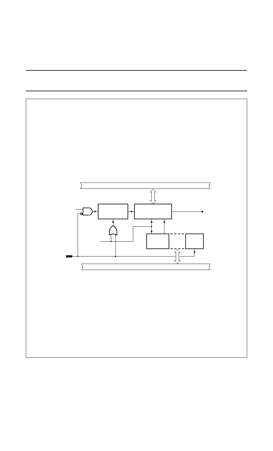
1999 Aug 19
121
Philips Semiconductors
Objective Specification
Single-chip 8-bit microcontroller with CAN controller
P8xC591
Fig.46 Functional diagram of T3 Watchdog Timer.
(1) See Fig.8.
handbook, full pagewidth
MHI047
INTERNAL BUS
1/6 fclk
write T3
PRESCALER
11-BIT
TIMER T3 (8-BIT)
LOAD
CLEAR
to reset circuitry
(1)
LOADEN
AUXR1.4
WDE
LOADEN
PCON.4
PCON.1
CLEAR
WLE
PD
INTERNAL BUS

1999 Aug 19
122
Philips Semiconductors
Objective Specification
Single-chip 8-bit microcontroller with CAN controller
P8xC591
18 PULSE WIDTH MODULATED OUTPUTS
The P8xC591 contains two Pulse Width Modulated (PWM)
output channels (see Fig.47). These channels generate
pulses of programmable length and interval. The repetition
frequency is defined by an 8-bit prescaler PWMP, which
supplies the clock for the counter. The prescaler and
counter are common to both PWM channels. The 8-bit
counter counts modulo 255, i.e., from 0 to 254 inclusive.
The value of the 8-bit counter is compared to the contents
of two registers: PWM0 and PWM1.
Provided the contents of either of these registers is greater
than the counter value, the corresponding PWM0 or
PWM1 output is set LOW. If the contents of these registers
are equal to, or less than the counter value, the output will
be HIGH. The pulse-width-ratio is therefore defined by the
contents of the registers PWM0 and PWM1. The
pulse-width-ratio is in the range of
0
/
255
to
255
/
255
and may
be programmed in increments of
1
/
255
.
Buffered PWM outputs may be used to drive DC motors.
The rotation speed of the motor would be proportional to
the contents of PWMn. The PWM outputs may also be
configured as a dual DAC.
In this application, the PWM outputs must be integrated
using conventional operational amplifier circuitry. If the
resulting output voltages have to be accurate, external
buffers with their own analog supply should be used to
buffer the PWM outputs before they are integrated.
The repetition frequency f
PWM
, at the PWMn outputs is
given by:
This gives a repetition frequency range of 246 Hz to
62.8 kHz (at f
CLK
= 16 MHz). By loading the PWM
registers with either 00H or FFH, the PWM channels will
output a constant HIGH or LOW level, respectively. Since
the 8-bit counter counts modulo 255, it can never actually
reach the value of the PWM registers when they are
loaded with FFH.
When a compare register (PWM0 or PWM1) is loaded with
a new value, the associated output is updated
immediately. It does not have to wait until the end of the
current counter period. Both PWMn output pins are driven
by push-pull drivers. These pins are not used for any other
purpose.
f
PWM
f
CLK
PWMP
1
+
(
)
255
◊
------------------------------------------------------
=
Fig.47 Functional diagram of Pulse Width Modulated outputs.
handbook, full pagewidth
MHI048
fCLK
PWMP
PWM1
PRESCALER
8-BIT COUNTER
PWM0
INTERNAL BUS
8-BIT COMPARATOR
8-BIT COMPARATOR
OUTPUT
BUFFER
PWM1
OUTPUT
BUFFER
PWM0

1999 Aug 19
123
Philips Semiconductors
Objective Specification
Single-chip 8-bit microcontroller with CAN controller
P8xC591
18.1
Prescaler Frequency Control Register (PWMP)
Reading PWMP gives the current reload value. The actual count of the prescaler cannot be read.
Table 82 Prescaler Frequency Control Register (address FEH), Reset Value = 00H
Table 83 Description of PWMP bits
18.2
Pulse Width Register 0 (PWM0)
Table 84 Pulse width register (address FCH), Reset Value = 00H
Table 85 Description of PWM0 bits
18.3
Pulse Width Register 1 (PWM1)
Table 86 Pulse width register (address FDH)
Table 87 Description of PWM1 bits
7
6
5
4
3
2
1
0
PWMP.7
PWMP.6
PWMP.5
PWMP.4
PWMP.3
PWMP.2
PWMP.1
PWMP.0
BIT
SYMBOL
DESCRIPTION
7 to 0
PWMP.7 to PWMP.0
Prescaler division factor. The Prescaler division factor = (PWMP) + 1.
7
6
5
4
3
2
1
0
PWM0.7
PWM0.6
PWM0.5
PWM0.4
PWM0.3
PWM0.2
PWM0.1
PWM0.0
BIT
SYMBOL
DESCRIPTION
7 to 0
PWM0.7 to PWM0.0
Pulse width ratio.
7
6
5
4
3
2
1
0
PWM1.7
PWM1.6
PWM1.5
PWM1.4
PWM1.3
PWM1.2
PWM1.1
PWM1.0
BIT
SYMBOL
DESCRIPTION
7 to 0
PWM1.7 to PWM1.0
Pulse width ratio.
LOW/HIGH ratio of PWM0 signals
PWM0
(
)
255
PWM0
(
)
≠
------------------------------------------
=
LOW/HIGH ratio of PWM1 signals
PWM1
(
)
255
PWM1
(
)
≠
------------------------------------------
=

1999 Aug 19
124
Philips Semiconductors
Objective Specification
Single-chip 8-bit microcontroller with CAN controller
P8xC591
19 PORT 1 OPERATION
Port 1 may be used to input up to 6 analog signals ADC.
Unused ADC inputs may be used to input digital inputs.
These inputs have an inherent hysteresis to prevent the
input logic from drawing excessive current from the power
lines when driven by analog signals. Channel to channel
crosstalk (Ct) should be taken into consideration when
both analog and digital signals are simultaneously input to
Port 3 (see Chapter 24 "DC Characteristics").
20 ANALOG-TO-DIGITAL CONVERTER (ADC)
20.1
ADC features
∑
10-bit resolution
∑
6 multiplexed analog inputs
∑
Start of a conversion by software or with an external
signal
∑
Conversion time for one analog-to-digital conversion:
18.75
µ
s @ 16 MHz
∑
Differential non-linearity (DL
e
): ±
1 LSB
∑
Integral non-linearity (IL
e
):
±
2 LSB
∑
Offset error (OS
e
): ±
2 LSB
∑
Gain error (G
e
):
±
4%
∑
Absolute voltage error (A
e
): 3 LSB
∑
Channel-to-channel matching (M
ctc
):
±
1 LSB
∑
Crosstalk between analog inputs (C
t
): < 60 dB at
100 kHz
∑
Monotonic and no missing codes
∑
Separated analog (V
SSA
) and digital (V
DD
, V
SS
) supply
voltages
∑
Reference voltage special pin: V
ref(p)(A)
.
For information on the ADC characteristics, refer to
Chapter 24.
20.2
ADC functional description
The analog input circuitry consists of an 6-input analog
multiplexer and a 10-bit, straight binary, successive
approximation ADC. The A/D can also be operated in 8-bit
mode with faster conversion times by setting bit ADC8
(AUXR1.7). The 8-bit result will be contained in the ADCH
register. The analog reference voltage and analog power
supplies are connected via separate input pins. For 10-bit
accuracy, the conversion takes 50 machine cycles, i.e.,
18.75
µ
s at an oscillator frequency of 16 MHz. For the 8-bit
mode, the conversion takes 24 machine cycles. Input
voltage swing is from 0 V to +5 V. Because the internal
DAC employs a ratiometric potentiometer, there are no
discontinouties in the converter characteristic. Figure 48
shows a functional diagram of the analog input circuitry.
The ADC has the option of either being powered off in Idle
mode for reduced power consumption or being active in
the Idle mode for reducing internal noise during the
conversion. This option is selected by the AIDL bit of
AUXR1 register (AUXR1.6). With the AIDL bit set, the ADC
is active in the Idle mode, and with the AIDL bit cleared,
the ADC is powered off in Idle mode.

1999 Aug 19
125
Philips Semiconductors
Objective Specification
Single-chip 8-bit microcontroller with CAN controller
P8xC591
Fig.48 Functional diagram of Analog Input Circuitry.
handbook, full pagewidth
MHI050
INTERNAL BUS
ANALOG INPUT
MULTIPLEXER
ADC0
ADC1
ADC2
ADC3
ADC4
ADC5
ANALOG GROUND
ANALOG REF.
+
n.c.
n.c.
1
2
0
4
5
6
7
3
10-BIT A/D CONVERTER
1
2
0
4
5
6
7
ADCH
ADCON
3
20.3
10-Bit Analog-to-Digital Conversion
Figure 48 shows the elements of a successive
approximation (SA) ADC. The ADC contains a DAC which
converts of a successive approximation register to a
voltage (VDAC) which is compared to the analog input
voltage (V
IN
). The output of the comparator is fed to the
successive approximation control logic which controls the
successive approximation register. A conversion is
initiated by setting ADCS in ADCON register. ADCS can
bet set by software only.
The software start mode is selected when control bit
ADCON.5 (ADEX) = 0. A conversion is then started by
setting control bit ADCON.3 (ADCS). The software start
mode is selected when ADCON.5 = 1, and a conversion
may be started by setting ADCON.3.
When a conversion is initiated, the conversion starts at the
beginning of the machine cycle which follows the
instruction that sets ADCS. ADCS is actually implemented
with two flip-flops; a command flip-flop which is affected by
set operations, and a status flag which is accessed during
read operations.
The next two machine cycles are used to initiate the
converter. At the end of the first cycle, the ADCS status
flag is set and a value of "1" will be returned if the ADCS
flag is read while the conversion is progress. Sampling of
the analog input commences at the end of the second
cycle.
During the next eight machine cycles, the voltage at the
previously selected pin of port 1 is sampled, and this input
voltage should be stable in order to obtain a useful sample.
In any event, the input voltage slew rate must be less than
10 V/ms in order to prevent an undefined result.
The successive approximation control logic first sets the
most significant bit and clears all other bits in the
successive approximation register (10 0000 0000B). The
output of the DAC (50% full scale) is compared to the input
voltage V
IN
. If the input voltage is greater than VDAC, then
the bit remains set; otherwise it is cleared.
The successive approximation control logic now sets the
next most significant bit (11 0000 0000B or
01 0000 0000B, depending on the previous result), and
VDAC is compared to V
IN
again. If the input voltage is
greater than VDAC, then the bit being tested remains set;

1999 Aug 19
126
Philips Semiconductors
Objective Specification
Single-chip 8-bit microcontroller with CAN controller
P8xC591
otherwise the bit being tested is cleared. This process is
repeated until all ten bits have been tested, at which stage
the result of the conversion is held in the successive
approximation register. Figure 48 shows a conversion flow
chart. The bit pointer identifies the bit under test. The
conversion takes four machine cycles per bit.
The end of the 10-bit conversion is flagged by control bit
ADCON.4 (ADCI). The upper 8 bits of the result are held in
Special Function Register ADCH, and the two remaining
bits are held in ADCON.7 (ADC.1) and ADCON.6 (ADC.0).
The user may ignore the two least significant bits in
ADCON and use the ADC as an 8-bit converter (8 upper
bits in ADCH). In any event, the total actual conversion
time is 50 machine cycles for the P8xC591. ADCI will be
set and the ADCS status flag will be reset 50 (or 24) cycles
after the command flip-flop (ADCS) is set.
Control bits ADCON.0, ADCON.1, and ADCON.2 are used
to control an analog multiplexer which selects one of six
analog channels (see Section 20.3.1). An ADC conversion
in progress is unaffected by a new software ADC start. The
result of a completed conversion remains unaffected
provided ADCI = logic 1; a new ADC conversion already in
progress is aborted when the Idle or Power-down mode is
entered. The result of a completed conversion (ADCI =
logic 1) remains unaffected when entering the Idle mode.
Fig.49 Successive Approximation ADC.
handbook, full pagewidth
MHI051
SUCCESSIVE
APPROXIMATION
REGISTER
DAC
SUCCESSIVE
APPROXIMATION
CONTROL LOGIC
START
STOP
Vin
VDAC
full scale
t/tau
VDAC
1/2
3/4
7/8
15/16
29/32
59/64
1
1
0
2
3
4
5
6
Vin
1999 Aug 19
127
Philips Semiconductors
Objective Specification
Single-chip 8-bit microcontroller with CAN controller
P8xC591
Fig.50 A/D Conversion Flowchart.
handbook, full pagewidth
MHI052
RESET SAR
SOC
[BIT POINTER] = MSB
CONVERSION TIME
TEST
COMPLETE
[BIT]N = 1
[BIT]N = 0
1
0
[BIT POINTER]
+
1
END
END
End of conversion
Start of conversion
EOC
TEST BIT
POINTER

1999 Aug 19
128
Philips Semiconductors
Objective Specification
Single-chip 8-bit microcontroller with CAN controller
P8xC591
20.3.1
ADC C
ONTROL
R
EGISTER
(ADCON)
Table 88 ADC Control Register (address C5H); Reset value = xx00 0000B
Table 89 Description of ADCON bits
Table 90 ADC status
Table 91 Selected analog channel
7
6
5
4
3
2
1
0
ADC.1
ADC.0
ADEX
ADCI
ADCS
AADR2
AADR1
AADR0
BIT
SYMBOL
DESCRIPTION
7
ADC.1
Bit 1 of ADC result.
6
ADC.0
Bit 0 of ADC result.
5
-
Reserved for future use.
4
ADCI
ADC interrupt flag. This flag is set when an A/D conversion result is ready to be read.
An interrupt is invoked if its is enabled. The flag may be cleared by the interrupt service
routine. While this flag is set, the ADC cannot start a new conversion. ADCI cannot be
set by software.
3
ADCS
ADC start and status. Setting this bit starts an A/D conversion. It is set by software.
The ADC logic ensures that this signal is HIGH while the ADC is busy. On completion of
the conversion. ADCS is reset immediately after the interrupt flag has been set. ADCS
cannot be reset by software. A new conversion may not be started while either ADCS or
ADCI is high (see Table 90).
If ADDCI is cleared by software while ADCS is set at the same time, a new A/D
conversion with the same channel number may be started.
But it is recommended to reset ADCI before ADCS is set.
2 to 0
AADR2 to
AADR0
Analogue input select: This binary coded address selects one of the six analogue port
bits of P1 to be input to the converter. It can only be changed when ADCI and ADCS are
both LOW.
ADCI
ADCS
ADC STATUS
0
0
ADC not busy; a conversion can be started
0
1
ADC busy; start of a new conversion is blocked
1
0
Conversion completed; start of a new conversion requires ADCI=0
1
1
Conversion completed; start of a new conversion requires ADCI=0
AADR2
AADR1
AADR0
SELECTED ANALOG CHANNEL
0
0
0
ADC0 (P1.2)
0
0
1
ADC1 (P1.3)
0
1
0
ADC2 (P1.4)
0
1
1
ADC3 (P1.5)
1
0
0
ADC4 (P1.6)
1
0
1
ADC5 (P1.7)

1999 Aug 19
129
Philips Semiconductors
Objective Specification
Single-chip 8-bit microcontroller with CAN controller
P8xC591
20.4
10-Bit ADC Resolution and Analog Supply
Figure 48 shows how the ADC is realized. The ADC has its
own analog ground (AV
SS
) and a positive analog reference
pin (V
ref+
) connected to each end of the DAC's
resistance-ladder. The ladder has 1023 equally spaced
taps, separated by a resistance of "R". The first tap is
located 0.5 x R above AV
SS
, and the last tap is located
1.5 x R below V
ref+
. This gives a total ladder resistance of
1024 x R. This structure ensures that the DAC is
monotonic and results in a symmetrical quantization error
is shown in Figure 48.
For input voltages between 0 V and + 1/2 LSB, the 10-bit
result of an A/D conversion will be 00 0000 0000B =
0000H. For input voltages between (V
ref+
) - 3/2 LSB and
V
ref+
, the result of a conversion will be 11 1111 1111B =
3FFFH. AV
ref+
may be between V
DD
+0.2 V and AV
SS
-
0.2 V. AV
ref+
should be positive 0 V and AV
ref+
. If the
analog input voltage range is from 2 V to 4 V, the 10-bit
resolution can be obtained over this range if AV
ref+
= 4 V.
The result can always can always be calculated from the
following formula:
Result = 1024
V
IN
AV
ref+
----------------
◊
20.5
Power Reduction Modes
The P8xC591 has two reduced power modes of operation:
the Idle mode and the Power-down mode. These modes
are entered by setting bits in the PCON Special Function
Register. When the P8xC591 enters the Idle mode, the
following functions are disabled:
CPU
(halted)
Timer T2
(halted and reset)
PWM0, PWM1
(reset; outputs are high)
ADC
(may be enabled for operation in Idle
mode by setting bit AIDC (AUXR1.6).
In Idle mode, the following functions remain active:
Timer 0
Timer 1
Timer T3
SIO0 SIO1
External interrupts
When the P8xC591 enters the Power-down mode, the
oscillator is stopped. The Power-down mode is entered by
setting the PD bit in the PCON register. The PD bit can
only be set if the `WDE' bit is 0.
Fig.51 ADC Realization.
Value 0000 0000 00
is output for voltages 0 V +
1
/
2
LSB
Value 1111 1111 11
is output for voltages (V
ref+
±
3
/
2
LSB) to V
ref+
handbook, full pagewidth
MHI053
R/2
AVref
+
R
R
R
R
R/2
AVSS
Vin
Vref
Total resistance
= 1023R
+
2
◊
R/
= 1024R
COMPARATOR
DECODER
START
LSB
MSB
SUCCESSIVE
APPROXIMATION
REGISTER
SUCCESSIVE
APPROXIMATION
CONTROL LOGIC
READY
1021
1022
1023
1
0
2
3

1999 Aug 19
130
Philips Semiconductors
Objective Specification
Single-chip 8-bit microcontroller with CAN controller
P8xC591
Fig.52 A/D Input: Equivalent Circuit.
handbook, full pagewidth
MHI054
MULTIPLEXER
RmN
+
1
RmN
SmN
+
1
Cc
Cs
IN
+
1
IN
SmN
Rs
+
VANALOG
input
to comparator
Rm = 0.5 - 3 k
C
S
+ C
C
= 15 pF maximum
R
S
= Recommended < 9.6 k
for 1 LSB @ 12 MHz
Note:
Because the analog to digital converter has a sampled-data comparator, the input looks capacitive to a source. When a conversion is initiated, switch Sm
closes for 8 t
CY
(4
µ
s @ 12 MHz crystal frequency) during which time capacitance C
S
+ C
C
is changed. It should be noted that the sampling causes the
analog input to prevent a varying load to an analog source.
Fig.53 Effective Conversion Characteristic.
handbook, full pagewidth
MHI055
101
100
011
010
001
000
0
q
q = LSB = 5 mV
+
q/2
-
q/2
2q
3q
4q
5q
Vin
Vin
Vin
-
Vdigital
CODE
OUT
QUANTIZATION ERROR
SYMMETRICAL QUANTIZATION ERROR

1999 Aug 19
131
Philips Semiconductors
Objective Specification
Single-chip 8-bit microcontroller with CAN controller
P8xC591
21 INTERRUPTS
The 8xC591 has fifteen interrupt sources, each of which
can be assigned one of four priority levels. The five
interrupt sources common to the 80C51 are the external
interrupts (INT0 and INT1), the timer 0 and timer 1
interrupts (lT0 and IT1), and the serial I/O interrupt (RI or
TI). In the 8xC591, the standard serial interrupt is called
SIO0.
The seven Timer T2 interrupts are generated by flags
CTl0-CTI3, CMl0-CMl1, and by the logical OR of flags
T2OV and T2BO. Flags CTl0 to CTI3 are set by input
signals CT0l to CT3I. The inputs INT2 to INT5 can be
regarded as 4 additional external interrupts, if the capture
facility of Timer T2 is not used (details see Timer T2 in
Section 16.1.4.1).
Flags CMl0 to CMl1 are set when a match occurs between
Timer T2 and the compare registers CM0 and CM1. When
an 8-bit or 16-bit overflow occurs, flags T2BO and T2OV
are set, respectively. These eight flags are not cleared by
hardware and must be reset by software to avoid recurring
interrupts.
The ADC interrupt is generated by the ADCl flag in the
ADC control register (ADCON). This flag is set when an
ADC conversion result is ready to be read. ADCl is not
cleared by hardware and must be reset by software to
avoid recurring interrupts. The SIO1 (I
2
C) interrupt is
generated by the SI flag in the SI01 control register
(S1CON). This flag is set when S1STA is loaded with a
valid status code.
The ADCl flag may be reset by software. It cannot be set
by software. All other flags that generate interrupts may be
set or cleared by software, and the effect is the same as
setting or resetting the flags by hardware. Thus, interrupts
may be generated by software and pending interrupts can
be cancelled by software.
A CAN interrupt is generated (vector address 006BH)
when one or more bits of CANCON register are set (refer
to CAN Section 12.5.5 Interrupt Register (IR) for details).
21.1
Interrupt Enable Registers
Each interrupt source can be individually enabled or
disabled by setting or clearing a bit in the interrupt enable
Special Function Registers lENO and lEN1. All interrupt
sources can also be globally enabled or disabled by setting
or clearing bit EA in lENO. The interrupt enable registers
are described in Section 21.2.1 and 21.2.2).
There are 3 SFRs associated with each of the four-level
interrupts. They are the lENx, lPx, and lPxH (see
Section 21.2.3 to 21.2.6). The lPxH (Interrupt Priority
High) register makes the four-level interrupt structure
possible.
The function of the lPxH SFR is simple and when
combined with the lPx SFR determines the priority of each
interrupt. The priority of each interrupt is determined as
shown in the following table:
Table 92
The priority scheme for servicing the interrupts is the same
as that for the 80C51, except there are four interrupt levels
rather than two as on the 80C51. An interrupt will be
serviced as long as an interrupt of equal or higher priority
is not already being serviced. If an interrupt of equal or
higher level priority is being serviced, the new interrupt will
wait until it is finished before being serviced. If a lower
priority level interrupt is being serviced, it will be stopped
and the new interrupt serviced. When the new interrupt is
finished, the lower priority level interrupt that was stopped
will be completed.
PRIORITY BITS
INTERRUPT PRIORITY LEVEL
IPxH.x
IPx.x
0
0
Level 0 (lowest priority)
0
1
Level 1
1
0
Level 2
1
1
Level 3 (highest priority)

1999 Aug 19
132
Philips Semiconductors
Objective Specification
Single-chip 8-bit microcontroller with CAN controller
P8xC591
21.2
Interrupt Enable and Priority Registers
21.2.1
I
NTERRUPT
E
NABLE
R
EGISTER
0 (IEN0)
Logic 0 = interrupt disabled; logic 1 = interrupt enabled.
Table 93 Interrupt Enable Register 0 (address A8H)
Table 94 Description of IEN0 bits
21.2.2
I
NTERRUPT
E
NABLE
R
EGISTER
1 (IEN1)
Logic 0 = interrupt disabled; logic 1 = interrupt enabled.
Table 95 Interrupt Enable Register 1 (address E8H)
Table 96 Description of IEN1 bits
7
6
5
4
3
2
1
0
EA
EAD
ES1
ES0
ET1
EX1
ET0
EX0
BIT
SYMBOL
DESCRIPTION
7
EA
Global enable/disable control. If bit EA is:
LOW, then no interrupt is enabled.
HIGH, then any individually enabled interrupt will be accepted.
6
EAD
Enable ADC interrupt.
5
ES1
Enable SIO1 (I
2
C) interrupt.
4
ES0
Enable SIO0 (UART) interrupt.
3
ET1
Enable Timer 1 interrupt.
2
EX1
Enable External 1 interrupt / Seconds interrupt.
1
ET0
Enable Timer 0 interrupt.
0
EX0
Enable External 0 interrupt.
7
6
5
4
3
2
1
0
ET2
ECAN
ECM1
ECM0
ECT3
ECT2
ECT1
ECT0
BIT
SYMBOL
DESCRIPTION
7
ET2
Enable T2 overflow interrupt(s).
6
ECAN
Enable CAN interrupt.
5
ECM1
Enable T2 comparator 1 interrupt.
4
ECM0
Enable T2 comparator 0 interrupt.
3
ECT3
Enable T2 capture register 3 interrupt.
2
ECT1
Enable T2 capture register 2 interrupt.
1
ECT1
Enable T2 capture register 1 interrupt.
0
ECT0
Enable T2 capture register 0 interrupt.

1999 Aug 19
133
Philips Semiconductors
Objective Specification
Single-chip 8-bit microcontroller with CAN controller
P8xC591
21.2.3
I
NTERRUPT
P
RIORITY
R
EGISTER
0 (IP0)
Logic 0 = low priority; logic 1 = high priority.
Table 97 Interrupt Priority Register 0 (address B8H)
Table 98 Description of IP0 bits
21.2.4
I
NTERRUPT
P
RIORITY
H
IGH
R
EGISTER
0 (IP0H)
Logic 0 = low priority; logic 1 = high priority.
Table 99 Interrupt Priority High Register 0 (address B7H)
Table 100Description of IP0H bits
7
6
5
4
3
2
1
0
-
PAD
PS1
PS0
PT1
PX1
PT0
PX0
BIT
SYMBOL
DESCRIPTION
7
-
Reserved for future use.
6
PAD
ADC interrupt priority level.
5
PS1
SIO1 (I
2
C) interrupt priority level.
4
PS0
SIO0 (UART) interrupt priority level.
3
PT1
Timer 1 interrupt priority level.
2
PX1
External interrupt 1/Seconds priority level.
1
PT0
Timer 0 interrupt priority level.
0
PX0
External interrupt 0 priority level.
7
6
5
4
3
2
1
0
-
PADH
PS1H
PS0H
PT1H
PX1H
PT0H
PX0H
BIT
SYMBOL
DESCRIPTION
7
-
Reserved for future use.
6
PADH
ADC interrupt priority level.
5
PS1H
SIO1 (I
2
C) interrupt priority level.
4
PS0H
SIO0 (UART) interrupt priority level.
3
PT1H
Timer 1 interrupt priority level.
2
PX1H
External interrupt 1/Seconds priority level.
1
PT0H
Timer 0 interrupt priority level.
0
PX0H
External interrupt 0 priority level.

1999 Aug 19
134
Philips Semiconductors
Objective Specification
Single-chip 8-bit microcontroller with CAN controller
P8xC591
21.2.5
I
NTERRUPT
P
RIORITY
R
EGISTER
1 (IP1)
Logic 0 = low priority; logic 1 = high priority.
Table 101Interrupt Priority Register 1 (address F8H)
Table 102Description of IP1 bits
21.2.6
I
NTERRUPT
P
RIORITY
R
EGISTER
H
IGH
1 (IP1H)
Logic 0 = low priority; logic 1 = high priority.
Table 103Interrupt Priority Register High 1 (address F7H)
Table 104Description of IP1H bits
7
6
5
4
3
2
1
0
PT2
PCAN
PCM1
PCM0
PCT3
PCT2
PCT1
PCT0
BIT
SYMBOL
DESCRIPTION
7
PT2
T2 overflow interrupt(s) priority level.
6
PCAN
CAN interrupt priority level.
5
PCM1
T2 comparator 1 interrupt priority level.
4
PCM0
T2 comparator 0 interrupt priority level.
3
PCT3
T2 capture register 3 interrupt priority level.
2
PCT2
T2 capture register 2 interrupt priority level.
1
PCT1
T2 capture register 1 interrupt priority level.
0
PCT0
T2 capture register 0 interrupt priority level.
7
6
5
4
3
2
1
0
PT2
PCANH
PCM1H
PCM0H
PCT3H
PCT2H
PCT1H
PCT0H
BIT
SYMBOL
DESCRIPTION
7
PT2
T2 overflow interrupt(s) priority level.
6
PCANH
CAN interrupt priority level high.
5
PCM1H
T2 comparator 1 interrupt priority level.
4
PCM0H
T2 comparator 0 interrupt priority level.
3
PCT3H
T2 capture register 3 interrupt priority level.
2
PCT2H
T2 capture register 2 interrupt priority level.
1
PCT1H
T2 capture register 1 interrupt priority level.
0
PCT0H
T2 capture register 0 interrupt priority level.

1999 Aug 19
135
Philips Semiconductors
Objective Specification
Single-chip 8-bit microcontroller with CAN controller
P8xC591
21.3
Interrupt priority
Table 105 Interrupt priority structure
SOURCE
SYMBOL
PRIORITY
WITHIN LEVEL
External interrupt 0
X0
(highest)
SIO1 (I
2
C)
S1
ADC completion
ADC
Timer 0 overflow
T0
T2 capture 0
CT0
T2 compare 0
CM0
External interrupt 1
X1
T2 capture 1
CT1
T2 compare 1
CM1
Timer 1 overflow
T1
T2 capture 2
CT2
CAN
CAN
Serial I/O 0 (UART)
S0
T2 compare 3
CT3
Timer T2 overflow
T2
(lowest)
21.4
Interrupt Vectors
The vector indicates the Program Memory location where
the appropriate interrupt service routine starts (see
Table 106).
Table 106 Interrupt vector addresses
SOURCE
SYMBOL
VECTOR
External interrupt 0
X0
0003H
Timer 0 overflow
T0
000BH
External interrupt 1
X1
0013H
Timer 1 overflow
T1
001BH
Serial I/O 0 (UART)
S0
0023H
SIO1 (I
2
C)
S1
002BH
T2 capture 0
CT0
0033H
T2 capture 1
CT1
003BH
T2 capture 2
CT2
0043H
T2 capture 3
CT3
004BH
ADC completion
ADC
0053H
T2 compare 0
CM0
005BH
T2 compare 1
CM1
0063H
CAN interrupt
CAN
006BH
T2 overflow
T2
0073H

1999 Aug 19
136
Philips Semiconductors
Objective Specification
Single-chip 8-bit microcontroller with CAN controller
P8xC591
22 INSTRUCTION SET
For the description of the Data Addressing Modes and Hexadecimal opcode cross-reference see Table 111.
Table 107 Instruction set description: Arithmetic operations
MNEMONIC
DESCRIPTION
BYTES
CYCLES
OPCODE
(HEX)
Arithmetic operations
ADD
A,Rr
Add register to A
1
1
2*
ADD
A,direct
Add direct byte to A
2
1
25
ADD
A,@Ri
Add indirect RAM to A
1
1
26, 27
ADD
A,#data
Add immediate data to A
2
1
24
ADDC
A,Rr
Add register to A with carry flag
1
1
3*
ADDC
A,direct
Add direct byte to A with carry flag
2
1
35
ADDC
A,@Ri
Add indirect RAM to A with carry flag
1
1
36, 37
ADDC
A,#data
Add immediate data to A with carry flag
2
1
34
SUBB
A,Rr
Subtract register from A with borrow
1
1
9*
SUBB
A,direct
Subtract direct byte from A with borrow
2
1
95
SUBB
A,@Ri
Subtract indirect RAM from A with borrow
1
1
96, 97
SUBB
A,#data
Subtract immediate data from A with borrow
2
1
94
INC
A
Increment A
1
1
04
INC
Rr
Increment register
1
1
0*
INC
direct
Increment direct byte
2
1
05
INC
@Ri
Increment indirect RAM
1
1
06, 07
DEC
A
Decrement A
1
1
14
DEC
Rr
Decrement register
1
1
1*
DEC
direct
Decrement direct byte
2
1
15
DEC
@Ri
Decrement indirect RAM
1
1
16, 17
INC
DPTR
Increment data pointer
1
2
A3
MUL
AB
Multiply A and B
1
4
A4
DIV
AB
Divide A by B
1
4
84
DA
A
Decimal adjust A
1
1
D4

1999 Aug 19
137
Philips Semiconductors
Objective Specification
Single-chip 8-bit microcontroller with CAN controller
P8xC591
Table 108 Instruction set description: Logic operations
MNEMONIC
DESCRIPTION
BYTES
CYCLES
OPCODE
(HEX)
Logic operations
ANL
A,Rr
AND register to A
1
1
5*
ANL
A,direct
AND direct byte to A
2
1
55
ANL
A,@Ri
AND indirect RAM to A
1
1
56, 57
ANL
A,#data
AND immediate data to A
2
1
54
ANL
direct,A
AND A to direct byte
2
1
52
ANL
direct,#data
AND immediate data to direct byte
3
2
53
ORL
A,Rr
OR register to A
1
1
4*
ORL
A,direct
OR direct byte to A
2
1
45
ORL
A,@Ri
OR indirect RAM to A
1
1
46, 47
ORL
A,#data
OR immediate data to A
2
1
44
ORL
direct,A
OR A to direct byte
2
1
42
ORL
direct,#data
OR immediate data to direct byte
3
2
43
XRL
A,Rr
Exclusive-OR register to A
1
1
6*
XRL
A,direct
Exclusive-OR direct byte to A
2
1
65
XRL
A,@Ri
Exclusive-OR indirect RAM to A
1
1
66, 67
XRL
A,#data
Exclusive-OR immediate data to A
2
1
64
XRL
direct,A
Exclusive-OR A to direct byte
2
1
62
XRL
direct,#data
Exclusive-OR immediate data to direct byte
3
2
63
CLR
A
Clear A
1
1
E4
CPL
A
Complement A
1
1
F4
RL
A
Rotate A left
1
1
23
RLC
A
Rotate A left through the carry flag
1
1
33
RR
A
Rotate A right
1
1
03
RRC
A
Rotate A right through the carry flag
1
1
13
SWAP
A
Swap nibbles within A
1
1
C4

1999 Aug 19
138
Philips Semiconductors
Objective Specification
Single-chip 8-bit microcontroller with CAN controller
P8xC591
Table 109 Instruction set description: Data transfer
Note
1. MOV A,ACC is not permitted.
MNEMONIC
DESCRIPTION
BYTES
CYCLES
OPCODE
(HEX)
Data transfer
MOV
A,Rr
Move register to A
1
1
E*
MOV
A,direct (Note 1) Move direct byte to A
2
1
E5
MOV
A,@Ri
Move indirect RAM to A
1
1
E6, E7
MOV
A,#data
Move immediate data to A
2
1
74
MOV
Rr,A
Move A to register
1
1
F*
MOV
Rr,direct
Move direct byte to register
2
2
A*
MOV
Rr,#data
Move immediate data to register
2
1
7*
MOV
direct,A
Move A to direct byte
2
1
F5
MOV
direct,Rr
Move register to direct byte
2
2
8*
MOV
direct,direct
Move direct byte to direct
3
2
85
MOV
direct,@Ri
Move indirect RAM to direct byte
2
2
86, 87
MOV
direct,#data
Move immediate data to direct byte
3
2
75
MOV
@Ri,A
Move A to indirect RAM
1
1
F6, F7
MOV
@Ri,direct
Move direct byte to indirect RAM
2
2
A6, A7
MOV
@Ri,#data
Move immediate data to indirect RAM
2
1
76, 77
MOV
DPTR,#data 16
Load data pointer with a 16-bit constant
3
2
90
MOVC
A,@A+DPTR
Move code byte relative to DPTR to A
1
2
93
MOVC
A,@A+PC
Move code byte relative to PC to A
1
2
83
MOVX
A,@Ri
Move external RAM (8-bit address) to A
1
2
E2, E3
MOVX
A,@DPTR
Move external RAM (16-bit address) to A
1
2
E0
MOVX
@Ri,A
Move A to external RAM (8-bit address)
1
2
F2, F3
MOVX
@DPTR,A
Move A to external RAM (16-bit address)
1
2
F0
PUSH
direct
Push direct byte onto stack
2
2
C0
POP
direct
Pop direct byte from stack
2
2
D0
XCH
A,Rr
Exchange register with A
1
1
C*
XCH
A,direct
Exchange direct byte with A
2
1
C5
XCH
A,@Ri
Exchange indirect RAM with A
1
1
C6, C7
XCHD
A,@Ri
Exchange LOW-order digit indirect RAM with A
1
1
D6, D7

1999 Aug 19
139
Philips Semiconductors
Objective Specification
Single-chip 8-bit microcontroller with CAN controller
P8xC591
Table 110 Instruction set description: Boolean variable manipulation, Program and machine control
MNEMONIC
DESCRIPTION
BYTES
CYCLES
OPCODE
(HEX)
Boolean variable manipulation
CLR
C
Clear carry flag
1
1
C3
CLR
bit
Clear direct bit
2
1
C2
SETB
C
Set carry flag
1
1
D3
SETB
bit
Set direct bit
2
1
D2
CPL
C
Complement carry flag
1
1
B3
CPL
bit
Complement direct bit
2
1
B2
ANL
C,bit
AND direct bit to carry flag
2
2
82
ANL
C,/bit
AND complement of direct bit to carry flag
2
2
B0
ORL
C,bit
OR direct bit to carry flag
2
2
72
ORL
C,/bit
OR complement of direct bit to carry flag
2
2
A0
MOV
C,bit
Move direct bit to carry flag
2
1
A2
MOV
bit,C
Move carry flag to direct bit
2
2
92
Program and machine control
ACALL
addr11
Absolute subroutine call
2
2
∑
1
LCALL
addr16
Long subroutine call
3
2
12
RET
Return from subroutine
1
2
22
RETI
Return from interrupt
1
2
32
AJMP
addr11
Absolute jump
2
2
1
LJMP
addr16
Long jump
3
2
02
SJMP
rel
Short jump (relative address)
2
2
80
JMP
@A+DPTR
Jump indirect relative to the DPTR
1
2
73
JZ
rel
Jump if A is zero
2
2
60
JNZ
rel
Jump if A is not zero
2
2
70
JC
rel
Jump if carry flag is set
2
2
40
JNC
rel
Jump if carry flag is not set
2
2
50
JB
bit,rel
Jump if direct bit is set
3
2
20
JNB
bit,rel
Jump if direct bit is not set
3
2
30
JBC
bit,rel
Jump if direct bit is set and clear bit
3
2
10
CJNE
A,direct,rel
Compare direct to A and jump if not equal
3
2
B5
CJNE
A,#data,rel
Compare immediate to A and jump if not equal
3
2
B4
CJNE
Rr,#data,rel
Compare immediate to register and jump if not equal
3
2
B*
CJNE
@Ri,#data,rel Compare immediate to indirect and jump if not equal
3
2
B6, B7
DJNZ
Rr,rel
Decrement register and jump if not zero
2
2
D*
DJNZ
direct,rel
Decrement direct and jump if not zero
3
2
D5
NOP
No operation
1
1
00

1999 Aug 19
140
Philips Semiconductors
Objective Specification
Single-chip 8-bit microcontroller with CAN controller
P8xC591
Table 111 Description of the mnemonics in the Instruction set
MNEMONIC
DESCRIPTION
Data addressing modes
Rr
Working register R0-R7.
direct
128 internal RAM locations and any special function register (SFR).
@Ri
Indirect internal RAM location addressed by register R0 or R1 of the actual register bank.
#data
8-bit constant included in instruction.
#data 16
16-bit constant included as bytes 2 and 3 of instruction.
bit
Direct addressed bit in internal RAM or SFR.
addr16
16-bit destination address. Used by LCALL and LJMP.
The branch will be anywhere within the 64 kbytes Program Memory address space.
addr11
11-bit destination address. Used by ACALL and AJMP. The branch will be within the same 2 kbytes
page of Program Memory as the first byte of the following instruction.
rel
Signed (two's complement) 8-bit offset byte. Used by SJMP and all conditional jumps.
Range is
-
128 to +127 bytes relative to first byte of the following instruction.
Hexadecimal opcode cross-reference
*
8, 9, A, B, C, D, E, F.
∑
1, 3, 5, 7, 9, B, D, F.
0, 2, 4, 6, 8, A, C, E.
22.1
Addressing Modes
Most instructions have a `destination, source' field that
specifies the data type, addressing modes and operands
involved. For all these instructions, except for MOVs, the
destination operand is also the source operand
(e.g. ADD A,R7).
There are five kinds of addressing modes:
∑
Register Addressing
≠ R0 - R7 (4 banks)
≠ A,B,C (bit), AB (2 bytes), DPTR (double byte)
∑
Direct Addressing
≠ lower 128 bytes of internal Main RAM (including the
4 R0-R7 register banks)
≠ Special Function Registers
≠ 128 bits in a subset of the internal Main RAM
≠ 128 bits in a subset of the Special Function Registers
∑
Register-Indirect Addressing
≠ internal Main RAM (@R0, @R1, @SP [PUSH/POP])
≠ internal Auxiliary RAM (@R0, @R1, @DPTR)
≠ external Data Memory (@R0, @R1, @DPTR)
∑
Immediate Addressing
≠ Program Memory (in-code 8 bit or 16 bit constant)
∑
Base-Register-plus-Index-Register-Indirect Addressing
≠ Program Memory look-up table
(@DPTR+A, @PC+A)
The first three addressing modes are usable for
destination operands.

1999 Aug 19
141
Philips Semiconductors
Objective Specification
Single-chip 8-bit microcontroller with CAN controller
P8xC591
23 LIMITING VALUES
In accordance with the Absolute Maximum Rating System (IEC 134); Note 1
Notes
1. The following applies to the Absolute Maximum Ratings:
a) Stresses above those listed under Absolute Maximum Ratings may cause permanent damage to the device. This
is a stress rating only and functional operation of the device at these or any conditions other than those described
in the Chapters 24 and 25 of this specification is not implied.
b) This product includes circuitry specifically designed for the protection of its internal devices from the damaging
effect of excessive static charge. However, its suggested that conventional precautions be taken to avoid
applying greater than the rated maxima.
c) Parameters are valid over operating temperature range unless otherwise specified. All voltages are with respect
to V
SS
unless otherwise noted.
2. This value is based on the maximum allowable die temperature and the thermal resistance of the package, not on
device power consumption.
SYMBOL
PARAMETER
MIN.
MAX.
UNIT
V
DD
Voltage on V
DD
to V
SS
and SCL, SDA to V
SS
-
0.5
+6.5
V
V
I
Input voltage on any other pin to V
SS
-
0.5
V
DD
+ 0.5
V
I
I
, I
O
Input/output current on any I/O pin
-
5
mA
P
tot
Total power dissipation (Note 2)
-
1.0
W
T
stg
Storage temperature range
-
65
+150
∞
C
T
amb
Operating ambient temperature range:
P8xC591SFx
-
40
+85
∞
C
V
PP
Voltage on EA/V
PP
to V
SS
-
0.5
+13
V

1999 Aug 19
142
Philips Semiconductors
Objective Specification
Single-chip 8-bit microcontroller with CAN controller
P8xC591
24 DC CHARACTERISTICS (VALUES IN THIS TABLE NOT CONFIRMED)
V
DD
= 5 V
±
10%; V
SS
= 0 V; all voltages with respect to V
SS
unless otherwise specified;
T
amb
=
-
40 to +85
∞
C for the P8xC591SFx; V
DD
= 5 V
±
10%; V
SS
= 0 V; AV
SS
= 0 V.
SYMBOL
PARAMETER
CONDITIONS
MIN.
MAX.
UNIT
Supply
I
DD
operating supply current
t
CLK
= 16 MHz;
see Notes 2 and 3
45
mA
I
ID
supply current Idle mode
t
CLK
= 16 MHz
see Notes 2 and 4
-
25
mA
I
PD
supply current Power-down mode
2 V < V
PD
< V
DD
;
see Notes 2 and 5
100
µ
A
Inputs
V
IL
LOW level input voltage
(except P1.0, P1.1, P1.6, P1.7)
-0.5
0.2 V
DD
-
0.1
V
V
IL1
LOW level input voltage EA
-0.5
0.2 V
DD
-
0.3
V
V
IL2
LOW level input voltage P1.0 and P1.1
0.2 V
DD
V
V
IL3
LOW level input voltage P1.6 and P1.7
see Note 6
-
0.5
0.3 V
DD
V
V
IH
HIGH level input voltage (except P1.0,
P1.1, P1.6, P1.7, XTAL1, RST)
0.2 V
DD
+ 0.9 V
DD
+ 0.5
V
V
IH1
HIGH level input voltage XTAL1, RST
0.7 V
DD
V
DD
+ 0.5
V
V
IH2
HIGH level input voltage P1.6 and P1.7
see Note 6
0.7 V
DD
6
V
V
IH3
HIGH level input voltage P1.0 and P1.1
0.8 V
DD
V
DD
V
I
IL
LOW level input current Ports 1, 2, and 3
in pseudo-bidirectional output mode
(except P1.6, P1.7)
V
IN
= 0.45 V
-
1
-
50
µ
A
I
TL
input current HIGH-to-LOW transition
Ports 1, 2, 3 in pseudo-bidirectional
output mode (except P1.6, P1.7)
-
650
µ
A
I
IL1
input leakage current, Ports 0, 2, 3 and
P1.0, P1.1 in high impedance
configurations
0.45 V
<
V
IN
<
V
DD
±
10
µ
A
I
IL2
input leakage current, Port 1
(except P1.0, P1.1)
0.45 V
<
V
IN
<
V
DD
1
µ
A

1999 Aug 19
143
Philips Semiconductors
Objective Specification
Single-chip 8-bit microcontroller with CAN controller
P8xC591
Outputs
V
OL
LOW level output voltage Ports 1, 2, 3
(except P1.0, P1.6, P1.7)
I
OL
= 1.6 mA;
see Note 8
0.4
V
V
OL1
LOW level output voltage Port 0, ALE,
PSEN, RST, PWM0, PWM1
I
OL
= 3.2; see Note 8
0.4
V
V
OL2
LOW level output voltage P1.6, P1.7
I
OL
= 3.0 mA;
see Note 8
-
0.4
V
V
OL3
LOW level output voltage P1.0 and P1.1
I
OL
= 8.0 mA
-
0.3 V
DD
V
V
OH
HIGH level output voltage Ports 1, 2, 3 in
pseudo-bidirectional output mode (except
P1.1, P1.6 and P1.7
I
OH
= -60
µ
A
2.4
V
V
OH1
HIGH level output voltage Port 0 and
Port 2 in external bus mode,
Port 2 in push-pull mode, ALE, PSEN,
PWM0, PWM1
I
OH
=
-
3.2 mA;
see Note 9
V
DD
-
0.7
V
V
OH2
HIGH level output voltage, P1.0 and P1.1 I
OH
=
-
1.6 mA
0.7 V
DD
V
V
OH3
HIGH level output voltage, Ports 1, 2, 3 in
push-pull output mode (except P1.0,
P1.1, P1.6, P1.7)
I
OH
=
-
1.6 mA
V
DD
-
0.7
V
R
RST
RST pull-up resistor
40
225
k
C
I/O
I/O pin capacitance
test frequency = 1 MHz;
T
amb
= 25
∞
C
-
15
pF
Analog inputs
AV
IN
analog input voltage
AV
SS
-
0.2
V
DD
+ 0.2
V
AV
ref+
reference voltage
-
V
DD
+ 0.2
V
R
REF
resistance between AV
ref+
and AV
SS
10
50
k
C
IA
analog input capacitance
-
15
pF
t
ADS
sampling time
-
5 tcy; Note 1
8 tcy
µ
s
µ
s
t
ADC
conversion time (including sampling time)
-
24 tcy; Note 1
50 tcy
µ
s
µ
s
DL
e
differential non-linearity
see Notes 10, 11, 12
-
±
1
LSB
IL
e8
integral non-linearity (8-bit mode)
-
±
1; Note 1
LSB
IL
e
integral non-linearity
see Notes 10, 13
-
±
2
LSB
OS
e8
offset error (8-bit mode)
-
±
1; Note 1
LSB
OS
e
offset error
see Notes 10, 15
-
±
2
LSB
G
e
gain error
-
±
0.4
%
A
e
absolute voltage error
see Notes 10, 16
-
±
3
LSB
M
ctc
channel-to-channel matching
-
±
1
LSB
C
t
crosstalk between analog inputs of Port 1 0 to 100 kHz;
see Notes 17, 18
-
-
60
dB
SYMBOL
PARAMETER
CONDITIONS
MIN.
MAX.
UNIT

1999 Aug 19
144
Philips Semiconductors
Objective Specification
Single-chip 8-bit microcontroller with CAN controller
P8xC591
Notes to the DC characteristics
1. 8-bit mode
2. See Figures 62 through 66 for I
DD
test conditions.
3. The operating supply current is measured with all output pins disconnected; XTAL1 driven with
t
r
= t
f
= 10 ns; V
IL
= V
SS
+ 0.5 V; V
IH
= V
DD
-
0.5 V; XTAL2 not connected; EA = RST = Port 0 = V
DD
.
4. The Idle mode supply current is measured with all output pins disconnected; XTAL1 driven with t
r
= t
f
= 10 ns;
V
IL
= V
SS
+ 0.5 V; V
IH
= V
DD
-
0.5 V; XTAL2 not connected; Port 0 = V
DD
; EA = RST = V
SS
.
5. The Power-down current is measured with all output pins disconnected; XTAL2 not connected;
Port 0 = V
DD
; EA = RST = XTAL1 = V
SS
.
6. The input threshold voltage of P1.6 and P1.7 (SIO1) meets the I
2
C specification, so an input voltage below 1.5 V will
be recognized as a logic 0 while an input voltage above 3.0 V will be recognized as a logic 1.
7. Pins of Port 1 (except P1.6, P1.7), 2 and 3 source a transition current when they are being externally driven from
HIGH to LOW. The transition current reaches its maximum value when V
IN
is approximately 2 V.
8. Capacitive loading on Ports 0 and 2 may cause spurious noise to be superimposed on the V
OL
of ALE and
Ports 1 and 3. The noise is due to external bus capacitance discharging into the Port 0 and Port 2 pins when these
pins make HIGH-to-LOW transitions during bus operations. In the worst cases (capacitive loading > 100pF), the
noise pulse on the ALE pin may exceed 0.8 V. In such cases, it may be desirable to qualify ALE with a Schmitt
Trigger, or use an address latch with a Schmitt Trigger STROBE input. I
OL
can exceed these conditions provided that
no single outputs sinks more than 5 mA and no more than two outputs exceed in the test conditions.
9. Capacitive loading on Ports 0 and 2 may cause the V
OH
on ALE and PSEN to momentarily fall below the 0.9 V
DD
specification when the address bits are stabilizing.
10. Conditions: AV
SS
= 0 V; V
DD
= 5.0 V. Measurement by continuous conversion of AV
IN
=
-
20 mV to 5.12 V in steps
of 0.5 mV, derivating parameters from collected conversion results of ADC. AV
REF+
(P8xC591) = 4.977 V, ADC is
monotonic with not missing codes.
11. The differential non-linearity (D
Le
) is the difference between the actual step width and the ideal step width (see
Fig.54).
12. The ADC is monotonic; there are no missing codes.
13. The integral non-linearity (I
Le
) is the peak difference between the centre of the steps of the actual and the ideal
transfer curve after appropriate adjustment of gain and offset error (see Fig.54).
14. The offset error (OS
e
) is the absolute difference between the straight line which fits the actual transfer curve (after
removing gain error), and a straight line which fits the ideal transfer curve (see Fig.54).
15. The gain error (G
e
) is the relative difference in percent between the straight line fitting the actual transfer curve (after
removing offset error), and the straight line which fits the ideal transfer curve. Gain error is constant at every point
on the transfer curve (see Fig.54).
16. The absolute voltage error (A
e
) is the maximum difference between the centre of the steps of the actual transfer curve
of the non-calibrated ADC and the ideal transfer curve.
17. This should be considered when both analog and digital signals are simultaneously input to Port 1.
18. The parameter is guaranteed by design and characterized, but is not production tested.
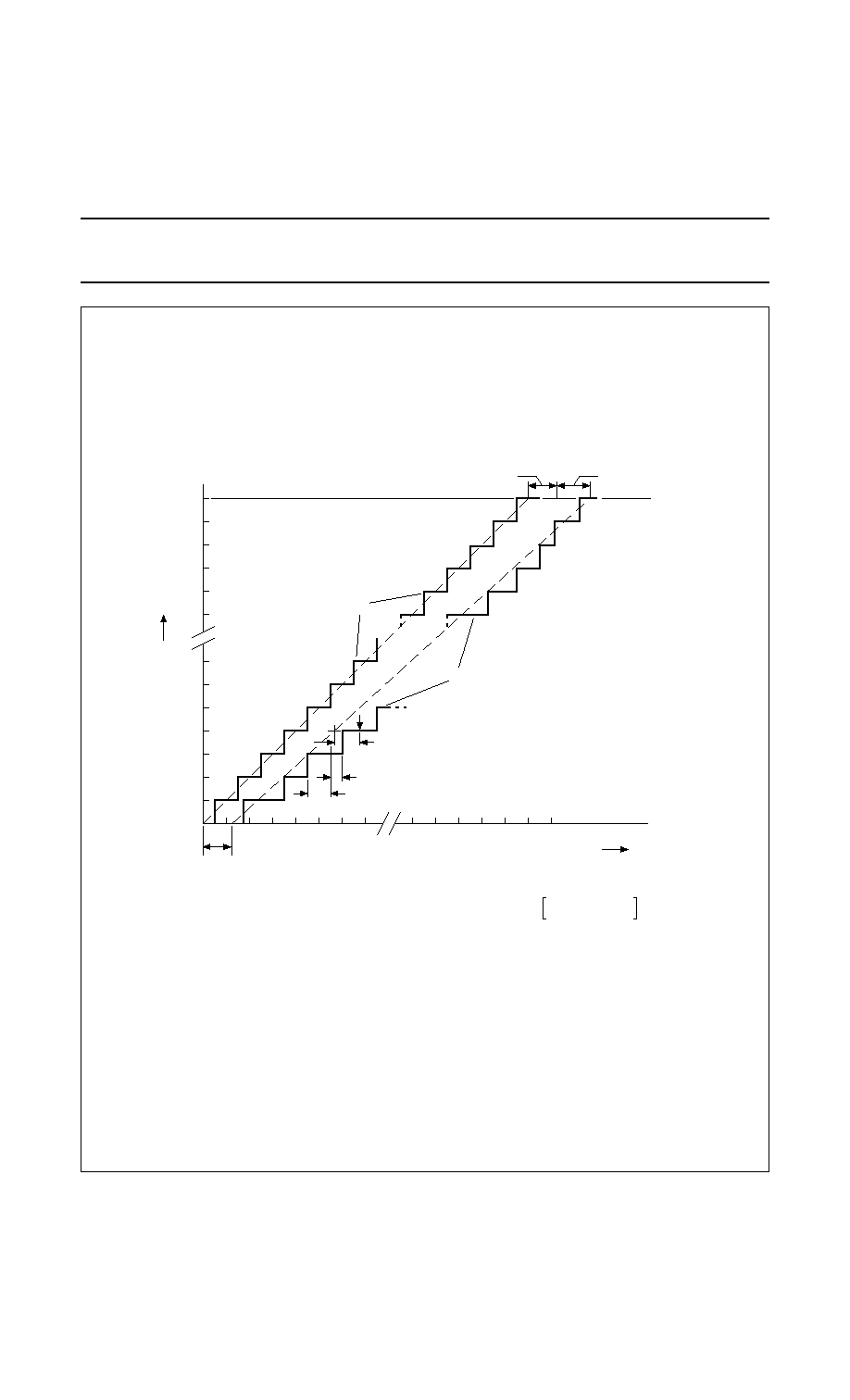
1999 Aug 19
145
Philips Semiconductors
Objective Specification
Single-chip 8-bit microcontroller with CAN controller
P8xC591
Fig.54 ADC conversion characteristic.
(1) Example of an actual transfer curve.
(2) The ideal transfer curve.
(3) Differential non-linearity (DL
e
).
(4) Integral non-linearity (IL
e
).
(5) Centre of a step of the actual transfer curve.
dbook, full pagewidth
MGD634
1
2
3
4
5
6
7
1018 1019 1020 1021 1022 1023 1024
0
1
2
3
4
5
6
7
1018
1019
1020
1021
1022
1023
Vin(A) (LSBideal)
code
out
offset error
OS
e
offset error OS e
gain error Ge
(2)
(3)
(4)
(5)
(1)
1 LSB (ideal)
1LSB
ideal
AV
REF+
1024
--------------------
=

1999 Aug 19
146
Philips Semiconductors
Objective Specification
Single-chip 8-bit microcontroller with CAN controller
P8xC591
25 AC CHARACTERISTICS
V
DD
= 5 V
±
10%; V
SS
= 0 V; T
amb
=
-
40
∞
C to +85
∞
C; C
L
= 100 pF for Port 0, ALE and PSEN; C
L
= 80 pF for all other
outputs unless otherwise specified.
SYMBOL
PARAMETER
16 MHz CLOCK
VARIABLE CLOCK
UNIT
MIN.
MAX.
MIN.
MAX.
External Program Memory; see Fig.55
1/f
CLK
System clock frequency; see Note 1
3.5
16
MHz
t
LHLL
ALE pulse width
22
-
0.5 t
CLK
-
25
-
ns
t
AVLL
address valid to ALE LOW
6
-
0.5 t
CLK
-
25
-
ns
t
LLAX
address hold after ALE LOW
6
-
0.5 t
CLK
-
25
-
ns
t
LLIV
ALE LOW to valid instruction in
-
60
-
2 t
CLK
-
65
ns
t
LLPL
ALE LOW to PSEN LOW
6
-
0.5 t
CLK
-
25
-
ns
t
PLPH
PSEN pulse width
48
-
1.5 t
CLK
-
45
-
ns
t
PLIV
PSEN LOW to valid instruction in
-
33
-
1.5 t
CLK
-
60
ns
t
PXIX
input instruction hold after PSEN
0
-
0
-
ns
t
PXIZ
input instruction float after PSEN
-
6
-
0.5 t
CLK
-
25
ns
t
AVIV
address to valid instruction in
-
76
-
2.5 t
CLK
-
80
ns
t
PLAZ
PSEN LOW to address float
-
10
-
10
ns
External Data Memory; see Fig.56 and Fig.57
t
RLRH
RD pulse width
87
-
3 t
CLK
-
100
-
ns
t
WLWH
WR pulse width
87
-
3 t
CLK
-
100
-
ns
t
RLDV
RD LOW to valid data in
-
66
-
2.5 t
CLK
-
90
ns
t
RHDX
data hold after RD
0
-
0
-
ns
t
RHDZ
data float after RD
-
34
-
2 t
CLK
-
28
ns
t
LLDV
ALE LOW to valid data in
-
100
-
4 t
CLK
-
150
ns
t
AVDV
address to valid data in
-
116
-
4.5 t
CLK
-
165 ns
t
LLWL
ALE LOW to RD or WR LOW
43
143
1.5 t
CLK
-
50
1.5 t
CLK
+ 50
ns
t
AVWL
address valid to RD or WR LOW
50
-
2 t
CLK
-
75
-
ns
t
QVWX
data valid to WR transition
0
-
0.5 t
CLK
-
30
-
ns
t
WHQX
data hold after WR
6
-
0.5 t
CLK
-
25
-
ns
t
QVWH
data valid time WR HIGH
88
-
3.5 t
CLK
-
130
-
ns
t
RLAZ
RD LOW to address float
-
0
-
0
ns
t
WHLH
RD or WR HIGH to ALE HIGH
6
56
0.5 t
CLK
-
25
0.5 t
CLK
+ 25
ns
External Clock; see Fig.65
t
CHCX
high time
t
CLK
◊
0.4 t
CLK
◊
0.6
t
CLK
◊
0.4
t
CLK
◊
0.6
ns
t
CLCX
low time
t
CLK
◊
0.4 t
CLK
◊
0.6
t
CLK
◊
0.4
t
CLK
◊
0.6
ns
t
CLCH
rise time
-
20
-
20
ns
t
CHCL
fall time
-
20
-
20
ns

1999 Aug 19
147
Philips Semiconductors
Objective Specification
Single-chip 8-bit microcontroller with CAN controller
P8xC591
Note
1. Parts a guaranteed to operate down to 0 Hz.
Table 112 I
2
C-bus interface timing
All values referred to V
IH(min)
and V
IL(max)
levels; see Fig.61.
Notes
1. At 100 kbit/s. At other bit rates this value is inversely proportional to the bit-rate of 100 kbit/s.
2. Determined by the external bus-line capacitance and the external bus-line pull-resistor, this must be < 1
µ
s.
3. Spikes on the SDA and SCL lines with a duration of less than 3 t
CLK
will be filtered out. Maximum capacitance on
bus-lines SDA and SCL = 400 pF.
4. t
CLK
= 1/f
CLK
= one oscillator clock period at pin XTAL1. For 62 ns < t
CLK
< 285 ns (8 MHz > f
CLK
> 3.5 MHz) the SI01
interface meets the I
2
C-bus specification for bit-rates up to 100 kbit/s.
5. These values are guaranteed but not 100% production tested.
UART Timing - Shift Register Mode; see Fig.59
t
XLXL
serial port clock cycle time
375
-
6 t
CLK
-
ns
t
QVXH
output data setup to clock rising edge
180
-
5 t
CLK
-
133
-
ns
t
XHQX
output data hold after clock rising edge
50
-
t
CLK
-
10
-
ns
t
XHDX
input data hold after clock rising edge
0
-
0
-
ns
t
XHDV
clock rising edge to input data valid
-
176
-
5 t
CLK
-
133
ns
SYMBOL
PARAMETER
I
2
C-BUS
INPUT
OUTPUT
t
HD;STA
START condition hold time
14 t
CLK
> 4.0
µ
s
(1)
t
LOW
LOW period of the SCL clock
16 t
CLK
> 4.7
µ
s
(1)
t
HIGH
HIGH period of the SCL clock
14 t
CLK
> 4.0
µ
s
(1)
t
RC
rise time of SCL signals
1
µ
s
-
(2)
t
FC
fall time of SCL signals
0.3
µ
s
< 3.0
µ
s
(3)
t
SU;DAT1
data set-up time
250 ns
> 20 t
CLK
-
t
RD
t
SU;DAT2
SDA set-up time (before repeated START condition)
250 ns
> 1
µ
s
(1)
t
SU;DAT3
SDA set-up time (before STOP condition)
250 ns
> 8 t
CLK
t
HD;DAT
data hold time
0 ns
> 8 t
CLK
-
t
FC
t
SU;STA
set-up time for a repeated START condition
14 t
CLK
> 4.7
µ
s
(1)
t
SU;STO
set-up time for STOP condition
14 t
CLK
> 4.0
µ
s
(1)
t
BUF
bus free time between
14 t
CLK
> 4.7
µ
s
(1)
t
RD
rise time of SDA signals
1
µ
s
-
(2)
t
FD
fall time of SDA signals
0.3
µ
s
< 0.3
µ
s
(3)
SYMBOL
PARAMETER
16 MHz CLOCK
VARIABLE CLOCK
UNIT
MIN.
MAX.
MIN.
MAX.

1999 Aug 19
148
Philips Semiconductors
Objective Specification
Single-chip 8-bit microcontroller with CAN controller
P8xC591
Fig.55 External program memory read cycle.
handbook, full pagewidth
MBC483 - 1
t LHLL
t AVLL
t LLPL
t PLPH
t LLIV
t PLIV
t LLAX
t PLAZ
t PXIX
t PXIZ
INSTR IN
A0 - A7
A0 - A7
A8 - A15
A8 - A15
ALE
PSEN
PORT 0
PORT 2
t AVIV

1999 Aug 19
149
Philips Semiconductors
Objective Specification
Single-chip 8-bit microcontroller with CAN
controller
P8xC591
handbook, full pagewidth
MBC485 - 1
ALE
PSEN
PORT 0
PORT 2
RD
t
AVWL
t AVLL
t LLAX
t
LLWL
t RLRH
RHDX
t
t
WHLH
A0 - A7
from RI or DPL
DATA IN
A0 - A7 from PCL
INSTR IN
A8 - A15 from PCH
P2.0 - P2.7 or A8 - A15 from DPH
RHDZ
t
t
AVDV
RLDV
t
t
LLDV
Fig.56 External data memory read cycle.

1999 Aug 19
150
Philips Semiconductors
Objective Specification
Single-chip 8-bit microcontroller with CAN
controller
P8xC591
handbook, full pagewidth
MBC486 - 1
ALE
PSEN
PORT 0
PORT 2
WR
t
AVWL
t AVLL
t LLAX
QVWXt
t
LLWL
t
WLWH
WHQX
t
t
WHLH
A0 - A7
from RI or DPL
DATA OUT
A0 - A7 from PCL
INSTR IN
A8 - A15 from PCH
P2.0 - P2.7 or A8 - A15 from DPH
t
QVWH
Fig.57 External data memory write cycle.

1999 Aug 19
151
Philips Semiconductors
Objective Specification
Single-chip 8-bit microcontroller with CAN controller
P8xC591
Fig.58 External clock drive XTAL1.
handbook, full pagewidth
MGA175
t HIGH
t LOW
t CLK
t f
VIH1
VIH1
0.8 V
0.8 V
V IH1
VIH1
0.8 V
0.8 V
t r
Fig.59 Shift register mode timing waveforms.
handbook, full pagewidth
MBC475
INSTRUCTION
ALE
CLOCK
8
7
6
5
4
3
2
1
0
VALID
WRITE TO SBUF
OUTPUT DATA
CLEAR RI
INPUT DATA
t XLXL
tXHQX
t QVXH
tXHDV
tXHDX
SET RI
SET TI
VALID
VALID
VALID
VALID
VALID
VALID
VALID

1999 Aug 19
152
Philips Semiconductors
Objective Specification
Single-chip 8-bit microcontroller with CAN controller
P8xC591
Fig.60 AC testing input, output waveform (a) and float waveform (b).
AC testing inputs are driven at 2.4 V for a HIGH and 0.45 V for a LOW.
Timing measurements are taken at 2.0 V for a HIGH and 0.8 V for a LOW, see Fig.60 (a).
The float state is defined as the point at which a Port 0 pin sinks 3.2 mA or sources 400
µ
A at the voltage test levels, see Fig.60 (b).
handbook, full pagewidth
MGA174
2.0 V
0.8 V
2.4 V
0.45 V
2.0 V
0.8 V
2.4 V
0.45 V
float
(b)
(a)
2.4 V
0.45 V
2.0 V
0.8 V
test points

1999 Aug 19
153
Philips Semiconductors
Objective Specification
Single-chip 8-bit microcontroller with CAN
controller
P8xC591
handbook, full pagewidth
t RD
t FD
t RC
t FC
t HD;STA
t LOW
t HIGH
t SU;DAT1
t HD;DAT
t SU;DAT2
t SU;DAT3
0.7 V
DD
0.3 V
DD
t SU;STO
t BUF
t SU;STA
SDA
(input / output)
SCL
(input / output)
START condition
repeated START condition
STOP condition
START or repeated START condition
0.7 V
DD
0.3 V
DD
MBC482
Fig.61 I
2
C interface timing.

1999 Aug 19
154
Philips Semiconductors
Objective Specification
Single-chip 8-bit microcontroller with CAN controller
P8xC591
Fig.62 I
DD
as a function of frequency.
FIGURE IS IN PREPARATION !
Fig.63 I
DD
Test Conditions, Active Mode.
All other pins are disconnected.
(1) The following pins must be forced to V
DD
: EA and Port 0.
(2) The following pins must be forced to V
SS
: AV
SS
and RST.
(3) Port 1.6 and 1.7 should be connected to V
DD
through resistors of sufficiently high value such that the sink current into these pins cannot exceed
the I
OL1
spec of the pins.
(4) The following pins must be disconnected: XTAL2 and all pins not specified above.
handbook, full pagewidth
MHI056
P1.6
P1.7
RST
XTAL2
P8xC591
XTAL1
VSS
VDD
IDD
VDD
AVSS
VDD
EA
P0
(n.c.)
CLOCK SIGNAL
VDD

1999 Aug 19
155
Philips Semiconductors
Objective Specification
Single-chip 8-bit microcontroller with CAN controller
P8xC591
Fig.64 I
DD
Test Condition, Idle Mode.
All other pins are disconnected.
(1) The following pins must be forced to V
DD
: Port 0 and RST.
(2) The following pins must be forced to V
SS
: AV
SS
and EA.
(3) Port 1.6 and 1.7 should be connected to V
DD
through resistors of sufficiently high value such that the sink current into these pins cannot exceed
the I
OL1
spec of the pins. These pins must not have logic 0 written to them prior to this measurement.
(4) The following pins must be disconnected: XTAL2 and all pins not specified above.
handbook, full pagewidth
MHI057
P1.6
P1.7
RST
XTAL2
P8xC591
XTAL1
VSS
VDD
IDD
VDD
AVSS
VDD
EA
P0
(n.c.)
CLOCK SIGNAL
VDD
Fig.65 Clock Signal Waveform for I
DD
Tests in Active and Idle Modes t
CLCH
= t
CHCL
= 10 ns.
handbook, full pagewidth
0.7 VDD
0.2 VDD
-
0.1
VDD
-
0.5
0.5 V
tCHCL
tCHCL
MHI058
tCLCX
tCLK
tCHCX
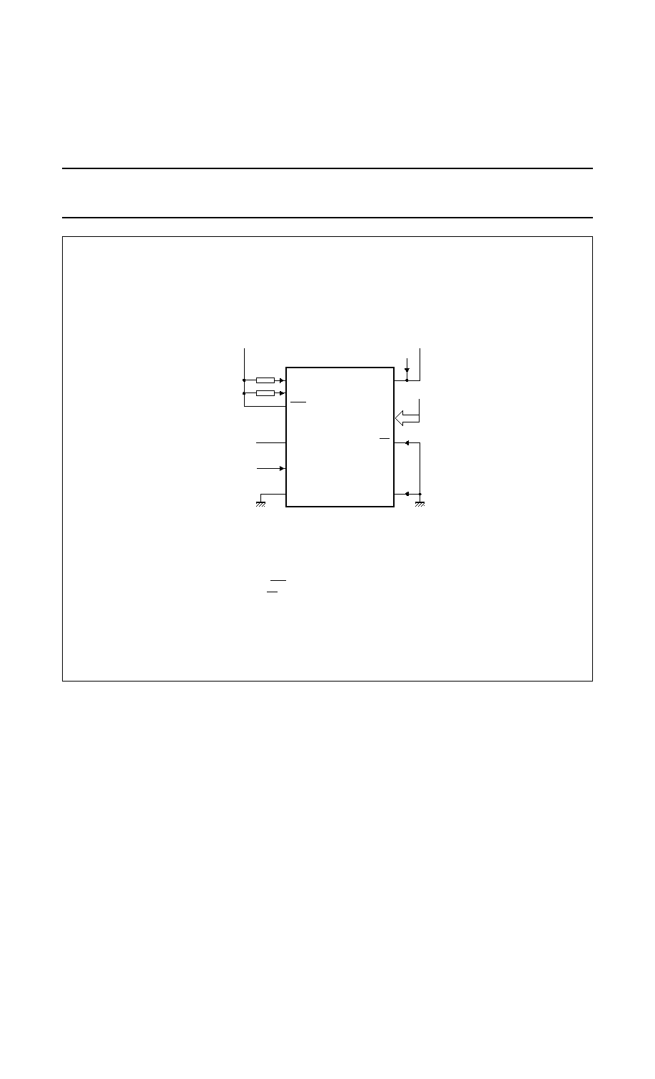
1999 Aug 19
156
Philips Semiconductors
Objective Specification
Single-chip 8-bit microcontroller with CAN controller
P8xC591
Fig.66 I
DD
Test Condition, Power-down Mode.
All other pins are disconnected. V
DD
= 2 V to 5.5 V
(1) The following pins must be forced to V
DD
: Port 0 and RST.
(2) The following pins must be forced to V
SS
: AV
SS
and EA.
(3) Port 1.6 and 1.7 should be connected to V
DD
through resistors of sufficiently high value such that the sink current into these pins cannot exceed
the I
OL1
spec of the pins. These pins must not have logic 0 written to them prior to this measurement.
(4) The following pins must be disconnected: XTAL2 and all pins not specified above.
handbook, full pagewidth
MHI057
P1.6
P1.7
RST
XTAL2
P8xC591
XTAL1
VSS
VDD
IDD
VDD
AVSS
VDD
EA
P0
(n.c.)
CLOCK SIGNAL
VDD

1999 Aug 19
157
Philips Semiconductors
Objective Specification
Single-chip 8-bit microcontroller with CAN controller
P8xC591
25.1
Timing symbol definitions
Oscillator:
f
CLK
= clock frequency
t
CLK
= clock period
Timing symbols (acronyms):
Each timing symbol has five characters. The first character
is always a 't' (= time). the remaining four characters of the
symbol (typed in subscript), depending on their relative
positions, indicate the name of a signal or the logical status
of that signal. the designations are as follows:
A =address
C = clock
D = input data
H = logic level HIGH
I = instruction (program memory contents)
L = Logic level LOW or ALE
P = PSEN
Q = output data
R = RD signal
t = time
V = valid
W = WR signal
X = no longer a valid logic level
Z = float
Examples:
t
AVLL
= time for address valid to ALE LOW
t
LLPL
= time for ALE LOW to PSEN LOW
26 EPROM CHARACTERISTICS
The P8xC591 contains three signature bytes that can be
read and used by an EPROM programming system to
identify the device. The signature bytes identify the device
as an P8xC591 manufactured by Philips:
∑
(030H) = 15H indicates manufactured by Philips
∑
(0031H) = 98H indicates Hamburg
∑
(60H) = 01H indicates P87C591
26.1
Program verification
If security bits 2 or 3 have not been programmed, the
on-chip program memory can be read out for program
verification.
If the encryption table has been programmed, the data
presented at port 0 will be exclusive NOR of the program
byte with one of the encryption bytes. The user will have to
know the encryption table contents in order to correctly
decode the verification data. The encryption table itself
cannot be read out.
26.2
Security bits
With none of the security bits programmed the code in the
program memory can be verified. If the encryption table is
programmed, the code will be encrypted when verified.
When only security bit 1 (see Table 113) is programmed,
MOVC instructions executed from external program
memory are disabled from fetching code bytes from the
internal memory. EA is latched on Reset and all further
programming of the EPROM is disabled. When security
bits 1 and 2 are programmed, in addition to the above,
verify mode is disabled.
When all three security bits are programmed, all of the
conditions above apply and all external program memory
execution is disabled.
Table 113 Program security bits for EPROM devices
P = programmed; U = unprogrammed.
Note
1. Any other combination of the security bits is not defined.
PROGRAM
LOCK BITS
(1)
SB1 SB2 SB3
PROTECTION DESCRIPTION
1
U
U
U
No Program Security features enabled. (Code verify will still be encrypted by the
Encryption Array if programmed.).
2
P
U
U
MOVC instructions executed from external Program Memory are disabled from
fetching code bytes from internal memory, EA is sampled and latched on reset,
and further programming of the EPROM is disabled.
3
P
P
U
Same as 2, also verify is disabled.
4
P
P
P
Same as 3, and external memory execution is disabled.

1999 Aug 19
158
Philips Semiconductors
Objective Specification
Single-chip 8-bit microcontroller with CAN controller
P8xC591
27 PACKAGE OUTLINES
UNIT
A
A
min.
max.
max.
max. max.
1
A
4
b
p
E
(1)
(1)
(1)
e
H
E
Z
y
w
v
REFERENCES
OUTLINE
VERSION
EUROPEAN
PROJECTION
ISSUE DATE
IEC
JEDEC
EIAJ
mm
4.57
4.19
0.51
3.05
0.53
0.33
0.021
0.013
16.66
16.51
1.27
17.65
17.40
0.51
2.16
45
o
0.18
0.10
0.18
DIMENSIONS (millimetre dimensions are derived from the original inch dimensions)
Note
1. Plastic or metal protrusions of 0.01 inches maximum per side are not included.
SOT187-2
D
(1)
16.66
16.51
H
D
17.65
17.40
E
Z
2.16
D
b
1
0.81
0.66
k
1.22
1.07
k
1
0.180
0.165
0.020
0.12
A
3
0.25
0.01
0.656
0.650
0.05
0.695
0.685
0.020
0.085
0.007 0.004
0.007
L
p
1.44
1.02
0.057
0.040
0.656
0.650
0.695
0.685
e
E
e
D
16.00
14.99
0.630
0.590
16.00
14.99
0.630
0.590
0.085
0.032
0.026
0.048
0.042
29
39
44
1
6
7
17
28
18
40
detail X
(A )
3
b
p
w
M
A
1
A
A
4
L
p
b
1
k
1
k
X
y
e
E
B
D
H
E
e
E
H
v
M
B
D
Z D
A
Z E
e
v
M
A
pin 1 index
112E10
MO-047AC
0
5
10 mm
scale
95-02-25
97-12-16
inches
PLCC44: plastic leaded chip carrier; 44 leads
SOT187-2
D
e

Philips Semiconductors
Objective specification
P8xC591
Single-chip 8-bit microcontroller with CAN controller
1999 Aug 19
159
QFP44:
plastic quad flat package; 44 leads (lead length 1.3 mm); body 10 x 10 x 1.75 mm
SOT307-2

1999 Aug 19
160
Philips Semiconductors
Objective Specification
Single-chip 8-bit microcontroller with CAN controller
P8xC591
28 SOLDERING
28.1
Plastic leaded-chip carriers/quad flat-packs
28.1.1
B
Y WAVE
During placement and before soldering, the component
must be fixed with a droplet of adhesive. After curing the
adhesive, the component can be soldered. The adhesive
can be applied by screen printing, pin transfer or syringe
dispensing.
Maximum permissible solder temperature is 260
∞
C, and
maximum duration of package immersion in solder bath is
10 s, if allowed to cool to less than 150
∞
C within 6 s.
Typical dwell time is 4 s at 250
∞
C.
A modified wave soldering technique is recommended
using two solder waves (dual-wave), in which a turbulent
wave with high upward pressure is followed by a smooth
laminar wave. Using a mildly-activated flux eliminates the
need for removal of corrosive residues in most
applications.
28.1.2
B
Y SOLDER PASTE REFLOW
Reflow soldering requires the solder paste (a suspension
of fine solder particles, flux and binding agent) to be
applied to the substrate by screen printing, stencilling or
pressure-syringe dispensing before device placement.
Several techniques exist for reflowing; for example,
thermal conduction by heated belt, infrared, and
vapour-phase reflow. Dwell times vary between 50 and
300 s according to method. Typical reflow temperatures
range from 215 to 250
∞
C.
Preheating is necessary to dry the paste and evaporate
the binding agent. Preheating duration: 45 min at 45
∞
C.
28.1.3
R
EPAIRING SOLDERED JOINTS
(
BY HAND
-
HELD
SOLDERING IRON OR PULSE
-
HEATED SOLDER TOOL
)
Fix the component by first soldering two, diagonally
opposite, end pins. Apply the heating tool to the flat part of
the pin only. Contact time must be limited to 10 s at up to
300
∞
C. When using proper tools, all other pins can be
soldered in one operation within 2 to 5 s at between 270
and 320
∞
C. (Pulse-heated soldering is not recommended
for SO packages.
For pulse-heated solder tool (resistance) soldering of VSO
packages, solder is applied to the substrate by dipping or
by an extra thick tin/lead plating before package
placement.
29 DEFINITIONS
30 LIFE SUPPORT APPLICATIONS
These products are not designed for use in life support appliances, devices, or systems where malfunction of these
products can reasonably be expected to result in personal injury. Philips customers using or selling these products for
use in such applications do so at their own risk and agree to fully indemnify Philips for any damages resulting from such
improper use or sale.
Data sheet status
Objective specification
This data sheet contains target or goal specifications for product development.
Preliminary specification
This data sheet contains preliminary data; supplementary data may be published later.
Product specification
This data sheet contains final product specifications.
Limiting values
Limiting values given are in accordance with the Absolute Maximum Rating System (IEC 134). Stress above one or
more of the limiting values may cause permanent damage to the device. These are stress ratings only and operation
of the device at these or at any other conditions above those given in the Characteristics sections of this specification
is not implied. Exposure to limiting values for extended periods may affect device reliability.
Application information
Where application information is given, it is advisory and does not form part of the specification.

Philips Semiconductors
Objective specification
P8xC591
Single-chip 8-bit microcontroller with CAN controller
1999 Aug 19
160
Definitions
Short-form specification -- The data in a short-form specification is extracted from a full data sheet with the same type number and title.
For detailed information see the relevant data sheet or data handbook.
Limiting values definition -- Limiting values given are in accordance with the Absolute Maximum Rating System (IEC 134). Stress above
one or more of the limiting values may cause permanent damage to the device. These are stress ratings only and operation of the device at
these or at any other conditions above those given in the Characteristics sections of the specification is not implied. Exposure to limiting values
for extended periods may affect device reliability.
Application information -- Applications that are described herein for any of these products are for illustrative purposes only. Philips
Semiconductors make no representation or warranty that such applications will be suitable for the specified use without further testing or
modification.
Disclaimers
Life support -- These products are not designed for use in life support appliances, devices or systems where malfunction of these products
can reasonably be expected to result in personal injury. Philips Semiconductors customers using or selling these products for use in such
applications do so at their own risk and agree to fully indemnify Philips Semiconductors for any damages resulting from such application.
Right to make changes -- Philips Semiconductors reserves the right to make changes, without notice, in the products, including circuits,
standard cells, and/or software, described or contained herein in order to improve design and/or performance. Philips Semiconductors
assumes no responsibility or liability for the use of any of these products, conveys no license or title under any patent, copyright, or mask work
right to these products, and makes no representations or warranties that these products are free from patent, copyright, or mask work right
infringement, unless otherwise specified.
Philips Semiconductors
811 East Arques Avenue
P.O. Box 3409
Sunnyvale, California 94088≠3409
Telephone 800-234-7381
©
Copyright Philips Electronics North America Corporation 1999
All rights reserved. Printed in U.S.A.
Date of release: 09-99
Document order number:
9397 750 06433
Philips
Semiconductors
Data sheet
status
Objective
specification
Preliminary
specification
Product
specification
Product
status
Development
Qualification
Production
Definition
[1]
This data sheet contains the design target or goal specifications for product development.
Specification may change in any manner without notice.
This data sheet contains preliminary data, and supplementary data will be published at a later date.
Philips Semiconductors reserves the right to make changes at any time without notice in order to
improve design and supply the best possible product.
This data sheet contains final specifications. Philips Semiconductors reserves the right to make
changes at any time without notice in order to improve design and supply the best possible product.
Data sheet status
[1]
Please consult the most recently issued datasheet before initiating or completing a design.