Document Outline
- CONTENTS
- 1 FEATURES
- 2 GENERAL DESCRIPTION
- 3 ORDERING INFORMATION
- 4 BLOCK DIAGRAM
- 5 PINNING INFORMATION
- 5.1 Pinning
- 5.2 Pin description
- 6 FUNCTIONAL DESCRIPTION
- 6.1 Special Function Registers (SFRs)
- 6.2 I/O facilities
- 6.3 Timer/event counters
- 6.4 MSK modem
- 6.5 Watchdog Timer
- 6.6 OTP programming
- 6.7 Oscillator circuitry
- 6.8 Emulation
- 6.9 Non-conformance
- 7 LIMITING VALUES
- 8 CHARACTERISTICS
- 9 PACKAGE OUTLINE
- 10 SOLDERING
- 11 DEFINITIONS
- 12 LIFE SUPPORT APPLICATIONS
- 13 PURCHASE OF PHILIPS I 2 C COMPONENTS
DATA SHEET
Product specification
Supersedes data of 1997 Aug 18
File under Integrated Circuits, IC17
1999 Mar 15
INTEGRATED CIRCUITS
P8xCL883; P8xCL884
TELX microcontrollers for CT0
handset/basestation applications

2
Philips Semiconductors
Product specification
TELX microcontrollers for CT0
handset/basestation applications
P8xCL883; P8xCL884
CONTENTS
1
FEATURES
2
GENERAL DESCRIPTION
3
ORDERING INFORMATION
4
BLOCK DIAGRAM
5
PINNING INFORMATION
5.1
Pinning
5.2
Pin description
6
FUNCTIONAL DESCRIPTION
6.1
Special Function Registers (SFRs)
6.2
I/O facilities
6.2.1
Ports
6.2.2
Port I/O configuration
6.2.3
Alternative Port Function Register (ALTP)
6.3
Timer/event counters
6.3.1
Timer T2
6.3.2
Timer/Counter 2 Control Register (T2CON)
6.4
MSK modem
6.5
Watchdog Timer
6.6
OTP programming
6.6.1
OTP programming by a programmer
6.6.2
In-System Programming mode
6.7
Oscillator circuitry
6.7.1
Resonator requirements
6.7.2
Recommended resonator types
6.8
Emulation
6.9
Non-conformance
6.9.1
Programming interface/ Transparent mode
6.9.2
Low Voltage Detection
6.9.3
Edge detection on UART
7
LIMITING VALUES
8
CHARACTERISTICS
9
PACKAGE OUTLINE
10
SOLDERING
10.1
Introduction to soldering surface mount
packages
10.2
Reflow soldering
10.3
Wave soldering
10.4
Manual soldering
10.5
Suitability of surface mount IC packages for
wave and reflow soldering methods
11
DEFINITIONS
12
LIFE SUPPORT APPLICATIONS
13
PURCHASE OF PHILIPS I
2
C COMPONENTS

3
Philips Semiconductors
Product specification
TELX microcontrollers for CT0
handset/basestation applications
P8xCL883; P8xCL884
1
FEATURES
∑
Full static 80C51 CPU; enhanced 8-bit architecture with:
≠ Minimum 6 cycles per instruction (twice as fast as a
standard 80C51 core)
≠ Non-page oriented instructions
≠ Direct addressing
≠ Four 8-byte RAM register banks
≠ Stack depth limited only by available internal RAM
(maximum 256 bytes)
≠ Multiply, divide, subtract and compare instructions.
∑
8-bit ports:
≠ P8xCL883: 3 (19 I/O lines)
≠ P8xCL884: 3 (18 I/O lines).
∑
Program Memory:
≠ P8xCL883/P8xCL884: 8-kbyte One Time
Programmable (OTP).
∑
256-byte RAM
∑
128-byte EEPROM Data Memory, accessed internally
via I
2
C-bus interface (P8xCL884 only)
∑
Amplitude Controlled Oscillator (ACO) suitable for
quartz crystal or ceramic resonator
∑
Improved Power-on/Power-off reset (POR) circuitry
∑
Low Voltage Detection (LVD) with 11 software
programmable levels
∑
Eight interrupts on Port 1:
≠ Edge or level sensitive triggering selectable via
software
≠ Power-saving use for keyboard control.
∑
Twenty source, twenty vector interrupt structure with two
priority levels
∑
Wake-up from Power-down mode via LVD or external
interrupts at Port 1
∑
DTMF generator (P8xCL884 only)
∑
MSK modem including Manchester encoder/decoder
with 2 digital outputs for analog cordless telephones
(standards CT0/CT1/CT1+)
∑
Two standard 16-bit timer/event counters
∑
Additional 16-bit timer/event counter with Capture,
Compare and Auto-reload function
∑
Watchdog Timer
∑
Full duplex enhanced UART with double buffering
∑
I
2
C-bus interface for serial transfer on two lines,
maximum 400 kHz
∑
Very low current consumption
∑
Single supply voltage: 2.7 to 3.6 V
∑
Frequency: 3.58 MHz
∑
Operating temperature:
-
25 to +70
∞
C
∑
28 pin SO package.
2
GENERAL DESCRIPTION
The P8xCL883/P8xCL884 are manufactured in an
advanced CMOS technology. The P8xCL883 is based on
single-chip technology and the P8xCL884 is based on
MCM (Multi-Chip-Module) technology as the EEPROM is
integrated on a separate chip.
The P8xCL883/P8xCL884 are 8-bit microcontrollers
especially suited for low cost analog cordless telephone
applications (CT0, CT1, CT1+ standards). For this
purpose, features like DTMF, EEPROM, MSK modem and
POR/LVD are integrated on-chip.
The device is optimized for low power consumption.
The P8xCL883/P8xCL884 have two software selectable
features for power reduction: Idle and Power-down modes.
In addition, all derivative blocks can switch off their clock if
they are inactive.
The instruction set of the P8xCL883/P8xCL884 is based
on that of the 80C51. The P8xCL883/P8xCL884 also
function as an arithmetic processor having facilities for
both binary and BCD arithmetic plus bit-handling
capabilities. The instruction set consists of over
100 instructions: 49 one-byte, 46 two-byte, and
16 three-byte. Due to the missing port P2, there is no
external data or memory access and the MOVX operations
cannot be used.
This data sheet details the specific properties of the
P8xCL883/P8xCL884; for details of the
P8xCL883/P8xCL884 core and the derivative functions
see the
"TELX family" data sheet and "Data Handbook
IC20; 80C51-based 8-bit Microcontrollers".

4
Philips Semiconductors
Product specification
TELX microcontrollers for CT0
handset/basestation applications
P8xCL883; P8xCL884
3
ORDERING INFORMATION
TYPE NUMBER
OTP TYPE
PACKAGE
NAME
DESCRIPTION
VERSION
P87CL883T/000
Blank OTP
SO28
plastic small outline package; 28 leads;
body width 7.5 mm
SOT136-1
P87CL884T/000
P87CL883T/xxx
Factory-programmed OTP
P87CL884T/xxx
P83CL883T/xxx
Pre-programmed OTP
P83CL884T/xxx
5
Philips Semiconductors
Product specification
TELX microcontrollers for CT0
handset/basestation applications
P8xCL883; P8xCL884
This text is here in white to force landscape pages to be rotated correctly when browsing through the pdf in the Acrobat reader.This text is here in
_
white to force landscape pages to be rotated correctly when browsing through the pdf in the Acrobat reader.This text is here inThis text is here in
white to force landscape pages to be rotated correctly when browsing through the pdf in the Acrobat reader. white to force landscape pages to be ...
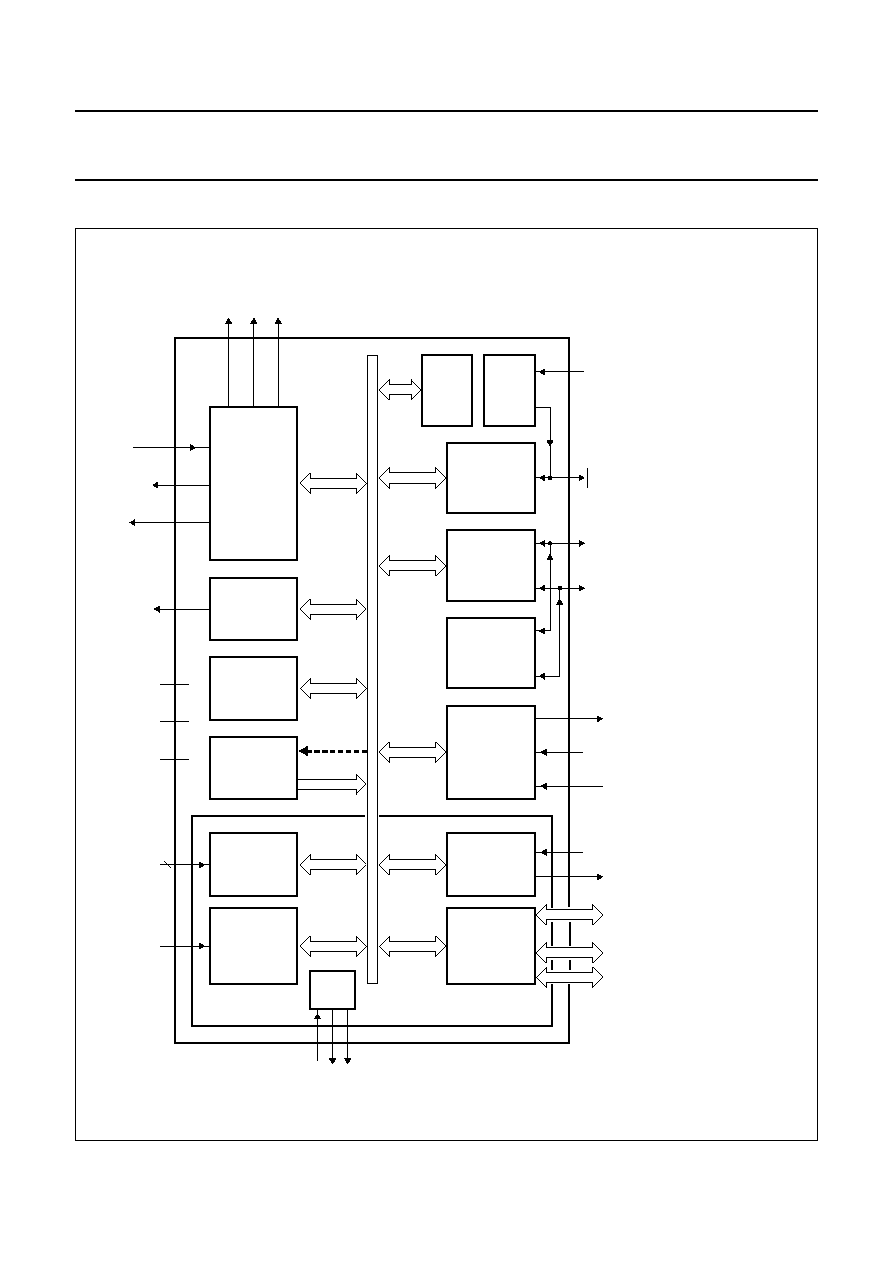
4
BLOCK DIAGRAM
handbook, full pagewidth
MBK981
XTAL1
XTAL2
ACO
TWO 16-BIT
TIMER/
EVENT
COUNTERS
(T0, T1)
CLK
(2)
MOUT2
MOUT1
MOUT0
(3)
PARALLEL
I/O PORTS
P0
P1
P3
(7)
TXD
(4)
T2COMP
(2)
SDA
(2)
SCL
(2)
RXD
(4)
T2
(2)
RST
PORENABLE
T2EX
(2)
CPU
8
SERIAL
UART
PORT
DATA
MEMORY
RAM
DTMF
P87CL883
P87CL884
TONE
(1)
RX_MUTE
(6)
TX_MUTE
(6)
MIN
VDD
VPP
VSS
MSK MODEM
8-bit
internal bus
PROGRAM
MEMORY
OTP/ROM
(5)
16-BIT
TIMER/EVENT
COUNTER WITH
CAPTURE/
COMPARE
(T2)
EEPROM
(1)
I
2
C-BUS
INTERFACE
WATCHDOG
TIMER
(T3)
POR
LVD
T0
(4)
INT2 to INT9
(2)
Fig.1 Block diagram.
(1) Only available on the P8xCL884.
(2) Alternative functions of Port 1.
(3) MOUT0 is the alternative function of P3.1.
(4) Alternative functions of Port 3; T0 is only available on the P8xCL883.
(5) In-circuit OTP programming.
(6) By software, any I/O pin can be used.
(7) Port 3: P3.0, P3.1 and P3.4; P3.4 is only available on the P8xCL883.
6
Philips Semiconductors
Product specification
TELX microcontrollers for CT0
handset/basestation applications
P8xCL883; P8xCL884
5
PINNING INFORMATION
5.1
Pinning
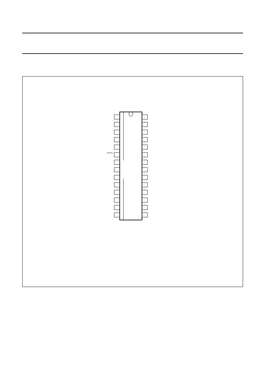
Fig.2 Pin configuration.
handbook, halfpage
MBK005
1
2
3
4
5
6
7
8
9
10
11
12
13
14
28
27
26
25
24
23
22
21
20
19
18
17
16
15
P0.5
PORENABLE/VPP
P0.6
P0.7
P3.0/RXD/data
P3.1/TXD/clock/MOUT0
RST
MIN
MOUT1
MOUT2
XTAL1
XTAL2
P1.0/INT2/T2
P1.1/INT3/T2EX
VDD
P0.4
P0.3
P0.2
P0.1
P0.0
P1.7/INT9/SDA
P1.6/INT8/SCL
P1.5/INT7
P1.4/INT6/CLK
P1.3/INT5
P1.2/INT4/T2COMP
VSS
P3.4/T0 or TONE
(1)
P83CL883
P83CL884
P87CL883
P87CL884
(1) Pin 20: P3.4/T0 on the P8xCL883; TONE on the P8xCL884.

7
Philips Semiconductors
Product specification
TELX microcontrollers for CT0
handset/basestation applications
P8xCL883; P8xCL884
5.2
Pin description
SYMBOL
PIN
DESCRIPTION
RST
6
Active LOW reset. A LOW level on this pin for two machine cycles while the
oscillator is running, resets the device. The RST pin is also an output which can be
used to reset other ICs.
MIN
7
Digital MSK modem input.
MOUT1
8
Digital MSK modem outputs.
MOUT2
9
XTAL1
10
Crystal input. Input to the Amplitude Controlled Oscillator. Also the input for an
externally generated clock source.
XTAL2
11
Crystal output. Output of the Amplitude Controlled Oscillator. To be left
unconnected when an external oscillator clock is used.
V
DD
14
Power supply.
V
SS
15
Ground.
P0.0 to P0.7
23 to 27,
1 to 3
Port 0. 8-bit bidirectional I/O port. Every port pin can be used as open-drain,
standard port, high-impedance input or push-pull output, according to Section 6.2.
P1.0/INT2/T2
12
Port 1. 8-bit bidirectional I/O port with alternative functions. Every port pin except
P1.6 and P1.7 (I
2
C-bus pins) can be used as open-drain, standard port,
high-impedance input or push-pull output, according to Section 6.2. Port P1.3 has
LED drive capability.
Port 1 also serves the alternative functions: INT2 to INT9 interrupts; Timer T2
external inputs T2 and T2EX; Timer T2 compare output T2COMP; external clock
output CLK; I
2
C-bus clock SCL and data in/outputs SDA.
P1.1/INT3/T2EX
13
P1.2/INT4/T2COMP
16
P1.3/INT5
17
P1.4/INT6/CLK
18
P1.5/INT7
19
P1.6/INT8/SCL
21
P1.7/INT9/SDA
22
P3.0/RXD/data
4
Port 3. 3 or 2-bit bidirectional I/O port with alternative functions. Every port pin can
be used as open-drain, standard port, high-impedance input or push-pull output,
according to Chapter 6.2.
Port 3 also serves the alternative functions: RXD/data is the serial port receiver
data input (asynchronous) or data I/O (synchronous); TXD/clock is the serial port
transmitter data output (asynchronous) or clock output (synchronous) or digital
MSK modem output MOUT0; T0 is an external input for Timer 0.
P3.4/T0 is only available on the P8xCL883.
P3.1/TXD/clock/
MOUT0
5
P3.4/T0
20
TONE
20
DTMF output; TONE is only available on the P8xCL884.
PORENABLE/V
PP
28
PORENABLE. Power-on reset circuit enable. If PORENABLE = 1, the internal
Power-on reset circuit is enabled. If external reset circuitry is used, it is
recommended to keep PORENABLE = 0 to reach lowest power consumption. This
pin is also used for the OTP programming voltage V
PP
.
8
Philips Semiconductors
Product specification
TELX microcontrollers for CT0
handset/basestation applications
P8xCL883; P8xCL884
6
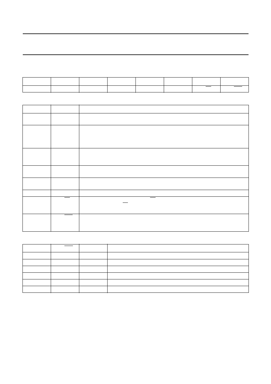
FUNCTIONAL DESCRIPTION
6.1
Special Function Registers (SFRs)
Table 1
List of SFRs
REGISTER
ADDRESS
(HEX)
RESET VALUE
(1)
80C51 core
ACC
E0
0000 0000
B
F0
0000 0000
DPL
82
0000 0000
DPH
83
0000 0000
PCH
no SFR
0000 0000
PCL
no SFR
0000 0000
PCON
87
0000 0000
PRESC
F3
0000 0000
PSW
D0
0000 0000
SP
81
0000 0111
T0/T1
TCON
88
0000 0000
TH0
8C
0000 0000
TH1
8D
0000 0000
TL0
8A
0000 0000
TL1
8B
0000 0000
TMOD
89
0000 0000
Port
ALTP
A3
0000 0000
P0
80
1111 1111
P0CFGA
8E
1111 1111
P0CFGB
8F
0000 0000
P1
90
1111 1111
P1CFGA
9E
0011 1111
P1CFGB
9F
0000 0000
P3
B0
XXX
1
XX
11
P3CFGA
BE
XXX
1
XX
11
P3CFGB
BF
XXX
0
XX
00
P4
C1
XXXX XXX
0
TIMER2
COMP2H
AB
0000 0000
COMP2L
AA
0000 0000
RCAP2H
CB
0000 0000
RCAP2L
CA
0000 0000
T2CON
C8
0000 0000
TH2
CD
0000 0000
TL2
CC
0000 0000
EEPROM interface
EECON
FB
0000 0000
DTMF
HGF
A2
0000 0000
LGF
A1
0000 0000
Interrupt logic
IEN0
A8
0000 0000
IEN1
E8
0000 0000
IEN2
F1
0000 0000
IP0
B8
0000 0000
IP1
F8
0000 0000
IP2
F9
0000 0000
ISE1
E1
0000 0000
IX1
E9
0000 0000
IRQ1
C0
0000 0000
LVD
LVDCON
F2
0000 0000
POR/ACO
RSTAT
E6
XXX
0 1000
MSK
MCON
D3
0000 0000
MBUF
D1
XXXX XXXX
MSTAT
D2
XX
00 0000
UART
S0BUF
99
0000 0000
S0CON
98
0000 0000
I
2
C-bus interface
S1ADR
DB
0000 0000
S1CON
D8
0000 0000
S1DAT
DA
0000 0000
S1STA
D9
1111 1000
REGISTER
ADDRESS
(HEX)
RESET VALUE
(1)

9
Philips Semiconductors
Product specification
TELX microcontrollers for CT0
handset/basestation applications
P8xCL883; P8xCL884
Note
1. Where: X = undefined state or not implemented bit.
6.2
I/O facilities
6.2.1
P
ORTS
The P8xCL883/P8xCL884 have 19 and 18 I/O lines
respectively, treated as 19 and 18 individually addressable
bits or as three parallel 8-bit addressable ports.
The alternative functions are detailed below:
Port 0 Offers no alternative functions.
Port 1 Used for a number of special functions:
∑
P1.0 to P1.7 provides the inputs for the external
interrupts INT2 to INT9
∑
P1.2/T2COMP for external activation and
Compare/Auto-reload output function of Timer 2
∑
P1.4/CLK for the clock output
∑
P1.6/SCL and P1.7/SDA for the I
2
C-bus interface
are real open-drain outputs or high-impedance;
no other port configurations are available.
Port 2 Not available.
Port 3 Pins can be configured individually to provide:
∑
P3.0/RXD/data and P3.1/TXD/clock/MOUT0
which are serial port receiver input and
transmitter output (UART)
∑
P3.4/T0 as counter input; available only in
P8xCL883.
To enable a Port pin alternative function, the Port bit latch
in its SFR must contain a logic 1.
WDT
WDCON
A5
1010 0101
WDTIM
FF
0000 0000
OTP interface
OAH
D5
X
00
X XXXX
OAL
D4
XXXX XXXX
ODATA
D6
XXXX XXXX
OISYS
DC
000
X
0000
OTEST
D7
0000 0000
Reserved locations; do not write
reserved
E7, FD
-
REGISTER
ADDRESS
(HEX)
RESET VALUE
(1)
Each port consists of a latch (Special Function Registers
P0 to P3), an output driver and input buffer. All ports have
internal pull-ups. Figure 3b shows that the strong
transistor `p1' is turned on for only one oscillator period
after a LOW-to-HIGH transition in the port latch. When on,
it turns on `p3' (a weak pull-up) through the inverter IN1.
This inverter and transistor `p3' form a latch which holds
the logic 1.
Port P1.3 has LED drive capability.
6.2.2
P
ORT
I/O
CONFIGURATION
I/O port output configurations are determined by the
settings in port configuration SFRs. There are 2 SFRs for
each port: PnCFGA and PnCFGB, where `n' indicates the
specific port number (0 to 3). One bit in each of the 2 SFRs
relates to the output setting for the corresponding port pin,
allowing any combination of the 2 output types to be mixed
on those port pins. For example, the output type of P1.3, is
controlled by the setting of bit 3 in the SFRs P1CFGA and
P1CFGB.
The port pins may be individually configured via SFRs with
one of the following modes (P1.6 and P1.7 can be
open-drain or high-impedance but never have any diodes
against V
DD
). These modes are also shown in Fig.3.
Mode 0 Open-drain; quasi-bidirectional I/O with
n-channel open-drain output. Use as an output
requires the connection of an external pull-up
resistor; e.g. Port 0 for external memory
accesses (EA = 0) or access above the built-in
memory boundary. The ESD protection diodes
against V
DD
and V
SS
are still present; see Fig.3b.
Except for the I
2
C-bus pins P1.6 and P1.7, ports
which are configured as open-drain still have a
protection diode to V
DD
.
Mode 1 Standard port; quasi-bidirectional I/O with
pull-up. The strong pull-up `p1' is turned on for
only two oscillator periods after a LOW-to-HIGH
transition in the port latch. After these two
oscillator periods the port is only weakly driven
through `p2' and `very weakly' driven through `p3'
(see Fig.3b).
Mode 2 High-impedance; this mode turns off all output
drivers on a port. Thus, the pin will not source or
sink current and may be used as an input-only pin
with no internal drivers for an external device to
overcome (see Fig.3c).
Mode 3 Push-pull; output with drive capability in both
polarities. Under this mode, pins can only be
used as outputs (see Fig.3d).
10
Philips Semiconductors
Product specification
TELX microcontrollers for CT0
handset/basestation applications
P8xCL883; P8xCL884
Tables 2 and 3 show the configuration register settings for
the 4 port output types.
The electrical characteristics of each output type can be
found in Chapter 8. The default port configuration after
reset is given in Table 3.
Table 2
Port Configuration Registers PnCFGA and PnCFGB (n = 0 to 3) settings
Note
1. Mode changes may cause glitches to occur during transitions. When modifying both registers, WRITE instructions
should be carried out consecutively.
Table 3
Special Function Registers for port configurations/data
Notes
1. This means that P0, P1.0 to P1.5 and P3 are initialized in Mode 1 (quasi-bidirectional, driving a weak HIGH) and the
I
2
C-bus ports P1.6 and P1.7 are initialized in Mode 0 (open-drain, not driven).
2. Port pin P3.4 is only available on P8xCL883.
MODE
(1)
PnCFGA
PnCFGB
PORT OUTPUT MODE
NORMAL PORTS
I
2
C-BUS PORTS (P1.6 AND P1.7)
Mode 0
0
0
open-drain
open-drain
Mode 1
1
0
quasi-bidirectional
open-drain
Mode 2
0
1
high-impedance
high-impedance
Mode 3
1
1
push-pull
open-drain
REGISTER NAME
REGISTER MNEMONIC
SFR ADDRESS (HEX)
STATE AFTER RESET
Port P0 output data
(1)
P0
80
1111 1111
Port P0 configuration A
P0CFGA
8E
1111 1111
Port P0 configuration B
P0CFGB
8F
0000 0000
Port P1 output data
(1)
P1
90
1111 1111
Port P1 configuration A
P1CFGA
9E
0011 1111
Port P1 configuration B
P1CFGB
9F
0000 0000
Port P3 output data
(1)
P3
B0
XXX
1
XX
11
(2)
Port P3 configuration A
P3CFGA
BE
XXX
1
XX
11
(2)
Port P3 configuration B
P3CFGB
BF
XXX
0
XX
00
(2)
11
Philips Semiconductors
Product specification
TELX microcontrollers for CT0
handset/basestation applications
P8xCL883; P8xCL884
6.2.3
A
LTERNATIVE
P
ORT
F
UNCTION
R
EGISTER
(ALTP)
This 4-bit register selects the alternative function of certain port pins.
Table 4
Alternative Port Function Register (SFR address A3H)
Table 5
Description of ALTP bits
7
6
5
4
3
2
1
0
-
-
-
-
EMOUT0
ECLK
EMLDY
ETONE
BIT
SYMBOL
DESCRIPTION
7 to 4
-
These 4 bits are reserved.
3
EMOUT0
If this bit is set, P3.1 will output the MOUT0 signal.
2
ECLK
If this bit is set, P1.4 is configured to be push-pull, and P1.4 will output the system clock.
1
EMLDY
If this bit is set, P1.5 is configured to be push-pull, and P1.5 will output the digital MLDY
signal of the DTMF generator.
0
ETONE
If this bit is set, the TONE output of the DTMF generator is enabled.
12
Philips Semiconductors
Product specification
TELX microcontrollers for CT0
handset/basestation applications
P8xCL883; P8xCL884
Fig.3 Port configuration options.
handbook, full pagewidth
MBK004
this diode is not
implemented
on the I
2
C-bus pins
VSS
VDD external
n
Q
from port latch
external
pull-up
I/O pin
input data
VDD
VSS
handbook, full pagewidth
MBK001
p1
p2
p3
input data
1 oscillator
period
n
VSS
VDD
strong pull-up
I/O pin
Q
from port latch
IN1
VSS
handbook, full pagewidth
MBK002
this diode is not
implemented
on the I
2
C-bus pins
input data
VDD
I/O pin
VSS
handbook, full pagewidth
MBK003
p
n
strong pull-up
Q
from port latch
VSS
VDD
VDD
I/O pin
input data
VSS
a. Open-drain.
b. Standard/quasi-bidirectional.
c. High-impedance.
d. Push-pull.

13
Philips Semiconductors
Product specification
TELX microcontrollers for CT0
handset/basestation applications
P8xCL883; P8xCL884
6.3
Timer/event counters
The P8xCL883/P8xCL884 contain three 16-bit timer/event
counters: Timer 0, Timer 1 and Timer 2 which can perform
the following functions:
∑
Measure time intervals and pulse durations
∑
Count events
∑
Generate interrupt requests
∑
Generate output on comparator match.
In the `timer' mode the register is incremented every
machine cycle.
Since a machine cycle consists of minimum 6 oscillator
periods, the maximum count rate is
1
/
6
f
osc
.
In the `counter' mode, the register is incremented in
response to a HIGH-to-LOW transition. Since it takes one
machine cycle (minimum 6 oscillator periods) to recognize
a HIGH-to-LOW transition, the maximum count rate is
1
/
6
f
osc
. To ensure a given level is sampled, it should be held
for at least one complete machine cycle.
Timer 0 and Timer 1 can be programmed independently to
operate in four modes:
Mode 0 8-bit timer or 8-bit counter each with
divide-by-32 prescaler.
Mode 1 16-bit time-interval or event counter.
Mode 2 8-bit time-interval or event counter with automatic
reload upon overflow.
Mode 3 Timer 0 establishes TL0 and TH0 as two
separate counters.
Note that the T0 input is only available on P8xCL883.
6.3.1
T
IMER
T2
Note that the timer T2 of the P8xCL883/P8xCL884
deviates from the timer T2 described in the
"TELX
family" data sheet.
Timer T2 is a 16-bit timer/counter that can operate either
as a timer or as an event counter. These functions are
selected by the state of the C/T2 bit in the T2CON register.
Five operating modes are available:
∑
Capture
∑
Compare
∑
Auto-reload
∑
Compare with Auto-reload
∑
Capture and Compare.
These modes are selected via the T2CON register.
6.3.1.1
Capture mode
In the Capture mode, two options may be selected by the
EXEN2 bit in T2CON:
∑
If EXEN2 = 0, then Timer 2 is a 16-bit timer or counter
which upon overflowing sets the Timer 2 overflow bit
TF2, this may then be used to generate an interrupt.
∑
If EXEN2 = 1, Timer 2 operates as described above but
with the additional feature that a HIGH-to-LOW
transition at external input T2EX causes the current
value in TL2 and TH2 to be captured into registers
RCAP2L and RCAP2H respectively. In addition, the
transition at T2EX causes the EXF2 bit in T2CON to be
set; this may also be used to generate an interrupt.
The Capture mode is shown in Fig.4.
6.3.1.2
Compare mode
In the Compare mode, each time timer T2 is incremented,
the contents of the compare registers COMP2H and
COMP2L is compared with the new counter value of
timer T2. When a match occurs, the interrupt flag COMP in
register T2CON and port bit P1.2 are toggled. The 16-bit
value held in these registers is preset by software. The first
toggle after a chip reset will set the flag COMP.
The Compare mode is shown in Fig.4.
6.3.1.3
Auto-reload mode
In the Auto-reload mode there are also two options
selected by the EXEN2 bit in T2CON:
∑
If EXEN2 = 0, then when Timer 2 rolls over, it sets the
TF2 bit but also causes the Timer 2 registers to be
reloaded with the 16-bit value held in registers RCAP2L
and RCAP2H. The 16-bit value held in these registers is
preset by software.
∑
If EXEN2 = 1, Timer 2 operates as described above but
with the additional feature that a HIGH-to-LOW
transition at external input T2EX will also trigger the
16-bit reload and set the EXF2 bit.
6.3.1.4
Compare with Auto-reload mode
The Auto-reload mode can also be used together with the
Compare mode. The Auto-reload modes are shown in
Fig.5.
6.3.1.5
Capture and Compare modes
The Capture and the Compare mode of timer T2 can be
used separately or simultaneously. The function is chosen
via the bits ECOMP, CP/RL2 and TR2 in register T2CON.
14
Philips Semiconductors
Product specification
TELX microcontrollers for CT0
handset/basestation applications
P8xCL883; P8xCL884
Fig.4 Timer 2 in Capture and/or Compare mode.
handbook, full pagewidth
MBH998
TL2
(8 BITS)
COMPARATOR 1
(16 BITS)
TR2
control
TH2
(8 BITS)
COMP2L
COMP2H
ECOMP
RCAP2L
RCAP2H
EXF2
TF2
COMP
Timer 2
interrupt
port
P1.2
EXEN2
control
C/T2 = 1
T2 pin
6
OSC
transition
detector
T2EX pin
C/T2 = 0
capture
Fig.5 Timer 2 in Auto-Reload with/without Compare mode.
handbook, full pagewidth
MBH999
TL2
(8 BITS)
COMPARATOR 1
(16 BITS)
TR2
control
TH2
(8 BITS)
COMP2L
COMP2H
ECOMP
RCAP2L
RCAP2H
EXF2
TF2
COMP
Timer 2
interrupt
port
P1.2
EXEN2
control
C/T2 = 1
T2 pin
6
OSC
transition
detector
T2EX pin
C/T2 = 0
reload
15
Philips Semiconductors
Product specification
TELX microcontrollers for CT0
handset/basestation applications
P8xCL883; P8xCL884
6.3.2
T
IMER
/C
OUNTER
2 C
ONTROL
R
EGISTER
(T2CON)
Table 6
Timer/Counter 2 Control Register (SFR address C8H)
Table 7
Description of T2CON bits
Table 8
Timer 2 operating modes
7
6
5
4
3
2
1
0
TF2
EXF2
COMP
ECOMP
EXEN2
TR2
C/T2
CP/RL2
BIT
SYMBOL
DESCRIPTION
7
TF2
Timer 2 overflow flag. TF2 is set by a Timer 2 overflow and must be cleared by
software.
6
EXF2
Timer 2 external flag. EXF2 is set when either a capture or reload is caused by a
negative transition on T2EX and when EXEN2 = 1. When Timer T2 interrupt is enabled,
EXF2 = 1 will cause the CPU to vector to Timer 2 interrupt routine. EXF2 must be
cleared by software.
5
COMP
Interrupt flag. When a match between the 16-bit compare register (COMP2L and
COMP2H) and the new counter value of timer T2 occurs, the interrupt flag COMP in
register T2CON and port bit P1.2 are toggled.
4
ECOMP
Enable compare output bit. When set by software, the controller toggles port bit P1.2
(T2COMP) when a compare match occurs.
3
EXEN2
Timer 2 external enable flag. When set, allows a capture or reload to occur as a result
of a negative transition on T2EX. EXEN2 = 0 causes Timer 2 to ignore events at T2EX.
2
TR2
Timer 2 start/stop control. Control bit for Timer 2.
1
C/T2
Timer 2 timer or counter select. C/T2 = 0 selects the internal timer with a clock
frequency of
1
/
6
f
osc
. C/T2 = 1 selects the external event counter; negative
edge-triggered.
0
CP/RL2
Capture/reload flag. When set captures will occur on negative transitions at T2EX, if
EXEN2 = 1. When cleared, auto-reloads will occur either with Timer 2 overflows or
negative transitions at T2EX when EXEN2 = 1.
ECOMP
CP/RL2
TR2
MODE
0
0
1
16-bit Auto-reload
0
1
1
16-bit Capture
1
0
1
16-bit Compare
1
1
1
16-bit Capture and Compare
1
0
0
16-bit Compare with Auto-reload
0
0
0
off

16
Philips Semiconductors
Product specification
TELX microcontrollers for CT0
handset/basestation applications
P8xCL883; P8xCL884
6.4
MSK modem
For the P8xCL883/P8xCL884, MIN is no longer the
alternative function of P4.0, but MIN is a separate pin.
The polarity of MIN can however still be programmed with
the P4.0 bit. P4.0 is a data SFR but no port logic is
connected.
Only the most significant bits of MOUT, i.e. MOUT2 and
MOUT1 are directly available as separate pins. In order to
be able to further increase the signal quality, the MOUT0
signal is available as an alternative port function of P3.1.
For controlling this alternative port function the EMOUT0
bit has been added to the Alternative Port Function
Register (ALTP); see Section 6.2.3.
6.5
Watchdog Timer
The Watchdog Timer differs from the description in the
"TELX family" data sheet in that the external EW pin does
not exist on the P8xCL883/P8xCL884.
Fig.6 Functional diagram of the Watchdog Timer (T3).
handbook, full pagewidth
MBH997
PRESCALER
13-BIT
COUNTER REGISTER
8-BIT
WDTIM
8-BIT RELOAD REGISTER
internal reset
RST pin
fosc
8192
fosc
WDCON
REGISTER
enable
overflow
internal bus
17
Philips Semiconductors
Product specification
TELX microcontrollers for CT0
handset/basestation applications
P8xCL883; P8xCL884
6.6
OTP programming
6.6.1
OTP
PROGRAMMING BY A PROGRAMMER
The 8 kbytes One Time Programmable (OTP) memory
can be programmed by using a programmer (OM4260)
together with a programmer adapter OM5508. Since the
memory is programmable only once, programming an
already programmed address results in a logical AND of
the old and new code. The OTP code can be read out by
the programmer for verification.
6.6.1.1
Signature bytes
The OTP memory contains three signature bytes which
can be read by the programmer to identify the device.
A special address space has been used for these bytes
which does not influence the user address space.
The values of the signature bytes are:
(030H) = 15H, indicates manufactured by Philips
Semiconductors
(031H) = C5H, indicates P8xCL883/P8xCL884
(060H) = 00H, currently not used.
6.6.2
I
N
-S
YSTEM
P
ROGRAMMING MODE
In the In-System Programming mode the OTP can be
programmed under control of the CPU. A program to
control programming has to be available in the OTP. This
mode can be used to program several bytes in the OTP if
the chip is already in a system e.g. to store tuning
parameters.
In the In-System Programming mode the complete
address space OTP can be programmed.
The user should take care not to overwrite the existing
code.
For In-System Programming four SFRs are used to control
the OTP.
Table 9
SFRs for In-System Programming
SFR NAME
DESCRIPTION
OAH
OTP Address High Register
OAL
OTP Address Low Register
ODATA
OTP Data Register
OISYS
OTP In-System Register
6.6.2.1
OTP In-System Programming Register (OISYS)
The OISYS SFR controls the In-System Programming mode. The data that has to be programmed is stored in the SFR
ODATA and the address for this data is held in the SFRs OAH and OAL.
Table 10 OTP In-System Programming Register (SFR address DCH)
Table 11 Description of OISYS bits
7
6
5
4
3
2
1
0
-
-
-
VPon
SEC
SIG
WE
InSysMode
BIT
SYMBOL
DESCRIPTION
7 to 5
-
These bits are reserved.
4
VPon
V
PP
status (read only).
3
-
This bit is reserved.
2
SIG
Signature bytes enable.
1
WE
Write Enable, enables programming.
0
InSysMode
In-System Programming status bit.

18
Philips Semiconductors
Product specification
TELX microcontrollers for CT0
handset/basestation applications
P8xCL883; P8xCL884
6.6.2.2
Mode entry
The In-System Programming mode is entered by setting
the InSysMode bit of the OISYS SFR. The I
2
C-bus is used
for data transfer in this mode. If the I
2
C-bus interface is
addressed by an external master, the interface generates
an interrupt request. The interrupt handler can now read
the OISYS SFR and determine the status of the external
high voltage (VPon). If high voltage is not present the
interrupt is a standard I
2
C-bus interrupt.
If high voltage is present the In-System Program interrupt
routine has to start that writes the InSysMode bit
(OISYS.0) and controls the address and data transfer.
This paragraph is valid for version 2 (`2' ending on
type number). During In-System Programming the OTP
memory must be in the DC read mode. This is achieved by
writing 08H to the OTEST SFR. If the In-System
Programming mode is left, 00H must be written into the
OTEST SRF.
The program voltage must be available and stable for at
least 10
µ
s before the mode is entered and has to be
stable until the circuit has left the In-System Programming
mode. The high voltage can be applied for maximum
60 seconds during the complete lifetime of the circuit.
6.6.2.3
Program cycle
The data and address must be supplied to the
microcontroller and the control program must write to the
SFRs: ODATA, OAH and OAL. A timer has to be initialized
for a 100
µ
s cycle and the WE bit of the OISYS SFR must
be set. Now the core has to be set into Idle mode. As long
as the circuit is in idle mode a programming pulse is
applied. After the interrupt request of the timer the OTP is
available for normal code fetching.
The address applied to the OAH and OAL SFRs must be
in the 8 kbytes address space.
6.6.2.4
Verify for In-System Programming
Verify is done in similar way as programming. The circuit
is put into Idle mode and at the start of this mode the sense
amplifiers are switched to verify mode and a read cycle is
started. The timer must be initialized for a cycle of at least
1
µ
s. The address is supplied by the SFRs OAH and OAL.
The WE bit of the OISYS SFR has to be reset. The OTP
output data is latched in the ODATA SFR. After Idle mode
is finished this SFR can be read in a normal way.
To ensure that the verified data is written into the SFR it is
advised to write FFH into the ODATA SFR before a verify
is started.
6.6.2.5
Signature bytes
The signature bytes can be read by setting the SIG bit of
the OISYS SFR and applying the address of the signature
byte. Applying a write pulse while the SIG bit of the OISYS
SFR is HIGH is forbidden although the contents of the
signature bytes will never be destroyed.
6.6.2.6
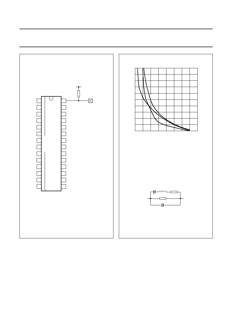
How to connect the PORENABLE/V
PP
pin in
the In-System Programming mode
If the V
PP
pin is dual-mode (e.g. PORENABLE/V
PP
), ICs
connected to the signal PORENABLE must be able to
withstand up to 13 V, i.e. cannot have clamping diodes or
low break-down voltages. If the pin is connected to a fixed
voltage (V
DD
or V
SS
) there must be a way of switching-off
this connection on the PCB. One possible implementation
is presented in Fig.7 where POR is enabled in normal
mode of operation (pin PORENABLE/V
PP
= 1 by the
pull-up), the V
PP
source must supply enough current in R
p
in order to guarantee a minimum 12.5 V on the
PORENABLE/V
PP
pin.
Note that if in the application the Power-on reset is
disabled (pin PORENABLE/V
PP
= 0), applying a high
voltage to the PORENABLE/V
PP
pin will also enable the
POR circuit. This will cause a reset independent of the
actual V
DD
value.
6.7
Oscillator circuitry
General information on the oscillator circuitry can be found
in the
"TELX family" data sheet.
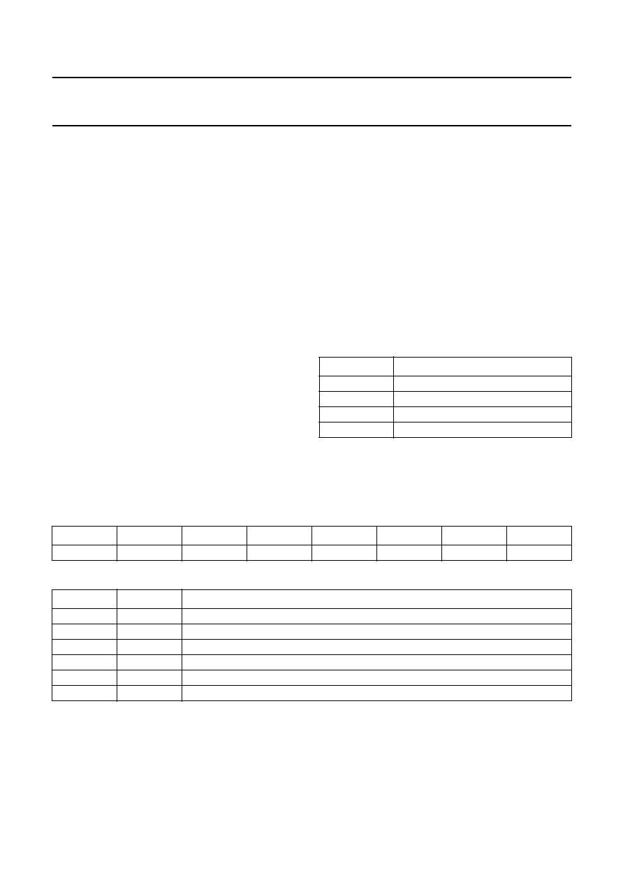
6.7.1
R
ESONATOR REQUIREMENTS
For correct function of the oscillator, the values of R
1
and
C
0
of the chosen resonator (quartz or PXE) must be below
the line shown in Fig.8a. The value of the parallel resistor
R
0
must be less than 47 k
.
The wiring between chip and resonator should be kept as
short as possible.
6.7.2
R
ECOMMENDED RESONATOR TYPES
∑
CSA 3.58MG (supplier Murata)
∑
FCR3.58M5 (supplier TDK).
19
Philips Semiconductors
Product specification
TELX microcontrollers for CT0
handset/basestation applications
P8xCL883; P8xCL884
Fig.7
PORENABLE/V
PP
connection on a PCB.
handbook, halfpage
MBK006
1
2
3
4
5
6
7
8
9
10
11
12
13
14
28
27
26
25
24
23
22
21
20
19
18
17
16
15
P83CL883
P83CL884
P87CL883
P87CL884
VDD
Rp
VPP pad on PCB
a. Resonator curves.
b. Resonator equivalent circuit.
handbook, halfpage
0
(1)
(2)
Co (pF)
20
40
80
500
0
R1
(
)
400
60
300
200
100
MDA088
(3)
C
1e
and C
2e
are the external load capacitances; normally not needed
due to integrated load capacitances of typically 10 pF.
(1) C
1e
= C
2e
= 22 pF.
(2) C
1e
= C
2e
= 0 pF.
(3) C
1e
= C
2e
= 12 pF.
Fig.8 Resonator requirements for the ACO.
handbook, halfpage
C1
C0
L1
R1
R0
MGL137

20
Philips Semiconductors
Product specification
TELX microcontrollers for CT0
handset/basestation applications
P8xCL883; P8xCL884
6.8
Emulation
The emulator for the P8xCL883/P8xCL884 uses the P87CL880 microcontroller in emulation mode. The P87CL880 is a
super-set of the P8xCL883/P8xCL884, i.e. it contains all the functions of the P8xCL883/P8xCL884 plus a number of
other additional functions. It should be noted that some functional differences between P87CL880 and
P8xCL883/P8xCL884 exist; see Table 12.
Table 12 Differences between functions existing in P87CL880 and P8xCL883/P8xCL884
FUNCTION
P87CL880
P8XCL883/P8XCL884
Timer 2
see P87CL880 specification
see P8xCL883/P8xCL884 specification
OTP Program Memory
32 kbytes AFPROM
8 kbytes EPROM or pre-programmed ROM
RAM
512 bytes
256 bytes
EW pin (Watchdog enable)
yes
no
Security concept
see P87CL880 specification
see P8xCL883/P8xCL884 specification
In-System Programming
no
yes
Reset value of SFRs
see P87CL880 specification
see P8xCL883/P8xCL884 specification
POR
hardware programmable
fixed
Frequency
DC to 12.5 MHz
3.58 MHz
Package
QFP64
SO28
6.9
Non-conformance
6.9.1
P
ROGRAMMING INTERFACE
/T
RANSPARENT MODE
The Transparent mode is a special operating mode of the
microcontroller used for parallel and In-System OTP
programming.
For certain combinations of data written to Port 1 (used for
control signal during parallel programming mode) the
Transparent mode may be incorrectly active during normal
operation of the microcontroller. In this case, a transition
on any of Port 0 pins can influence the read out of the
on-chip program memory, resulting in incorrect code
execution.
To avoid this problem, the InSysMode bit in the OTP
In-System Programming Register (SFR address DCH)
must be set in the start-up sequence of the program code.
Apart from preventing incorrect operation as described
above, the setting of this bit does not affect the normal
operation.
6.9.2
L
OW
V
OLTAGE
D
ETECTION
The LVDI bit (LVDCON.6) may incorrectly be set due to a
glitch on the LVD output, when the LVD is enabled, by
changing the bits LVDCON(3:0) from `0000' to any value
within the range `0001' to `0101'. If bit EA in register IEN0
is enabled, an unwanted interrupt may occur.
A software workaround for this problem exists. During the
initialisation sequence:
∑
Enable LVD by writing to register LVDCON
∑
Enable LVD interrupt by writing to register IEN2
∑
Clear the LVDI bit by writing to LVDCON a second time
∑
Set bit EA in register IEN0 (ensures LVDI to be cleared
after initialisation).
6.9.3
E
DGE DETECTION ON
UART
In receive mode 1, 2 and 3 it is possible that an internal
setup/hold condition of a flip-flop is violated. This results in
a not detected start bit (start condition) during receive
mode. The probability of occurrence (verified on sampling
basis) is below 3%.
There is no workaround for this problem other than to use
the UART only in Mode 0 for reception.
21
Philips Semiconductors
Product specification
TELX microcontrollers for CT0
handset/basestation applications
P8xCL883; P8xCL884
7
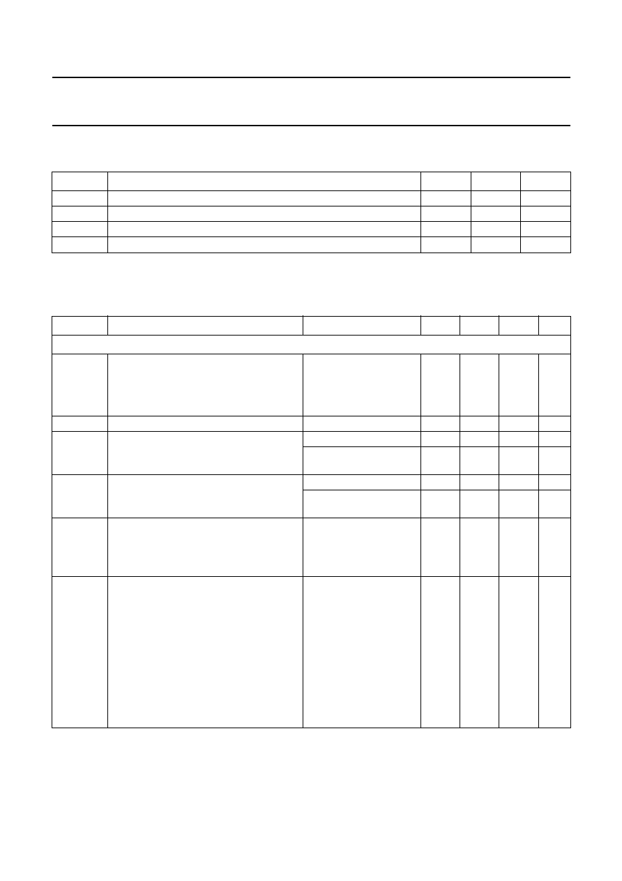
LIMITING VALUES
In accordance with the Absolute Maximum Rating System (IEC 134).
8
CHARACTERISTICS
V
DD
= 2.7 to 3.6 V; V
SS
= 0 V; f
xtal
= 3.58 MHz; T
amb
=
-
25 to +70
∞
C;
T
amb
(during In-System Programming) = +20 to +40
∞
C; all voltages with respect to V
SS
unless otherwise specified.
SYMBOL
PARAMETER
MIN.
MAX.
UNIT
V
DD
supply voltage
-
0.5
+4.0
V
V
I
input voltage on any pin with respect to ground (V
SS
)
-
0.5
V
DD
+ 0.5 V
P
tot
total power dissipation
-
800
mW
T
stg
storage temperature
-
65
+150
∞
C
SYMBOL
PARAMETER
CONDITIONS
MIN.
TYP.
MAX.
UNIT
Supply
V
DD
supply voltage
operating
2.7
-
3.6
V
RAM data retention in Power-down mode
1.0
-
3.6
V
In-System Programming
3.0
-
3.6
V
V
PP
OTP programming voltage
12.5
-
13.0
V
I
DD
operating supply current
V
DD
= 3 V; note 1
-
-
3.0
mA
V
DD
= 3 V; T
amb
= 25
∞
C;
note 1; see Fig.10
-
1.8
-
mA
I
DD(id)
supply current Idle mode
V
DD
= 3 V; note 2
-
-
0.55
mA
V
DD
= 3 V; T
amb
= 25
∞
C;
note 2; see Fig.11
-
0.38
-
mA
I
DD(pd)
supply current Power-down mode
V
DD
= 3 V; T
amb
= 25
∞
C;
note 3; see Fig.12
POR and LVD enabled
-
2
5
µ
A
POR and LVD disabled
-
100
-
nA
I
DD(block)
supply current per block:
V
DD
= 3 V; T
amb
= 25
∞
C;
notes 4 and 5
EEPROM erase/write
-
460
-
µ
A
DTMF
no load on TONE output
-
240
-
µ
A
MSK modem
-
140
-
µ
A
Watchdog
-
110
-
µ
A
I
2
C-bus
-
90
-
µ
A
UART
-
90
-
µ
A
Timer T2
-
90
-
µ
A
Timer T0 or T1
-
5
-
µ
A

22
Philips Semiconductors
Product specification
TELX microcontrollers for CT0
handset/basestation applications
P8xCL883; P8xCL884
Inputs (Ports, MIN, RST, MOUT0 to MOUT2, PORENABLE)
V
IL
LOW-level input voltage
notes 6 and 7
0
-
0.2V
DD
V
V
IH
HIGH-level input voltage
note 6
0.8V
DD
-
V
DD
V
I
IL
LOW-level input current (ports in Mode 1)
V
IN
= 0.4 V; note 8;
see Fig.9
-
10
50
µ
A
I
IL(T)
LOW-level input current; HIGH-to-LOW
transition (ports in Mode 1)
V
IN
= 0.5V
DD
; note 8;
see Fig.9
-
200
1000
µ
A
I
LI
input leakage current (ports in Mode 0 or 2) V
SS
V
I
V
DD
-
-
1
µ
A
Port outputs (Ports, RST, MOUT0 to MOUT2)
I
OL
LOW-level output current; except P1.3,
SDA, SCL and MOUT2
V
OL
= 0.4 V
2
-
-
mA
I
OL1
LOW-level output current; P1.3 (for LED)
V
OL
= 0.4 V
6
-
-
mA
I
OL2
LOW-level output current; SDA, SCL and
MOUT2
V
OL
= 0.4 V; note 9
3
-
-
mA
I
OH
HIGH-level output current except P1.3;
push-pull options only
V
OH
= V
DD
-
0.4 V
2
-
-
mA
I
OH1
HIGH-level output current P1.3
(for LED); push-pull options only
V
OH
= V
DD
-
0.4 V
6
-
-
mA
I
OH2
HIGH-level output current MOUT2
V
OH
= V
DD
-
0.4 V
3
-
-
mA
I
RST
RST pull-up transistor current
V
DD
= 3 V;
V
OH
= V
DD
-
0.4 V
0.05
0.2
-
µ
A
V
DD
= 3 V; V
OH
= V
SS
-
0.6
2.5
µ
A
Power-on reset (POR); for the LVD (Low Voltage Detection) see note 10
V
PORH
Power-on reset trip level HIGH
option 5 in
"TELX family"
specification
2.13
2.37
2.61
V
V
PORL
Power-on reset trip level LOW
option A in
"TELX
family" specification
1.98
2.27
2.56
V
TONE output (note 11 and Fig.13)
V
HG(rms)
HGF voltage (RMS)
V
DD
= 3 V
158
181
205
mV
V
LG(rms)
LGF voltage (RMS)
125
142
160
mV
f/f
frequency deviation
-
0.6
-
+0.6
%
V
DC
DC voltage level
-
0.5V
DD
-
V
V
G
pre-emphasis of group
1.5
2.0
2.5
dB
THD
total harmonic distortion
V
DD
= 3 V; T
amb
= 25
∞
C;
notes 5 and 12
-
25
-
dB
EEPROM (notes 5 and 13)
t
E/W
erase/write time
8
10
12
ms
N
E/W
erase/write cycles
10
5
-
-
t
DR
data retention time
T
amb
= +70
∞
C
10
-
-
years
SYMBOL
PARAMETER
CONDITIONS
MIN.
TYP.
MAX.
UNIT
23
Philips Semiconductors
Product specification
TELX microcontrollers for CT0
handset/basestation applications
P8xCL883; P8xCL884
Notes
1. The operating supply current is measured with all output pins disconnected; V
IL
= V
SS
; V
IH
= V
DD
; RST = V
DD
;
XTAL1 driven with square wave; XTAL2 not connected; fetch of NOP instructions; all derivative blocks disabled.
2. The Idle mode supply current is measured with all output pins and RST disconnected; V
IL
= V
SS
; V
IH
= V
DD
;
XTAL1 driven with square wave; XTAL2 not connected; all derivative blocks disabled.
3. The Power-down current is measured with all output pins and RST disconnected; V
IL
= V
SS
; V
IH
= V
DD
;
XTAL1 and XTAL2 not connected;.
4. The typical currents are only for the specific block. To calculate the typical power consumption of the microcontroller,
the current consumption of the CPU must be added. Example: the typical current consumption of the microcontroller
in operating mode with CPU, Watchdog and UART active can be calculated as (1.8 + 0.11 + 0.09) mA = 2.0 mA.
5. Verified on sampling basis.
6. The input threshold voltage of P1.6/SCL and P1.7/SDA meet the I
2
C-bus specification. Therefore, an input voltage
below 0.3V
DD
will be recognized as a logic 0 and an input voltage above 0.7V
DD
will be recognized as a logic 1.
7. For pin PORENABLE the V
IL(max)
= 0.1V
DD
.
8. Not valid for pins SDA, SCL, RST, MIN and PORENABLE.
9. The maximum allowed load capacitance C
L
is in this case limited to around 200 pF.
10. The LVD is tested according to the specification in the data sheet
"TELX family; Chapter: Low Voltage Detection".
11. Values are specified for DTMF frequencies only (CEPT CS203).
12. Related to the Low Group Frequency (LGF) component (CEPT CS203).
13. After final testing the value of each EEPROM bit is typically logic 1.
14. Can also be done by two 100
µ
s pulses.
15. C
1i
and C
2i
are the total internal capacitances (including gate capacitance, leadframe capacitance).
In-System Programming for the OTP
t
prog
program cycle time
90
100
110
µ
s
t
ver
verify cycle time
1
-
-
µ
s
t
Vpp(setup)
program voltage setup time
10
-
-
µ
s
t
Vpp(max)
maximum program voltage time
cumulative for the
product lifetime
-
-
60
s
I
Vpp
program voltage current
In-System Programming
-
-
40
mA
ACO (Amplitude Controlled Oscillator)
V
XTAL1
external clock signal amplitude
peak-to-peak
500
-
V
DD
mV
Z
i(XTAL1)
input impedance on XTAL1
300
1000
-
k
C
1i
; C
2i
input capacitance on XTAL1 and XTAL2
notes 5 and 15
-
10
-
pF
SYMBOL
PARAMETER
CONDITIONS
MIN.
TYP.
MAX.
UNIT
24
Philips Semiconductors
Product specification
TELX microcontrollers for CT0
handset/basestation applications
P8xCL883; P8xCL884
Fig.9 Input current.
handbook, full pagewidth
MGL506
0.5VDD
0.3VDD
VDD
0
IIL(T)
IIL
II
500
µ
A
10
µ
A
Fig.10 Typical operating current as a function of
V
DD
, T
amb
= 25
∞
C.
handbook, halfpage
2.2
2.6
4.2
VDD (V)
2.2
2.5
1.6
IDD
(mA)
1.3
1.9
3
3.4
3.8
MGL628
Fig.11 Typical Idle current as a function of V
DD
,
T
amb
= 25
∞
C.
handbook, halfpage
2.2
2.6
4.2
VDD (V)
0.5
0.6
0.3
IDD(id)
(mA)
0.2
0.4
3
3.4
3.8
MGL627

25
Philips Semiconductors
Product specification
TELX microcontrollers for CT0
handset/basestation applications
P8xCL883; P8xCL884
Fig.12 Typical Power-down current as a function of
V
DD
.
handbook, halfpage
0
(1)
(2)
(3)
(4)
1
2
4
4
3
IDD(pd)
(
µ
A)
1
0
2
3
VDD (V)
MDA085
(1) POR and LVD enabled (T
amb
= 70
∞
C).
(2) POR and LVD enabled (T
amb
= 25
∞
C).
(3) POR and LVD disabled (T
amb
= 70
∞
C).
(4) POR and LVD disabled (T
amb
= 25
∞
C).
Fig.13 TONE output test circuit.
handbook, halfpage
MGB835
10 k
TONE
50 pF
1
µ
F
DEVICE TYPE NUMBER
(1)
VDD
VSS
(1) P8xCL883/P8xCL884.
26
Philips Semiconductors
Product specification
TELX microcontrollers for CT0
handset/basestation applications
P8xCL883; P8xCL884
9
PACKAGE OUTLINE
UNIT
A
max.
A
1
A
2
A
3
b
p
c
D
(1)
E
(1)
(1)
e
H
E
L
L
p
Q
Z
y
w
v
REFERENCES
OUTLINE
VERSION
EUROPEAN
PROJECTION
ISSUE DATE
IEC
JEDEC
EIAJ
mm
inches
2.65
0.30
0.10
2.45
2.25
0.49
0.36
0.32
0.23
18.1
17.7
7.6
7.4
1.27
10.65
10.00
1.1
1.0
0.9
0.4
8
0
o
o
0.25
0.1
DIMENSIONS (inch dimensions are derived from the original mm dimensions)
Note
1. Plastic or metal protrusions of 0.15 mm maximum per side are not included.
1.1
0.4
SOT136-1
X
14
28
w
M
A
A
1
A
2
b
p
D
H
E
L
p
Q
detail X
E
Z
c
L
v
M
A
e
15
1
(A )
3
A
y
0.25
075E06
MS-013AE
pin 1 index
0.10
0.012
0.004
0.096
0.089
0.019
0.014
0.013
0.009
0.71
0.69
0.30
0.29
0.050
1.4
0.055
0.419
0.394
0.043
0.039
0.035
0.016
0.01
0.25
0.01
0.004
0.043
0.016
0.01
0
5
10 mm
scale
SO28: plastic small outline package; 28 leads; body width 7.5 mm
SOT136-1
95-01-24
97-05-22

27
Philips Semiconductors
Product specification
TELX microcontrollers for CT0
handset/basestation applications
P8xCL883; P8xCL884
10 SOLDERING
10.1
Introduction to soldering surface mount
packages
This text gives a very brief insight to a complex technology.
A more in-depth account of soldering ICs can be found in
our
"Data Handbook IC26; Integrated Circuit Packages"
(document order number 9398 652 90011).
There is no soldering method that is ideal for all surface
mount IC packages. Wave soldering is not always suitable
for surface mount ICs, or for printed-circuit boards with
high population densities. In these situations reflow
soldering is often used.
10.2
Reflow soldering
Reflow soldering requires solder paste (a suspension of
fine solder particles, flux and binding agent) to be applied
to the printed-circuit board by screen printing, stencilling or
pressure-syringe dispensing before package placement.
Several methods exist for reflowing; for example,
infrared/convection heating in a conveyor type oven.
Throughput times (preheating, soldering and cooling) vary
between 100 and 200 seconds depending on heating
method.
Typical reflow peak temperatures range from
215 to 250
∞
C. The top-surface temperature of the
packages should preferable be kept below 230
∞
C.
10.3
Wave soldering
Conventional single wave soldering is not recommended
for surface mount devices (SMDs) or printed-circuit boards
with a high component density, as solder bridging and
non-wetting can present major problems.
To overcome these problems the double-wave soldering
method was specifically developed.
If wave soldering is used the following conditions must be
observed for optimal results:
∑
Use a double-wave soldering method comprising a
turbulent wave with high upward pressure followed by a
smooth laminar wave.
∑
For packages with leads on two sides and a pitch (e):
≠ larger than or equal to 1.27 mm, the footprint
longitudinal axis is preferred to be parallel to the
transport direction of the printed-circuit board;
≠ smaller than 1.27 mm, the footprint longitudinal axis
must be parallel to the transport direction of the
printed-circuit board.
The footprint must incorporate solder thieves at the
downstream end.
∑
For packages with leads on four sides, the footprint must
be placed at a 45
∞
angle to the transport direction of the
printed-circuit board. The footprint must incorporate
solder thieves downstream and at the side corners.
During placement and before soldering, the package must
be fixed with a droplet of adhesive. The adhesive can be
applied by screen printing, pin transfer or syringe
dispensing. The package can be soldered after the
adhesive is cured.
Typical dwell time is 4 seconds at 250
∞
C.
A mildly-activated flux will eliminate the need for removal
of corrosive residues in most applications.
10.4
Manual soldering
Fix the component by first soldering two
diagonally-opposite end leads. Use a low voltage (24 V or
less) soldering iron applied to the flat part of the lead.
Contact time must be limited to 10 seconds at up to
300
∞
C.
When using a dedicated tool, all other leads can be
soldered in one operation within 2 to 5 seconds between
270 and 320
∞
C.

28
Philips Semiconductors
Product specification
TELX microcontrollers for CT0
handset/basestation applications
P8xCL883; P8xCL884
10.5
Suitability of surface mount IC packages for wave and reflow soldering methods
Notes
1. All surface mount (SMD) packages are moisture sensitive. Depending upon the moisture content, the maximum
temperature (with respect to time) and body size of the package, there is a risk that internal or external package
cracks may occur due to vaporization of the moisture in them (the so called popcorn effect). For details, refer to the
Drypack information in the
"Data Handbook IC26; Integrated Circuit Packages; Section: Packing Methods".
2. These packages are not suitable for wave soldering as a solder joint between the printed-circuit board and heatsink
(at bottom version) can not be achieved, and as solder may stick to the heatsink (on top version).
3. If wave soldering is considered, then the package must be placed at a 45
∞
angle to the solder wave direction.
The package footprint must incorporate solder thieves downstream and at the side corners.
4. Wave soldering is only suitable for LQFP, TQFP and QFP packages with a pitch (e) equal to or larger than 0.8 mm;
it is definitely not suitable for packages with a pitch (e) equal to or smaller than 0.65 mm.
5. Wave soldering is only suitable for SSOP and TSSOP packages with a pitch (e) equal to or larger than 0.65 mm; it is
definitely not suitable for packages with a pitch (e) equal to or smaller than 0.5 mm.
PACKAGE
SOLDERING METHOD
WAVE
REFLOW
(1)
BGA, SQFP
not suitable
suitable
HLQFP, HSQFP, HSOP, HTSSOP, SMS not suitable
(2)
suitable
PLCC
(3)
, SO, SOJ
suitable
suitable
LQFP, QFP, TQFP
not recommended
(3)(4)
suitable
SSOP, TSSOP, VSO
not recommended
(5)
suitable
29
Philips Semiconductors
Product specification
TELX microcontrollers for CT0
handset/basestation applications
P8xCL883; P8xCL884
11 DEFINITIONS
12 LIFE SUPPORT APPLICATIONS
These products are not designed for use in life support appliances, devices, or systems where malfunction of these
products can reasonably be expected to result in personal injury. Philips customers using or selling these products for
use in such applications do so at their own risk and agree to fully indemnify Philips for any damages resulting from such
improper use or sale.
13 PURCHASE OF PHILIPS I
2
C COMPONENTS
Data sheet status
Objective specification
This data sheet contains target or goal specifications for product development.
Preliminary specification
This data sheet contains preliminary data; supplementary data may be published later.
Product specification
This data sheet contains final product specifications.
Limiting values
Limiting values given are in accordance with the Absolute Maximum Rating System (IEC 134). Stress above one or
more of the limiting values may cause permanent damage to the device. These are stress ratings only and operation
of the device at these or at any other conditions above those given in the Characteristics sections of the specification
is not implied. Exposure to limiting values for extended periods may affect device reliability.
Application information
Where application information is given, it is advisory and does not form part of the specification.
Purchase of Philips I
2
C components conveys a license under the Philips' I
2
C patent to use the
components in the I
2
C system provided the system conforms to the I
2
C specification defined by
Philips. This specification can be ordered using the code 9398 393 40011.

30
Philips Semiconductors
Product specification
TELX microcontrollers for CT0
handset/basestation applications
P8xCL883; P8xCL884
NOTES

31
Philips Semiconductors
Product specification
TELX microcontrollers for CT0
handset/basestation applications
P8xCL883; P8xCL884
NOTES

Internet: http://www.semiconductors.philips.com
Philips Semiconductors ≠ a worldwide company
© Philips Electronics N.V. 1999
SCA62
All rights are reserved. Reproduction in whole or in part is prohibited without the prior written consent of the copyright owner.
The information presented in this document does not form part of any quotation or contract, is believed to be accurate and reliable and may be changed
without notice. No liability will be accepted by the publisher for any consequence of its use. Publication thereof does not convey nor imply any license
under patent- or other industrial or intellectual property rights.
Middle East: see Italy
Netherlands: Postbus 90050, 5600 PB EINDHOVEN, Bldg. VB,
Tel. +31 40 27 82785, Fax. +31 40 27 88399
New Zealand: 2 Wagener Place, C.P.O. Box 1041, AUCKLAND,
Tel. +64 9 849 4160, Fax. +64 9 849 7811
Norway: Box 1, Manglerud 0612, OSLO,
Tel. +47 22 74 8000, Fax. +47 22 74 8341
Pakistan: see Singapore
Philippines: Philips Semiconductors Philippines Inc.,
106 Valero St. Salcedo Village, P.O. Box 2108 MCC, MAKATI,
Metro MANILA, Tel. +63 2 816 6380, Fax. +63 2 817 3474
Poland: Ul. Lukiska 10, PL 04-123 WARSZAWA,
Tel. +48 22 612 2831, Fax. +48 22 612 2327
Portugal: see Spain
Romania: see Italy
Russia: Philips Russia, Ul. Usatcheva 35A, 119048 MOSCOW,
Tel. +7 095 755 6918, Fax. +7 095 755 6919
Singapore: Lorong 1, Toa Payoh, SINGAPORE 319762,
Tel. +65 350 2538, Fax. +65 251 6500
Slovakia: see Austria
Slovenia: see Italy
South Africa: S.A. PHILIPS Pty Ltd., 195-215 Main Road Martindale,
2092 JOHANNESBURG, P.O. Box 7430 Johannesburg 2000,
Tel. +27 11 470 5911, Fax. +27 11 470 5494
South America: Al. Vicente Pinzon, 173, 6th floor,
04547-130 S√O PAULO, SP, Brazil,
Tel. +55 11 821 2333, Fax. +55 11 821 2382
Spain: Balmes 22, 08007 BARCELONA,
Tel. +34 93 301 6312, Fax. +34 93 301 4107
Sweden: Kottbygatan 7, Akalla, S-16485 STOCKHOLM,
Tel. +46 8 5985 2000, Fax. +46 8 5985 2745
Switzerland: Allmendstrasse 140, CH-8027 ZÐRICH,
Tel. +41 1 488 2741 Fax. +41 1 488 3263
Taiwan: Philips Semiconductors, 6F, No. 96, Chien Kuo N. Rd., Sec. 1,
TAIPEI, Taiwan Tel. +886 2 2134 2886, Fax. +886 2 2134 2874
Thailand: PHILIPS ELECTRONICS (THAILAND) Ltd.,
209/2 Sanpavuth-Bangna Road Prakanong, BANGKOK 10260,
Tel. +66 2 745 4090, Fax. +66 2 398 0793
Turkey: Talatpasa Cad. No. 5, 80640 GÐLTEPE/ISTANBUL,
Tel. +90 212 279 2770, Fax. +90 212 282 6707
Ukraine: PHILIPS UKRAINE, 4 Patrice Lumumba str., Building B, Floor 7,
252042 KIEV, Tel. +380 44 264 2776, Fax. +380 44 268 0461
United Kingdom: Philips Semiconductors Ltd., 276 Bath Road, Hayes,
MIDDLESEX UB3 5BX, Tel. +44 181 730 5000, Fax. +44 181 754 8421
United States: 811 East Arques Avenue, SUNNYVALE, CA 94088-3409,
Tel. +1 800 234 7381, Fax. +1 800 943 0087
Uruguay: see South America
Vietnam: see Singapore
Yugoslavia: PHILIPS, Trg N. Pasica 5/v, 11000 BEOGRAD,
Tel. +381 11 62 5344, Fax.+381 11 63 5777
For all other countries apply to: Philips Semiconductors,
International Marketing & Sales Communications, Building BE-p, P.O. Box 218,
5600 MD EINDHOVEN, The Netherlands, Fax. +31 40 27 24825
Argentina: see South America
Australia: 34 Waterloo Road, NORTH RYDE, NSW 2113,
Tel. +61 2 9805 4455, Fax. +61 2 9805 4466
Austria: Computerstr. 6, A-1101 WIEN, P.O. Box 213,
Tel. +43 1 60 101 1248, Fax. +43 1 60 101 1210
Belarus: Hotel Minsk Business Center, Bld. 3, r. 1211, Volodarski Str. 6,
220050 MINSK, Tel. +375 172 20 0733, Fax. +375 172 20 0773
Belgium: see The Netherlands
Brazil: see South America
Bulgaria: Philips Bulgaria Ltd., Energoproject, 15th floor,
51 James Bourchier Blvd., 1407 SOFIA,
Tel. +359 2 68 9211, Fax. +359 2 68 9102
Canada: PHILIPS SEMICONDUCTORS/COMPONENTS,
Tel. +1 800 234 7381, Fax. +1 800 943 0087
China/Hong Kong: 501 Hong Kong Industrial Technology Centre,
72 Tat Chee Avenue, Kowloon Tong, HONG KONG,
Tel. +852 2319 7888, Fax. +852 2319 7700
Colombia: see South America
Czech Republic: see Austria
Denmark: Sydhavnsgade 23, 1780 COPENHAGEN V,
Tel. +45 33 29 3333, Fax. +45 33 29 3905
Finland: Sinikalliontie 3, FIN-02630 ESPOO,
Tel. +358 9 615 800, Fax. +358 9 6158 0920
France: 51 Rue Carnot, BP317, 92156 SURESNES Cedex,
Tel. +33 1 4099 6161, Fax. +33 1 4099 6427
Germany: Hammerbrookstraþe 69, D-20097 HAMBURG,
Tel. +49 40 2353 60, Fax. +49 40 2353 6300
Greece: No. 15, 25th March Street, GR 17778 TAVROS/ATHENS,
Tel. +30 1 489 4339/4239, Fax. +30 1 481 4240
Hungary: see Austria
India: Philips INDIA Ltd, Band Box Building, 2nd floor,
254-D, Dr. Annie Besant Road, Worli, MUMBAI 400 025,
Tel. +91 22 493 8541, Fax. +91 22 493 0966
Indonesia: PT Philips Development Corporation, Semiconductors Division,
Gedung Philips, Jl. Buncit Raya Kav.99-100, JAKARTA 12510,
Tel. +62 21 794 0040 ext. 2501, Fax. +62 21 794 0080
Ireland: Newstead, Clonskeagh, DUBLIN 14,
Tel. +353 1 7640 000, Fax. +353 1 7640 200
Israel: RAPAC Electronics, 7 Kehilat Saloniki St, PO Box 18053,
TEL AVIV 61180, Tel. +972 3 645 0444, Fax. +972 3 649 1007
Italy: PHILIPS SEMICONDUCTORS, Piazza IV Novembre 3,
20124 MILANO, Tel. +39 2 6752 2531, Fax. +39 2 6752 2557
Japan: Philips Bldg 13-37, Kohnan 2-chome, Minato-ku,
TOKYO 108-8507, Tel. +81 3 3740 5130, Fax. +81 3 3740 5077
Korea: Philips House, 260-199 Itaewon-dong, Yongsan-ku, SEOUL,
Tel. +82 2 709 1412, Fax. +82 2 709 1415
Malaysia: No. 76 Jalan Universiti, 46200 PETALING JAYA, SELANGOR,
Tel. +60 3 750 5214, Fax. +60 3 757 4880
Mexico: 5900 Gateway East, Suite 200, EL PASO, TEXAS 79905,
Tel. +9-5 800 234 7381, Fax +9-5 800 943 0087
Printed in The Netherlands
465008/00/02/pp32
Date of release: 1999 Mar 15
Document order number:
9397 750 05027