 | –≠–ª–µ–∫—Ç—Ä–æ–Ω–Ω—ã–π –∫–æ–º–ø–æ–Ω–µ–Ω—Ç: P87LPC759 | –°–∫–∞—á–∞—Ç—å:  PDF PDF  ZIP ZIP |

Philips
Semiconductors
P87LPC759
Low power, low price, low pin count
(14 pin) microcontroller with 1 kbyte OTP
Preliminary data
2002 Mar 21
INTEGRATED CIRCUITS

Philips Semiconductors
Preliminary data
P87LPC759
Low power, low price, low pin count (14 pin)
microcontroller with 1 kbyte OTP
2002 Mar 21
i
GENERAL DESCRIPTION
1
. . . . . . . . . . . . . . . . . . . . . . . . . . . . . . . . . . . . . . . . . . . . . . . . . . . . . . . . . . . . . . . . . . . . . . . . . . . . . . . .
ORDERING INFORMATION
1
. . . . . . . . . . . . . . . . . . . . . . . . . . . . . . . . . . . . . . . . . . . . . . . . . . . . . . . . . . . . . . . . . . . . . . . . . . . . . . .
PINNING INFORMATION
1
. . . . . . . . . . . . . . . . . . . . . . . . . . . . . . . . . . . . . . . . . . . . . . . . . . . . . . . . . . . . . . . . . . . . . . . . . . . . . . . . .
LOGIC SYMBOL
2
. . . . . . . . . . . . . . . . . . . . . . . . . . . . . . . . . . . . . . . . . . . . . . . . . . . . . . . . . . . . . . . . . . . . . . . . . . . . . . . . . . . . . . . . .
BLOCK DIAGRAM
3
. . . . . . . . . . . . . . . . . . . . . . . . . . . . . . . . . . . . . . . . . . . . . . . . . . . . . . . . . . . . . . . . . . . . . . . . . . . . . . . . . . . . . . .
PIN DESCRIPTION
5
. . . . . . . . . . . . . . . . . . . . . . . . . . . . . . . . . . . . . . . . . . . . . . . . . . . . . . . . . . . . . . . . . . . . . . . . . . . . . . . . . . . . . . .
SPECIAL FUNCTION REGISTERS
6
. . . . . . . . . . . . . . . . . . . . . . . . . . . . . . . . . . . . . . . . . . . . . . . . . . . . . . . . . . . . . . . . . . . . . . . . .
FUNCTIONAL DESCRIPTION
8
. . . . . . . . . . . . . . . . . . . . . . . . . . . . . . . . . . . . . . . . . . . . . . . . . . . . . . . . . . . . . . . . . . . . . . . . . . . . .
Enhanced CPU
8
. . . . . . . . . . . . . . . . . . . . . . . . . . . . . . . . . . . . . . . . . . . . . . . . . . . . . . . . . . . . . . . . . . . . . . . . . . . . . . . . . . . . . . . .
Interrupts
8
. . . . . . . . . . . . . . . . . . . . . . . . . . . . . . . . . . . . . . . . . . . . . . . . . . . . . . . . . . . . . . . . . . . . . . . . . . . . . . . . . . . . . . . . . . . . .
External Interrupt Inputs
9
. . . . . . . . . . . . . . . . . . . . . . . . . . . . . . . . . . . . . . . . . . . . . . . . . . . . . . . . . . . . . . . . . . . . . . . . . . . . . .
I/O Ports
10
. . . . . . . . . . . . . . . . . . . . . . . . . . . . . . . . . . . . . . . . . . . . . . . . . . . . . . . . . . . . . . . . . . . . . . . . . . . . . . . . . . . . . . . . . . . . . .
Quasi-Bidirectional Output Configuration
10
. . . . . . . . . . . . . . . . . . . . . . . . . . . . . . . . . . . . . . . . . . . . . . . . . . . . . . . . . . . . . . .
Open Drain Output Configuration
11
. . . . . . . . . . . . . . . . . . . . . . . . . . . . . . . . . . . . . . . . . . . . . . . . . . . . . . . . . . . . . . . . . . . . . .
Push-Pull Output Configuration
11
. . . . . . . . . . . . . . . . . . . . . . . . . . . . . . . . . . . . . . . . . . . . . . . . . . . . . . . . . . . . . . . . . . . . . . .
Keyboard Interrupt (KBI)
12
. . . . . . . . . . . . . . . . . . . . . . . . . . . . . . . . . . . . . . . . . . . . . . . . . . . . . . . . . . . . . . . . . . . . . . . . . . . . . . . .
Oscillator
14
. . . . . . . . . . . . . . . . . . . . . . . . . . . . . . . . . . . . . . . . . . . . . . . . . . . . . . . . . . . . . . . . . . . . . . . . . . . . . . . . . . . . . . . . . . . . .
Low Frequency Oscillator Option
14
. . . . . . . . . . . . . . . . . . . . . . . . . . . . . . . . . . . . . . . . . . . . . . . . . . . . . . . . . . . . . . . . . . . . . .
Medium Frequency Oscillator Option
14
. . . . . . . . . . . . . . . . . . . . . . . . . . . . . . . . . . . . . . . . . . . . . . . . . . . . . . . . . . . . . . . . . . .
High Frequency Oscillator Option
14
. . . . . . . . . . . . . . . . . . . . . . . . . . . . . . . . . . . . . . . . . . . . . . . . . . . . . . . . . . . . . . . . . . . . . .
On-Chip RC Oscillator Option
14
. . . . . . . . . . . . . . . . . . . . . . . . . . . . . . . . . . . . . . . . . . . . . . . . . . . . . . . . . . . . . . . . . . . . . . . . .
External Clock Input Option
14
. . . . . . . . . . . . . . . . . . . . . . . . . . . . . . . . . . . . . . . . . . . . . . . . . . . . . . . . . . . . . . . . . . . . . . . . . . .
Clock Output
14
. . . . . . . . . . . . . . . . . . . . . . . . . . . . . . . . . . . . . . . . . . . . . . . . . . . . . . . . . . . . . . . . . . . . . . . . . . . . . . . . . . . . . . .
CPU Clock Modification: CLKR and DIVM
16
. . . . . . . . . . . . . . . . . . . . . . . . . . . . . . . . . . . . . . . . . . . . . . . . . . . . . . . . . . . . . .
Power Monitoring Functions
16
. . . . . . . . . . . . . . . . . . . . . . . . . . . . . . . . . . . . . . . . . . . . . . . . . . . . . . . . . . . . . . . . . . . . . . . . . . . . .
Brownout Detection
16
. . . . . . . . . . . . . . . . . . . . . . . . . . . . . . . . . . . . . . . . . . . . . . . . . . . . . . . . . . . . . . . . . . . . . . . . . . . . . . . . .
Power On Detection
17
. . . . . . . . . . . . . . . . . . . . . . . . . . . . . . . . . . . . . . . . . . . . . . . . . . . . . . . . . . . . . . . . . . . . . . . . . . . . . . . . .
Power Reduction Modes
17
. . . . . . . . . . . . . . . . . . . . . . . . . . . . . . . . . . . . . . . . . . . . . . . . . . . . . . . . . . . . . . . . . . . . . . . . . . . . . . . .
Idle Mode
17
. . . . . . . . . . . . . . . . . . . . . . . . . . . . . . . . . . . . . . . . . . . . . . . . . . . . . . . . . . . . . . . . . . . . . . . . . . . . . . . . . . . . . . . . . .
Power Down Mode
17
. . . . . . . . . . . . . . . . . . . . . . . . . . . . . . . . . . . . . . . . . . . . . . . . . . . . . . . . . . . . . . . . . . . . . . . . . . . . . . . . . .
Low Voltage EPROM Operation
19
. . . . . . . . . . . . . . . . . . . . . . . . . . . . . . . . . . . . . . . . . . . . . . . . . . . . . . . . . . . . . . . . . . . . . . .
Reset
19
. . . . . . . . . . . . . . . . . . . . . . . . . . . . . . . . . . . . . . . . . . . . . . . . . . . . . . . . . . . . . . . . . . . . . . . . . . . . . . . . . . . . . . . . . . . . . . . .
Timer/Counters
20
. . . . . . . . . . . . . . . . . . . . . . . . . . . . . . . . . . . . . . . . . . . . . . . . . . . . . . . . . . . . . . . . . . . . . . . . . . . . . . . . . . . . . . . .
Mode 0
21
. . . . . . . . . . . . . . . . . . . . . . . . . . . . . . . . . . . . . . . . . . . . . . . . . . . . . . . . . . . . . . . . . . . . . . . . . . . . . . . . . . . . . . . . . . . .
Mode 1
22
. . . . . . . . . . . . . . . . . . . . . . . . . . . . . . . . . . . . . . . . . . . . . . . . . . . . . . . . . . . . . . . . . . . . . . . . . . . . . . . . . . . . . . . . . . . .
Mode 2
22
. . . . . . . . . . . . . . . . . . . . . . . . . . . . . . . . . . . . . . . . . . . . . . . . . . . . . . . . . . . . . . . . . . . . . . . . . . . . . . . . . . . . . . . . . . . .
Mode 3
22
. . . . . . . . . . . . . . . . . . . . . . . . . . . . . . . . . . . . . . . . . . . . . . . . . . . . . . . . . . . . . . . . . . . . . . . . . . . . . . . . . . . . . . . . . . . .
Timer Overflow Toggle Output
24
. . . . . . . . . . . . . . . . . . . . . . . . . . . . . . . . . . . . . . . . . . . . . . . . . . . . . . . . . . . . . . . . . . . . . . . .
Watchdog Timer
24
. . . . . . . . . . . . . . . . . . . . . . . . . . . . . . . . . . . . . . . . . . . . . . . . . . . . . . . . . . . . . . . . . . . . . . . . . . . . . . . . . . . . . . .
Watchdog Feed Sequence
24
. . . . . . . . . . . . . . . . . . . . . . . . . . . . . . . . . . . . . . . . . . . . . . . . . . . . . . . . . . . . . . . . . . . . . . . . . . .
Watchdog Reset
24
. . . . . . . . . . . . . . . . . . . . . . . . . . . . . . . . . . . . . . . . . . . . . . . . . . . . . . . . . . . . . . . . . . . . . . . . . . . . . . . . . . . .
Additional Features
26
. . . . . . . . . . . . . . . . . . . . . . . . . . . . . . . . . . . . . . . . . . . . . . . . . . . . . . . . . . . . . . . . . . . . . . . . . . . . . . . . . . . .
Software Reset
26
. . . . . . . . . . . . . . . . . . . . . . . . . . . . . . . . . . . . . . . . . . . . . . . . . . . . . . . . . . . . . . . . . . . . . . . . . . . . . . . . . . . . .
Dual Data Pointers
26
. . . . . . . . . . . . . . . . . . . . . . . . . . . . . . . . . . . . . . . . . . . . . . . . . . . . . . . . . . . . . . . . . . . . . . . . . . . . . . . . . .
EPROM Characteristics
27
. . . . . . . . . . . . . . . . . . . . . . . . . . . . . . . . . . . . . . . . . . . . . . . . . . . . . . . . . . . . . . . . . . . . . . . . . . . . . . . .
System Configuration Bytes
27
. . . . . . . . . . . . . . . . . . . . . . . . . . . . . . . . . . . . . . . . . . . . . . . . . . . . . . . . . . . . . . . . . . . . . . . . . .
Security Bits
28
. . . . . . . . . . . . . . . . . . . . . . . . . . . . . . . . . . . . . . . . . . . . . . . . . . . . . . . . . . . . . . . . . . . . . . . . . . . . . . . . . . . . . . . .
ABSOLUTE MAXIMUM RATINGS
29
. . . . . . . . . . . . . . . . . . . . . . . . . . . . . . . . . . . . . . . . . . . . . . . . . . . . . . . . . . . . . . . . . . . . . . . . .
DC ELECTRICAL CHARACTERISTICS
30
. . . . . . . . . . . . . . . . . . . . . . . . . . . . . . . . . . . . . . . . . . . . . . . . . . . . . . . . . . . . . . . . . . . .
AC ELECTRICAL CHARACTERISTICS
31
. . . . . . . . . . . . . . . . . . . . . . . . . . . . . . . . . . . . . . . . . . . . . . . . . . . . . . . . . . . . . . . . . . . .
REVISION HISTORY
35
. . . . . . . . . . . . . . . . . . . . . . . . . . . . . . . . . . . . . . . . . . . . . . . . . . . . . . . . . . . . . . . . . . . . . . . . . . . . . . . . . . . . .

Philips Semiconductors
Preliminary data
P87LPC759
Low power, low price, low pin count (14 pin)
microcontroller with 1 kbyte OTP
1
2002 Mar 21
GENERAL DESCRIPTION
The P87LPC759 is a 14-pin single-chip microcontroller designed for
low pin count applications demanding high-integration, low cost
solutions over a wide range of performance requirements. A
member of the Philips low pin count family, the P87LPC759 offers
programmable oscillator configurations for high and low speed
crystals or RC operation, wide operating voltage range,
programmable port output configurations, selectable Schmitt trigger
inputs, LED drive outputs, and a built-in watchdog timer. The
P87LPC759 is based on an accelerated 80C51 processor
architecture that executes instructions at twice the rate of standard
80C51 devices.
FEATURES
∑
An accelerated 80C51 CPU provides instruction cycle times of
300≠600 ns for all instructions except multiply and divide when
executing at 20 MHz. Execution at up to 20 MHz when
V
DD
= 4.5 V to 6.0 V, 10 MHz when V
DD
= 2.7 V to 6.0 V
∑
2.7 V to 6.0 V operating range for digital functions
∑
1 kbyte EPROM code memory
∑
64 byte RAM data memory
∑
Two 16-bit counter/timers. One timer may be configured to toggle
a port output upon timer overflow
∑
Four keypad interrupt inputs, plus one additional external interrupt
input
∑
Four interrupt priority levels
∑
Watchdog timer with separate on-chip oscillator, requiring no
external components. The watchdog timeout time is selectable
from 8 values
∑
Active low reset. On-chip power-on reset allows operation with no
external reset components
∑
Low voltage reset. One of two preset low voltage levels may be
selected to allow a graceful system shutdown when power fails.
May optionally be configured as an interrupt
∑
Oscillator Fail Detect. The watchdog timer has a separate fully
on-chip oscillator, allowing it to perform an oscillator fail detect
function
∑
Configurable on-chip oscillator with frequency range and RC
oscillator options (selected by user programmed EPROM bits).
The RC oscillator option allows operation with no external
oscillator components
∑
Programmable port output configuration options:
quasi-bidirectional, open drain, push-pull, input-only
∑
Selectable Schmitt trigger port inputs
∑
LED drive capability (20 mA) on all port pins
∑
Controlled slew rate port outputs to reduce EMI. Outputs have
approximately 10 ns minimum ramp times
∑
Nine I/O pins minimum. Up to 12 I/O pins using on-chip oscillator
and reset options
∑
Only power and ground connections are required to operate the
P87LPC759 when fully on-chip oscillator and reset options are
selected
∑
Serial EPROM programming allows simple in-circuit production
coding. Two EPROM security bits prevent reading of sensitive
application programs
∑
Idle and Power Down reduced power modes. Improved wakeup
from Power Down mode (a low interrupt input starts execution).
Typical Power Down current is 1
m
A
∑
14-pin DIP package
ORDERING INFORMATION
Part Number
Temperature Range
∞
C and Package
Frequency
Drawing Number
P87LPC759BN
0 to +70, plastic dual in-line package; 14 leads (300 mil)
20 MHz (5 V),
10 MHz (3 V)
SOT27-1
PINNING INFORMATION
SU01640
1
2
3
4
5
6
7
11
12
13
14
P1.7
RST/P1.5
V
SS
X1/P2.1
X2/CLKOUT/P2.0
INT0/P1.3
T0/P1.2
P0.3
P0.4
P0.5
V
DD
P0.6
P1.0
P1.1
8
9
10

Philips Semiconductors
Preliminary data
P87LPC759
Low power, low price, low pin count (14 pin)
microcontroller with 1 kbyte OTP
2002 Mar 21
2
LOGIC SYMBOL
X1
SU01641
V
SS
CLKOUT/X2
PORT 0
PORT 2
PORT 1
INT0
RST
T0
V
DD

Philips Semiconductors
Preliminary data
P87LPC759
Low power, low price, low pin count (14 pin)
microcontroller with 1 kbyte OTP
2002 Mar 21
3
BLOCK DIAGRAM
SU01642
TIMER 0, 1
ACCELERATED
80C51 CPU
WATCHDOG TIMER
AND OSCILLATOR
PORT 0
CONFIGURABLE I/OS
64 BYTE
DATA RAM
1 KBYTE
CODE EPROM
INTERNAL BUS
PORT 1
CONFIGURABLE I/OS
KEYPAD
INTERRUPT
PORT 2
CONFIGURABLE I/OS
POWER MONITOR
(POWER-ON RESET,
BROWNOUT RESET)
CONFIGURABLE
OSCILLATOR
CRYSTAL OR
RESONATOR
ON-CHIP
RC
OSCILLATOR
Philips Semiconductors
Preliminary data
P87LPC759
Low power, low price, low pin count (14 pin)
microcontroller with 1 kbyte OTP
2002 Mar 21
4
SU01643
UNUSED CODE
MEMORY SPACE
1 KBYTE ON-CHIP
CODE MEMORY
INTERRUPT VECTORS
SPECIAL FUNCTION
REGISTERS
(ONLY DIRECTLY
ADDRESSABLE)
64 BYTES ON-CHIP DATA
MEMORY
(DIRECTLY AND
INDIRECTLY
ADDRESSABLE)
16-BIT ADDRESSABLE BYTES
UNUSED SPACE
CONFIGURATION BYTES
UCFG1, UCFG2
(ACCESSIBLE VIA MOVX)
UNUSED SPACE
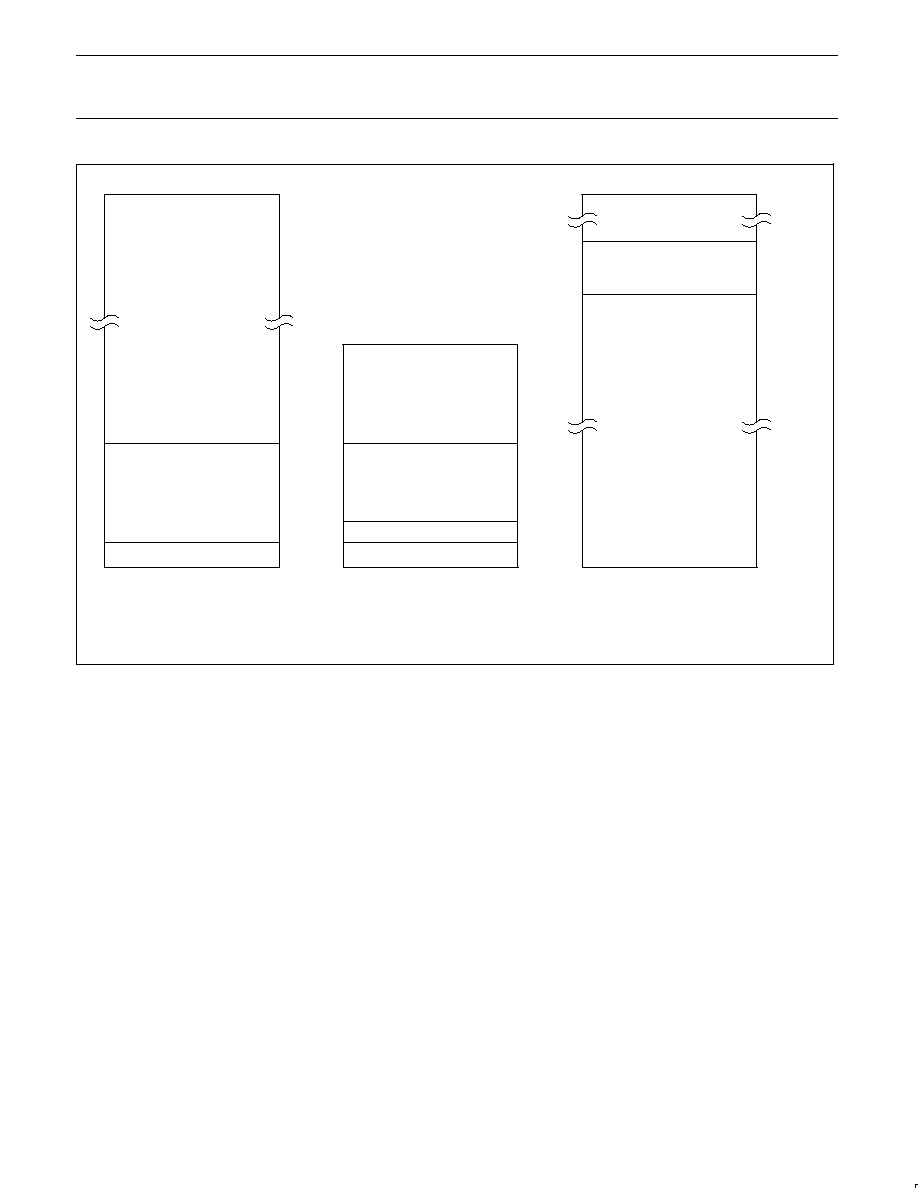
FFFFh
0400h
03FFh
FFh
80h
3Fh
0000h
00h
0000h
FD00h
FD01h
FFFFh
ON-CHIP CODE
MEMORY SPACE
ON-CHIP DATA
MEMORY SPACE
EXTERNAL DATA
MEMORY SPACE
1
1. The P87LPC759 does not support access to external data memory. However, the User Configuration Bytes are accessed via the MOVX
instruction as if they were in external data memory.
Figure 1. P87LPC759 Program and Data Memory Map

Philips Semiconductors
Preliminary data
P87LPC759
Low power, low price, low pin count (14 pin)
microcontroller with 1 kbyte OTP
2002 Mar 21
5
PIN DESCRIPTION
MNEMONIC
PIN NO.
TYPE
NAME AND FUNCTION
P0.3≠P0.6
10, 12≠14
I/O
Port 0: Port 0 is a 4-bit I/O port with a user-configurable output type. Port 0 latches are con-
figured in the quasi-bidirectional mode and have either ones or zeros written to them during
reset, as determined by the PRHI bit in the UCFG1 configuration byte. The operation of port
0 pins as inputs and outputs depends upon the port configuration selected. Each port pin is
configured independently. Refer to the section on I/O port configuration and the DC Electri-
cal Characteristics for details.
The Keyboard Interrupt feature operates with port 0 pins.
P1.0≠P1.3
P1.5, P1.7
1≠2
6≠9
I/O
Port 1: Port 1 is an 6-bit I/O port with a user-configurable output type, except for three pins
as noted below. Port 1 latches are configured in the quasi-bidirectional mode and have ei-
ther ones or zeros written to them during reset, as determined by the PRHI bit in the UCFG1
configuration byte. The operation of the configurable port 1 pins as inputs and outputs de-
pends upon the port configuration selected. Each of the configurable port pins are pro-
grammed independently. Refer to the section on I/O port configuration and the DC Electrical
Characteristics for details.
Port 1 also provides various special functions as described below.
7
I/O
O
P1.2
T0
Timer/counter 0 external count input or overflow output.
When configured as an output, P1.2 is open drain.
6
I
O
P1.3
INT0
External interrupt 0 input.
When configured as an output, P1.3 is open drain.
2
I
P1.5
RST
External Reset input (if selected via EPROM configuration). A
low on this pin resets the microcontroller, causing I/O ports and
peripherals to take on their default states, and the processor
begins execution at address 0. When used as a port pin, P1.5 is
a Schmitt trigger input only.
P2.0≠P2.1
4, 5
I/O
Port 2: Port 2 is a 2-bit I/O port with a user-configurable output type. Port 2 latches are con-
figured in the quasi-bidirectional mode and have either ones or zeros written to them during
reset, as determined by the PRHI bit in the UCFG1 configuration byte. The operation of port
2 pins as inputs and outputs depends upon the port configuration selected. Each port pin is
configured independently. Refer to the section on I/O port configuration and the DC Electri-
cal Characteristics for details.
Port 2 also provides various special functions as described below.
5
O
P2.0
X2
Output from the oscillator amplifier (when a crystal oscillator
option is selected via the EPROM configuration).
CLKOUT
CPU clock divided by 6 clock output when enabled via SFR bit
and in conjunction with internal RC oscillator or external clock
input.
4
I
P2.1
X1
Input to the oscillator circuit and internal clock generator circuits
(when selected via the EPROM configuration).
V
SS
3
I
Ground: 0 V reference.
V
DD
11
I
Power Supply: This is the power supply voltage for normal operation as well as Idle and
Power Down modes.

Philips Semiconductors
Preliminary data
P87LPC759
Low power, low price, low pin count (14 pin)
microcontroller with 1 kbyte OTP
2002 Mar 21
6
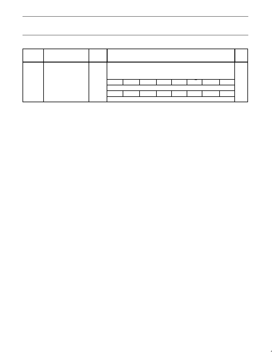
SPECIAL FUNCTION REGISTERS
Name
Description
SFR
Address
Bit Functions and Addresses
MSB
LSB
Reset
Value
E7
E6
E5
E4
E3
E2
E1
E0
ACC*
Accumulator
E0h
00h
AUXR1#
Auxiliary Function Register
A2h
KBF
BOD
BOI
LPEP
SRST
0
≠
DPS
02h
1
F7
F6
F5
F4
F3
F2
F1
F0
B*
B register
F0h
00h
DIVM#
CPU clock divide-by-M
control
95h
00h
DPTR:
Data pointer (2 bytes)
DPH
Data pointer high byte
83h
00h
DPL
Data pointer low byte
82h
00h
DF
DE
DD
DC
DB
DA
D9
D8
AF
AE
AD
AC
AB
AA
A9
A8
IEN0*
Interrupt enable 0
A8h
EA
EWD
EBO
≠
ET1
≠
ET0
EX0
00h
EF
EE
ED
EC
EB
EA
E9
E8
IEN1#*
Interrupt enable 1
E8h
≠
≠
≠
≠
≠
≠
EKB
≠
00h
1
BF
BE
BD
BC
BB
BA
B9
B8
IP0*
Interrupt priority 0
B8h
≠
PWD
PBO
≠
PT1
≠
PT0
PX0
00h
1
IP0H#
Interrupt priority 0 high
byte
B7h
≠
PWDH
PBOH
≠
PT1H
≠
PT0H
PX0H
00h
1
FF
FE
FD
FC
FB
FA
F9
F8
IP1*
Interrupt priority 1
F8h
≠
≠
≠
≠
≠
≠
PKB
≠
00h
1
IP1H#
Interrupt priority 1 high
byte
F7h
≠
≠
≠
≠
≠
≠
PKBH
≠
00h
1
KBI#
Keyboard Interrupt
86h
00h
87
86
85
84
83
82
81
80
P0*
Port 0
80h
≠
≠
≠
≠
≠
≠
≠
≠
Note 2
97
96
95
94
93
92
91
90
P1*
Port 1
90h
(P1.7)
≠
RST
≠
INT0
T0
≠
≠
Note 2
A7
A6
A5
A4
A3
A2
A1
A0
P2*
Port 2
A0h
≠
≠
≠
≠
≠
≠
X1
X2
Note 2
P0M1#
Port 0 output mode 1
84h
≠
(P0M1.6)
(P0M1.5)
(P0M1.4) (P0M1.3)
≠
≠
≠
00h
P0M2#
Port 0 output mode 2
85h
≠
(P0M2.6)
(P0M2.5)
(P0M2.4) (P0M2.3)
≠
≠
≠
00h
P1M1#
Port 1 output mode 1
91h
(P1M1.7)
≠
≠
≠
≠
≠
(P1M1.1)
(P1M1.0)
00h
1
P1M2#
Port 1 output mode 2
92h
(P1M2.7)
≠
≠
≠
≠
≠
(P1M2.1)
(P1M2.0)
00h
1
P2M1#
Port 2 output mode 1
A4h
P2S
P1S
P0S
ENCLK
≠
T0OE
(P2M1.1)
(P2M1.0)
00h
P2M2#
Port 2 output mode 2
A5h
≠
≠
≠
≠
≠
≠
(P2M2.1)
(P2M2.0)
00h
1
PCON
Power control register
87h
SMOD1
SMOD0
BOF
POF
GF1
GF0
PD
IDL
Note 3
D7
D6
D5
D4
D3
D2
D1
D0
PSW*
Program status word
D0h
CY
AC
F0
RS1
RS0
OV
F1
P
00h
SP
Stack pointer
81h
07h
8F
8E
8D
8C
8B
8A
89
88
TCON*
Timer 0 and 1 control
88h
TF1
TR1
TF0
TR0
≠
≠
IE0
IT0
00h
TH0
Timer 0 high byte
8Ch
00h
Philips Semiconductors
Preliminary data
P87LPC759
Low power, low price, low pin count (14 pin)
microcontroller with 1 kbyte OTP
2002 Mar 21
7
Name
Reset
Value
Bit Functions and Addresses
MSB
LSB
SFR
Address
Description
TH1
Timer 1 high byte
8Dh
00h
TL0
Timer 0 low byte
8Ah
00h
TL1
Timer 1 low byte
8Bh
00h
TMOD
Timer 0 and 1 mode
89h
≠
≠
M1
M0
GATE
C/T
M1
M0
00h
WDCON#
Watchdog control register
A7h
≠
≠
WDOVF
WDRUN
WDCLK
WDS2
WDS1
WDS0
Note 4
WDRST#
Watchdog reset register
A6h
XXh
NOTES:
* SFRs are bit addressable.
# SFRs are modified from or added to the 80C51 SFRs.
1. Unimplemented bits in SFRs are X (unknown) at all times. Ones should not be written to these bits since they may be used for other
purposes in future derivatives. The reset value shown in the table for these bits is 0.
2. I/O port values at reset are determined by the PRHI bit in the UCFG1 configuration byte.
3. The PCON reset value is x x BOF POF≠0 0 0 0b. The BOF and POF flags are not affected by reset. The POF flag is set by hardware upon
power up. The BOF flag is set by the occurrence of a brownout reset/interrupt and upon power up.
4. The WDCON reset value is xx11 0000b for a Watchdog reset, xx01 0000b for all other reset causes if the watchdog is enabled, and xx00
0000b for all other reset causes if the watchdog is disabled.

Philips Semiconductors
Preliminary data
P87LPC759
Low power, low price, low pin count (14 pin)
microcontroller with 1 kbyte OTP
2002 Mar 21
8
FUNCTIONAL DESCRIPTION of »-29.4398 functionse Oll be described 4 pthe f kbowing2 TD»0.00225480C51 execu0ion t
Philips Semiconductors
Preliminary data
P87LPC759
Low power, low price, low pin count (14 pin)
microcontroller with 1 kbyte OTP
2002 Mar 21
9
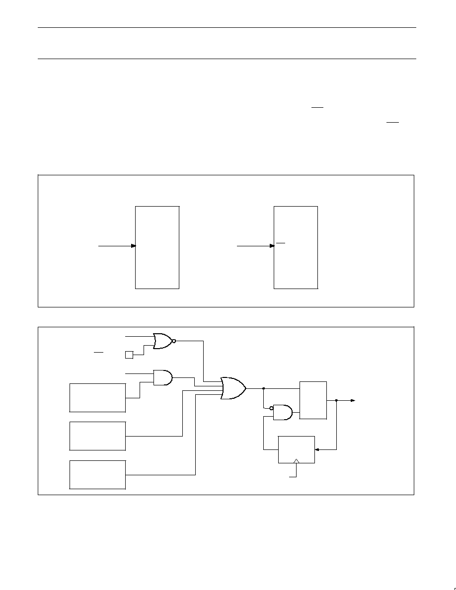
External Interrupt Inputs
The P87LPC759 has one individual interrupt input as well as the
Keyboard Interrupt function. The latter is described separately in this
section. The interrupt input is identical to those present on the
standard 80C51 microcontroller.
The external source can be programmed to be level-activated or
transition-activated by setting or clearing bit IT0 in Register TCON. If
IT0 = 0, external interrupt 0 is triggered by a detected low at the
INT0 pin. If IT0 = 1, external interrupt 0 is edge triggered. In this
mode if successive samples of the INT0 pin show a high in one
cycle and a low in the next cycle, interrupt request flag IE0 in TCON
is set, causing an interrupt request.
Since the external interrupt pin is sampled once each machine
cycle, an input high or low should hold for at least 6 CPU Clocks to
ensure proper sampling. If the external interrupt is
transition-activated, the external source has to hold the request pin
high for at least one machine cycle, and then hold it low for at least
one machine cycle. This is to ensure that the transition is detected
and that interrupt request flag IE0 is set. IE0 is automatically cleared
by the CPU when the service routine is called.
If the external interrupt is level-activated, the external source must
hold the request active until the requested interrupt is actually
generated. If the external interrupt is still asserted when the interrupt
service routine is completed another interrupt will be generated. It is
not necessary to clear the interrupt flag IE0 when the interrupt is
level sensitive, it simply tracks the input pin level.
If the external interrupt is enabled when the P87LPC759 is put into
Power Down or Idle mode, the interrupt will cause the processor to
wake up and resume operation. Refer to the section on Power
Reduction Modes for details.
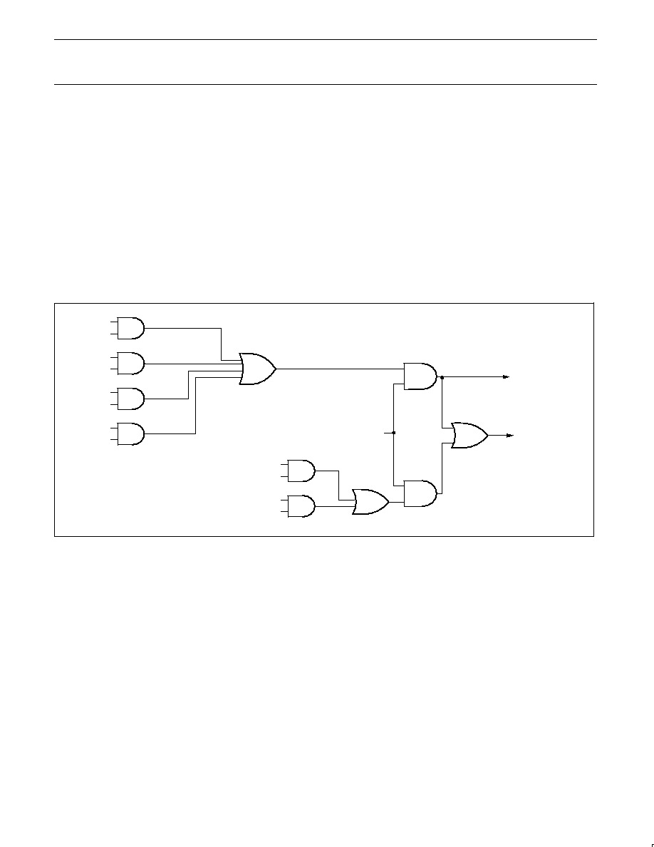
SU01644
WAKEUP
(IF IN POWER
DOWN)
EA
(FROM IEN0
REGISTER)
INTERRUPT
TO CPU
IE0
EX0
BOF
EBO
KBF
EKB
WDT
EWD
TF0
ET0
TF1
ET1
Figure 2. Interrupt Sources, Interrupt Enables, and Power Down Wakeup Sources

Philips Semiconductors
Preliminary data
P87LPC759
Low power, low price, low pin count (14 pin)
microcontroller with 1 kbyte OTP
2002 Mar 21
10
I/O Ports
The P87LPC759 has 3 I/O ports, port 0, port 1, and port 2. The
exact number of I/O pins available depend upon the oscillator and
reset options chosen. At least 9 pins of the P87LPC759 may be
used as I/Os when a two-pin external oscillator and an external
reset circuit are used. Up to 12 pins may be available if fully on-chip
oscillator and reset configurations are chosen.
All but three I/O port pins on the P87LPC759 may be software
configured to one of four types on a bit-by-bit basis, as shown in
Table 2. These are: quasi-bidirectional (standard 80C51 port
outputs), push-pull, open drain, and input only. Two configuration
registers for each port choose the output type for each port pin.
Table 2. Port Output Configuration Settings
PxM1.y
PxM2.y
Port Output Mode
0
0
Quasi-bidirectional
0
1
Push-Pull
1
0
Input Only (High Impedance)
1
1
Open Drain
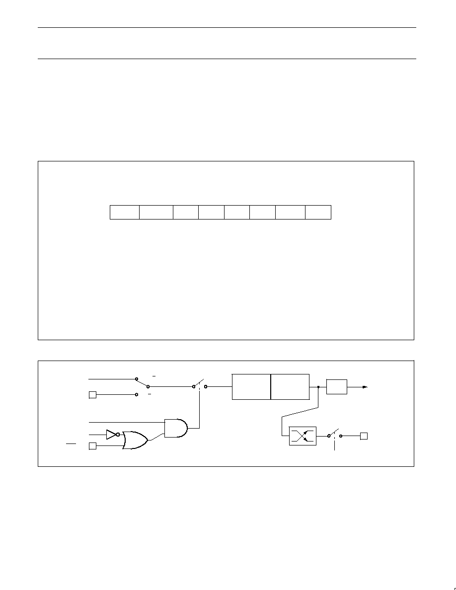
Quasi-Bidirectional Output
Configuration
The default port output configuration for standard P87LPC759 I/O
ports is the quasi-bidirectional output that is common on the 80C51
and most of its derivatives. This output type can be used as both an
input and output without the need to reconfigure the port. This is
possible because when the port outputs a logic high, it is weakly
driven, allowing an external device to pull the pin low. When the pin
is pulled low, it is driven strongly and able to sink a fairly large
current. These features are somewhat similar to an open drain
output except that there are three pull-up transistors in the
quasi-bidirectional output that serve different purposes.
One of these pull-ups, called the "very weak" pull-up, is turned on
whenever the port latch for the pin contains a logic 1. The very weak
pull-up sources a very small current that will pull the pin high if it is
left floating.
A second pull-up, called the "weak" pull-up, is turned on when the
port latch for the pin contains a logic 1 and the pin itself is also at a
logic 1 level. This pull-up provides the primary source current for a
quasi-bidirectional pin that is outputting a 1. If a pin that has a logic 1
on it is pulled low by an external device, the weak pull-up turns off,
and only the very weak pull-up remains on. In order to pull the pin
low under these conditions, the external device has to sink enough
current to overpower the weak pull-up and take the voltage on the
port pin below its input threshold.
The third pull-up is referred to as the "strong" pull-up. This pull-up is
used to speed up low-to-high transitions on a quasi-bidirectional port
pin when the port latch changes from a logic 0 to a logic 1. When
this occurs, the strong pull-up turns on for a brief time, two CPU
clocks, in order to pull the port pin high quickly. Then it turns off
again.
The quasi-bidirectional port configuration is shown in Figure 3.
SU01159
WEAK
VERY
WEAK
STRONG
PORT
PIN
V
DD
2 CPU
CLOCK DELAY
INPUT
DATA
PORT LATCH
DATA
N
P
P
P
Figure 3. Quasi-Bidirectional Output
Philips Semiconductors
Preliminary data
P87LPC759
Low power, low price, low pin count (14 pin)
microcontroller with 1 kbyte OTP
2002 Mar 21
11
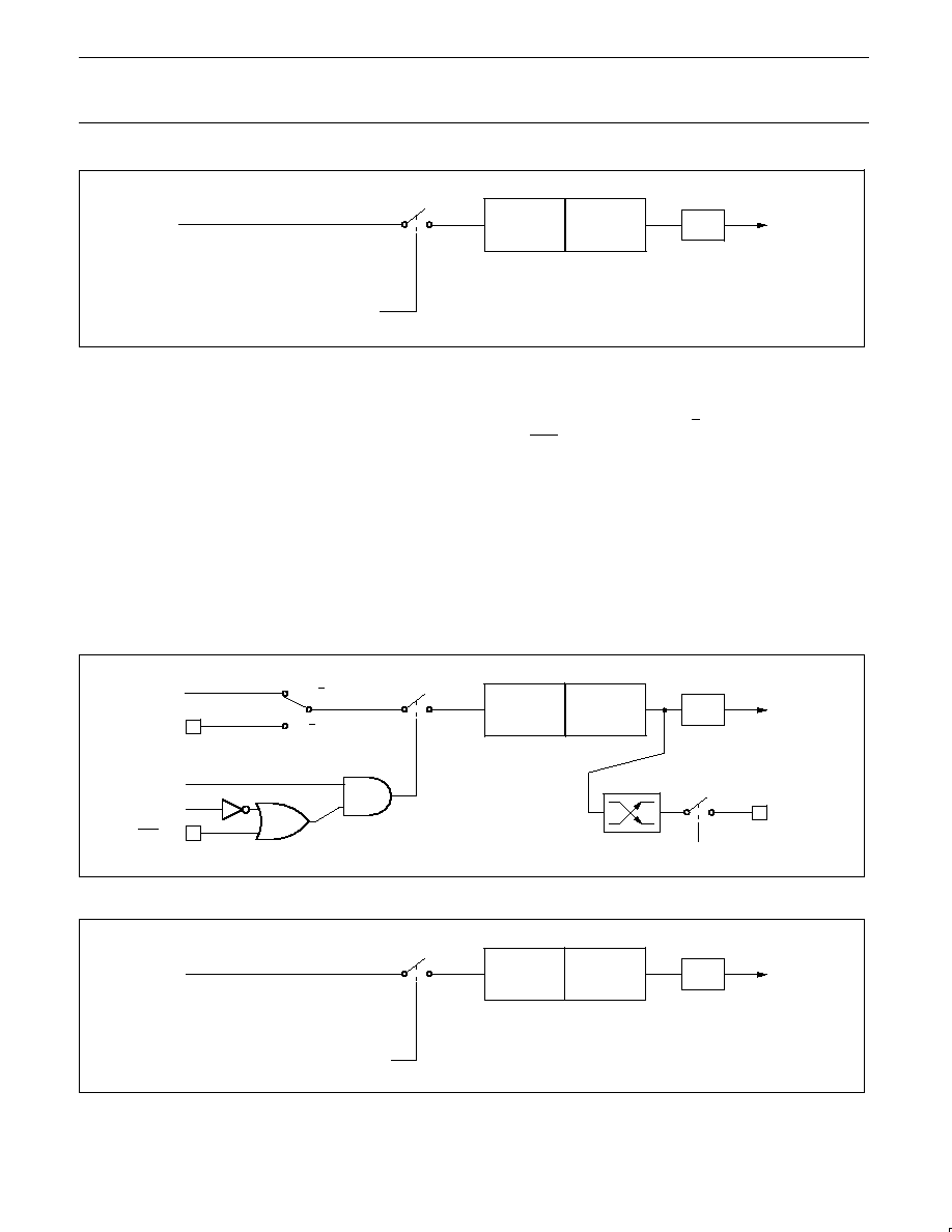
Open Drain Output
Configuration
The open drain output configuration turns off all pull-ups and only
drives the pull-down transistor of the port driver when the port latch
contains a logic 0. To be used as a logic output, a port configured in
this manner must have an external pull-up, typically a resistor tied to
V
DD
. The pull-down for this mode is the same as for the
quasi-bidirectional mode.
The open drain port configuration is shown in Figure 4.
Push-Pull Output
Configuration
The push-pull output configuration has the same pull-down structure
as both the open drain and the quasi-bidirectional output modes, but
provides a continuous strong pull-up when the port latch contains a
logic 1. The push-pull mode may be used when more source current
is needed from a port output.
The push-pull port configuration is shown in Figure 5.
The three port pins that cannot be configured are P1.2, P1.3, and
P1.5. The port pins P1.2 and P1.3 are permanently configured as
open drain outputs. They may be used as inputs by writing ones to
their respective port latches. P1.5 may be used as a Schmitt trigger
input if the P87LPC759 has been configured for an internal reset
and is not using the external reset input function RST.
Additionally, port pins P2.0 and P2.1 are disabled for both input and
output if one of the crystal oscillator options is chosen. Those
options are described in the Oscillator section.
The value of port pins at reset is determined by the PRHI bit in the
UCFG1 register. Ports may be configured to reset high or low as
needed for the application. When port pins are driven high at reset,
they are in quasi-bidirectional mode and therefore do not source
large amounts of current.
Every output on the P87LPC759 may potentially be used as a
20 mA sink LED drive output. However, there is a maximum total
output current for all ports which must not be exceeded.
All ports pins of the P87LPC759 have slew rate controlled outputs.
This is to limit noise generated by quickly switching output signals.
The slew rate is factory set to approximately 10 ns rise and fall
times.
The bits in the P2M1 register that are not used to control
configuration of P2.1 and P2.0 are used for other purposes. These
bits can enable Schmitt trigger inputs on each I/O port, enable
toggle outputs from Timer 0 and Timer 1, and enable a clock output
if either the internal RC oscillator or external clock input is being
used. The last two functions are described in the Timer/Counters
and Oscillator sections respectively. The enable bits for all of these
functions are shown in Figure 6.
Each I/O port of the P87LPC759 may be selected to use TTL level
inputs or Schmitt inputs with hysteresis. A single configuration bit
determines this selection for the entire port. Port pins P1.2, P1.3,
and P1.5 always have a Schmitt trigger input.
SU01160
PORT
PIN
INPUT
DATA
PORT LATCH
DATA
N
Figure 4. Open Drain Output
SU01161
PORT
PIN
V
DD
INPUT
DATA
PORT LATCH
DATA
N
P
Figure 5. Push-Pull Output

Philips Semiconductors
Preliminary data
P87LPC759
Low power, low price, low pin count (14 pin)
microcontroller with 1 kbyte OTP
2002 Mar 21
12
SU01535
BIT
SYMBOL
FUNCTION
P2M1.7
P2S
When P2S = 1, this bit enables Schmitt trigger inputs on Port 2.
P2M1.6
P1S
When P1S = 1, this bit enables Schmitt trigger inputs on Port 1.
P2M1.5
P0S
When P0S = 1, this bit enables Schmitt trigger inputs on Port 0.
P2M1.4
ENCLK
When ENCLK is set and the 87LPC760 is configured to use the on-chip RC oscillator, a clock
output is enabled on the X2 pin (P2.0). Refer to the Oscillator section for details.
P2M1.2
T0OE
When set, the P1.2 pin is toggled whenever Timer 0 overflows. The output frequency is therefore
one half of the Timer 0 overflow rate. Refer to the Timer/Counters section for details.
P2M1.1, P2M1.0
--
These bits, along with the matching bits in the P2M2 register, control the output configuration of
P2.1 and P2.0 respectively
1
.
(P2M1.0)
(P2M1.1)
T0OE
≠
ENCLK
P0S
P1S
P2S
0
1
2
3
4
5
6
7
P2M1
Reset Value: 00h
Not Bit Addressable
Address: A4h
1. See Table 2, Port Output Configuration Settings.
Figure 6. Port 2 Mode Register 1 (P2M1)
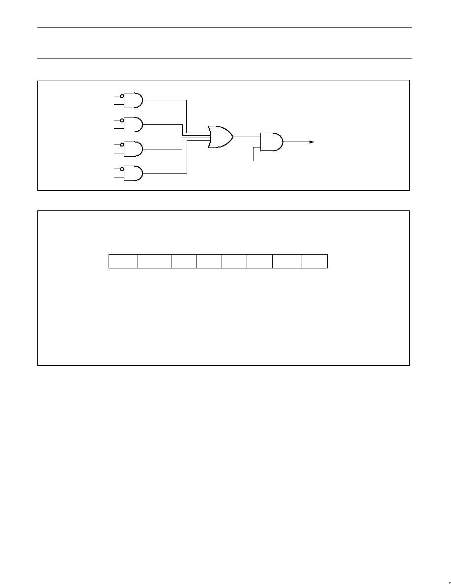
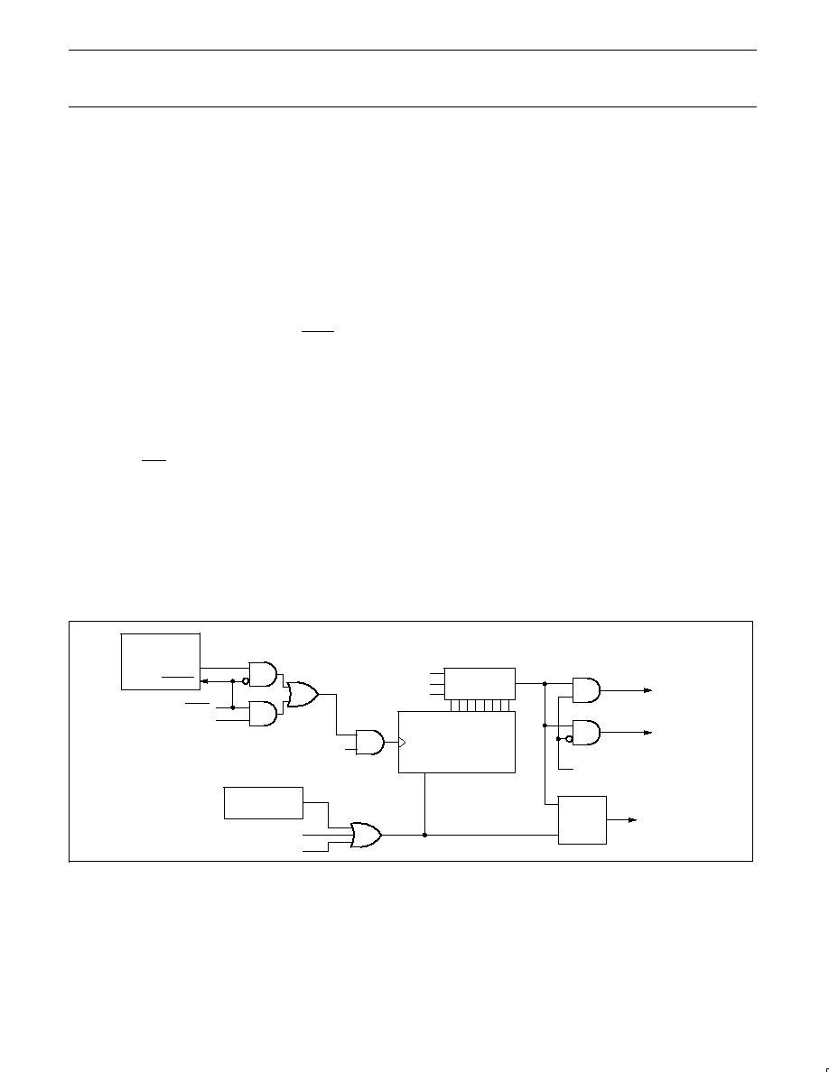
Keyboard Interrupt (KBI)
The Keyboard Interrupt function is intended primarily to allow a
single interrupt to be generated when any key is pressed on a
keyboard or keypad connected to specific pins of the P87LPC759,
as shown in Figure 7. This interrupt may be used to wake up the
CPU from Idle or Power Down modes. This feature is particularly
useful in handheld, battery powered systems that need to carefully
manage power consumption yet also need to be convenient to use.
The P87LPC759 allows any pin of port 0 to be enabled to cause this
interrupt. Port pins are enabled by the setting of bits in the KBI
register, as shown in Figure 8. The Keyboard Interrupt Flag (KBF) in
the AUXR1 register is set when any enabled pin is pulled low while
the KBI interrupt function is active. An interrupt will generated if it
has been enabled. Note that the KBF bit must be cleared by
software.
Due to human time scales and the mechanical delay associated with
keyswitch closures, the KBI feature will typically allow the interrupt
service routine to poll port 0 in order to determine which key was
pressed, even if the processor has to wake up from Power Down
mode. Refer to the section on Power Reduction Modes for details.
Philips Semiconductors
Preliminary data
P87LPC759
Low power, low price, low pin count (14 pin)
microcontroller with 1 kbyte OTP
2002 Mar 21
13
SU01536
KBF (KBI INTERRUPT)
EKB
(FROM IEN1 REGISTER)
P0.6
P0.5
P0.4
P0.3
KBI.6
KBI.5
KBI.4
KBI.3
Figure 7. Keyboard Interrupt
BIT
SYMBOL
FUNCTION
KBI.6
KBI.6
When set, enables P0.6 as a cause of a Keyboard Interrupt.
KBI.5
KBI.5
When set, enables P0.5 as a cause of a Keyboard Interrupt.
KBI.4
KBI.4
When set, enables P0.4 as a cause of a Keyboard Interrupt.
KBI.3
KBI.3
When set, enables P0.3 as a cause of a Keyboard Interrupt.
Note: the Keyboard Interrupt must be enabled in order for the settings of the KBI register to be effective. The interrupt flag
(KBF) is located at bit 7 of AUXR1.
≠
SU01537
≠
≠
KBI.3
KBI.4
KBI.5
KBI.6
≠
0
1
2
3
4
5
6
7
KBI
Reset Value: 00h
Not Bit Addressable
Address: 86h
Figure 8. Keyboard Interrupt Register (KBI)
Philips Semiconductors
Preliminary data
P87LPC759
Low power, low price, low pin count (14 pin)
microcontroller with 1 kbyte OTP
2002 Mar 21
14
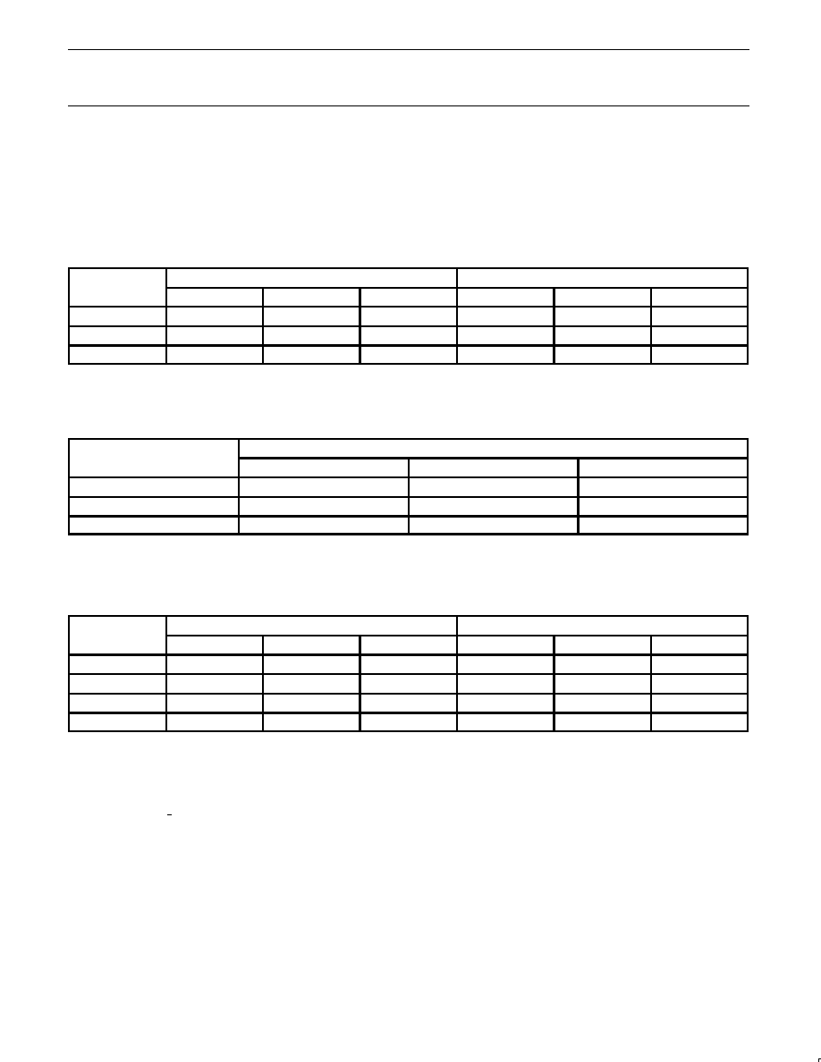
Oscillator
The P87LPC759 provides several user selectable oscillator options,
allowing optimization for a range of needs from high precision to
lowest possible cost. These are configured when the EPROM is
programmed. Basic oscillator types that are supported include: low,
medium, and high speed crystals, covering a range from 20 kHz to
20 MHz; ceramic resonators; and on-chip RC oscillator.
Low Frequency Oscillator Option
This option supports an external crystal in the range of 20 kHz to
100 kHz.
Table 3 shows capacitor values that may be used with a quartz
crystal in this mode.
Table 3. Recommended oscillator capacitors for use with the low frequency oscillator option
Oscillator
V
DD
= 2.7 to 4.5 V
V
DD
= 4.5 to 6.0 V
Frequency
Lower Limit
Optimal Value
Upper Limit
Lower Limit
Optimal Value
Upper Limit
20 kHz
15 pF
15 pF
33 pF
33 pF
33 pF
47 pF
32 kHz
15 pF
15 pF
33 pF
33 pF
33 pF
47 pF
100 kHz
15 pF
15 pF
33 pF
15 pF
15 pF
33 pF
Medium Frequency Oscillator Option
This option supports an external crystal in the range of 100 kHz to
4 MHz. Ceramic resonators are also supported in this configuration.
Table 4 shows capacitor values that may be used with a quartz
crystal in this mode.
Table 4. Recommended oscillator capacitors for use with the medium frequency oscillator option
Oscillator Freq ency
V
DD
= 2.7 to 4.5 V
Oscillator Frequency
Lower Limit
Optimal Value
Upper Limit
100 kHz
33 pF
33 pF
47 pF
1 MHz
15 pF
15 pF
33 pF
4 MHz
15 pF
15 pF
33 pF
High Frequency Oscillator Option
This option supports an external crystal in the range of 4 to 20 MHz.
Ceramic resonators are also supported in this configuration.
Table 5 shows capacitor values that may be used with a quartz
crystal in this mode.
Table 5. Recommended oscillator capacitors for use with the high frequency oscillator option
Oscillator
V
DD
= 2.7 to 4.5 V
V
DD
= 4.5 to 6.0 V
Frequency
Lower Limit
Optimal Value
Upper Limit
Lower Limit
Optimal Value
Upper Limit
4 MHz
15 pF
33 pF
47 pF
15 pF
33 pF
68 pF
8 MHz
15 pF
15 pF
33 pF
15 pF
33 pF
47 pF
16 MHz
≠
≠
≠
15 pF
15 pF
33 pF
20 MHz
≠
≠
≠
15 pF
15 pF
33 pF
On-Chip RC Oscillator Option
The on-chip RC oscillator option has a typical frequency of 6 MHz
and can be divided down for slower operation through the use of the
DIVM register. For on-chip oscillator tolerance see AC Electrical
Characteristics table. A clock output on the X2/P2.0 pin may be
enabled when the on-chip RC oscillator is used.
External Clock Input Option
In this configuration, the processor clock is input from an external
source driving the X1/P2.1 pin. The rate may be from 0 Hz up to
20 MHz when V
DD
is above 4.5 V and up to 10 MHz when V
DD
is
below 4.5 V. When the external clock input mode is used, the
X2/P2.0 pin may be used as a standard port pin. A clock output on
the X2/P2.0 pin may be enabled when the external clock input is
used.
Clock Output
The P87LPC759 supports a clock output function when either the
on-chip RC oscillator or external clock input options are selected.
This allows external devices to synchronize to the P87LPC759.
When enabled, via the ENCLK bit in the P2M1 register, the clock
output appears on the X2/CLKOUT pin whenever the on-chip
oscillator is running, including in Idle mode. The frequency of the
clock output is 1/6 of the CPU clock rate. If the clock output is not
needed in Idle mode, it may be turned off prior to entering Idle,
saving additional power. The clock output may also be enabled
when the external clock input option is selected.

Philips Semiconductors
Preliminary data
P87LPC759
Low power, low price, low pin count (14 pin)
microcontroller with 1 kbyte OTP
2002 Mar 21
15
SU01645
87LPC759
QUARTZ CRYSTAL OR
CERAMIC RESONATOR
X2
X1
THE OSCILLATOR MUST BE CONFIGURED IN ONE OF
THE FOLLOWING MODES:
≠ LOW FREQUENCY CRYSTAL
≠ MEDIUM FREQUENCY CRYSTAL
≠ HIGH FREQUENCY CRYSTAL
*
CAPACITOR VALUES MAY BE OPTIMIZED FOR
DIFFERENT OSCILLATOR FREQUENCIES (SEE TEXT)
A SERIES RESISTOR MAY BE REQUIRED IN ORDER TO
LIMIT CRYSTAL DRIVE LEVELS. THIS IS PARTICULARLY
IMPORTANT FOR LOW FREQUENCY CRYSTALS (SEE TEXT).
Figure 9. Using the Crystal Oscillator
SU01646
87LPC759
X2
X1
THE OSCILLATOR MUST BE CONFIGURED IN
THE EXTERNAL CLOCK INPUT MODE.
A CLOCK OUTPUT MAY BE OBTAINED ON
THE X2 PIN BY SETTING THE ENCLK BIT IN
THE P2M1 REGISTER.
CMOS COMPATIBLE EXTERNAL
OSCILLATOR SIGNAL
Figure 10. Using an External Clock Input
Philips Semiconductors
Preliminary data
P87LPC759
Low power, low price, low pin count (14 pin)
microcontroller with 1 kbyte OTP
2002 Mar 21
16
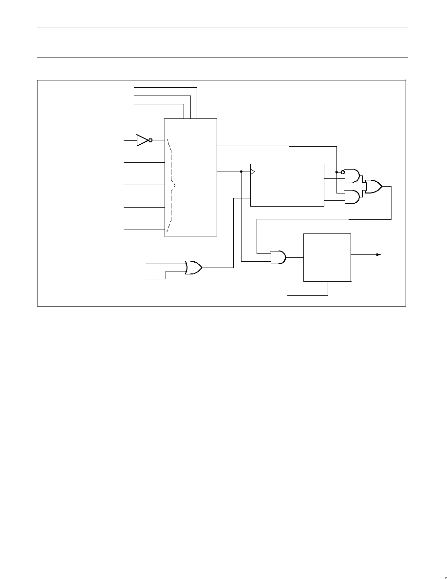
SU01167
CLOCK SELECT
CLOCK
SOURCES
CLOCK
OUT
XTAL
SELECT
INTERNAL RC OSCILLATOR
CRYSTAL: LOW FREQUENCY
CRYSTAL: MEDIUM FREQUENCY
CRYSTAL: HIGH FREQUENCY
EXTERNAL CLOCK INPUT
10-BIT RIPPLE COUNTER
RESET
COUNT
COUNT 256
COUNT 1024
OSCILLATOR STARTUP TIMER
DIVIDE-BY-M
(DIVM REGISTER)
AND
CLKR SELECT
CPU
CLOCK
˜
1/
˜
2
CLKR
(UCFG1.3)
POWER DOWN
POWER MONITOR RESET
FOSC0 (UCFG1.0)
FOSC1 (UCFG1.1)
FOSC2 (UCFG1.2)
Figure 11. Block Diagram of Oscillator Control
CPU Clock Modification: CLKR and DIVM
For backward compatibility, the CLKR configuration bit allows setting
the P87LPC759 instruction and peripheral timing to match standard
80C51 timing by dividing the CPU clock by two. Default timing for
the P87LPC759 is 6 CPU clocks per machine cycle while standard
80C51 timing is 12 clocks per machine cycle. This division also
applies to peripheral timing, allowing 80C51 code that is oscillator
frequency and/or timer rate dependent. The CLKR bit is located in
the EPROM configuration register UCFG1, described under EPROM
Characteristics
In addition to this, the CPU clock may be divided down from the
oscillator rate by a programmable divider, under program control.
This function is controlled by the DIVM register. If the DIVM register
is set to zero (the default value), the CPU will be clocked by either
the unmodified oscillator rate, or that rate divided by two, as
determined by the previously described CLKR function.
When the DIVM register is set to some value N (between 1 and
255), the CPU clock is divided by 2 * (N + 1). Clock division values
from 4 through 512 are thus possible. This feature makes it possible
to temporarily run the CPU at a lower rate, reducing power
consumption, in a manner similar to Idle mode. By dividing the clock,
the CPU can retain the ability to respond to events other than those
that can cause interrupts (i.e. events that allow exiting the Idle
mode) by executing its normal program at a lower rate. This can
allow bypassing the oscillator startup time in cases where Power
Down mode would otherwise be used. The value of DIVM may be
changed by the program at any time without interrupting code
execution.
Power Monitoring Functions
The P87LPC759 incorporates power monitoring functions designed
to prevent incorrect operation during initial power up and power loss
or reduction during operation. This is accomplished with two
hardware functions: Power-On Detect and Brownout Detect.
Brownout Detection
The Brownout Detect function allows preventing the processor from
failing in an unpredictable manner if the power supply voltage drops
below a certain level. The default operation is for a brownout
detection to cause a processor reset, however it may alternatively
be configured to generate an interrupt by setting the BOI bit in the
AUXR1 register (AUXR1.5).
The P87LPC759 allows selection of two Brownout levels: 2.5 V or
3.8 V. When V
DD
drops below the selected voltage, the brownout
detector triggers and remains active until V
DD
is returns to a level
above the Brownout Detect voltage. When Brownout Detect causes
a processor reset, that reset remains active as long as V
DD
remains
below the Brownout Detect voltage. When Brownout Detect
generates an interrupt, that interrupt occurs once as V
DD
crosses
from above to below the Brownout Detect voltage. For the interrupt
to be processed, the interrupt system and the BOI interrupt must
both be enabled (via the EA and EBO bits in IEN0).
When Brownout Detect is activated, the BOF flag in the PCON
register is set so that the cause of processor reset may be
determined by software. This flag will remain set until cleared by
software.

Philips Semiconductors
Preliminary data
P87LPC759
Low power, low price, low pin count (14 pin)
microcontroller with 1 kbyte OTP
2002 Mar 21
17
For correct activation of Brownout Detect, the V
DD
fall time must be
no faster than 50 mV/
µ
s. When V
DD
is restored, is should not rise
faster than 2 mV/
µ
s in order to insure a proper reset.
The brownout voltage (2.5 V or 3.8 V) is selected via the BOV bit in
the EPROM configuration register UCFG1. When unprogrammed
(BOV = 1), the brownout detect voltage is 2.5 V. When programmed
(BOV = 0), the brownout detect voltage is 3.8 V.
If the Brownout Detect function is not required in an application, it
may be disabled, thus saving power. Brownout Detect is disabled by
setting the control bit BOD in the AUXR1 register (AUXR1.6).
Power On Detection
The Power On Detect has a function similar to the Brownout Detect,
but is designed to work as power comes up initially, before the
power supply voltage reaches a level where Brownout Detect can
work. When this feature is activated, the POF flag in the PCON
register is set to indicate an initial power up condition. The POF flag
will remain set until cleared by software.
Power Reduction Modes
The P87LPC759 supports Idle and Power Down modes of power
reduction.
Idle Mode
The Idle mode leaves peripherals running in order to allow them to
activate the processor when an interrupt is generated. Any enabled
interrupt source or Reset may terminate Idle mode. Idle mode is
entered by setting the IDL bit in the PCON register (see Figure 12).
Power Down Mode
The Power Down mode stops the oscillator in order to absolutely
minimize power consumption. Power Down mode is entered by
setting the PD bit in the PCON register (see Figure 12).
The processor can be made to exit Power Down mode via Reset or
one of the interrupt sources shown in Table 3. This will occur if the
interrupt is enabled and its priority is higher than any interrupt
currently in progress.
In Power Down mode, the power supply voltage may be reduced to
the RAM keep-alive voltage V
RAM
. This retains the RAM contents at
the point where Power Down mode was entered. SFR contents are
not guaranteed after V
DD
has been lowered to V
RAM
, therefore it is
recommended to wake up the processor via Reset in this case. V
DD
must be raised to within the operating range before the Power Down
mode is exited. Since the watchdog timer has a separate oscillator, it
may reset the processor upon overflow if it is running during Power
Down.
Note that if the Brownout Detect reset is enabled, the processor will
be put into reset as soon as V
DD
drops below the brownout voltage.
If Brownout Detect is configured as an interrupt and is enabled, it will
wake up the processor from Power Down mode when V
DD
drops
below the brownout voltage.
When the processor wakes up from Power Down mode, it will start
the oscillator immediately and begin execution when the oscillator is
stable. Oscillator stability is determined by counting 1024 CPU
clocks after start-up when one of the crystal oscillator configurations
is used, or 256 clocks after start-up for the internal RC or external
clock input configurations.
Some chip functions continue to operate and draw power during
Power Down mode, increasing the total power used during Power
Down. These include the Brownout Detect and Watchdog Timer.
BIT
SYMBOL
FUNCTION
PCON.7
≠
Reserved
PCON.6
≠
Reserved
PCON.5
BOF
Brown Out Flag. Set automatically when a brownout reset or interrupt has occurred. Also set at
power on. Cleared by software. Refer to the Power Monitoring Functions section for additional
information.
PCON.4
POF
Power On Flag. Set automatically when a power-on reset has occurred. Cleared by software. Refer
to the Power Monitoring Functions section for additional information.
PCON.3
GF1
General purpose flag 1. May be read or written by user software, but has no effect on operation.
PCON.2
GF0
General purpose flag 0. May be read or written by user software, but has no effect on operation.
PCON.1
PD
Power Down control bit. Setting this bit activates Power Down mode operation. Cleared when the
Power Down mode is terminated (see text).
PCON.0
IDL
Idle mode control bit. Setting this bit activates Idle mode operation. Cleared when the Idle mode is
terminated (see text).
IDL
SU01647
PD
GF0
GF1
POF
BOF
≠
≠
0
1
2
3
4
5
6
7
PCON
Reset Value:
S
30h for a Power On reset
S
20h for a Brownout reset
S
00h for other reset sources
Not Bit Addressable
Address: 87h
Figure 12. Power Control Register (PCON)
Philips Semiconductors
Preliminary data
P87LPC759
Low power, low price, low pin count (14 pin)
microcontroller with 1 kbyte OTP
2002 Mar 21
18
Table 6. Sources of Wakeup from Power Down Mode
Wakeup Source
Conditions
External Interrupt 0
The interrupt must be enabled.
Keyboard Interrupt
The keyboard interrupt feature must be enabled and properly set up. The corresponding interrupt must be
enabled.
Watchdog Timer Reset
The watchdog timer must be enabled via the WDTE bit in the UCFG1 EPROM configuration byte.
Watchdog Timer Interrupt
The WDTE bit in the UCFG1 EPROM configuration byte must not be set. The corresponding interrupt must
be enabled.
Brownout Detect Reset
The BOD bit in AUXR1 must not be set (brownout detect not disabled). The BOI bit in AUXR1 must not be
set (brownout interrupt disabled).
Brownout Detect Interrupt
The BOD bit in AUXR1 must not be set (brownout detect not disabled). The BOI bit in AUXR1 must be set
(brownout interrupt enabled). The corresponding interrupt must be enabled.
Reset Input
The external reset input must be enabled.
Philips Semiconductors
Preliminary data
P87LPC759
Low power, low price, low pin count (14 pin)
microcontroller with 1 kbyte OTP
2002 Mar 21
19
Low Voltage EPROM Operation
The EPROM array contains some analog circuits that are not
required when V
DD
is less than 4 V, but are required for a V
DD
greater than 4 V. The LPEP bit (AUXR.4), when set by software, will
power down these analog circuits resulting in a reduced supply
current. LPEP is cleared only by power-on reset, so it may be set
ONLY for applications that always operate with V
DD
less than 4 V.
Reset
The P87LPC759 has an integrated power-on reset circuit which
always provides a reset when power is initially applied to the device.
It is recommended to use the internal reset whenever possible to
save external components and to be able to use pin P1.5 as a
general-purpose input pin.
The P87LPC759 can additionally be configured to use P1.5 as an
external active-low reset pin RST by programming the RPD bit in the
User Configuration Register UCFG1 to 0. The internal reset is still
active on power-up of the device. While the signal on the RST pin is
low, the P87LPC759 is held in reset until the signal goes high.
The watchdog timer on the P87LPC759 can act as an oscillator fail
detect because it uses an independent, fully on-chip oscillator.
UCFG1 is described in the System Configuration Bytes section of
this datasheet.
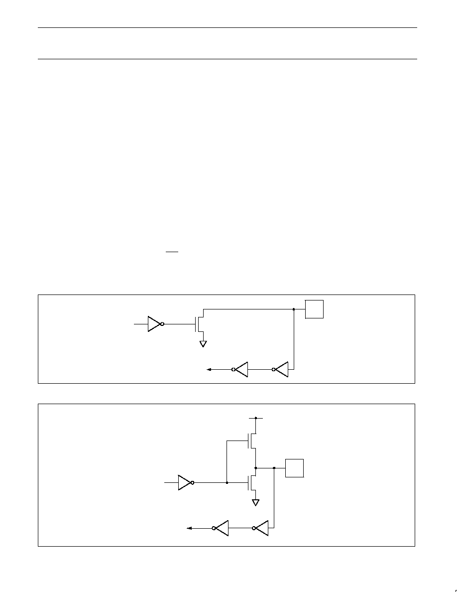
SU01648
P87LPC759
P1.5
Pin is used as
digital input pin
Internal power-on
Reset active
UCFG1.RPD = 1 (default)
P87LPC759
RST
Pin is used as
active-low reset pin
Internal power-on
Reset active
UCFG1.RPD = 0
Figure 13. Using pin P1.5 as general purpose input pin or as low-active reset pin
SU01170
CHIP RESET
CPU
CLOCK
Q
RESET
TIMING
RPD (UCFG1.6)
WDT
MODULE
SOFTWARE RESET
SRST (AUXR1.3)
POWER MONITOR
RESET
RST/V
PP
PIN
WDTE (UCFG1.7)
S
R
Figure 14. Block Diagram Showing Reset Sources

Philips Semiconductors
Preliminary data
P87LPC759
Low power, low price, low pin count (14 pin)
microcontroller with 1 kbyte OTP
2002 Mar 21
20
Timer/Counters
The P87LPC759 has two general purpose counter/timers which are
upward compatible with the standard 80C51 Timer 0 and Timer 1.
Both can be configured to operate as timers or can be configured to
be an event counter (see Figure 15). An option to automatically
toggle the T0 pin upon timer overflow has been added.
In the "Timer" function, the register is incremented every machine
cycle. Thus, one can think of it as counting machine cycles. Since a
machine cycle consists of 6 CPU clock periods, the count rate is 1/6
of the CPU clock frequency. Refer to the section Enhanced CPU for
a description of the CPU clock.
In the "Counter" function of Timer 0, the register is incremented in
response to a 1-to-0 transition at its corresponding external input
pin, T0. In this function, the external input is sampled once during
every machine cycle. When the samples of the pin state show a
high in one cycle and a low in the next cycle, the count is
incremented. The new count value appears in the register during the
cycle following the one in which the transition was detected. Since it
takes 2 machine cycles (12 CPU clocks) to recognize a 1-to-0
transition, the maximum count rate is 1/6 of the CPU clock
frequency. There are no restrictions on the duty cycle of the external
input signal, but to ensure that a given level is sampled at least once
before it changes, it should be held for at least one full machine
cycle.
The "Timer" or "Counter" function of Timer 0 is selected by control bit
C/T in the Special Function Register TMOD. In addition to the
"Timer" or "Counter" selection, Timer 0 and Timer 1 have four
operating modes, which are selected by bit-pairs (M1, M0) in TMOD.
Modes 0, 1, and 2 are the same for both Timers/Counters. Mode 3 is
different. The four operating modes are described in the following
text.
BIT
SYMBOL
FUNCTION
TMOD.7, 6
≠
Reserved. Must be written with zeros only.
TMOD.5, 4
M1, M0
Mode Select for Timer 1 (see table below).
TMOD.3
GATE
Gating control for Timer 0. When set, Timer/Counter is enabled only while the INT0 pin is high and
the TR0 control pin is set. When cleared, Timer 0 is enabled when the TR0 control bit is set.
TMOD.2
C/T
Timer or Counter Selector for Timer 0. Cleared for Timer operation (input from internal system clock.)
Set for Counter operation (input from T0 input pin).
TMOD.1, 0
M1, M0
Mode Select for Timer 0 (see table below).
M1, M0
Timer Mode
0 0
8048 Timer "TLn" serves as 5-bit prescaler.
0 1
16-bit Timer/Counter "THn" and "TLn" are cascaded; there is no prescaler.
1 0
8-bit auto-reload Timer/Counter. THn holds a value which is loaded into TLn when it overflows.
1 1
Timer 0 is a dual 8-bit Timer/Counter in this mode. TL0 is an 8-bit Timer/Counter controlled by the
standard Timer 0 control bits. TH0 is an 8-bit timer only, controlled by the Timer 1 control bits (see
text). Timer 1 in this mode is stopped.
M0
SU01542
M1
C/T
GATE
M0
M1
≠
≠
0
1
2
3
4
5
6
7
TMOD
Reset Value: 00h
Not Bit Addressable
Address: 89h
T1
T0
Figure 15. Timer/Counter Mode Control Register (TMOD)
Philips Semiconductors
Preliminary data
P87LPC759
Low power, low price, low pin count (14 pin)
microcontroller with 1 kbyte OTP
2002 Mar 21
21
Mode 0
Putting either Timer into Mode 0 makes it look like an 8048 Timer,
which is an 8-bit Counter with a divide-by-32 prescaler. Figures 17
and 18 show Mode 0 operation.
In this mode, the Timer register is configured as a 13-bit register. As
the count rolls over from all 1s to all 0s, it sets the Timer interrupt
flag TFn. The count input is enabled to Timer 0 when TR0 = 1 and
either GATE = 0 or INT0 = 1. (Setting GATE = 1 allows the Timer to
be controlled by external input INT0, to facilitate pulse width
measurements). TRn is a control bit in the Special Function Register
TCON (Figure 16). The GATE bit is in the TMOD register (TMOD.3).
The 13-bit register consists of all 8 bits of THn and the lower 5 bits
of TLn. The upper 3 bits of TLn are indeterminate and should be
ignored. Setting the run flag (TRn) does not clear the registers.
Mode 0 operation is slightly different for Timer 0 and Timer 1. See
Figures 17 and 18.
BIT
SYMBOL
FUNCTION
TCON.7
TF1
Timer 1 overflow flag. Set by hardware on Timer/Counter overflow. Cleared by hardware when the
interrupt is processed, or by software.
TCON.6
TR1
Timer 1 Run control bit. Set/cleared by software to turn Timer/Counter 1 on/off.
TCON.5
TF0
Timer 0 overflow flag. Set by hardware on Timer/Counter overflow. Cleared by hardware when the
processor vectors to the interrupt routine, or by software.
TCON.4
TR0
Timer 0 Run control bit. Set/cleared by software to turn Timer/Counter 0 on/off.
TCON.3, 2
≠
Reserved (must be 0).
TCON.1
IE0
Interrupt 0 Edge flag. Set by hardware when external interrupt 0 edge is detected. Cleared by
hardware when the interrupt is processed, or by software.
TCON.0
IT0
Interrupt 0 Type control bit. Set/cleared by software to specify falling edge/low level triggered
external interrupts.
IT0
SU01543
IE0
≠
≠
TR0
TF0
TR1
TF1
0
1
2
3
4
5
6
7
TCON
Reset Value: 00h
Bit Addressable
Address: 88h
Figure 16. Timer/Counter Control Register (TCON)
SU01544
TL0
(5 BITS)
TH0
(8 BITS)
OSC/6 OR
OSC/12
OVERFLOW
T0 PIN
T0OE
TOGGLE
CONTROL
C/T = 1
C/T = 0
T0 PIN
TR0
GATE
INT0 PIN
INTERRUPT
TF0
Figure 17. Timer/Counter 0 in Mode 0 (13-Bit Timer/Counter)
Philips Semiconductors
Preliminary data
P87LPC759
Low power, low price, low pin count (14 pin)
microcontroller with 1 kbyte OTP
2002 Mar 21
22
SU01553
TL1
(5 BITS)
TH1
(8 BITS)
OSC/6 OR
OSC/12
OVERFLOW
CONTROL
TR1
INTERRUPT
TF1
Figure 18. Timer 1 in Mode 0 (13-Bit Timer)
Mode 1
Mode 1 is the same as Mode 0, except that all 16 bits of the timer
register (THn and TLn) are used. (See Figures 19 and 20)
Mode 2
Mode 2 configures the Timer register as an 8-bit Counter (TLn) with
automatic reload, as shown in Figures 21 and 22. Overflow from TLn
not only sets TFn, but also reloads TLn with the contents of THn,
which must be preset by software. The reload leaves THn
unchanged. Mode 2 operation is slightly different for Timer 0 and
Timer 1 (see Figures 21 and 22).
Mode 3
When Timer 1 is in Mode 3 it is stopped. The effect is the same as
setting TR1 = 0.
Timer 0 in Mode 3 establishes TL0 and TH0 as two separate 8-bit
counters. The logic for Mode 3 on Timer 0 is shown in Figure 23.
TL0 uses the Timer 0 control bits: C/T, GATE, TR0, and TF0 as well
as the INT0 pin. TH0 is locked into a timer function (counting
machine cycles) and takes over the use of TR1 and TF1 from Timer
1. Thus, TH0 now controls the "Timer 1" interrupt.
Mode 3 is provided for applications that require an extra 8-bit timer.
With Timer 0 in Mode 3, an P87LPC759 can look like it has three
Timer/Counters. When Timer 0 is in Mode 3, Timer 1 can be turned
on and off by switching it into and out of its own Mode 3. It can still
be used by the serial port as a baud rate generator, or in any
application not requiring an interrupt.
SU01545
TL0
(8 BITS)
TH0
(8 BITS)
OSC/6 OR
OSC/12
OVERFLOW
T0 PIN
T0OE
TOGGLE
CONTROL
C/T = 1
C/T = 0
T0 PIN
TR0
GATE
INT0 PIN
INTERRUPT
TF0
Figure 19. Timer/Counter 0 in Mode 1 (16-Bit Timer/Counter)
SU01546
TL1
(8 BITS)
OSC/6 OR
OSC/12
OVERFLOW
CONTROL
TR1
INTERRUPT
TF1
TH1
(8 BITS)
Figure 20. Timer 1 in Mode 1 (16-Bit Timer)

Philips Semiconductors
Preliminary data
P87LPC759
Low power, low price, low pin count (14 pin)
microcontroller with 1 kbyte OTP
2002 Mar 21
23
SU01547
TL0
(8 BITS)
TH0
(8 BITS)
OSC/6 OR
OSC/12
OVERFLOW
T0 PIN
T0OE
TOGGLE
CONTROL
C/T = 1
C/T = 0
T0 PIN
TR0
GATE
INT0 PIN
INTERRUPT
TF0
RELOAD
Figure 21. Timer/Counter 0 in Mode 2 (8-Bit Auto-Reload)
SU01548
TL1
(8 BITS)
TH1
(8 BITS)
OSC/6 OR
OSC/12
OVERFLOW
CONTROL
TR1
INTERRUPT
TF1
RELOAD
Figure 22. Timer 1 in Mode 2 (8-Bit Auto-Reload)
SU01549
TL0
(8 BITS)
OSC/6 OR
OSC/12
OVERFLOW
T0 PIN
T0OE
TOGGLE
CONTROL
C/T = 1
C/T = 0
T0 PIN
TR0
GATE
INT0 PIN
INTERRUPT
TF0
TH0
(8 BITS)
OVERFLOW
CONTROL
INTERRUPT
TF1
TR1
OSC/6 OR
OSC/12
Figure 23. Timer/Counter 0 Mode 3 (Two 8-Bit Timer/Counters)
Philips Semiconductors
Preliminary data
P87LPC759
Low power, low price, low pin count (14 pin)
microcontroller with 1 kbyte OTP
2002 Mar 21
24
Timer Overflow Toggle Output
Timer 0 can be configured to automatically toggle a port output
whenever a timer overflow occurs. The same device pins that is
used for the T0 count inputs are also used for the timer toggle
outputs. This function is enabled by control bit T0OE in the P2M1
register. The port outputs will be a logic 1 prior to the first timer
overflow when this mode is turned on.
Watchdog Timer
When enabled via the WDTE configuration bit, the watchdog timer is
operated from an independent, fully on-chip oscillator in order to
provide the greatest possible dependability. When the watchdog
feature is enabled, the timer must be fed regularly by software in
order to prevent it from resetting the CPU, and it cannot be turned
off. When disabled as a watchdog timer (via the WDTE bit in the
UCFG1 configuration register), it may be used as an interval timer
and may generate an interrupt. The watchdog timer is shown in
Figure 24.
The watchdog timeout time is selectable from one of eight values,
nominal times range from 25 milliseconds to 3.2 seconds. The
frequency tolerance of the independent watchdog RC oscillator is
±
37%. When the watchdog function is enabled, the WDCON register
may be written once during chip initialization in order to set the
watchdog timeout time. The recommended method of initializing the
WDCON register is to first feed the watchdog, then write to WDCON
to configure the WDS2≠0 bits. Using this method, the watchdog
initialization may be done any time within 10 milliseconds after
startup without a watchdog overflow occurring before the
initialization can be completed.
Since the watchdog timer oscillator is fully on-chip and independent
of any external oscillator circuit used by the CPU, it intrinsically
serves as an oscillator fail detection function. If the watchdog feature
is enabled and the CPU oscillator fails for any reason, the watchdog
timer will time out and reset the CPU.
When the watchdog function is enabled, the timer is deactivated
temporarily when a chip reset occurs from another source, such as
a power on reset, brownout reset, or external reset.
Watchdog Feed Sequence
If the watchdog timer is running, it must be fed before it times out in
order to prevent a chip reset from occurring. The watchdog feed
sequence consists of first writing the value 1Eh, then the value E1h
to the WDRST register. An example of a watchdog feed sequence is
shown below.
WDFeed:
mov
WDRST,#1eh
; First part of watchdog feed
sequence.
mov
WDRST,#0e1h ; Second part of watchdog feed
sequence.
The two writes to WDRST do not have to occur in consecutive
instructions. An incorrect watchdog feed sequence does not cause
any immediate response from the watchdog timer, which will still
time out at the originally scheduled time if a correct feed sequence
does not occur prior to that time.
After a chip reset, the user program has a limited time in which to
either feed the watchdog timer or change the timeout period. When
a low CPU clock frequency is used in the application, the number of
instructions that can be executed before the watchdog overflows
may be quite small.
Watchdog Reset
If a watchdog reset occurs, the internal reset is active for
approximately one microsecond. If the CPU clock was still running,
code execution will begin immediately after that. If the processor
was in Power Down mode, the watchdog reset will start the
oscillator and code execution will resume after the oscillator is
stable.
SU01633
WATCHDOG
INTERRUPT
S
Q
20-BIT COUNTER
STATE CLOCK
WDTE (UCFG1.7)
BOF (PCON.5)
POF (PCON.4)
WATCHDOG
RESET
CLEAR
8 MSBs
8 TO 1 MUX
WATCHDOG
FEED DETECT
WDOVF
(WDCON.5)
WDS2≠0
(WDCON.2≠0)
WDTE + WDRUN
WDCLK * WDTE
500 kHz
RC OSCILLATOR
ENABLE
CLOCK OUT
R
Figure 24. Block Diagram of the Watchdog Timer

Philips Semiconductors
Preliminary data
P87LPC759
Low power, low price, low pin count (14 pin)
microcontroller with 1 kbyte OTP
2002 Mar 21
25
BIT
SYMBOL
FUNCTION
WDCON.7, 6
--
Reserved for future use. Should not be set to 1 by user programs.
WDCON.5
WDOVF
Watchdog timer overflow flag. Set when a watchdog reset or timer overflow occurs. Cleared when
the watchdog is fed.
WDCON.4
WDRUN
Watchdog run control. The watchdog timer is started when WDRUN = 1 and stopped when
WDRUN = 0. This bit is forced to 1 (watchdog running) if the WDTE configuration bit = 1.
WDCON.3
WDCLK
Watchdog clock select. The watchdog timer is clocked by CPU clock/6 when WDCLK = 1 and by
the watchdog RC oscillator when WDCLK = 0. This bit is forced to 0 (using the watchdog RC
oscillator) if the WDTE configuration bit = 1.
WDCON.2≠0 WDS2≠0
Watchdog rate select.
WDS2≠0
Timeout Clocks
Minimum Time
Nominal Time
Maximum Time
0 0 0
8,192
10 ms
16 ms
23 ms
0 0 1
16,384
20 ms
32 ms
45 ms
0 1 0
32,768
41 ms
65 ms
90 ms
0 1 1
65,536
82 ms
131 ms
180 ms
1 0 0
131,072
165 ms
262 ms
360 ms
1 0 1
262,144
330 ms
524 ms
719 ms
1 1 0
524,288
660 ms
1.05 sec
1.44 sec
1 1 1
1,048,576
1.3 sec
2.1 sec
2.9 sec
WDS0
SU01634
WDS1
WDS2
WDCLK
WDRUN
WDOVF
--
--
0
1
2
3
4
5
6
7
WDCON
Reset Value:
S
30h for a watchdog reset.
S
10h for other rest sources if the watchdog is enabled via the WDTE configuration bit.
S
00h for other reset sources if the watchdog is disabled via the WDTE configuration bit.
Not Bit Addressable
Address: A7h
Figure 25. Watchdog Timer Control Register (WDCON)

Philips Semiconductors
Preliminary data
P87LPC759
Low power, low price, low pin count (14 pin)
microcontroller with 1 kbyte OTP
2002 Mar 21
26
Additional Features
The AUXR1 register contains several special purpose control bits
that relate to several chip features. AUXR1 is described in
Figure 26.
Software Reset
The SRST bit in AUXR1 allows software the opportunity to reset the
processor completely, as if an external reset or watchdog reset had
occurred. If a value is written to AUXR1 that contains a 1 at bit
position 3, all SFRs will be initialized and execution will resume at
program address 0000. Care should be taken when writing to
AUXR1 to avoid accidental software resets.
Dual Data Pointers
The dual Data Pointer (DPTR) adds to the ways in which the
processor can specify the address used with certain instructions.
The DPS bit in the AUXR1 register selects one of the two Data
Pointers. The DPTR that is not currently selected is not accessible
to software unless the DPS bit is toggled.
Specific instructions affected by the Data Pointer selection are:
∑
INC
DPTR
Increments the Data Pointer by 1.
∑
JMP
@A+DPTR
Jump indirect relative to DPTR value.
∑
MOV
DPTR, #data16
Load the Data Pointer with a 16-bit
constant.
∑
MOVC A, @A+DPTR
Move code byte relative to DPTR to the
accumulator.
∑
MOVX A, @DPTR
Move data byte the accumulator to data
memory relative to DPTR.
∑
MOVX @DPTR, A
Move data byte from data memory
relative to DPTR to the accumulator.
Also, any instruction that reads or manipulates the DPH and DPL
registers (the upper and lower bytes of the current DPTR) will be
affected by the setting of DPS. The MOVX instructions have limited
application for the P87LPC759 since the part does not have an
external data bus. However, they may be used to access EPROM
configuration information (see EPROM Characteristics section).
Bit 2 of AUXR1 is permanently wired as a logic 0. This is so that the
DPS bit may be toggled (thereby switching Data Pointers) simply by
incrementing the AUXR1 register, without the possibility of
inadvertently altering other bits in the register.
SU01551
BIT
SYMBOL
FUNCTION
AUXR1.7
KBF
Keyboard Interrupt Flag. Set when any pin of port 0 that is enabled for the Keyboard Interrupt
function goes low. Must be cleared by software.
AUXR1.6
BOD
Brown Out Disable. When set, turns off brownout detection and saves power. See Power
Monitoring Functions section for details.
AUXR1.5
BOI
Brown Out Interrupt. When set, prevents brownout detection from causing a chip reset and allows
the brownout detect function to be used as an interrupt. See the Power Monitoring Functions
section for details.
AUXR1.4
LPEP
Low Power EPROM control bit. Allows power savings in low voltage systems. Set by software. Can
only be cleared by power-on or brownout reset. See the Power Reduction Modes section for details.
AUXR1.3
SRST
Software Reset. When set by software, resets the 87LPC760 as if a hardware reset occurred.
AUXR1.2
--
This bit contains a hard-wired 0. Allows toggling of the DPS bit by incrementing AUXR1, without
interfering with other bits in the register.
AUXR1.1
--
Reserved for future use. Should not be set to 1 by user programs.
AUXR1.0
DPS
Data Pointer Select. Chooses one of two Data Pointers for use by the program. See text for details.
DPS
--
0
SRST
LPEP
BOI
BOD
KBF
0
1
2
3
4
5
6
7
AUXR1
Reset Value: 00h
Not Bit Addressable
Address: A2h
Figure 26. AUXR1 Register

Philips Semiconductors
Preliminary data
P87LPC759
Low power, low price, low pin count (14 pin)
microcontroller with 1 kbyte OTP
2002 Mar 21
27
EPROM Characteristics
Programming of the EPROM on the P87LPC759 is accomplished
with a serial programming method. Commands, addresses, and data
are transmitted to and from the device on two pins after
programming mode is entered. Serial programming allows easy
implementation of On-Board Programming of the P87LPC759 in an
application board. Details of On-Board Programming can be found in
application note AN466.
The P87LPC759 contains three signature bytes that can be read
and used by an EPROM programming system to identify the device.
The signature bytes designate the device as an P87LPC759
manufactured by Philips. The signature bytes may be read by the
user program at addresses FC30h, FC31h and FC60h with the
MOVC instruction, using the DPTR register for addressing.
System Configuration Bytes
A number of user configurable features of the P87LPC759 must be
defined at power up and therefore cannot be set by the program
after start of execution. Those features are configured through the
use of two EPROM bytes that are programmed in the same manner
as the EPROM program space. The contents of the two
configuration bytes, UCFG1 and UCFG2, are shown in Figures 27
and 28. The values of these bytes may be read by the program
through the use of the MOVX instruction at the addresses shown in
the figure.
BIT
SYMBOL
FUNCTION
UCFG1.7
WDTE
Watchdog timer enable. When programmed (0), disables the watchdog timer. The timer may
still be used to generate an interrupt.
UCFG1.6
RPD
Reset pin disable. When 1 disables the reset function of pin P1.5, allowing it to be used as an
input only port pin.
UCFG1.5
PRHI
Port reset high. When 1, ports reset to a high state. When 0, ports reset to a low state.
UCFG1.4
BOV
Brownout voltage select. When 1, the brownout detect voltage is 2.5V. When 0, the brownout
detect voltage is 3.8V. This is described in the Power Monitoring Functions section.
UCFG1.3
CLKR
Clock rate select. When 0, the CPU clock rate is divided by 2. This results in machine cycles
taking 12 CPU clocks to complete as in the standard 80C51. For full backward compatibility,
this division applies to peripheral timing as well.
UCFG1.2≠0 FOSC2≠FSOC0
CPU oscillator type select. See Oscillator section for additional information. Combinations
other than those shown below should not be used. They are reserved for future use.
FOSC2≠FOSC0
Oscillator Configuration
1 1 1
External clock input on X1 (default setting for an unprogrammed part).
0 1 1
Internal RC oscillator, 6 MHz. For tolerance, see AC Electrical Characteristics table.
0 1 0
Low frequency crystal, 20 kHz to 100 kHz.
0 0 1
Medium frequency crystal or resonator, 100 kHz to 4 MHz.
0 0 0
High frequency crystal or resonator, 4 MHz to 20 MHz.
FOSC0
SU01477
FOSC1
FOSC2
CLKR
BOV
PRHI
RPD
WDTE
0
1
2
3
4
5
6
7
UCFG1
Unprogrammed Value: FFh
Address: FD00h
Figure 27. EPROM System Configuration Byte 1 (UCFG1)
BIT
SYMBOL
FUNCTION
UCFG2.7, 6
SB2, SB1
EPROM security bits. See table entitled, "EPROM Security Bits" for details.
UCFG2.5≠0
--
Reserved for future use.
--
SU01186
--
--
--
--
--
SB1
SB2
0
1
2
3
4
5
6
7
UCFG2
Unprogrammed Value: FFh
Address: FD01h
Figure 28. EPROM System Configuration Byte 2 (UCFG2)
Philips Semiconductors
Preliminary data
P87LPC759
Low power, low price, low pin count (14 pin)
microcontroller with 1 kbyte OTP
2002 Mar 21
28
Security Bits
When neither of the security bits are programmed, the code in the
EPROM can be verified. When only security bit 1 is programmed, all
further programming of the EPROM is disabled. At that point, only
security bit 2 may still be programmed. When both security bits are
programmed, EPROM verify is also disabled.
Table 7. EPROM Security Bits
SB2
SB1
Protection Description
1
1
Both security bits unprogrammed. No program security features enabled. EPROM is programmable and verifiable.
1
0
Only security bit 1 programmed. Further EPROM programming is disabled. Security bit 2 may still be programmed.
0
1
Only security bit 2 programmed. This combination is not supported.
0
0
Both security bits programmed. All EPROM verification and programming are disabled.
Philips Semiconductors
Preliminary data
P87LPC759
Low power, low price, low pin count (14 pin)
microcontroller with 1 kbyte OTP
2002 Mar 21
29
ABSOLUTE MAXIMUM RATINGS
PARAMETER
RATING
UNIT
Operating temperature under bias
≠55 to +125
∞
C
Storage temperature range
≠65 to +150
∞
C
Voltage on RST/V
PP
pin to V
SS
0 to +11.0
V
Voltage on any other pin to V
SS
≠0.5 to V
DD
+0.5V
V
Maximum I
OL
per I/O pin
20
mA
Power dissipation (based on package heat transfer, not device power consumption)
1.5
W
NOTES:
1. Stresses above those listed under Absolute Maximum Ratings may cause permanent damage to the device. This is a stress rating only and
functional operation of the device at these or any conditions other than those described in the AC and DC Electrical Characteristics section
of this specification are not implied.
2. This product includes circuitry specifically designed for the protection of its internal devices from the damaging effects of excessive static
charge. Nonetheless, it is suggested that conventional precautions be taken to avoid applying greater than the rated maximum.
3. Parameters are valid over operating temperature range unless otherwise specified. All voltages are with respect to VSS unless otherwise noted.

Philips Semiconductors
Preliminary data
P87LPC759
Low power, low price, low pin count (14 pin)
microcontroller with 1 kbyte OTP
2002 Mar 21
30
DC ELECTRICAL CHARACTERISTICS
V
DD
= 2.7 V to 6.0 V unless otherwise specified; T
amb
= 0
∞
C to +70
∞
C, unless otherwise specified.
SYMBOL
PARAMETER
TEST CONDITIONS
LIMITS
UNIT
SYMBOL
PARAMETER
TEST CONDITIONS
MIN
TYP
1,2
MAX
UNIT
I
DD
Power supply current operating
5.0 V, 20 MHz
11
≠
15
25
mA
I
DD
Power su
ly current, o erating
3.0 V, 10 MHz
11
≠
4
7
mA
I
RC
Power supply current operating RC Osc
5.0 V, 6 MHz
11
≠
4
≠
mA
I
RC
Power su
ly current, o erating RC Osc.
3.0 V, 6 MHz
11
≠
2
≠
mA
I
ID
Power supply current Idle mode
5.0 V, 20 MHz
11
≠
6
10
mA
I
ID
Power su
ly current, Idle mode
3.0 V, 10 MHz
11
≠
2
4
mA
I
PD
Power supply current Power Down mode
5.0 V
11
≠
1
10
µ
A
I
PD
Power su
ly current, Power Down mode
3.0 V
11
≠
1
5
µ
A
V
RAM
RAM keep-alive voltage
1.5
≠
≠
V
V
IL
Input low voltage (TTL input)
4.0 V < V
DD
< 6.0 V
≠0.5
≠
0.2 V
DD
≠0.1
V
V
IL
In ut low voltage (TTL in ut)
2.7 V < V
DD
< 4.0 V
≠0.5
≠
0.7
V
V
IL1
Negative going threshold (Schmitt input)
≠0.5
≠
0.3 V
DD
V
V
IH
Input high voltage (TTL input)
0.2 V
DD
+0.9
≠
V
DD
+0.5
V
V
IH1
Positive going threshold (Schmitt input)
0.7V
DD
≠
V
DD
+0.5
V
HYS
Hysteresis voltage
≠
0.2 V
DD
≠
V
V
OL
Output low voltage all ports
5, 9
I
OL
= 3.2 mA, V
DD
= 2.7 V
≠
≠
0.4
V
V
OL1
Output low voltage all ports
5, 9
I
OL
= 20 mA, V
DD
= 2.7 V
≠
≠
1.0
V
V
OH
Output high voltage all ports
3
I
OH
= ≠20
µ
A, V
DD
= 2.7 V
V
DD
≠0.7
≠
≠
V
V
OH
Out ut high voltage, all orts
3
I
OH
= ≠30
µ
A, V
DD
= 4.5 V
V
DD
≠0.7
≠
≠
V
V
OH1
Output high voltage, all ports
4
I
OH
= ≠1.0 mA, V
DD
= 2.7 V
V
DD
≠0.7
≠
≠
V
C
IO
Input/Output pin capacitance
10
≠
≠
15
pF
I
IL
Logical 0 input current, all ports
8
V
IN
= 0.4 V
≠
≠
≠50
µ
A
I
LI
Input leakage current, all ports
7
V
IN
= V
IL
or V
IH
≠
≠
±
2
µ
A
I
TL
Logical 1 to 0 transition current all ports
3, 6
V
IN
= 1.5 V at V
DD
= 3.0 V
≠30
≠
≠250
µ
A
I
TL
Logical 1 to 0 transition current, all orts
3, 6
V
IN
= 2.0 V at V
DD
= 5.5 V
≠150
≠
≠650
µ
A
R
RST
Internal reset pull-up resistor
40
≠
225
k
V
BOLOW
Brownout trip voltage with BOV = 1
12
2.35
≠
2.69
V
V
BOHI
Brownout trip voltage with BOV = 0
3.45
≠
3.99
V
NOTES:
1. Typical ratings are not guaranteed. The values listed are at room temperature, 5 V.
2. See other Figures for details.
3. Ports in quasi-bidirectional mode with weak pull-up (applies to all port pins with pull-ups). Does not apply to open drain pins.
4. Ports in PUSH-PULL mode. Does not apply to open drain pins.
5. In all output modes except high impedance mode.
6. Port pins source a transition current when used in quasi-bidirectional mode and externally driven from 1 to 0. This current is highest when
V
IN
is approximately 2 V.
7. Measured with port in high impedance mode. Parameter is guaranteed but not tested at cold temperature.
8. Measured with port in quasi-bidirectional mode.
9. Under steady state (non-transient) conditions, I
OL
must be externally limited as follows:
Maximum I
OL
per port pin:
20 mA
Maximum total I
OL
for all outputs:
80 mA
Maximum total I
OH
for all outputs:
5 mA
If I
OL
exceeds the test condition, V
OL
may exceed the related specification. Pins are not guaranteed to sink current greater than the listed
test conditions.
10. Pin capacitance is characterized but not tested.
11. The I
DD
, I
ID
, and I
PD
specifications are measured using an external clock with the following functions disabled: comparators, brownout
detect, and watchdog timer. For V
DD
= 3 V, LPEP = 1. Refer to the appropriate figures on the following pages for additional current drawn by
each of these functions and detailed graphs for other frequency and voltage combinations.
12. Devices initially operating at V
DD
= 2.7 V or above, and at f
OSC
= 10 MHz or less, are guaranteed to continue to execute instructions
correctly at the brownout trip point. Initial power-on operation below V
DD
= 2.7 V is not guaranteed.
13. Devices initially operating at V
DD
= 4.0 V or above and at f
OSC
= 20 MHz or less are guaranteed to continue to execute instructions correctly
at the brownout trip point. Initial power-on operation below V
DD
= 4.0 V and f
OSC
> 10 MHz is not guaranteed.
Philips Semiconductors
Preliminary data
P87LPC759
Low power, low price, low pin count (14 pin)
microcontroller with 1 kbyte OTP
2002 Mar 21
31
AC ELECTRICAL CHARACTERISTICS
T
amb
= 0
∞
C to +70
∞
C, V
DD
= 2.7 V to 6.0 V unless otherwise specified; V
SS
= 0 V
1, 2, 3
SYMBOL
FIGURE
PARAMETER
LIMITS
UNIT
SYMBOL
FIGURE
PARAMETER
MIN
MAX
UNIT
External Clock
f
C
29
Oscillator frequency (V
DD
= 4.0 V to 6.0 V)
0
20
MHz
f
C
29
Oscillator frequency (V
DD
= 2.7 V to 6.0 V)
0
10
MHz
t
C
29
Clock period and CPU timing cycle
1/f
C
≠
ns
f
CLCX
29
Clock low-time
1
f
OSC
= 20 MHz
20
≠
ns
f
CLCX
29
f
OSC
= 10 MHz
40
≠
ns
f
CHCX
29
Clock high-time
1
f
OSC
= 20 MHz
20
≠
ns
f
CHCX
29
f
OSC
= 10 MHz
40
≠
ns
Internal RC Oscillator
f
CTOL
On-chip RC oscillator tolerance
f
RCoSC
= 6 MHz
≠10
+10
%
Shift Register
t
XLXL
Serial port clock cycle time
6t
C
≠
ns
t
QVXH
Output data setup to clock rising edge
5t
C
≠ 133
≠
ns
t
XHQX
Output data hold after clock rising edge
1t
C
≠ 80
≠
ns
t
XHDV
Input data setup to clock rising edge
≠
5t
C
≠ 133
ns
t
XHDX
Input data hold after clock rising edge
0
≠
ns
NOTES:
1. Applies only to an external clock source, not when a crystal is connected to the X1 and X2 pins.
2. Tested at V
DD
= 5.0 V and room temperature.
3. These parameters are characterized but not tested.
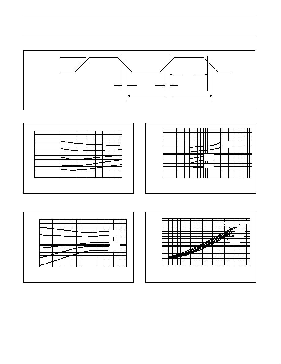
Philips Semiconductors
Preliminary data
P87LPC759
Low power, low price, low pin count (14 pin)
microcontroller with 1 kbyte OTP
2002 Mar 21
32
SU01188
V
DD
≠ 0.5
0.45V
0.2V
DD
+ 0.9
0.2 V
DD
≠ 0.1
t
CHCL
t
CLCH
t
CHCX
t
CLCX
t
C
Figure 29. External Clock Timing
SU01202
100
10
1
10
100
Idd (uA)
Frequency (kHz)
6.0 V
5.0 V
4.0 V
3.3 V
2.7 V
Figure 30. Typical Idd versus frequency (low frequency
oscillator, 25
∞
C)
SU01203
1000
100
10
100
10,000
Idd (uA)
Frequency (kHz)
1,000
6.0 V
5.0 V
2.7 V
6.0 V
5.0 V
4.0 V
3.3 V
2.7 V
Figure 31. Typical Idd versus frequency (medium frequency
oscillator, 25
∞
C)
SU01204
10,000
1,000
100
1
100
Idd (uA)
Frequency (MHz)
10
6.0 V
5.0 V
4.0 V
3.3 V
2.7 V
Figure 32. Typical Idd versus frequency (high frequency
oscillator, 25
∞
C)
SU01205
100,000
100
10
10
100,000
Idd (uA)
Frequency (kHz)
1,000
10,000
6.0 V
5.0 V
4.0 V
3.3 V
2.7 V
100
1,000
10,000
Figure 33. Typical Active Idd versus frequency (external clock,
25
∞
C, LPEP=0)

Philips Semiconductors
Preliminary data
P87LPC759
Low power, low price, low pin count (14 pin)
microcontroller with 1 kbyte OTP
2002 Mar 21
33
SU01206
10,000
100
1
10
10,000
Idd (uA)
Frequency (kHz)
4.0 V
3.3 V
2.7 V
100
1,000
1,000
10
Figure 34. Typical Active Idd versus frequency (external clock,
25
∞
C, LPEP=1)
SU01207
100
10
1
10
100
Idd (uA)
Frequency (kHz)
4.0 V
3.3 V
2.7 V
1,000
10,000
1,000
10,000
Figure 35. Typical Idle Idd versus frequency (external clock,
25
∞
C, LPEP=1)
SU01208
10,000
1,000
10
10
100,000
Idd (uA)
Frequency (kHz)
100
1,000
10,000
100
6.0 V
5.0 V
4.0 V
3.3 V
2.7 V
Figure 36. Typical Idle Idd versus frequency (external clock,
25
∞
C, LPEP=0)
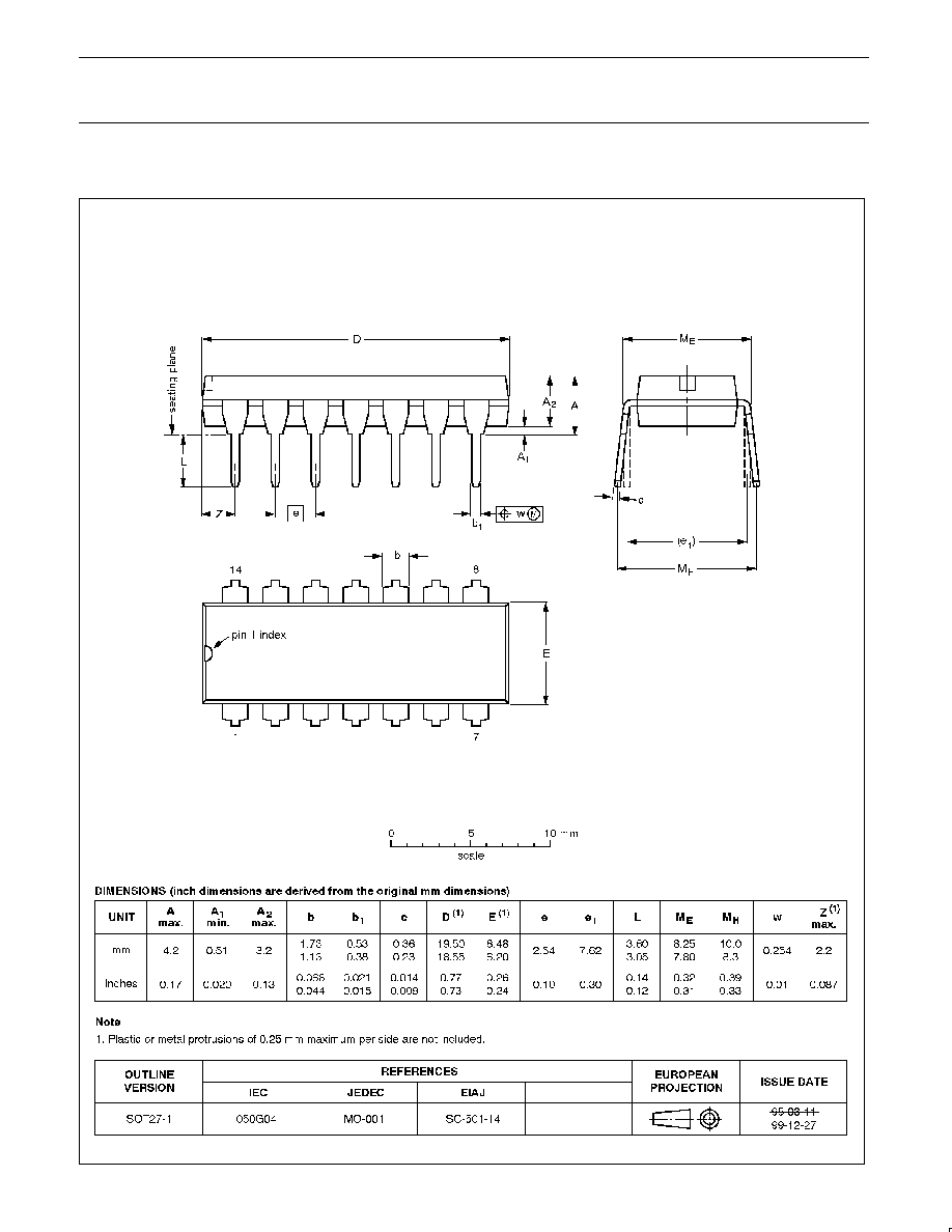
Philips Semiconductors
Preliminary data
P87LPC759
Low power, low price, low pin count (14 pin)
microcontroller with 1 kbyte OTP
2002 Mar 21
34
DIP14:
plastic dual in-line package; 14 leads (300 mil)
SOT27-1

Philips Semiconductors
Preliminary data
P87LPC759
Low power, low price, low pin count (14 pin)
microcontroller with 1 kbyte OTP
2002 Mar 21
35
REVISION HISTORY
Date
CPCN
Description
2002 Mar xx
9397 750
Initial release

Philips Semiconductors
Preliminary data
P87LPC759
Low power, low price, low pin count (14 pin)
microcontroller with 1 kbyte OTP
2002 Mar 21
36
Definitions
Short-form specification -- The data in a short-form specification is extracted from a full data sheet with the same type number and title. For
detailed information see the relevant data sheet or data handbook.
Limiting values definition -- Limiting values given are in accordance with the Absolute Maximum Rating System (IEC 60134). Stress above one
or more of the limiting values may cause permanent damage to the device. These are stress ratings only and operation of the device at these or
at any other conditions above those given in the Characteristics sections of the specification is not implied. Exposure to limiting values for extended
periods may affect device reliability.
Application information -- Applications that are described herein for any of these products are for illustrative purposes only. Philips
Semiconductors make no representation or warranty that such applications will be suitable for the specified use without further testing or
modification.
Disclaimers
Life support -- These products are not designed for use in life support appliances, devices or systems where malfunction of these products can
reasonably be expected to result in personal injury. Philips Semiconductors customers using or selling these products for use in such applications
do so at their own risk and agree to fully indemnify Philips Semiconductors for any damages resulting from such application.
Right to make changes -- Philips Semiconductors reserves the right to make changes, without notice, in the products, including circuits, standard
cells, and/or software, described or contained herein in order to improve design and/or performance. Philips Semiconductors assumes no
responsibility or liability for the use of any of these products, conveys no license or title under any patent, copyright, or mask work right to these
products, and makes no representations or warranties that these products are free from patent, copyright, or mask work right infringement, unless
otherwise specified.
Contact information
For additional information please visit
http://www.semiconductors.philips.com.
Fax: +31 40 27 24825
For sales offices addresses send e-mail to:
sales.addresses@www.semiconductors.philips.com.
©
Koninklijke Philips Electronics N.V. 2002
All rights reserved. Printed in U.S.A.
Date of release: 03-02
Document order number:
9397 750
Philips
Semiconductors
Data sheet status
[1]
Objective data
Preliminary data
Product data
Product
status
[2]
Development
Qualification
Production
Definitions
This data sheet contains data from the objective specification for product development.
Philips Semiconductors reserves the right to change the specification in any manner without notice.
This data sheet contains data from the preliminary specification. Supplementary data will be
published at a later date. Philips Semiconductors reserves the right to change the specification
without notice, in order to improve the design and supply the best possible product.
This data sheet contains data from the product specification. Philips Semiconductors reserves the
right to make changes at any time in order to improve the design, manufacturing and supply.
Changes will be communicated according to the Customer Product/Process Change Notification
(CPCN) procedure SNW-SQ-650A.
Data sheet status
[1] Please consult the most recently issued data sheet before initiating or completing a design.
[2] The product status of the device(s) described in this data sheet may have changed since this data sheet was published. The latest information is available on the Internet at URL
http://www.semiconductors.philips.com.