Document Outline
- GENERAL DESCRIPTION
- FEATURES
- ORDERING INFORMATION
- PIN CONFIGURATION
- LOGIC SYMBOL
- BLOCK DIAGRAM
- PIN DESCRIPTIONS
- SPECIAL FUNCTION REGISTERS
- FUNCTIONAL DESCRIPTION
- A/D Timing
- The A/D in Power Down and Idle Modes
- Code Examples for the A/D
- Analog Comparators
- I2C Serial Interface
- Interrupts
- I/O Ports
- Keyboard Interrupt (KBI)
- Oscillator
- Power Monitoring Functions
- Power Reduction Modes
- Reset
- Timer/Counters
- UART
- Watchdog Timer
- Additional Features
- EPROM Characteristics
- ABSOLUTE MAXIMUM RATINGS
- DC ELECTRICAL CHARACTERISTICS
- COMPARATOR ELECTRICAL CHARACTERISTICS
- A/D CONVERTER DC ELECTRICAL CHARACTERISTICS
- AC ELECTRICAL CHARACTERISTICS
- PACKAGE
- Data sheet status
- Definitions
- Disclaimers

Philips
Semiconductors
87LPC767
Low power, low price, low pin count
(20 pin) microcontroller with 4-kbyte OTP
and 8-bit A/D converter
Product data
Supersedes data of 2001 Jun 12
IC28 Data Handbook
2001 Aug 07
INTEGRATED CIRCUITS

Philips Semiconductors
Product data
87LPC767
Low power, low price, low pin count (20 pin)
microcontroller with 4-kbyte OTP and 8-bit A/D converter
2001 Aug 07
i
GENERAL DESCRIPTION
1
. . . . . . . . . . . . . . . . . . . . . . . . . . . . . . . . . . . . . . . . . . . . . . . . . . . . . . . . . . . . . . . . . . . . . . . . . . . . . . . .
FEATURES
1
. . . . . . . . . . . . . . . . . . . . . . . . . . . . . . . . . . . . . . . . . . . . . . . . . . . . . . . . . . . . . . . . . . . . . . . . . . . . . . . . . . . . . . . . . . . . .
ORDERING INFORMATION
2
. . . . . . . . . . . . . . . . . . . . . . . . . . . . . . . . . . . . . . . . . . . . . . . . . . . . . . . . . . . . . . . . . . . . . . . . . . . . . . .
PIN CONFIGURATION, 20-PIN DIP AND SO PACKAGES
2
. . . . . . . . . . . . . . . . . . . . . . . . . . . . . . . . . . . . . . . . . . . . . . . . . . . .
LOGIC SYMBOL
2
. . . . . . . . . . . . . . . . . . . . . . . . . . . . . . . . . . . . . . . . . . . . . . . . . . . . . . . . . . . . . . . . . . . . . . . . . . . . . . . . . . . . . . . . .
BLOCK DIAGRAM
3
. . . . . . . . . . . . . . . . . . . . . . . . . . . . . . . . . . . . . . . . . . . . . . . . . . . . . . . . . . . . . . . . . . . . . . . . . . . . . . . . . . . . . . .
PIN DESCRIPTIONS
5
. . . . . . . . . . . . . . . . . . . . . . . . . . . . . . . . . . . . . . . . . . . . . . . . . . . . . . . . . . . . . . . . . . . . . . . . . . . . . . . . . . . . .
SPECIAL FUNCTION REGISTERS
6
. . . . . . . . . . . . . . . . . . . . . . . . . . . . . . . . . . . . . . . . . . . . . . . . . . . . . . . . . . . . . . . . . . . . . . . . .
FUNCTIONAL DESCRIPTION
8
. . . . . . . . . . . . . . . . . . . . . . . . . . . . . . . . . . . . . . . . . . . . . . . . . . . . . . . . . . . . . . . . . . . . . . . . . . . . .
Enhanced CPU
8
. . . . . . . . . . . . . . . . . . . . . . . . . . . . . . . . . . . . . . . . . . . . . . . . . . . . . . . . . . . . . . . . . . . . . . . . . . . . . . . . . . . . . . . .
Analog Functions
8
. . . . . . . . . . . . . . . . . . . . . . . . . . . . . . . . . . . . . . . . . . . . . . . . . . . . . . . . . . . . . . . . . . . . . . . . . . . . . . . . . . . . . .
Analog to Digital Converter
8
. . . . . . . . . . . . . . . . . . . . . . . . . . . . . . . . . . . . . . . . . . . . . . . . . . . . . . . . . . . . . . . . . . . . . . . . . . . . . .
A/D Timing
9
. . . . . . . . . . . . . . . . . . . . . . . . . . . . . . . . . . . . . . . . . . . . . . . . . . . . . . . . . . . . . . . . . . . . . . . . . . . . . . . . . . . . . . . . . . . .
The A/D in Power Down and Idle Modes
10
. . . . . . . . . . . . . . . . . . . . . . . . . . . . . . . . . . . . . . . . . . . . . . . . . . . . . . . . . . . . . . . . . .
Code Examples for the A/D
11
. . . . . . . . . . . . . . . . . . . . . . . . . . . . . . . . . . . . . . . . . . . . . . . . . . . . . . . . . . . . . . . . . . . . . . . . . . . . .
Analog Comparators
12
. . . . . . . . . . . . . . . . . . . . . . . . . . . . . . . . . . . . . . . . . . . . . . . . . . . . . . . . . . . . . . . . . . . . . . . . . . . . . . . . . . .
Comparator Configuration
12
. . . . . . . . . . . . . . . . . . . . . . . . . . . . . . . . . . . . . . . . . . . . . . . . . . . . . . . . . . . . . . . . . . . . . . . . . . . .
Internal Reference Voltage
14
. . . . . . . . . . . . . . . . . . . . . . . . . . . . . . . . . . . . . . . . . . . . . . . . . . . . . . . . . . . . . . . . . . . . . . . . . . .
Comparator Interrupt
14
. . . . . . . . . . . . . . . . . . . . . . . . . . . . . . . . . . . . . . . . . . . . . . . . . . . . . . . . . . . . . . . . . . . . . . . . . . . . . . . .
Comparators and Power Reduction Modes
14
. . . . . . . . . . . . . . . . . . . . . . . . . . . . . . . . . . . . . . . . . . . . . . . . . . . . . . . . . . . . .
Comparator Configuration Example
14
. . . . . . . . . . . . . . . . . . . . . . . . . . . . . . . . . . . . . . . . . . . . . . . . . . . . . . . . . . . . . . . . . . . .
I2C Serial Interface
15
. . . . . . . . . . . . . . . . . . . . . . . . . . . . . . . . . . . . . . . . . . . . . . . . . . . . . . . . . . . . . . . . . . . . . . . . . . . . . . . . . . . .
I2C Interrupts
15
. . . . . . . . . . . . . . . . . . . . . . . . . . . . . . . . . . . . . . . . . . . . . . . . . . . . . . . . . . . . . . . . . . . . . . . . . . . . . . . . . . . . . . .
Reading I2CON
15
. . . . . . . . . . . . . . . . . . . . . . . . . . . . . . . . . . . . . . . . . . . . . . . . . . . . . . . . . . . . . . . . . . . . . . . . . . . . . . . . . . . . .
Checking ATN and DRDY
17
. . . . . . . . . . . . . . . . . . . . . . . . . . . . . . . . . . . . . . . . . . . . . . . . . . . . . . . . . . . . . . . . . . . . . . . . . . . .
Writing I2CON
17
. . . . . . . . . . . . . . . . . . . . . . . . . . . . . . . . . . . . . . . . . . . . . . . . . . . . . . . . . . . . . . . . . . . . . . . . . . . . . . . . . . . . . .
Regarding Transmit Active
17
. . . . . . . . . . . . . . . . . . . . . . . . . . . . . . . . . . . . . . . . . . . . . . . . . . . . . . . . . . . . . . . . . . . . . . . . . . .
Regarding Software Response Time
18
. . . . . . . . . . . . . . . . . . . . . . . . . . . . . . . . . . . . . . . . . . . . . . . . . . . . . . . . . . . . . . . . . . .
Interrupts
19
. . . . . . . . . . . . . . . . . . . . . . . . . . . . . . . . . . . . . . . . . . . . . . . . . . . . . . . . . . . . . . . . . . . . . . . . . . . . . . . . . . . . . . . . . . . . .
External Interrupt Inputs
20
. . . . . . . . . . . . . . . . . . . . . . . . . . . . . . . . . . . . . . . . . . . . . . . . . . . . . . . . . . . . . . . . . . . . . . . . . . . . . .
I/O Ports
21
. . . . . . . . . . . . . . . . . . . . . . . . . . . . . . . . . . . . . . . . . . . . . . . . . . . . . . . . . . . . . . . . . . . . . . . . . . . . . . . . . . . . . . . . . . . . . .
Quasi-Bidirectional Output Configuration
21
. . . . . . . . . . . . . . . . . . . . . . . . . . . . . . . . . . . . . . . . . . . . . . . . . . . . . . . . . . . . . . .
Open Drain Output Configuration
22
. . . . . . . . . . . . . . . . . . . . . . . . . . . . . . . . . . . . . . . . . . . . . . . . . . . . . . . . . . . . . . . . . . . . . .
Push-Pull Output Configuration
22
. . . . . . . . . . . . . . . . . . . . . . . . . . . . . . . . . . . . . . . . . . . . . . . . . . . . . . . . . . . . . . . . . . . . . . .
Keyboard Interrupt (KBI)
23
. . . . . . . . . . . . . . . . . . . . . . . . . . . . . . . . . . . . . . . . . . . . . . . . . . . . . . . . . . . . . . . . . . . . . . . . . . . . . . . .
Oscillator
25
. . . . . . . . . . . . . . . . . . . . . . . . . . . . . . . . . . . . . . . . . . . . . . . . . . . . . . . . . . . . . . . . . . . . . . . . . . . . . . . . . . . . . . . . . . . . .
Low Frequency Oscillator Option
25
. . . . . . . . . . . . . . . . . . . . . . . . . . . . . . . . . . . . . . . . . . . . . . . . . . . . . . . . . . . . . . . . . . . . . .
Medium Frequency Oscillator Option
25
. . . . . . . . . . . . . . . . . . . . . . . . . . . . . . . . . . . . . . . . . . . . . . . . . . . . . . . . . . . . . . . . . . .
High Frequency Oscillator Option
25
. . . . . . . . . . . . . . . . . . . . . . . . . . . . . . . . . . . . . . . . . . . . . . . . . . . . . . . . . . . . . . . . . . . . . .
On-Chip RC Oscillator Option
25
. . . . . . . . . . . . . . . . . . . . . . . . . . . . . . . . . . . . . . . . . . . . . . . . . . . . . . . . . . . . . . . . . . . . . . . . .
External Clock Input Option
25
. . . . . . . . . . . . . . . . . . . . . . . . . . . . . . . . . . . . . . . . . . . . . . . . . . . . . . . . . . . . . . . . . . . . . . . . . . .
Clock Output
25
. . . . . . . . . . . . . . . . . . . . . . . . . . . . . . . . . . . . . . . . . . . . . . . . . . . . . . . . . . . . . . . . . . . . . . . . . . . . . . . . . . . . . . .
CPU Clock Modification: CLKR and DIVM
27
. . . . . . . . . . . . . . . . . . . . . . . . . . . . . . . . . . . . . . . . . . . . . . . . . . . . . . . . . . . . . .
Power Monitoring Functions
27
. . . . . . . . . . . . . . . . . . . . . . . . . . . . . . . . . . . . . . . . . . . . . . . . . . . . . . . . . . . . . . . . . . . . . . . . . . . . .
Brownout Detection
27
. . . . . . . . . . . . . . . . . . . . . . . . . . . . . . . . . . . . . . . . . . . . . . . . . . . . . . . . . . . . . . . . . . . . . . . . . . . . . . . . .
Power On Detection
28
. . . . . . . . . . . . . . . . . . . . . . . . . . . . . . . . . . . . . . . . . . . . . . . . . . . . . . . . . . . . . . . . . . . . . . . . . . . . . . . . .
Power Reduction Modes
28
. . . . . . . . . . . . . . . . . . . . . . . . . . . . . . . . . . . . . . . . . . . . . . . . . . . . . . . . . . . . . . . . . . . . . . . . . . . . . . . .
Idle Mode
28
. . . . . . . . . . . . . . . . . . . . . . . . . . . . . . . . . . . . . . . . . . . . . . . . . . . . . . . . . . . . . . . . . . . . . . . . . . . . . . . . . . . . . . . . . .
Power Down Mode
28
. . . . . . . . . . . . . . . . . . . . . . . . . . . . . . . . . . . . . . . . . . . . . . . . . . . . . . . . . . . . . . . . . . . . . . . . . . . . . . . . . .
Low Voltage EPROM Operation
30
. . . . . . . . . . . . . . . . . . . . . . . . . . . . . . . . . . . . . . . . . . . . . . . . . . . . . . . . . . . . . . . . . . . . . . .
Reset
30
. . . . . . . . . . . . . . . . . . . . . . . . . . . . . . . . . . . . . . . . . . . . . . . . . . . . . . . . . . . . . . . . . . . . . . . . . . . . . . . . . . . . . . . . . . . . . . . .
Timer/Counters
31
. . . . . . . . . . . . . . . . . . . . . . . . . . . . . . . . . . . . . . . . . . . . . . . . . . . . . . . . . . . . . . . . . . . . . . . . . . . . . . . . . . . . . . . .
Mode 0
32
. . . . . . . . . . . . . . . . . . . . . . . . . . . . . . . . . . . . . . . . . . . . . . . . . . . . . . . . . . . . . . . . . . . . . . . . . . . . . . . . . . . . . . . . . . . .
Mode 1
33
. . . . . . . . . . . . . . . . . . . . . . . . . . . . . . . . . . . . . . . . . . . . . . . . . . . . . . . . . . . . . . . . . . . . . . . . . . . . . . . . . . . . . . . . . . . .

Philips Semiconductors
Product data
87LPC767
Low power, low price, low pin count (20 pin)
microcontroller with 4-kbyte OTP and 8-bit A/D converter
2001 Aug 07
ii
Mode 2
33
. . . . . . . . . . . . . . . . . . . . . . . . . . . . . . . . . . . . . . . . . . . . . . . . . . . . . . . . . . . . . . . . . . . . . . . . . . . . . . . . . . . . . . . . . . . .
Mode 3
33
. . . . . . . . . . . . . . . . . . . . . . . . . . . . . . . . . . . . . . . . . . . . . . . . . . . . . . . . . . . . . . . . . . . . . . . . . . . . . . . . . . . . . . . . . . . .
Timer Overflow Toggle Output
34
. . . . . . . . . . . . . . . . . . . . . . . . . . . . . . . . . . . . . . . . . . . . . . . . . . . . . . . . . . . . . . . . . . . . . . . .
UART
34
. . . . . . . . . . . . . . . . . . . . . . . . . . . . . . . . . . . . . . . . . . . . . . . . . . . . . . . . . . . . . . . . . . . . . . . . . . . . . . . . . . . . . . . . . . . . . . . .
Mode 0
34
. . . . . . . . . . . . . . . . . . . . . . . . . . . . . . . . . . . . . . . . . . . . . . . . . . . . . . . . . . . . . . . . . . . . . . . . . . . . . . . . . . . . . . . . . . . .
Mode 1
34
. . . . . . . . . . . . . . . . . . . . . . . . . . . . . . . . . . . . . . . . . . . . . . . . . . . . . . . . . . . . . . . . . . . . . . . . . . . . . . . . . . . . . . . . . . . .
Mode 2
34
. . . . . . . . . . . . . . . . . . . . . . . . . . . . . . . . . . . . . . . . . . . . . . . . . . . . . . . . . . . . . . . . . . . . . . . . . . . . . . . . . . . . . . . . . . . .
Mode 3
34
. . . . . . . . . . . . . . . . . . . . . . . . . . . . . . . . . . . . . . . . . . . . . . . . . . . . . . . . . . . . . . . . . . . . . . . . . . . . . . . . . . . . . . . . . . . .
Serial Port Control Register (SCON)
35
. . . . . . . . . . . . . . . . . . . . . . . . . . . . . . . . . . . . . . . . . . . . . . . . . . . . . . . . . . . . . . . . . . .
Baud Rates
36
. . . . . . . . . . . . . . . . . . . . . . . . . . . . . . . . . . . . . . . . . . . . . . . . . . . . . . . . . . . . . . . . . . . . . . . . . . . . . . . . . . . . . . . .
Using Timer 1 to Generate Baud Rates
36
. . . . . . . . . . . . . . . . . . . . . . . . . . . . . . . . . . . . . . . . . . . . . . . . . . . . . . . . . . . . . . . . .
More About UART Mode 0
38
. . . . . . . . . . . . . . . . . . . . . . . . . . . . . . . . . . . . . . . . . . . . . . . . . . . . . . . . . . . . . . . . . . . . . . . . . . .
More About UART Mode 1
38
. . . . . . . . . . . . . . . . . . . . . . . . . . . . . . . . . . . . . . . . . . . . . . . . . . . . . . . . . . . . . . . . . . . . . . . . . . .
More About UART Modes 2 and 3
41
. . . . . . . . . . . . . . . . . . . . . . . . . . . . . . . . . . . . . . . . . . . . . . . . . . . . . . . . . . . . . . . . . . . . .
Multiprocessor Communications
41
. . . . . . . . . . . . . . . . . . . . . . . . . . . . . . . . . . . . . . . . . . . . . . . . . . . . . . . . . . . . . . . . . . . . . . .
Automatic Address Recognition
44
. . . . . . . . . . . . . . . . . . . . . . . . . . . . . . . . . . . . . . . . . . . . . . . . . . . . . . . . . . . . . . . . . . . . . . .
Watchdog Timer
44
. . . . . . . . . . . . . . . . . . . . . . . . . . . . . . . . . . . . . . . . . . . . . . . . . . . . . . . . . . . . . . . . . . . . . . . . . . . . . . . . . . . . . . .
Watchdog Feed Sequence
44
. . . . . . . . . . . . . . . . . . . . . . . . . . . . . . . . . . . . . . . . . . . . . . . . . . . . . . . . . . . . . . . . . . . . . . . . . . .
Watchdog Reset
44
. . . . . . . . . . . . . . . . . . . . . . . . . . . . . . . . . . . . . . . . . . . . . . . . . . . . . . . . . . . . . . . . . . . . . . . . . . . . . . . . . . . .
Additional Features
46
. . . . . . . . . . . . . . . . . . . . . . . . . . . . . . . . . . . . . . . . . . . . . . . . . . . . . . . . . . . . . . . . . . . . . . . . . . . . . . . . . . . .
Software Reset
46
. . . . . . . . . . . . . . . . . . . . . . . . . . . . . . . . . . . . . . . . . . . . . . . . . . . . . . . . . . . . . . . . . . . . . . . . . . . . . . . . . . . . .
Dual Data Pointers
46
. . . . . . . . . . . . . . . . . . . . . . . . . . . . . . . . . . . . . . . . . . . . . . . . . . . . . . . . . . . . . . . . . . . . . . . . . . . . . . . . . .
EPROM Characteristics
47
. . . . . . . . . . . . . . . . . . . . . . . . . . . . . . . . . . . . . . . . . . . . . . . . . . . . . . . . . . . . . . . . . . . . . . . . . . . . . . . .
32-Byte Customer Code Space
47
. . . . . . . . . . . . . . . . . . . . . . . . . . . . . . . . . . . . . . . . . . . . . . . . . . . . . . . . . . . . . . . . . . . . . . .
System Configuration Bytes
47
. . . . . . . . . . . . . . . . . . . . . . . . . . . . . . . . . . . . . . . . . . . . . . . . . . . . . . . . . . . . . . . . . . . . . . . . . .
Security Bits
48
. . . . . . . . . . . . . . . . . . . . . . . . . . . . . . . . . . . . . . . . . . . . . . . . . . . . . . . . . . . . . . . . . . . . . . . . . . . . . . . . . . . . . . . .
ABSOLUTE MAXIMUM RATINGS
48
. . . . . . . . . . . . . . . . . . . . . . . . . . . . . . . . . . . . . . . . . . . . . . . . . . . . . . . . . . . . . . . . . . . . . . . . .
DC ELECTRICAL CHARACTERISTICS
49
. . . . . . . . . . . . . . . . . . . . . . . . . . . . . . . . . . . . . . . . . . . . . . . . . . . . . . . . . . . . . . . . . . . .
COMPARATOR ELECTRICAL CHARACTERISTICS
50
. . . . . . . . . . . . . . . . . . . . . . . . . . . . . . . . . . . . . . . . . . . . . . . . . . . . . . . . .
A/D CONVERTER DC ELECTRICAL CHARACTERISTICS
50
. . . . . . . . . . . . . . . . . . . . . . . . . . . . . . . . . . . . . . . . . . . . . . . . . . .
AC ELECTRICAL CHARACTERISTICS
52
. . . . . . . . . . . . . . . . . . . . . . . . . . . . . . . . . . . . . . . . . . . . . . . . . . . . . . . . . . . . . . . . . . . .

Philips Semiconductors
Product data
87LPC767
Low power, low price, low pin count (20 pin)
microcontroller with 4-kbyte OTP and 8-bit A/D converter
1
2001 Aug 07
853-2255 26851
GENERAL DESCRIPTION
The 87LPC767 is a 20-pin single-chip microcontroller designed for
low pin count applications demanding high-integration, low cost
solutions over a wide range of performance requirements. A
member of the Philips low pin count family, the 87LPC767 offers
programmable oscillator configurations for high and low speed
crystals or RC operation, wide operating voltage range,
programmable port output configurations, selectable Schmitt trigger
inputs, LED drive outputs, and a built-in watchdog timer. The
87LPC767 is based on an accelerated 80C51 processor
architecture that executes instructions at twice the rate of standard
80C51 devices.
FEATURES
∑
An accelerated 80C51 CPU provides instruction cycle times of
300≠600 ns for all instructions except multiply and divide when
executing at 20 MHz. Execution at up to 20 MHz when
V
DD
= 4.5 V to 6.0 V, 10 MHz when V
DD
= 2.7 V to 6.0 V.
∑
Four-channel multiplexed 8-bit A/D converter. Conversion time of
9.3
µ
S at f
OSC
= 20 MHz.
∑
2.7 V to 6.0 V operating range for digital functions.
∑
4 K bytes EPROM code memory.
∑
128 byte RAM data memory.
∑
32-byte customer code EPROM allows serialization of devices,
storage of setup parameters, etc.
∑
Two 16-bit counter/timers. Each timer may be configured to toggle
a port output upon timer overflow.
∑
Two analog comparators.
∑
Full duplex UART.
∑
I
2
C communication port.
∑
Eight keypad interrupt inputs, plus two additional external interrupt
inputs.
∑
Four interrupt priority levels.
∑
Watchdog timer with separate on-chip oscillator, requiring no
external components. The watchdog timeout time is selectable
from 8 values.
∑
Active low reset. On-chip power-on reset allows operation with no
external reset components.
∑
Low voltage reset. One of two preset low voltage levels may be
selected to allow a graceful system shutdown when power fails.
May optionally be configured as an interrupt.
∑
Oscillator Fail Detect. The watchdog timer has a separate fully
on-chip oscillator, allowing it to perform an oscillator fail detect
function.
∑
Configurable on-chip oscillator with frequency range and RC
oscillator options (selected by user programmed EPROM bits).
The RC oscillator option allows operation with no external
oscillator components.
∑
Programmable port output configuration options:
quasi-bidirectional, open drain, push-pull, input-only.
∑
Selectable Schmitt trigger port inputs.
∑
LED drive capability (20 mA) on all port pins.
∑
Controlled slew rate port outputs to reduce EMI. Outputs have
approximately 10 ns minimum ramp times.
∑
15 I/O pins minimum. Up to 18 I/O pins using on-chip oscillator
and reset options.
∑
Only power and ground connections are required to operate the
87LPC767 when fully on-chip oscillator and reset options are
selected.
∑
Serial EPROM programming allows simple in-circuit production
coding. Two EPROM security bits prevent reading of sensitive
application programs.
∑
Idle and Power Down reduced power modes. Improved wakeup
from Power Down mode (a low interrupt input starts execution).
Typical Power Down current is 1
µ
A.
∑
20-pin DIP and SO packages.
Philips Semiconductors
Product data
87LPC767
Low power, low price, low pin count (20 pin)
microcontroller with 4-kbyte OTP and 8-bit A/D converter
2001 Aug 07
2
ORDERING INFORMATION
Type number
Package
Temperature
R
(
∞
C)
Name
Description
Version
Range (
∞
C)
P87LPC767BN
DIP20
plastic dual in-line package; 20 leads (300 mil)
SOT146-1
0 to +70
P87LPC767BD
SO20
plastic small outline package; 20 leads; body width 7.5 mm
SOT163-1
0 to +70
P87LPC767FN
DIP20
plastic dual in-line package; 20 leads (300 mil)
SOT146-1
≠40 to +85
P87LPC767FD
SO20
plastic small outline package; 20 leads; body width 7.5 mm
SOT163-1
≠40 to +85
P87LPC767HD
SO20
plastic small outline package; 20 leads; body width 7.5 mm
SOT163-1
≠40 to +125
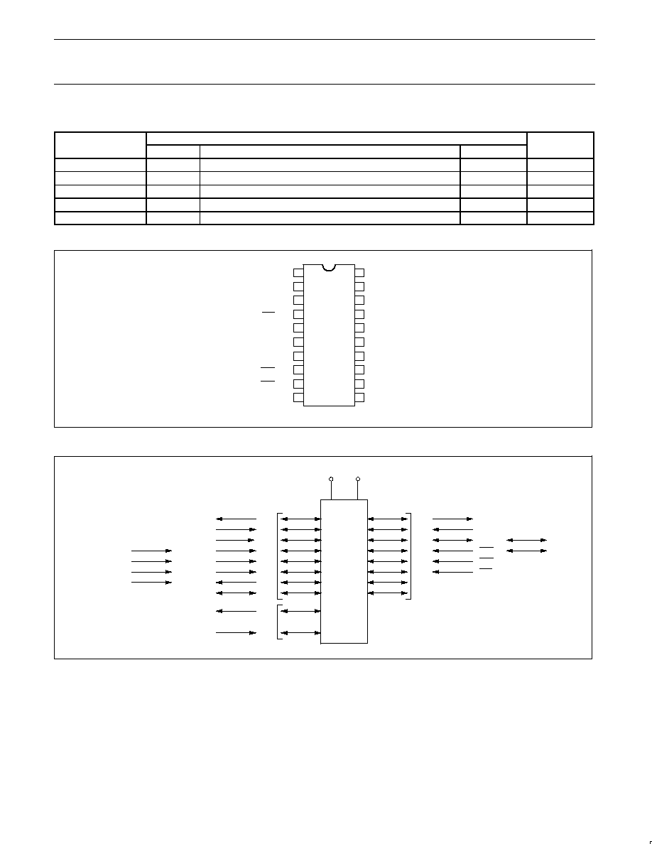
PIN CONFIGURATION, 20-PIN DIP AND SO PACKAGES
SU01349
1
2
3
4
5
6
7
8
9
11
12
13
14
15
16
17
18
19
20
CMP2/P0.0
P1.7
P1.6
RST/P1.5
V
SS
X1/P2.1
X2/CLKOUT/P2.0
INT1/P1.4
SDA/INT0/P1.3
SCL/T0/P1.2
P0.1/CIN2B
P0.2/CIN2A
P0.3/CIN1B/AD0
P0.4/CIN1A/AD1
P0.5/CMPREF/AD2
V
DD
P0.6/CMP1/AD3
P1.0/TxD
P0.7/T1
P1.1/RxD
10
LOGIC SYMBOL
T1
X1
SU01350
V
DD
V
SS
TxD
CMP2
CIN2B
CIN2A
CIN1B
CIN1A
CMPREF
CMP1
CLKOUT/X2
PORT 0
PORT 2
PORT 1
RxD
INT0
RST
INT1
T0
SCL
SDA
AD0
AD1
AD2
AD3
Philips Semiconductors
Product data
87LPC767
Low power, low price, low pin count (20 pin)
microcontroller with 4-kbyte OTP and 8-bit A/D converter
2001 Aug 07
3
BLOCK DIAGRAM
SU01351
TIMER 0, 1
I
2
C
UART
ACCELERATED
80C51 CPU
WATCHDOG TIMER
AND OSCILLATOR
PORT 0
CONFIGURABLE I/OS
128 BYTE
DATA RAM
4K BYTE
CODE EPROM
INTERNAL BUS
ANALOG
COMPARATORS
PORT 1
CONFIGURABLE I/OS
KEYPAD
INTERRUPT
PORT 2
CONFIGURABLE I/OS
POWER MONITOR
(POWER-ON RESET,
BROWNOUT RESET)
CONFIGURABLE
OSCILLATOR
CRYSTAL OR
RESONATOR
ON-CHIP
R/C
OSCILLATOR
A/D
CONVERTER
Philips Semiconductors
Product data
87LPC767
Low power, low price, low pin count (20 pin)
microcontroller with 4-kbyte OTP and 8-bit A/D converter
2001 Aug 07
4
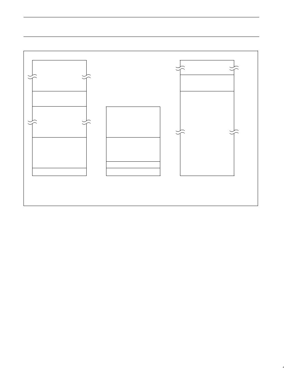
SU01352
UNUSED CODE
MEMORY SPACE
32-BYTE CUSTOMER
CODE SPACE
(ACCESSIBLE VIA MOVC)
UNUSED CODE
MEMORY SPACE
4 K BYTES ON-CHIP
CODE MEMORY
INTERRUPT VECTORS
SPECIAL FUNCTION
REGISTERS
(ONLY DIRECTLY
ADDRESSABLE)
128 BYTES ON-CHIP DATA
MEMORY
(DIRECTLY AND
INDIRECTLY
ADDRESSABLE)
16-BIT ADDRESSABLE BYTES
UNUSED SPACE
CONFIGURATION BYTES
UCFG1, UCFG2
(ACCESSIBLE VIA MOVX)
UNUSED SPACE
FFFFh
FCFFh
FCE0h
1000h
0FFFh
FFh
80h
7Fh
0000h
00h
0000h
FD00h
FD01h
FFFFh
*
The 87LPC767 does not support access to external data memory. However, the User Configuration Bytes
are accessed via the MOVX instruction as if they were in external data memory.
ON-CHIP CODE
MEMORY SPACE
ON-CHIP DATA
MEMORY SPACE
EXTERNAL DATA
MEMORY SPACE*
Figure 1. 87LPC767 Program and Data Memory Map

Philips Semiconductors
Product data
87LPC767
Low power, low price, low pin count (20 pin)
microcontroller with 4-kbyte OTP and 8-bit A/D converter
2001 Aug 07
5
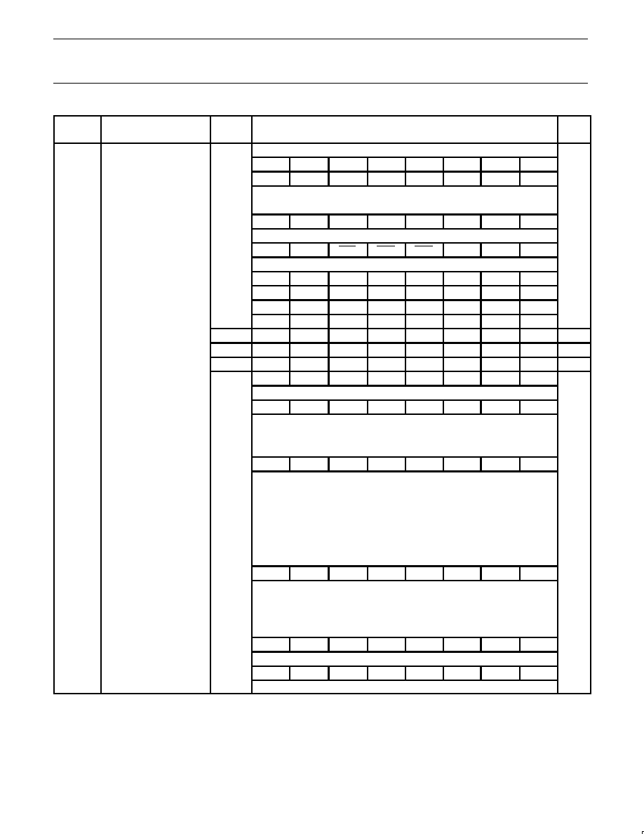
PIN DESCRIPTIONS
MNEMONIC
PIN NO.
TYPE
NAME AND FUNCTION
P0.0≠P0.7
1, 13, 14,
16≠20
I/O
Port 0: Port 0 is an 8-bit I/O port with a user-configurable output type. Port 0 latches are configured in
the quasi-bidirectional mode and have either ones or zeros written to them during reset, as determined
by the PRHI bit in the UCFG1 configuration byte. The operation of port 0 pins as inputs and outputs
depends upon the port configuration selected. Each port pin is configured independently. Refer to the
section on I/O port configuration and the DC Electrical Characteristics for details.
The Keyboard Interrupt feature operates with port 0 pins.
Port 0 also provides various special functions as described below.
1
O
P0.0
CMP2
Comparator 2 output.
20
I
P0.1
CIN2B
Comparator 2 positive input B.
19
I
P0.2
CIN2A
Comparator 2 positive input A.
18
I
P0.3
CIN1B
Comparator 1 positive input B.
I
AD0
A/D channel 0 input.
17
I
P0.4
CIN1A
Comparator 1 positive input A.
I
AD1
A/D channel 1 input.
16
I
P0.5
CMPREF
Comparator reference (negative) input.
I
AD2
A/D channel 2 input.
14
O
P0.6
CMP1
Comparator 1 output.
I
AD3
A/D channel 3 input.
13
I/O
P0.7
T1
Timer/counter 1 external count input or overflow output.
P1.0≠P1.7
2≠4, 8≠12
I/O
Port 1: Port 1 is an 8-bit I/O port with a user-configurable output type, except for three pins as noted
below. Port 1 latches are configured in the quasi-bidirectional mode and have either ones or zeros
written to them during reset, as determined by the PRHI bit in the UCFG1 configuration byte. The
operation of the configurable port 1 pins as inputs and outputs depends upon the port configuration
selected. Each of the configurable port pins are programmed independently. Refer to the section on I/O
port configuration and the DC Electrical Characteristics for details.
Port 1 also provides various special functions as described below.
12
O
P1.0
TxD
Transmitter output for the serial port.
11
I
P1.1
RxD
Receiver input for the serial port.
10
I/O
I/O
P1.2
T0
Timer/counter 0 external count input or overflow output.
SCL
I
2
C serial clock input/output. When configured as an output, P1.2 is open
drain, in order to conform to I
2
C specifications.
9
I
I/O
P1.3
INT0
External interrupt 0 input.
SDA
I
2
C serial data input/output. When configured as an output, P1.3 is open
drain, in order to conform to I
2
C specifications.
8
I
P1.4
INT1
External interrupt 1 input.
4
I
P1.5
RST
External Reset input (if selected via EPROM configuration). A low on this pin
resets the microcontroller, causing I/O ports and peripherals to take on their
default states, and the processor begins execution at address 0. When used
as a port pin, P1.5 is a Schmitt trigger input only.

Philips Semiconductors
Product data
87LPC767
Low power, low price, low pin count (20 pin)
microcontroller with 4-kbyte OTP and 8-bit A/D converter
2001 Aug 07
6
P2.0≠P2.1
6, 7
I/O
Port 2: Port 2 is a 2-bit I/O port with a user-configurable output type. Port 2 latches are configured in the
quasi-bidirectional mode and have either ones or zeros written to them during reset, as determined by
the PRHI bit in the UCFG1 configuration byte. The operation of port 2 pins as inputs and outputs
depends upon the port configuration selected. Each port pin is configured independently. Refer to the
section on I/O port configuration and the DC Electrical Characteristics for details.
Port 2 also provides various special functions as described below.
7
O
P2.0
X2
Output from the oscillator amplifier (when a crystal oscillator option is
selected via the EPROM configuration).
CLKOUT
CPU clock divided by 6 clock output when enabled via SFR bit and in
conjunction with internal RC oscillator or external clock input.
6
I
P2.1
X1
Input to the oscillator circuit and internal clock generator circuits (when
selected via the EPROM configuration).
V
SS
5
I
Ground: 0 V reference.
V
DD
15
I
Power Supply: This is the power supply voltage for normal operation as well as Idle and
Power Down modes.
SPECIAL FUNCTION REGISTERS
Name
Description
SFR
Address
Bit Functions and Addresses
MSB
LSB
Reset
Value
E7
E6
E5
E4
E3
E2
E1
E0
ACC*
Accumulator
E0h
00h
C7
C6
C5
C4
C3
C2
C1
C0
ADCON#*
A/D Control
C0h
ENADC
≠
≠
ADCI
ADCS
RCCLK
AADR1
AADR0
00h
AUXR1#
Auxiliary Function Register
A2h
KBF
BOD
BOI
LPEP
SRST
0
≠
DPS
02h
1
F7
F6
F5
F4
F3
F2
F1
F0
B*
B register
F0h
00h
CMP1#
Comparator 1 control
register
ACh
≠
≠
CE1
CP1
CN1
OE1
CO1
CMF1
00h
1
CMP2#
Comparator 2 control
register
ADh
≠
≠
CE2
CP2
CN2
OE2
CO2
CMF2
00h
1
DAC0#
A/D Result
C5h
00h
DIVM#
CPU clock divide-by-M
control
95h
00h
DPTR:
Data pointer (2 bytes)
DPH
Data pointer high byte
83h
00h
DPL
Data pointer low byte
82h
00h
CF
CE
CD
CC
CB
CA
C9
C8
I2CFG#*
I
2
C configuration register
C8h/RD
SLAVEN
MASTRQ
0
TIRUN
≠
≠
CT1
CT0
00h
1
C8h/WR
SLAVEN
MASTRQ
CLRTI
TIRUN
≠
≠
CT1
CT0
DF
DE
DD
DC
DB
DA
D9
D8
I2CON#*
I
2
C control register
D8h/RD
RDAT
ATN
DRDY
ARL
STR
STP
MASTER
≠
80h
1
D8h/WR
CXA
IDLE
CDR
CARL
CSTR
CSTP
XSTR
XSTP
I2DAT#
I
2
C data register
D9h/RD
RDAT
0
0
0
0
0
0
0
80h
D9h/WR
XDAT
x
x
x
x
x
x
x
AF
AE
AD
AC
AB
AA
A9
A8
IEN0*
Interrupt enable 0
A8h
EA
EWD
EBO
ES
ET1
EX1
ET0
EX0
00h
EF
EE
ED
EC
EB
EA
E9
E8
IEN1#*
Interrupt enable 1
E8h
ETI
≠
EC1
EAD
≠
EC2
EKB
EI2
00h
1
BF
BE
BD
BC
BB
BA
B9
B8
IP0*
Interrupt priority 0
B8h
≠
PWD
PBO
PS
PT1
PX1
PT0
PX0
00h
1
IP0H#
Interrupt priority 0 high byte
B7h
≠
PWDH
PBOH
PSH
PT1H
PX1H
PT0H
PX0H
00h
1
Philips Semiconductors
Product data
87LPC767
Low power, low price, low pin count (20 pin)
microcontroller with 4-kbyte OTP and 8-bit A/D converter
2001 Aug 07
7
Name
Reset
Value
Bit Functions and Addresses
MSB
LSB
SFR
Address
Description
FF
FE
FD
FC
FB
FA
F9
F8
IP1*
Interrupt priority 1
F8h
PTI
≠
PC1
PAD
≠
PC2
PKB
PI2
00h
1
IP1H#
Interrupt priority 1 high byte
F7h
PTIH
≠
PC1H
PADH
≠
PC2H
PKBH
PI2H
00h
1
KBI#
Keyboard Interrupt
86h
00h
87
86
85
84
83
82
81
80
P0*
Port 0
80h
T1
CMP1
CMPREF
CIN1A
CIN1B
CIN2A
CIN2B
CMP2
Note 2
97
96
95
94
93
92
91
90
P1*
Port 1
90h
(P1.7)
(P1.6)
RST
INT1
INT0
T0
RxD
TxD
Note 2
A7
A6
A5
A4
A3
A2
A1
A0
P2*
Port 2
A0h
≠
≠
≠
≠
≠
≠
X1
X2
Note 2
P0M1#
Port 0 output mode 1
84h
(P0M1.7)
(P0M1.6)
(P0M1.5)
(P0M1.4)
(P0M1.3)
(P0M1.2)
(P0M1.1)
(P0M1.0)
00h
P0M2#
Port 0 output mode 2
85h
(P0M2.7)
(P0M2.6)
(P0M2.5)
(P0M2.4)
(P0M2.3)
(P0M2.2)
(P0M2.1)
(P0M2.0)
00H
P1M1#
Port 1 output mode 1
91h
(P1M1.7)
(P1M1.6)
≠
(P1M1.4)
≠
≠
(P1M1.1)
(P1M1.0)
00h
1
P1M2#
Port 1 output mode 2
92h
(P1M2.7)
(P1M2.6)
≠
(P1M2.4)
≠
≠
(P1M2.1)
(P1M2.0)
00h
1
P2M1#
Port 2 output mode 1
A4h
P2S
P1S
P0S
ENCLK
T1OE
T0OE
(P2M1.1)
(P2M1.0)
00h
P2M2#
Port 2 output mode 2
A5h
≠
≠
≠
≠
≠
≠
(P2M2.1)
(P2M2.0)
00h
1
PCON
Power control register
87h
SMOD1
SMOD0
BOF
POF
GF1
GF0
PD
IDL
Note 3
D7
D6
D5
D4
D3
D2
D1
D0
PSW*
Program status word
D0h
CY
AC
F0
RS1
RS0
OV
F1
P
00h
PT0AD#
Port 0 digital input disable
F6h
00h
9F
9E
9D
9C
9B
9A
99
98
SCON*
Serial port control
98h
SM0
SM1
SM2
REN
TB8
RB8
TI
RI
00h
SBUF
Serial port data buffer
register
99h
xxh
SADDR#
Serial port address register
A9h
00h
SADEN#
Serial port address enable
B9h
00h
SP
Stack pointer
81h
07h
8F
8E
8D
8C
8B
8A
89
88
TCON*
Timer 0 and 1 control
88h
TF1
TR1
TF0
TR0
IE1
IT1
IE0
IT0
00h
TH0
Timer 0 high byte
8Ch
00h
TH1
Timer 1 high byte
8Dh
00h
TL0
Timer 0 low byte
8Ah
00h
TL1
Timer 1 low byte
8Bh
00h
TMOD
Timer 0 and 1 mode
89h
GATE
C/T
M1
M0
GATE
C/T
M1
M0
00h
WDCON#
Watchdog control register
A7h
≠
≠
WDOVF
WDRUN
WDCLK
WDS2
WDS1
WDS0
Note 4
WDRST#
Watchdog reset register
A6h
xxh
NOTES:
* SFRs are bit addressable.
# SFRs are modified from or added to the 80C51 SFRs.
1. Unimplemented bits in SFRs are X (unknown) at all times. Ones should not be written to these bits since they may be used for other
purposes in future derivatives. The reset value shown in the table for these bits is 0.
2. I/O port values at reset are determined by the PRHI bit in the UCFG1 configuration byte.
3. The PCON reset value is x x BOF POF≠0 0 0 0b. The BOF and POF flags are not affected by reset. The POF flag is set by hardware upon
power up. The BOF flag is set by the occurrence of a brownout reset/interrupt and upon power up.
4. The WDCON reset value is xx11 0000b for a Watchdog reset, xx01 0000b for all other reset causes if the watchdog is enabled, and xx00
0000b for all other reset causes if the watchdog is disabled.

Philips Semiconductors
Product data
87LPC767
Low power, low price, low pin count (20 pin)
microcontroller with 4-kbyte OTP and 8-bit A/D converter
2001 Aug 07
8
FUNCTIONAL DESCRIPTION
Details of 87LPC767 functions will be described in the following
sections.
Enhanced CPU
The 87LPC767 uses an enhanced 80C51 CPU which runs at twice the
speed of standard 80C51 devices. This means that the performance of
the 87LPC767 running at 5 MHz is exactly the same as that of a
standard 80C51 running at 10 MHz. A machine cycle consists of 6
oscillator cycles, and most instructions execute in 6 or 12 clocks. A
user configurable option allows restoring standard 80C51 execution
timing. In that case, a machine cycle becomes 12 oscillator cycles.
In the following sections, the term "CPU clock" is used to refer to the
clock that controls internal instruction execution. This may
sometimes be different from the externally applied clock, as in the
case where the part is configured for standard 80C51 timing by
means of the CLKR configuration bit or in the case where the clock
is divided down via the setting of the DIVM register. These features
are described in the Oscillator section.
Analog Functions
The 87LPC767 incorporates analog peripheral functions: an Analog
to Digital Converter and two Analog Comparators. In order to give
the best analog function performance and to minimize power
consumption, pins that are being used for analog functions must
have the digital outputs and inputs disabled.
Digital outputs are disabled by putting the port output into the Input
Only (high impedance) mode as described in the I/O Ports section.
Digital inputs on port 0 may be disabled through the use of the
PT0AD register. Each bit in this register corresponds to one pin of
Port 0. Setting the corresponding bit in PT0AD disables that pin's
digital input. Port bits that have their digital inputs disabled will be
read as 0 by any instruction that accesses the port.
Analog to Digital Converter
The 87LPC767 incorporates a four channel, 8-bit A/D converter. The
A/D inputs are alternate functions on four port 0 pins. Because the
device has a very limited number of pins, the A/D power supply and
references are shared with the processor power pins, V
DD
and V
SS
.
The A/D converter operates down to a V
DD
supply of 3.0 V.
The A/D converter circuitry consists of a 4-input analog multiplexer
and an 8-bit successive approximation ADC. The A/D employs a
ratiometric potentiometer which guarantees DAC monotonicity.
The A/D converter is controlled by the special function register
ADCON. Details of ADCON are shown in Figure 2. The A/D must be
enabled by setting the ENADC bit at least 10 microseconds before a
conversion is started, to allow time for the A/D to stabilize. Prior to
the beginning of an A/D conversion, one analog input pin must be
selected for conversion via the AADR1 and AADR0 bits. These bits
cannot be changed while the A/D is performing a conversion.
An A/D conversion is started by setting the ADCS bit, which remains
set while the conversion is in progress. When the conversion is
complete, the ADCS bit is cleared and the ADCI bit is set. When
ADCI is set, it will generate an interrupt if the interrupt system is
enabled, the A/D interrupt is enabled (via the EAD bit in the IE1
register), and the A/D interrupt is the highest priority pending
interrupt.
When a conversion is complete, the result is contained in the
register DAC0. This value will not change until another conversion is
started. Before another A/D conversion may be started, the ADCI bit
must be cleared by software. The A/D channel selection may be
changed by the same instruction that sets ADCS to start a new
conversion, but not by the same instruction that clears ADCI.
The connections of the A/D converter are shown in Figure 3.
The ideal A/D result may be calculated as follows:
Result
+
(V
IN
≠V
SS
) x
256
V
DD
≠V
SS
(round result to the nearest integer)

Philips Semiconductors
Product data
87LPC767
Low power, low price, low pin count (20 pin)
microcontroller with 4-kbyte OTP and 8-bit A/D converter
2001 Aug 07
9
ADCON
Address: C0h
Bit addressable
Reset Value: 00h
BIT
SYMBOL
FUNCTION
ADCON.7
ENADC
When ENADC = 1, the A/D is enabled and conversions may take place. Must be set 10
microseconds before a conversion is started. ENADC cannot be cleared while ADCS or ADCI
are 1.
ADCON.6
-
Reserved for future use. Should not be set to 1 by user programs.
ADCON.5
-
Reserved for future use. Should not be set to 1 by user programs.
ADCON.4
ADCI
A/D conversion complete/interrupt flag. This flag is set when an A/D conversion is completed.
This bit will cause a hardware interrupt if enabled and of sufficient priority. Must be cleared by
software.
ADCON.3
ADCS
A/D start. Setting this bit by software starts the conversion of the selected A/D input. ADCS
remains set while the A/D conversion is in progress and is cleared automatically upon
completion. While ADCS or ADCI are one, new start commands are ignored.
ADCI, ADCS
A/D Status
0 0
A/D not busy, a conversion can be started.
0 1
A/D busy, the start of a new conversion is blocked.
1 0
An A/D conversion is complete. ADCI must be cleared prior to starting a new conversion.
1 1
An A/D conversion is complete. ADCI must be cleared prior to starting a new conversion. This
state exists for one machine cycle as an A/D conversion is completed.
ADCON.2
RCCLK
When RCCLK = 0, the CPU clock is used as the A/D clock. When RCCLK = 1, the internal RC
oscillator is used as the A/D clock. This bit is writable while ADCS and ADCI are 0.
ADCON.1, 0
AADR1,0
Along with AADR0, selects the A/D channel to be converted. These bits can only be written
while ADCS and ADCI are 0.
AADR1, AADR0
A/D Input Selected
0 0
AD0 (P0.3).
0 1
AD1 (P0.4).
1 0
AD2 (P0.5).
1 1
AD3 (P0.6).
7
6
5
4
3
2
1
0
ENADC
-
-
ADCI
ADCS
RCCLK
AADR1
AADR0
SU01354
Figure 2. A/D Control Register (ADCON)
A/D Timing
The A/D may be clocked in one of two ways. The default is to use
the CPU clock as the A/D clock source. When used in this manner,
the A/D completes a conversion in 31 machine cycles. The A/D may
be operated up to the maximum CPU clock rate of 20 MHz, giving a
conversion time of 9.3
µ
s. The formula for calculating A/D
conversion time when the CPU clock runs the A/D is: 186
µ
s / CPU
clock rate (in MHz). To obtain accurate A/D conversion results, the
CPU clock must be at least 1 MHz.
The A/D may also be clocked by the on-chip RC oscillator, even if
the RC oscillator is not used as the CPU clock. This is accomplished
by setting the RCCLK bit in ADCON. This arrangement has several
advantages. First, the A/D conversion time is faster at lower CPU
clock rates. Also, the CPU may be run at speeds below 1 MHz
without affecting A/D accuracy. Finally, the Power Down mode may
be used to completely shut down the CPU and its oscillator, along
with other peripheral functions, in order to obtain the best possible
A/D accuracy. This should not be used if the MCU uses an external
clock source greater than 4 MHz.
When the A/D is operated from the RCCLK while the CPU is running
from another clock source, 3 or 4 machine cycles are used to
synchronize A/D operation. The time can range from a minimum of 3
machine cycles (at the CPU clock rate) + 108 RC clocks to a
maximum of 4 machine cycles (at the CPU clock rate) + 112 RC
clocks.
Example A/D conversion times at various CPU clock rates are
shown in Table 1. In Table 1, maximum times for RCCLK = 1 use an
RC clock frequency of 4.5 MHz (6 MHz - 25%). Minimum times for
RCCLK = 1 use an RC clock frequency of 7.5 MHz (6 MHz + 25%).
Nominal time assume an ideal RC clock frequency of 6 MHz and an
average of 3.5 machine cycles at the CPU clock rate.

Philips Semiconductors
Product data
87LPC767
Low power, low price, low pin count (20 pin)
microcontroller with 4-kbyte OTP and 8-bit A/D converter
2001 Aug 07
10
Table 1. Example A/D Conversion Times
CPU Clock Rate
RCCLK = 0
RCCLK = 1
CPU Clock Rate
RCCLK = 0
minimum
nominal
maximum
32 kHz
NA
563.4
µ
s
659
µ
s
757
µ
s
1 MHz
186
µ
s
32.4
µ
s
39.3
µ
s
48.9
µ
s
4 MHz
46.5
µ
s
18.9
µ
s
23.6
µ
s
30.1
µ
s
11.0592 MHz
16.8
µ
s
16
µ
s
20.2
µ
s
27.1
µ
s
12 MHz
15.5
µ
s
16 MHz
11.6
µ
s
20 MHz
9.3
µ
s
Note: Do not clock ADC from the RC oscillator when MCU clock is greater than 4 MHz.
AD0 (P0.3)
AD1 (P0.4)
V
REF
+ = V
DD
AADR1
AD2 (P0.5)
AD3 (P0.6)
00
01
10
11
V
REF
- = V
SS
ADCON
A/D Converter
AADR0
DAC0
(A/D result)
SU01356
Figure 3. A/D Converter Connections
The A/D in Power Down and Idle Modes
While using the CPU clock as the A/D clock source, the Idle mode
may be used to conserve power and/or to minimize system noise
during the conversion. CPU operation will resume and Idle mode
terminate automatically when a conversion is complete if the A/D
interrupt is active. In Idle mode, noise from the CPU itself is
eliminated, but noise from the oscillator and any other on-chip
peripherals that are running will remain.
The CPU may be put into Power Down mode when the A/D is
clocked by the on-chip RC oscillator (RCCLK = 1). This mode gives
the best possible A/D accuracy by eliminating most on-chip noise
sources.
If the Power Down mode is entered while the A/D is running from the
CPU clock (RCCLK = 0), the A/D will abort operation and will not
wake up the CPU. The contents of DAC0 will be invalid when
operation does resume.
When an A/D conversion is started, Power Down or Idle mode must
be activated within two machine cycles in order to have the most
accurate A/D result. These two machine cycles are counted at the
CPU clock rate. When using the A/D with either Power Down or Idle
mode, care must be taken to insure that the CPU is not restarted by
another interrupt until the A/D conversion is complete. The possible
causes of wakeup are different in Power Down and Idle modes.
A/D accuracy is also affected by noise generated elsewhere in the
application, power supply noise, and power supply regulation. Since
the 87LPC767 power pins are also used as the A/D reference and
supply, the power supply has a very direct affect on the accuracy of
A/D readings. Using the A/D without Power Down mode while the
clock is divided through the use of CLKR or DIVM has an adverse
effect on A/D accuracy.

Philips Semiconductors
Product data
87LPC767
Low power, low price, low pin count (20 pin)
microcontroller with 4-kbyte OTP and 8-bit A/D converter
2001 Aug 07
11
Code Examples for the A/D
The first piece of sample code shows an example of port configuration for use with the A/D. This example sets up the pins so that all four A/D
channels may be used. Port configuration for analog functions is described in the section Analog Functions.
; Set up port pins for A/D conversion, without affecting other pins.
mov
PT0AD,#78h
; Disable digital inputs on A/D input pins.
anl
P0M2,#87h
; Disable digital outputs on A/D input pins.
orl
P0M1,#78h
; Disable digital outputs on A/D input pins.
Following is an example of using the A/D with interrupts. The routine ADStart begins an A/D conversion using the A/D channel number supplied
in the accumulator. The channel number is not checked for validity. The A/D must previously have been enabled with sufficient time to allow for
stabilization.
The interrupt handler routine reads the conversion value and returns it in memory address ADResult. The interrupt should be enabled prior to
starting the conversion.
; Start A/D conversion.
ADStart:
orl
ADCON,A
; Add in the new channel number.
setb
ADCS
; Start an A/D conversion.
;
orl
PCON,#01h
; The CPU could be put into Idle mode here.
;
orl
PCON,#02h
; The CPU could be put into Power Down mode here if RCCLK = 1.
ret
; A/D interrupt handler.
ADInt:
push
ACC
; Save accumulator.
mov
A,DAC0
; Get A/D result,
mov
ADResult,A
; and save it in memory.
clr
ADCI
; Clear the A/D completion flag.
anl
ADCON,#0fch
; Clear the A/D channel number.
pop
ACC
; Restore accumulator.
reti
Following is an example of using the A/D with polling. An A/D conversion is started using the channel number supplied in the accumulator. The
channel number is not checked for validity. The A/D must previously have been enabled with sufficient time to allow for stabilization. The
conversion result is returned in the accumulator.
ADRead:
orl
ADCON,A
; Add in the new channel number.
setb
ADCS
; Start A/D conversion.
ADChk:
jnb
ADCI,ADChk
; Wait for ADCI to be set.
mov
A,DAC0
; Get A/D result.
clr
ADCI
; Clear the A/D completion flag.
anl
ADCON,#0fch
; Clear the A/D channel number.
ret

Philips Semiconductors
Product data
87LPC767
Low power, low price, low pin count (20 pin)
microcontroller with 4-kbyte OTP and 8-bit A/D converter
2001 Aug 07
12
Analog Comparators
Two analog comparators are provided on the 87LPC767. Input and
output options allow use of the comparators in a number of different
configurations. Comparator operation is such that the output is a
logical one (which may be read in a register and/or routed to a pin)
when the positive input (one of two selectable pins) is greater than
the negative input (selectable from a pin or an internal reference
voltage). Otherwise the output is a zero. Each comparator may be
configured to cause an interrupt when the output value changes.
Comparator Configuration
Each comparator has a control register, CMP1 for comparator 1 and
CMP2 for comparator 2. The control registers are identical and are
shown in Figure 4.
The overall connections to both comparators are shown in Figure 5.
There are eight possible configurations for each comparator, as
determined by the control bits in the corresponding CMPn register:
CPn, CNn, and OEn. These configurations are shown in Figure 6.
The comparators function down to a V
DD
of 3.0 V.
When each comparator is first enabled, the comparator output and
interrupt flag are not guaranteed to be stable for 10 microseconds.
The corresponding comparator interrupt should not be enabled
during that time, and the comparator interrupt flag must be cleared
before the interrupt is enabled in order to prevent an immediate
interrupt service.
BIT
SYMBOL
FUNCTION
CMPn.7, 6
--
Reserved for future use. Should not be set to 1 by user programs.
CMPn.5
CEn
Comparator enable. When set by software, the corresponding comparator function is enabled.
Comparator output is stable 10 microseconds after CEn is first set.
CMPn.4
CPn
Comparator positive input select. When 0, CINnA is selected as the positive comparator input. When
1, CINnB is selected as the positive comparator input.
CMPn.3
CNn
Comparator negative input select. When 0, the comparator reference pin CMPREF is selected as
the negative comparator input. When 1, the internal comparator reference V
ref
is selected as the
negative comparator input.
CMPn.2
OEn
Output enable. When 1, the comparator output is connected to the CMPn pin if the comparator is
enabled (CEn = 1). This output is asynchronous to the CPU clock.
CMPn.1
COn
Comparator output, synchronized to the CPU clock to allow reading by software. Cleared when the
comparator is disabled (CEn = 0).
CMPn.0
CMFn
Comparator interrupt flag. This bit is set by hardware whenever the comparator output COn changes
state. This bit will cause a hardware interrupt if enabled and of sufficient priority. Cleared by
software and when the comparator is disabled (CEn = 0).
CMFn
SU01152
COn
OEn
CNn
CPn
CEn
--
--
0
1
2
3
4
5
6
7
CMPn
Reset Value: 00h
Not Bit Addressable
Address: ACh for CMP1, ADh for CMP2
Figure 4. Comparator Control Registers (CMP1 and CMP2)
Philips Semiconductors
Product data
87LPC767
Low power, low price, low pin count (20 pin)
microcontroller with 4-kbyte OTP and 8-bit A/D converter
2001 Aug 07
13
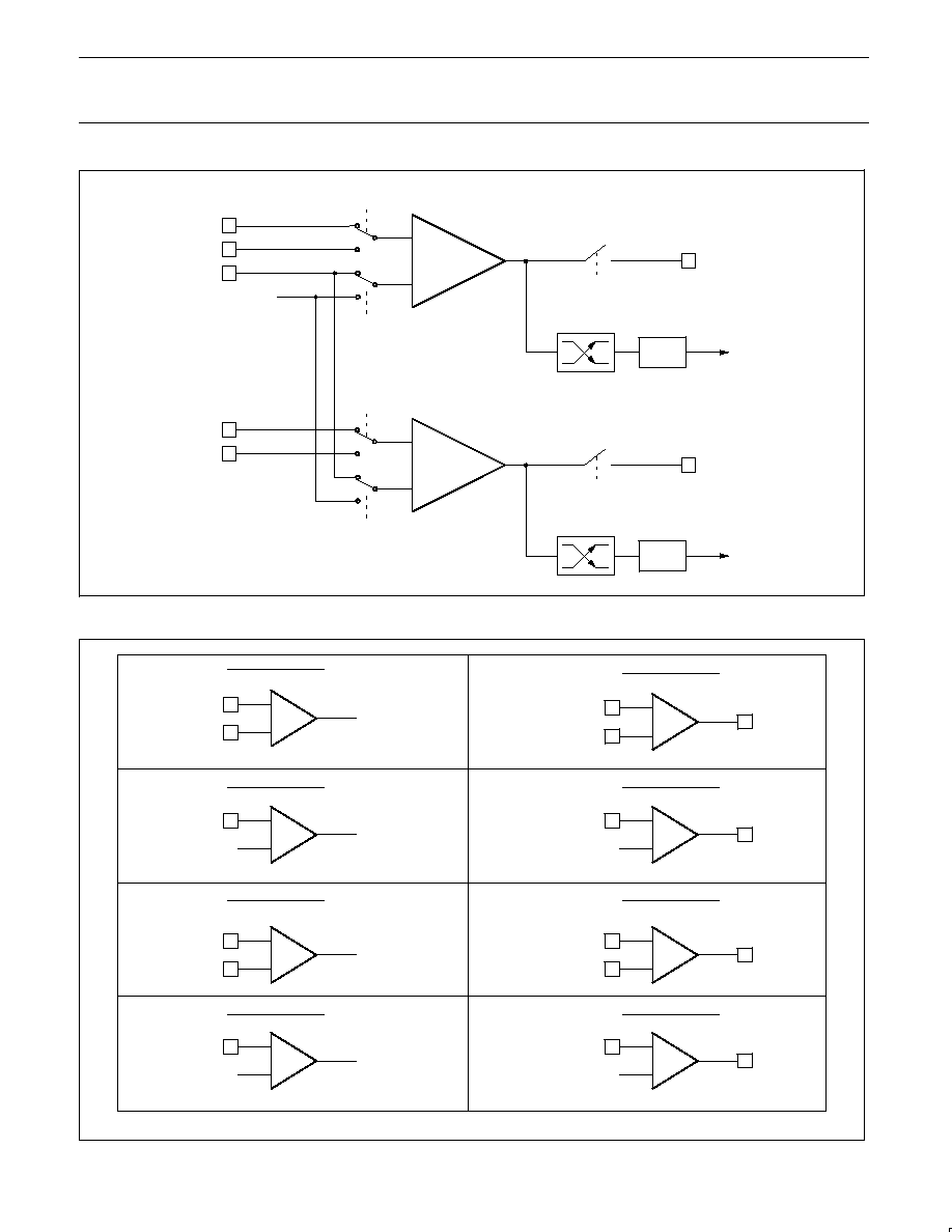
SU01153
+
≠
(P0.4) CIN1A
COMPARATOR 1
(P0.3) CIN1B
CO1
OE1
(P0.5) CMPREF
+
≠
(P0.2) CIN2A
COMPARATOR 2
(P0.1) CIN2B
CO2
OE2
CP1
CN1
CP2
CN2
CMP2 (P0.0)
CMP1 (P0.6)
CHANGE DETECT
CMF1
INTERRUPT
CHANGE DETECT
CMF2
INTERRUPT
V
ref
Figure 5. Comparator Input and Output Connections
V
ref
(1.23V)
V
ref
(1.23V)
V
ref
(1.23V)
SU01154
+
≠
CINnA
CMPREF
COn
CPn, CNn, OEn = 0 0 0
+
≠
CINnA
CMPREF
CMPn
COn
CPn, CNn, OEn = 0 0 1
+
≠
CINnA
CMPn
COn
CPn, CNn, OEn = 0 1 1
+
≠
CINnB
CMPREF
CMPn
COn
CPn, CNn, OEn = 1 0 1
+
≠
CINnB
CMPn
COn
CPn, CNn, OEn = 1 1 1
CPn, CNn, OEn = 0 1 0
CPn, CNn, OEn = 1 0 0
CPn, CNn, OEn = 1 1 0
+
≠
CINnA
Vref (1.23V)
COn
+
≠
CINnB
CMPREF
COn
+
≠
CINnB
COn
Figure 6. Comparator Configurations

Philips Semiconductors
Product data
87LPC767
Low power, low price, low pin count (20 pin)
microcontroller with 4-kbyte OTP and 8-bit A/D converter
2001 Aug 07
14
Internal Reference Voltage
An internal reference voltage generator may supply a default
reference when a single comparator input pin is used. The value of
the internal reference voltage, referred to as V
ref
, is 1.28 V
±
10%.
Comparator Interrupt
Each comparator has an interrupt flag CMFn contained in its
configuration register. This flag is set whenever the comparator
output changes state. The flag may be polled by software or may be
used to generate an interrupt. The interrupt will be generated when
the corresponding enable bit ECn in the IEN1 register is set and the
interrupt system is enabled via the EA bit in the IEN0 register.
Comparators and Power Reduction Modes
Either or both comparators may remain enabled when Power Down
or Idle mode is activated. The comparators will continue to function
in the power reduction mode. If a comparator interrupt is enabled, a
change of the comparator output state will generate an interrupt and
wake up the processor. If the comparator output to a pin is enabled,
the pin should be configured in the push-pull mode in order to obtain
fast switching times while in power down mode. The reason is that
with the oscillator stopped, the temporary strong pull-up that
normally occurs during switching on a quasi-bidirectional port pin
does not take place.
Comparators consume power in Power Down and Idle modes, as
well as in the normal operating mode. This fact should be taken into
account when system power consumption is an issue.
Comparator Configuration Example
The code shown in Figure 7 is an example of initializing one
comparator. Comparator 1 is configured to use the CIN1A and
CMPREF inputs, outputs the comparator result to the CMP1 pin,
and generates an interrupt when the comparator output changes.
The interrupt routine used for the comparator must clear the
interrupt flag (CMF1 in this case) before returning.
SU01189
CmpInit:
mov
PT0AD,#30h
; Disable digital inputs on pins that are used
; for analog functions: CIN1A, CMPREF.
anl
P0M2,#0cfh
; Disable digital outputs on pins that are used
orl
P0M1,#30h
; for analog functions: CIN1A, CMPREF.
mov
CMP1,#24h
; Turn on comparator 1 and set up for:
; ≠ Positive input on CIN1A.
; ≠ Negative input from CMPREF pin.
; ≠ Output to CMP1 pin enabled.
call
delay10us
; The comparator has to start up for at
; least 10 microseconds before use.
anl
CMP1,#0feh
; Clear comparator 1 interrupt flag.
setb
EC1
; Enable the comparator 1 interrupt. The
; priority is left at the current value.
setb
EA
; Enable the interrupt system (if needed).
ret
; Return to caller.
Figure 7.

Philips Semiconductors
Product data
87LPC767
Low power, low price, low pin count (20 pin)
microcontroller with 4-kbyte OTP and 8-bit A/D converter
2001 Aug 07
15
I
2
C Serial Interface
The I
2
C bus uses two wires (SDA and SCL) to transfer information
between devices connected to the bus. The main features of the
bus are:
∑
Bidirectional data transfer between masters and slaves.
∑
Serial addressing of slaves (no added wiring).
∑
Acknowledgment after each transferred byte.
∑
Multimaster bus.
∑
Arbitration between simultaneously transmitting masters without
corruption of serial data on bus.
The I
2
C subsystem includes hardware to simplify the software required
to drive the I
2
C bus. The hardware is a single bit interface which in
addition to including the necessary arbitration and framing error
checks, includes clock stretching and a bus timeout timer. The
interface is synchronized to software either through polled loops
or interrupts.
Refer to the application note AN422, entitled "Using the 8XC751
Microcontroller as an I
2
C Bus Master" for additional discussion of
the 8xC76x I
2
C interface and sample driver routines.
The 87LPC767 I2C implementation duplicates that of the 87C751
and 87C752 except for the following details:
∑
The interrupt vector addresses for both the I
2
C interrupt and the
Timer I interrupt.
∑
The I
2
C SFR addresses (I2CON, !2CFG, I2DAT).
∑
The location of the I
2
C interrupt enable bit and the name of the
SFR it is located within (EI2 is Bit 0 in IEN1).
∑
The location of the Timer I interrupt enable bit and the name of the
SFR it is located within (ETI is Bit 7 in IEN1).
∑
The I
2
C and Timer I interrupts have a settable priority.
Timer I is used to both control the timing of the I
2
C bus and also to
detect a "bus locked" condition, by causing an interrupt when
nothing happens on the I
2
C bus for an inordinately long period of
time while a transmission is in progress. If this interrupt occurs, the
program has the opportunity to attempt to correct the fault and
resume I
2
C operation.
Six time spans are important in I
2
C operation and are insured by timer I:
∑
The MINIMUM HIGH time for SCL when this device is the master.
∑
The MINIMUM LOW time for SCL when this device is a master.
This is not very important for a single-bit hardware interface like
this one, because the SCL low time is stretched until the software
responds to the I
2
C flags. The software response time normally
meets or exceeds the MIN LO time. In cases where the software
responds within MIN HI + MIN LO) time, timer I will ensure that
the minimum time is met.
∑
The MINIMUM SCL HIGH TO SDA HIGH time in a stop condition.
∑
The MINIMUM SDA HIGH TO SDA LOW time between I
2
C stop
and start conditions (4.7ms, see I
2
C specification).
∑
The MINIMUM SDA LOW TO SCL LOW time in a start condition.
∑
The MAXIMUM SCL CHANGE time while an I
2
C frame is in
progress. A frame is in progress between a start condition and the
following stop condition. This time span serves to detect a lack of
software response on this device as well as external I
2
C
problems. SCL "stuck low" indicates a faulty master or slave. SCL
"stuck high" may mean a faulty device, or that noise induced onto
the I
2
C bus caused all masters to withdraw from I
2
C arbitration.
The first five of these times are 4.7 ms (see I
2
C specification) and
are covered by the low order three bits of timer I. Timer I is clocked
by the 87LPC767 CPU clock. Timer I can be pre-loaded with one of
four values to optimize timing for different oscillator frequencies. At
lower frequencies, software response time is increased and will
degrade maximum performance of the I
2
C bus. See special function
register I2CFG description for prescale values (CT0, CT1).
The MAXIMUM SCL CHANGE time is important, but its exact span
is not critical. The complete 10 bits of timer I are used to count out
the maximum time. When I
2
C operation is enabled, this counter is
cleared by transitions on the SCL pin. The timer does not run
between I
2
C frames (i.e., whenever reset or stop occurred more
recently than the last start). When this counter is running, it will carry
out after 1020 to 1023 machine cycles have elapsed since a change
on SCL. A carry out causes a hardware reset of the I
2
C interface
and generates an interrupt if the Timer I interrupt is enabled. In
cases where the bus hang-up is due to a lack of software response
by this device, the reset releases SCL and allows I
2
C operation
among other devices to continue.
Timer I is enabled to run, and will reset the I
2
C interface upon
overflow, if the TIRUN bit in the I2CFG register is set. The Timer I
interrupt may be enabled via the ETI bit in IEN1, and its priority set
by the PTIH and PTI bits in the Ip1H and IP1 registers respectively.
I
2
C Interrupts
If I
2
C interrupts are enabled (EA and EI2 are both set to 1), an I
2
C
interrupt will occur whenever the ATN flag is set by a start, stop,
arbitration loss, or data ready condition (refer to the description of ATN
following). In practice, it is not efficient to operate the I
2
C interface in
this fashion because the I
2
C interrupt service routine would somehow
have to distinguish between hundreds of possible conditions. Also,
since I
2
C can operate at a fairly high rate, the software may execute
faster if the code simply waits for the I
2
C interface.
Typically, the I
2
C interrupt should only be used to indicate a start
condition at an idle slave device, or a stop condition at an idle master
device (if it is waiting to use the I
2
C bus). This is accomplished by
enabling the I
2
C interrupt only during the aforementioned conditions.
Reading I2CON
RDAT
The data from SDA is captured into "Receive DATa"
whenever a rising edge occurs on SCL. RDAT is also
available (with seven low-order zeros) in the I2DAT
register. The difference between reading it here and
there is that reading I2DAT clears DRDY, allowing the
I
2
C to proceed on to another bit. Typically, the first
seven bits of a received byte are read from
I2DAT, while the 8th is read here. Then I2DAT can be
written to send the Acknowledge bit and clear DRDY.
ATN
"ATteNtion" is 1 when one or more of DRDY, ARL, STR, or
STP is 1. Thus, ATN comprises a single bit that can be
tested to release the I
2
C service routine from a "wait loop."
DRDY
"Data ReaDY" (and thus ATN) is set when a rising edge
occurs on SCL, except at idle slave. DRDY is cleared
by writing CDR = 1, or by writing or reading the I2DAT
register. The following low period on SCL is stretched
until the program responds by clearing DRDY.

Philips Semiconductors
Product data
87LPC767
Low power, low price, low pin count (20 pin)
microcontroller with 4-kbyte OTP and 8-bit A/D converter
2001 Aug 07
16
BIT
SYMBOL
FUNCTION
I2CON.7
RDAT
Read: the most recently received data bit.
"
CXA
Write: clears the transmit active flag.
I2CON.6
ATN
Read: ATN = 1 if any of the flags DRDY, ARL, STP, or STP = 1.
"
IDLE
Write: in the I
2
C slave mode, writing a 1 to this bit causes the I
2
C hardware to ignore the bus until it
is needed again.
I2CON.5
DRDY
Read: Data Ready flag, set when there is a rising edge on SCL.
"
CDR
Write: writing a 1 to this bit clears the DRDY flag.
I2CON.4
ARL
Read: Arbitration Loss flag, set when arbitration is lost while in the transmit mode.
"
CARL
Write: writing a 1 to this bit clears the CARL flag.
I2CON.3
STR
Read: Start flag, set when a start condition is detected at a master or non-idle slave.
"
CSTR
Write: writing a 1 to this bit clears the STR flag.
I2CON.2
STP
Read: Stop flag, set when a stop condition is detected at a master or non-idle slave.
"
CSTP
Write: writing a 1 to this bit clears the STP flag.
I2CON.1
MASTER
Read: indicates whether this device is currently as bus master.
"
XSTR
Write: writing a 1 to this bit causes a repeated start condition to be generated.
I2CON.0
--
Read: undefined.
"
XSTP
Write: writing a 1 to this bit causes a stop condition to be generated.
* Due to the manner in which bit addressing is implemented in the 80C51 family, the I2CON register should never be altered by
use of the SETB, CLR, CPL, MOV (bit), or JBC instructions. This is due to the fact that read and write functions of this register
are different. Testing of I2CON bits via the JB and JNB instructions is supported.
--
SU01155
MASTER
STP
STR
ARL
DRDY
ATN
RDAT
0
1
2
3
4
5
6
7
I2CON
Reset Value: 81h
Bit Addressable*
Address: D8h
XSTP
XSTR
CSTP
CSTR
CARL
CDR
IDLE
CXA
READ
WRITE
Figure 8. I
2
C Control Register (I2CON)
BIT
SYMBOL
FUNCTION
I2DAT.7
RDAT
Read: the most recently received data bit, captured from SDA at every rising edge of SCL. Reading
I2DAT also clears DRDY and the Transmit Active state.
"
XDAT
Write: sets the data for the next transmitted bit. Writing I2DAT also clears DRDY and sets the
Transmit Active state.
I2DAT.6≠0
≠
Unused.
--
SU01156
--
--
--
--
--
--
RDAT
0
1
2
3
4
5
6
7
I2DAT
Reset Value: xxh
Not Bit Addressable
Address: D9h
--
--
--
--
--
--
--
XDAT
READ
WRITE
Figure 9. I
2
C Data Register (
I
2DAT)

Philips Semiconductors
Product data
87LPC767
Low power, low price, low pin count (20 pin)
microcontroller with 4-kbyte OTP and 8-bit A/D converter
2001 Aug 07
17
Checking ATN and DRDY
When a program detects ATN = 1, it should next check DRDY. If
DRDY = 1, then if it receives the last bit, it should capture the data
from RDAT (in I2DAT or I2CON). Next, if the next bit is to be sent, it
should be written to I2DAT. One way or another, it should clear
DRDY and then return to monitoring ATN. Note that if any of ARL,
STR, or STP is set, clearing DRDY will not release SCL to high, so
that the I
2
C will not go on to the next bit. If a program detects
ATN = 1, and DRDY = 0, it should go on to examine ARL, STR,
and STP.
ARL
"Arbitration Loss" is 1 when transmit Active was set, but
this device lost arbitration to another transmitter.
Transmit Active is cleared when ARL is 1. There are
four separate cases in which ARL is set.
1. If the program sent a 1 or repeated start, but another
device sent a 0, or a stop, so that SDA is 0 at the rising
edge of SCL. (If the other device sent a stop, the setting
of ARL will be followed shortly by STP being set.)
2. If the program sent a 1, but another device sent a
repeated start, and it drove SDA low before SCL
could be driven low. (This type of ARL is always
accompanied by STR = 1.)
3. In master mode, if the program sent a repeated start,
but another device sent a 1, and it drove SCL low
before this device could drive SDA low.
4. In master mode, if the program sent stop, but it could
not be sent because another device sent a 0.
STR
"STaRt" is set to a 1 when an I
2
C start condition is
detected at a non-idle slave or at a master. (STR is not
set when an idle slave becomes active due to a start
bit; the slave has nothing useful to do until the rising
edge of SCL sets DRDY.)
STP
"SToP" is set to 1 when an I
2
C stop condition is
detected at a non-idle slave or at a master. (STP is not
set for a stop condition at an idle slave.)
MASTER
"MASTER" is 1 if this device is currently a master on
the I
2
C. MASTER is set when MASTRQ is 1 and the
bus is not busy (i.e., if a start bit hasn't been
received since reset or a "Timer I" time-out, or if a stop
has been received since the last start). MASTER is
cleared when ARL is set, or after the software writes
MASTRQ = 0 and then XSTP = 1.
Writing I2CON
Typically, for each bit in an I
2
C message, a service routine waits for
ATN = 1. Based on DRDY, ARL, STR, and STP, and on the current
bit position in the message, it may then write I2CON with one or
more of the following bits, or it may read or write the I2DAT register.
CXA
Writing a 1 to "Clear Xmit Active" clears the Transmit
Active state. (Reading the I2DAT register also does this.)
Regarding Transmit Active
Transmit Active is set by writing the I2DAT register, or by writing
I2CON with XSTR = 1 or XSTP = 1. The I
2
C interface will only drive
the SDA line low when Transmit Active is set, and the ARL bit will
only be set to 1 when Transmit Active is set. Transmit Active is
cleared by reading the I2DAT register, or by writing I2CON with
CXA = 1. Transmit Active is automatically cleared when ARL is 1.
IDLE
Writing 1 to "IDLE" causes a slave's I
2
C hardware to
ignore the I
2
C until the next start condition (but if
MASTRQ is 1, then a stop condition will cause this
device to become a master).
CDR
Writing a 1 to "Clear Data Ready" clears DRDY.
(Reading or writing the I2DAT register also does this.)
CARL
Writing a 1 to "Clear Arbitration Loss" clears the ARL bit.
CSTR
Writing a 1 to "Clear STaRt" clears the STR bit.
CSTP
Writing a 1 to "Clear SToP" clears the STP bit. Note that
if one or more of DRDY, ARL, STR, or STP is 1, the low
time of SCL is stretched until the service routine
responds by clearing them.
XSTR
Writing 1s to "Xmit repeated STaRt" and CDR tells the
I
2
C hardware to send a repeated start condition. This
should only be at a master. Note that XSTR need not
and should not be used to send an "initial"
(non-repeated) start; it is sent automatically by the I
2
C
hardware. Writing XSTR = 1 includes the effect of
writing I2DAT with XDAT = 1; it sets Transmit Active
and releases SDA to high during the SCL low time.
After SCL goes high, the I
2
C hardware waits for the
suitable minimum time and then drives SDA low to
make the start condition.
XSTP
Writing 1s to "Xmit SToP" and CDR tells the I
2
C
hardware to send a stop condition. This should only be
done at a master. If there are no more messages to
initiate, the service routine should clear the MASTRQ
bit in I2CFG to 0 before writing XSTP with 1. Writing
XSTP = 1 includes the effect of writing I2DAT with
XDAT = 0; it sets Transmit Active and drives SDA low
during the SCL low time. After SCL goes high, the I
2
C
hardware waits for the suitable minimum time and then
releases SDA to high to make the stop condition.

Philips Semiconductors
Product data
87LPC767
Low power, low price, low pin count (20 pin)
microcontroller with 4-kbyte OTP and 8-bit A/D converter
2001 Aug 07
18
BIT
SYMBOL
FUNCTION
I2CFG.7
SLAVEN
Slave Enable. Writing a 1 this bit enables the slave functions of the I
2
C subsystem. If SLAVEN and
MASTRQ are 0, the I
2
C hardware is disabled. This bit is cleared to 0 by reset and by an I
2
C
time-out.
I2CFG.6
MASTRQ
Master Request. Writing a 1 to this bit requests mastership of the I
2
C bus. If a transmission is in
progress when this bit is changed from 0 to 1, action is delayed until a stop condition is detected. A
start condition is sent and DRDY is set (thus making ATN = 1 and generating an I
2
C interrupt).
When a master wishes to release mastership status of the I
2
C, it writes a 1 to XSTP in I2CON.
MASTRQ is cleared by an I
2
C time-out.
I2CFG.5
CLRTI
Writing a 1 to this bit clears the Timer I overflow flag. This bit position always reads as a 0.
I2CFG.4
TIRUN
Writing a 1 to this bit lets Timer I run; a zero stops and clears it. Together with SLAVEN, MASTRQ,
and MASTER, this bit determines operational modes as shown in Table 1.
I2CFG.2, 3
--
Reserved for future use. Should not be set to 1 by user programs.
I2CFG.1, 0 CT1, CT0
These two bits are programmed as a function of the CPU clock rate, to optimize the MIN HI and LO
time of SCL when this device is a master on the I
2
C. The time value determined by these bits
controls both of these parameters, and also the timing for stop and start conditions.
CT0
SU01157
CT1
--
--
TIRUN
CLRTI
MASTRQ
SLAVEN
0
1
2
3
4
5
6
7
I2CFG
Reset Value: 00h
Not Bit Addressable
Address: C8h
Figure 10. I
2
C Configuration Register (I2CFG)
Regarding Software Response Time
Because the 87LPC767 can run at 20 MHz, and because the I
2
C
interface is optimized for high-speed operation, it is quite likely that
an I
2
C service routine will sometimes respond to DRDY (which is set
at a rising edge of SCL) and write I2DAT before SCL has gone low
again. If XDAT were applied directly to SDA, this situation would
produce an I
2
C protocol violation. The programmer need not worry
about this possibility because XDAT is applied to SDA only when
SCL is low.
Conversely, a program that includes an I
2
C service routine may take
a long time to respond to DRDY. Typically, an I
2
C routine operates
on a flag-polling basis during a message, with interrupts from other
peripheral functions enabled. If an interrupt occurs, it will delay the
response of the I
2
C service routine. The programmer need not worry
about this very much either, because the I
2
C hardware stretches the
SCL low time until the service routine responds. The only constraint
on the response is that it must not exceed the Timer I time-out.
Values to be used in the CT1 and CT0 bits are shown in Table 2. To
allow the I
2
C bus to run at the maximum rate for a particular
oscillator frequency, compare the actual oscillator rate to the f
OSC
max column in the table. The value for CT1 and CT0 is found in the
first line of the table where CPU clock max is greater than or equal
to the actual frequency.
Table 2 also shows the machine cycle count for various settings of
CT1/CT0. This allows calculation of the actual minimum high and
low times for SCL as follows:
SCL min high low time (in microseconds)
+
6 * Min Time Count
CPU clock (in MHz)
For instance, at an 8 MHz frequency, with CT1/CT0 set to 1 0, the
minimum SCL high and low times will be 5.25
µ
s.
Table 2 also shows the Timer I timeout period (given in machine
cycles) for each CT1/CT0 combination. The timeout period varies
because of the way in which minimum SCL high and low times are
measured. When the I
2
C interface is operating, Timer I is pre-loaded
at every SCL transition with a value dependent upon CT1/CT0. The
pre-load value is chosen such that a minimum SCL high or low time
has elapsed when Timer I reaches a count of 008 (the actual value
pre-loaded into Timer I is 8 minus the machine cycle count).
Philips Semiconductors
Product data
87LPC767
Low power, low price, low pin count (20 pin)
microcontroller with 4-kbyte OTP and 8-bit A/D converter
2001 Aug 07
19
Table 1. Interaction of TIRUN with SLAVEN, MASTRQ, and MASTER
SLAVEN,
MASTRQ,
MASTER
TIRUN
OPERATING MODE
All 0
0
The I
2
C interface is disabled. Timer I is cleared and does not run. This is the state assumed after a reset. If an I
2
C
application wants to ignore the I
2
C at certain times, it should write SLAVEN, MASTRQ, and TIRUN all to zero.
All 0
1
The I
2
C interface is disabled.
Any or all 1
0
The I
2
C interface is enabled. The 3 low-order bits of Timer I run for min-time generation, but the hi-order bits do
not, so that there is no checking for I
2
C being "hung." This configuration can be used for very slow I
2
C operation.
Any or all 1
1
The I
2
C interface is enabled. Timer I runs during frames on the I
2
C, and is cleared by transitions on SCL, and by
Start and Stop conditions. This is the normal state for I
2
C operation.
Table 2. CT1, CT0 Values
CT1, CT0
Min Time Count
(Machine Cycles)
CPU Clock Max
(for 100 kHz I
2
C)
Timeout Period
(Machine Cycles)
1 0
7
8.4 MHz
1023
0 1
6
7.2 MHz
1022
0 0
5
6.0 MHz
1021
1 1
4
4.8 MHz
1020
Interrupts
The 87LPC767 uses a four priority level interrupt structure. This
allows great flexibility in controlling the handling of the 87LPC767's many
interrupt sources. The 87LPC767 supports up to 13 interrupt sources.
Each interrupt source can be individually enabled or disabled by
setting or clearing a bit in registers IEN0 or IEN1. The IEN0
register also contains a global disable bit, EA, which disables all
interrupts at once.
Each interrupt source can be individually programmed to one of four
priority levels by setting or clearing bits in the IP0, IP0H, IP1, and
IP1H registers. An interrupt service routine in progress can be
interrupted by a higher priority interrupt, but not by another interrupt
of the same or lower priority. The highest priority interrupt service
cannot be interrupted by any other interrupt source. So, if two
requests of different priority levels are received simultaneously, the
request of higher priority level is serviced.
If requests of the same priority level are received simultaneously, an
internal polling sequence determines which request is serviced. This
is called the arbitration ranking. Note that the arbitration ranking is
only used to resolve simultaneous requests of the same priority level.
Table 3 summarizes the interrupt sources, flag bits, vector
addresses, enable bits, priority bits, arbitration ranking, and whether
each interrupt may wake up the CPU from Power Down mode.
Table 3. Summary of Interrupts
Description
Interrupt
Flag Bit(s)
Vector
Address
Interrupt
Enable Bit(s)
Interrupt
Priority
Arbitration
Ranking
Power Down
Wakeup
External Interrupt 0
IE0
0003h
EX0 (IEN0.0)
IP0H.0, IP0.0
1 (highest)
Yes
Timer 0 Interrupt
TF0
000Bh
ET0 (IEN0.1)
IP0H.1, IP0.1
4
No
External Interrupt 1
IE1
0013h
EX1 (IEN0.2)
IP0H.2, IP0.2
7
Yes
Timer 1 Interrupt
TF1
001Bh
ET1 (IEN0.3)
IP0H.3, IP0.3
10
No
Serial Port Tx and Rx
TI & RI
0023h
ES (IEN0.4)
IP0H.4, IP0.4
12
No
Brownout Detect
BOD
002Bh
EBO (IEN0.5)
IP0H.5, IP0.5
2
Yes
I
2
C Interrupt
ATN
0033h
EI2 (IEN1.0)
IP1H.0, IP1.0
5
No
KBI Interrupt
KBF
003Bh
EKB (IEN1.1)
IP1H.1, IP1.1
8
Yes
Comparator 2 interrupt
CMF2
0043h
EC2 (IEN1.2)
IP1H.2, IP1.2
11
Yes
Watchdog Timer
WDOVF
0053h
EWD (IEN0.6)
IP0H.6, IP0.6
3
Yes
A/D Converter
ADCI
005Bh
EAD (IEN1.4)
IP1H.4, IP1.4
6
Yes
Comparator 1 interrupt
CMF1
0063h
EC1 (IEN1.5)
IP1H.5, IP1.5
9
Yes
Timer I
≠
0073h
ETI (IEN1.7)
IP1H.7, IP1.7
13 (lowest)
No
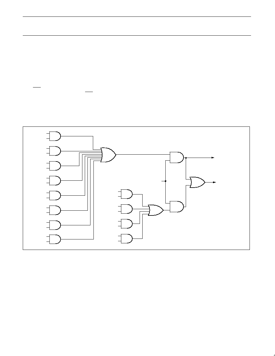
Philips Semiconductors
Product data
87LPC767
Low power, low price, low pin count (20 pin)
microcontroller with 4-kbyte OTP and 8-bit A/D converter
2001 Aug 07
20
External Interrupt Inputs
The 87LPC767 has two individual interrupt inputs as well as the
Keyboard Interrupt function. The latter is described separately
elsewhere in this section. The two interrupt inputs are identical to
those present on the standard 80C51 microcontroller.
The external sources can be programmed to be level-activated or
transition-activated by setting or clearing bit IT1 or IT0 in Register
TCON. If ITn = 0, external interrupt n is triggered by a detected low
at the INTn pin. If ITn = 1, external interrupt n is edge triggered. In
this mode if successive samples of the INTn pin show a high in one
cycle and a low in the next cycle, interrupt request flag IEn in TCON
is set, causing an interrupt request.
Since the external interrupt pins are sampled once each machine
cycle, an input high or low should hold for at least 6 CPU Clocks to
ensure proper sampling. If the external interrupt is
transition-activated, the external source has to hold the request pin
high for at least one machine cycle, and then hold it low for at least
one machine cycle. This is to ensure that the transition is seen and
that interrupt request flag IEn is set. IEn is automatically cleared by
the CPU when the service routine is called.
If the external interrupt is level-activated, the external source must
hold the request active until the requested interrupt is actually
generated. If the external interrupt is still asserted when the interrupt
service routine is completed another interrupt will be generated. It is
not necessary to clear the interrupt flag IEn when the interrupt is
level sensitive, it simply tracks the input pin level.
If an external interrupt is enabled when the 87LPC767 is put into
Power Down or Idle mode, the interrupt will cause the processor to
wake up and resume operation. Refer to the section on Power
Reduction Modes for details.
SU01353
WAKEUP
(IF IN POWER
DOWN)
EA
(FROM IEN0
REGISTER)
INTERRUPT
TO CPU
IE0
EX0
IE1
EX1
BOD
EBO
KBF
EKB
CM2
EC2
WDT
EWD
ADC
EAD
TF0
ET0
TF1
ET1
RI + TI
ES
ATN
EI2
CM1
EC1
Figure 11. Interrupt Sources, Interrupt Enables, and Power Down Wakeup Sources
Philips Semiconductors
Product data
87LPC767
Low power, low price, low pin count (20 pin)
microcontroller with 4-kbyte OTP and 8-bit A/D converter
2001 Aug 07
21
I/O Ports
The 87LPC767 has 3 I/O ports, port 0, port 1, and port 2. The exact
number of I/O pins available depend upon the oscillator and reset
options chosen. At least 15 pins of the 87LPC767 may be used as
I/Os when a two-pin external oscillator and an external reset circuit
are used. Up to 18 pins may be available if fully on-chip oscillator
and reset configurations are chosen.
All but three I/O port pins on the 87LPC767 may be software
configured to one of four types on a bit-by-bit basis, as shown in
Table 4. These are: quasi-bidirectional (standard 80C51 port
outputs), push-pull, open drain, and input only. Two configuration
registers for each port choose the output type for each port pin.
Table 4. Port Output Configuration Settings
PxM1.y
PxM2.y
Port Output Mode
0
0
Quasi-bidirectional
0
1
Push-Pull
1
0
Input Only (High Impedance)
1
1
Open Drain
Quasi-Bidirectional Output
Configuration
The default port output configuration for standard 87LPC767 I/O
ports is the quasi-bidirectional output that is common on the 80C51
and most of its derivatives. This output type can be used as both an
input and output without the need to reconfigure the port. This is
possible because when the port outputs a logic high, it is weakly
driven, allowing an external device to pull the pin low. When the pin
is pulled low, it is driven strongly and able to sink a fairly large
current. These features are somewhat similar to an open drain
output except that there are three pull-up transistors in the
quasi-bidirectional output that serve different purposes.
One of these pull-ups, called the "very weak" pull-up, is turned on
whenever the port latch for the pin contains a logic 1. The very weak
pull-up sources a very small current that will pull the pin high if it is
left floating.
A second pull-up, called the "weak" pull-up, is turned on when the
port latch for the pin contains a logic 1 and the pin itself is also at a
logic 1 level. This pull-up provides the primary source current for a
quasi-bidirectional pin that is outputting a 1. If a pin that has a logic 1
on it is pulled low by an external device, the weak pull-up turns off,
and only the very weak pull-up remains on. In order to pull the pin
low under these conditions, the external device has to sink enough
current to overpower the weak pull-up and take the voltage on the
port pin below its input threshold.
The third pull-up is referred to as the "strong" pull-up. This pull-up is
used to speed up low-to-high transitions on a quasi-bidirectional port
pin when the port latch changes from a logic 0 to a logic 1. When this
occurs, the strong pull-up turns on for a brief time, two CPU clocks, in
order to pull the port pin high quickly. Then it turns off again.
The quasi-bidirectional port configuration is shown in Figure 12.
SU01159
WEAK
VERY
WEAK
STRONG
PORT
PIN
V
DD
2 CPU
CLOCK DELAY
INPUT
DATA
PORT LATCH
DATA
N
P
P
P
Figure 12. Quasi-Bidirectional Output
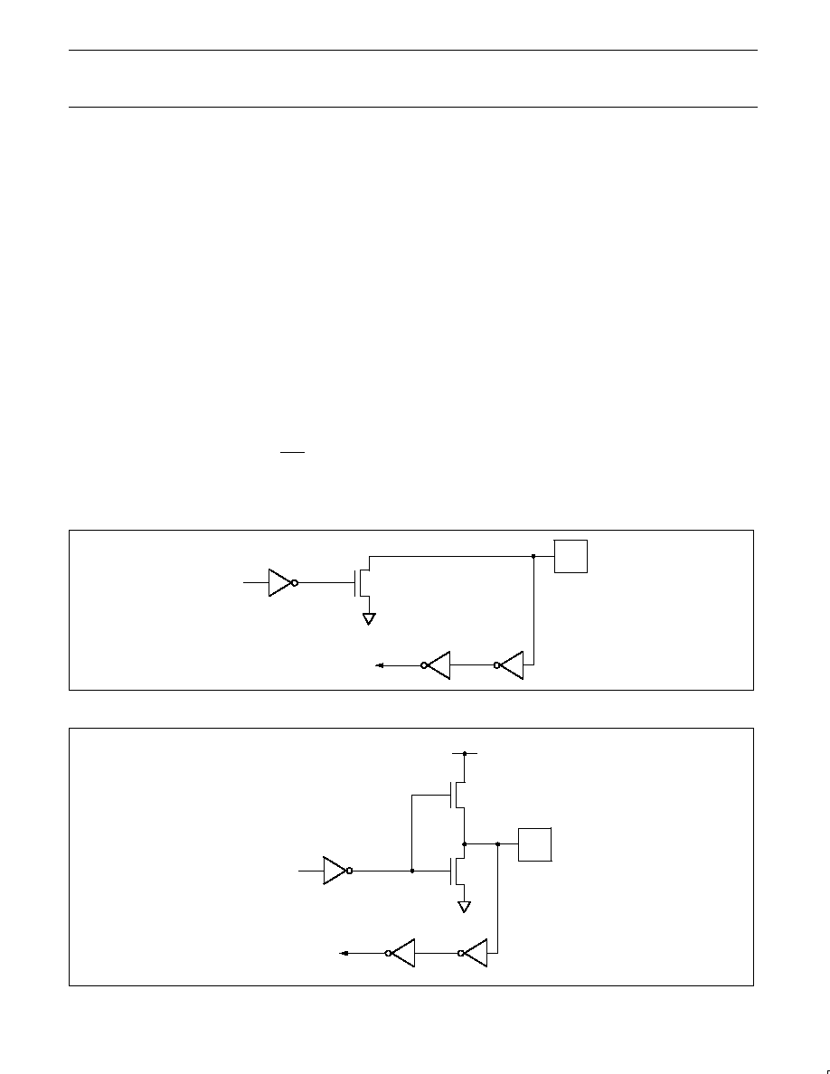
Philips Semiconductors
Product data
87LPC767
Low power, low price, low pin count (20 pin)
microcontroller with 4-kbyte OTP and 8-bit A/D converter
2001 Aug 07
22
Open Drain Output
Configuration
The open drain output configuration turns off all pull-ups and only
drives the pull-down transistor of the port driver when the port latch
contains a logic 0. To be used as a logic output, a port configured in
this manner must have an external pull-up, typically a resistor tied to
V
DD
. The pull-down for this mode is the same as for the
quasi-bidirectional mode.
The open drain port configuration is shown in Figure 13.
Push-Pull Output
Configuration
The push-pull output configuration has the same pull-down structure
as both the open drain and the quasi-bidirectional output modes, but
provides a continuous strong pull-up when the port latch contains a
logic 1. The push-pull mode may be used when more source current
is needed from a port output.
The push-pull port configuration is shown in Figure 14.
The three port pins that cannot be configured are P1.2, P1.3, and
P1.5. The port pins P1.2 and P1.3 are permanently configured as
open drain outputs. They may be used as inputs by writing ones to
their respective port latches. P1.5 may be used as a Schmitt trigger
input if the 87LPC767 has been configured for an internal reset and
is not using the external reset input function RST.
Additionally, port pins P2.0 and P2.1 are disabled for both input and
output if one of the crystal oscillator options is chosen. Those
options are described in the Oscillator section.
The value of port pins at reset is determined by the PRHI bit in the
UCFG1 register. Ports may be configured to reset high or low as
needed for the application. When port pins are driven high at reset,
they are in quasi-bidirectional mode and therefore do not source
large amounts of current.
Every output on the 87LPC767 may potentially be used as a 20 mA
sink LED drive output. However, there is a maximum total output
current for all ports which must not be exceeded.
All ports pins of the 87LPC767 have slew rate controlled outputs. This
is to limit noise generated by quickly switching output signals. The
slew rate is factory set to approximately 10 ns rise and fall times.
The bits in the P2M1 register that are not used to control
configuration of P2.1 and P2.0 are used for other purposes. These
bits can enable Schmitt trigger inputs on each I/O port, enable
toggle outputs from Timer 0 and Timer 1, and enable a clock output
if either the internal RC oscillator or external clock input is being
used. The last two functions are described in the Timer/Counters
and Oscillator sections respectively. The enable bits for all of these
functions are shown in Figure 15.
Each I/O port of the 87LPC767 may be selected to use TTL level
inputs or Schmitt inputs with hysteresis. A single configuration bit
determines this selection for the entire port. Port pins P1.2, P1.3,
and P1.5 always have a Schmitt trigger input.
SU01160
PORT
PIN
INPUT
DATA
PORT LATCH
DATA
N
Figure 13. Open Drain Output
SU01161
PORT
PIN
V
DD
INPUT
DATA
PORT LATCH
DATA
N
P
Figure 14. Push-Pull Output

Philips Semiconductors
Product data
87LPC767
Low power, low price, low pin count (20 pin)
microcontroller with 4-kbyte OTP and 8-bit A/D converter
2001 Aug 07
23
BIT
SYMBOL
FUNCTION
P2M1.7
P2S
When P2S = 1, this bit enables Schmitt trigger inputs on Port 2.
P2M1.6
P1S
When P1S = 1, this bit enables Schmitt trigger inputs on Port 1.
P2M1.5
P0S
When P0S = 1, this bit enables Schmitt trigger inputs on Port 0.
P2M1.4
ENCLK
When ENCLK is set and the 87LPC764 is configured to use the on-chip RC oscillator, a clock
output is enabled on the X2 pin (P2.0). Refer to the Oscillator section for details.
P2M1.3
ENT1
When set, the P.7 pin is toggled whenever Timer 1 overflows. The output frequency is therefore
one half of the Timer 1 overflow rate. Refer to the Timer/Counters section for details.
P2M1.2
ENT0
When set, the P1.2 pin is toggled whenever Timer 0 overflows. The output frequency is therefore
one half of the Timer 0 overflow rate. Refer to the Timer/Counterssection for details.
P2M1.1, P2M1.0
--
These bits, along with the matching bits in the P2M2 register, control the output configuration of
P2.1 and P2.0 respectively, as shown in Table 4.
(P2M1.0)
SU01162
(P2M1.1)
ENT0
ENT1
ENCLK
P0S
P1S
P2S
0
1
2
3
4
5
6
7
P2M1
Reset Value: 00h
Not Bit Addressable
Address: A4h
Figure 15. Port 2 Mode Register 1 (P2M1)
Keyboard Interrupt (KBI)
The Keyboard Interrupt function is intended primarily to allow a
single interrupt to be generated when any key is pressed on a
keyboard or keypad connected to specific pins of the 87LPC767, as
shown in Figure 16. This interrupt may be used to wake up the CPU
from Idle or Power Down modes. This feature is particularly useful in
handheld, battery powered systems that need to carefully manage
power consumption yet also need to be convenient to use.
The 87LPC767 allows any or all pins of port 0 to be enabled to
cause this interrupt. Port pins are enabled by the setting of bits in
the KBI register, as shown in Figure 17. The Keyboard Interrupt Flag
(KBF) in the AUXR1 register is set when any enabled pin is pulled
low while the KBI interrupt function is active. An interrupt will
generated if it has been enabled. Note that the KBF bit must be
cleared by software.
Due to human time scales and the mechanical delay associated with
keyswitch closures, the KBI feature will typically allow the interrupt
service routine to poll port 0 in order to determine which key was
pressed, even if the processor has to wake up from Power Down
mode. Refer to the section on Power Reduction Modes for details.

Philips Semiconductors
Product data
87LPC767
Low power, low price, low pin count (20 pin)
microcontroller with 4-kbyte OTP and 8-bit A/D converter
2001 Aug 07
24
SU01163
KBF (KBI INTERRUPT)
EKB
(FROM IEN1 REGISTER)
P0.7
KBI.7
P0.6
KBI.6
P0.5
P0.4
P0.3
P0.2
P0.1
P0.0
KBI.5
KBI.4
KBI.3
KBI.2
KBI.1
KBI.0
Figure 16. Keyboard Interrupt
BIT
SYMBOL
FUNCTION
KBI.7
--
When set, enables P0.7 as a cause of a Keyboard Interrupt.
KBI.6
--
When set, enables P0.6 as a cause of a Keyboard Interrupt.
KBI.5
--
When set, enables P0.5 as a cause of a Keyboard Interrupt.
KBI.4
--
When set, enables P0.4 as a cause of a Keyboard Interrupt.
KBI.3
--
When set, enables P0.3 as a cause of a Keyboard Interrupt.
KBI.2
--
When set, enables P0.2 as a cause of a Keyboard Interrupt.
KBI.1
--
When set, enables P0.1 as a cause of a Keyboard Interrupt.
KBI.0
--
When set, enables P0.0 as a cause of a Keyboard Interrupt.
Note: the Keyboard Interrupt must be enabled in order for the settings of the KBI register to be effective. The interrupt flag
(KBF) is located at bit 7 of AUXR1.
KBI.0
SU01164
KBI.1
KBI.2
KBI.3
KBI.4
KBI.5
KBI.6
KBI.7
0
1
2
3
4
5
6
7
KBI
Reset Value: 00h
Not Bit Addressable
Address: 86h
Figure 17. Keyboard Interrupt Register (KBI)
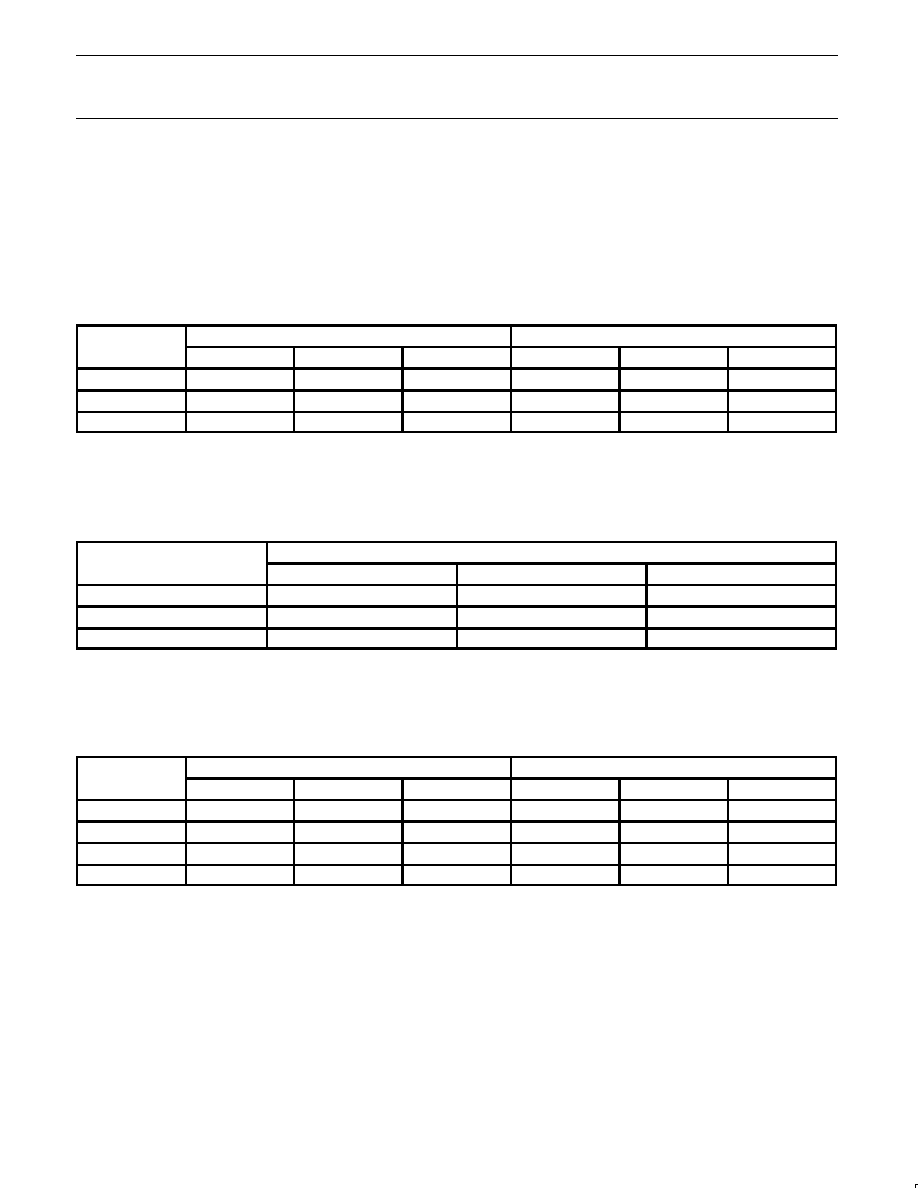
Philips Semiconductors
Product data
87LPC767
Low power, low price, low pin count (20 pin)
microcontroller with 4-kbyte OTP and 8-bit A/D converter
2001 Aug 07
25
Oscillator
The 87LPC767 provides several user selectable oscillator options,
allowing optimization for a range of needs from high precision to
lowest possible cost. These are configured when the EPROM is
programmed. Basic oscillator types that are supported include: low,
medium, and high speed crystals, covering a range from 20 kHz to
20 MHz; ceramic resonators; and on-chip RC oscillator.
Low Frequency Oscillator Option
This option supports an external crystal in the range of 20 kHz to 100 kHz.
Table 5 shows capacitor values that may be used with a quartz crystal in this mode.
Table 5. Recommended oscillator capacitors for use with the low frequency oscillator option
Oscillator
V
DD
= 2.7 to 4.5 V
V
DD
= 4.5 to 6.0 V
Frequency
Lower Limit
Optimal Value
Upper Limit
Lower Limit
Optimal Value
Upper Limit
20 kHz
15 pF
15 pF
33 pF
33 pF
33 pF
47 pF
32 kHz
15 pF
15 pF
33 pF
33 pF
33 pF
47 pF
100 kHz
15 pF
15 pF
33 pF
15 pF
15 pF
33 pF
Medium Frequency Oscillator Option
This option supports an external crystal in the range of 100 kHz to 4 MHz. Ceramic resonators are also supported in this configuration.
Table 6 shows capacitor values that may be used with a quartz crystal in this mode.
Table 6. Recommended oscillator capacitors for use with the medium frequency oscillator option
Oscillator Freq ency
V
DD
= 2.7 to 4.5 V
Oscillator Frequency
Lower Limit
Optimal Value
Upper Limit
100 kHz
33 pF
33 pF
47 pF
1 MHz
15 pF
15 pF
33 pF
4 MHz
15 pF
15 pF
33 pF
High Frequency Oscillator Option
This option supports an external crystal in the range of 4 to 20 MHz. Ceramic resonators are also supported in this configuration.
Table 7 shows capacitor values that may be used with a quartz crystal in this mode.
Table 7. Recommended oscillator capacitors for use with the high frequency oscillator option
Oscillator
V
DD
= 2.7 to 4.5 V
V
DD
= 4.5 to 6.0 V
Frequency
Lower Limit
Optimal Value
Upper Limit
Lower Limit
Optimal Value
Upper Limit
4 MHz
15 pF
33 pF
47 pF
15 pF
33 pF
68 pF
8 MHz
15 pF
15 pF
33 pF
15 pF
33 pF
47 pF
16 MHz
≠
≠
≠
15 pF
15 pF
33 pF
20 MHz
≠
≠
≠
15 pF
15 pF
33 pF
On-Chip RC Oscillator Option
The on-chip RC oscillator option has a typical frequency of 6 MHz
and can be divided down for slower operation through the use of the
DIVM register. Note that the on-chip oscillator has a
±
25% frequency
tolerance and for that reason may not be suitable for use in some
applications. A clock output on the X2/P2.0 pin may be enabled
when the on-chip RC oscillator is used.
External Clock Input Option
In this configuration, the processor clock is input from an external
source driving the X1/P2.1 pin. The rate may be from 0 Hz up to
20 MHz when V
DD
is above 4.5 V and up to 10 MHz when V
DD
is
below 4.5 V. When the external clock input mode is used, the X2/P2.0
pin may be used as a standard port pin. A clock output on the X2/P2.0
pin may be enabled when the external clock input is used.
Clock Output
The 87LPC767 supports a clock output function when either the
on-chip RC oscillator or external clock input options are selected.
This allows external devices to synchronize to the 87LPC767. When
enabled, via the ENCLK bit in the P2M1 register, the clock output
appears on the X2/CLKOUT pin whenever the on-chip oscillator is
running, including in Idle mode. The frequency of the clock output is
1/6 of the CPU clock rate. If the clock output is not needed in Idle
mode, it may be turned off prior to entering Idle, saving additional
power. The clock output may also be enabled when the external
clock input option is selected.
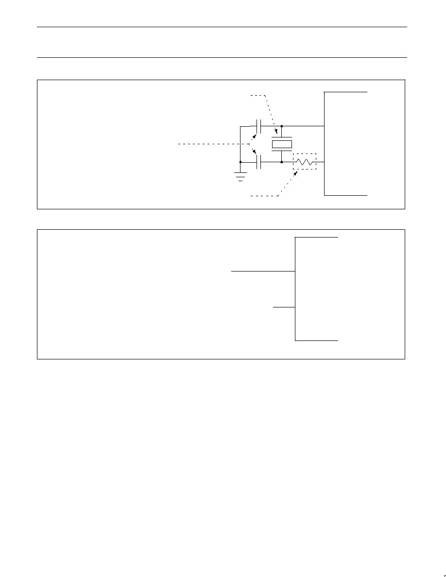
Philips Semiconductors
Product data
87LPC767
Low power, low price, low pin count (20 pin)
microcontroller with 4-kbyte OTP and 8-bit A/D converter
2001 Aug 07
26
SU01357
87LPC767
QUARTZ CRYSTAL OR
CERAMIC RESONATOR
X2
X1
THE OSCILLATOR MUST BE CONFIGURED IN ONE OF
THE FOLLOWING MODES:
≠ LOW FREQUENCY CRYSTAL
≠ MEDIUM FREQUENCY CRYSTAL
≠ HIGH FREQUENCY CRYSTAL
*
CAPACITOR VALUES MAY BE OPTIMIZED FOR
DIFFERENT OSCILLATOR FREQUENCIES (SEE TEXT)
A SERIES RESISTOR MAY BE REQUIRED IN ORDER TO
LIMIT CRYSTAL DRIVE LEVELS. THIS IS PARTICULARLY
IMPORTANT FOR LOW FREQUENCY CRYSTALS (SEE TEXT).
Figure 18. Using the Crystal Oscillator
SU01358
87LPC767
X2
X1
THE OSCILLATOR MUST BE CONFIGURED IN
THE EXTERNAL CLOCK INPUT MODE.
A CLOCK OUTPUT MAY BE OBTAINED ON
THE X2 PIN BY SETTING THE ENCLK BIT IN
THE P2M1 REGISTER.
CMOS COMPATIBLE EXTERNAL
OSCILLATOR SIGNAL
Figure 19. Using an External Clock Input
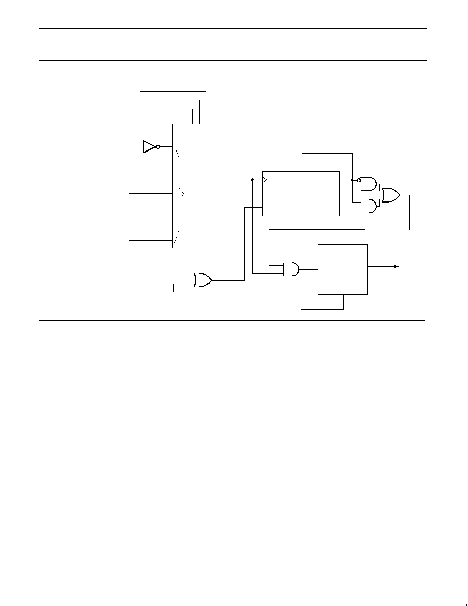
Philips Semiconductors
Product data
87LPC767
Low power, low price, low pin count (20 pin)
microcontroller with 4-kbyte OTP and 8-bit A/D converter
2001 Aug 07
27
SU01167
CLOCK SELECT
CLOCK
SOURCES
CLOCK
OUT
XTAL
SELECT
INTERNAL RC OSCILLATOR
CRYSTAL: LOW FREQUENCY
CRYSTAL: MEDIUM FREQUENCY
CRYSTAL: HIGH FREQUENCY
EXTERNAL CLOCK INPUT
10-BIT RIPPLE COUNTER
RESET
COUNT
COUNT 256
COUNT 1024
OSCILLATOR STARTUP TIMER
DIVIDE-BY-M
(DIVM REGISTER)
AND
CLKR SELECT
CPU
CLOCK
˜
1/
˜
2
CLKR
(UCFG1.3)
POWER DOWN
POWER MONITOR RESET
FOSC0 (UCFG1.0)
FOSC1 (UCFG1.1)
FOSC2 (UCFG1.2)
Figure 20. Block Diagram of Oscillator Control
CPU Clock Modification: CLKR and DIVM
For backward compatibility, the CLKR configuration bit allows
setting the 87LPC767 instruction and peripheral timing to match
standard 80C51 timing by dividing the CPU clock by two. Default
timing for the 87LPC767 is 6 CPU clocks per machine cycle while
standard 80C51 timing is 12 clocks per machine cycle. This
division also applies to peripheral timing, allowing 80C51 code that
is oscillator frequency and/or timer rate dependent. The CLKR bit
is located in the EPROM configuration register UCFG1, described
under EPROM Characteristics
In addition to this, the CPU clock may be divided down from the
oscillator rate by a programmable divider, under program control.
This function is controlled by the DIVM register. If the DIVM register
is set to zero (the default value), the CPU will be clocked by either
the unmodified oscillator rate, or that rate divided by two, as
determined by the previously described CLKR function.
When the DIVM register is set to some value N (between 1 and 255),
the CPU clock is divided by 2 * (N + 1). Clock division values from 4
through 512 are thus possible. This feature makes it possible to
temporarily run the CPU at a lower rate, reducing power consumption,
in a manner similar to Idle mode. By dividing the clock, the CPU can
retain the ability to respond to events other than those that can cause
interrupts (i.e., events that allow exiting the Idle mode) by executing
its normal program at a lower rate. This can allow bypassing the
oscillator startup time in cases where Power Down mode would
otherwise be used. The value of DIVM may be changed by the
program at any time without interrupting code execution.
Power Monitoring Functions
The 87LPC767 incorporates power monitoring functions designed to
prevent incorrect operation during initial power up and power loss or
reduction during operation. This is accomplished with two hardware
functions: Power-On Detect and Brownout Detect.
Brownout Detection
The Brownout Detect function allows preventing the processor from
failing in an unpredictable manner if the power supply voltage drops
below a certain level. The default operation is for a brownout
detection to cause a processor reset, however it may alternatively
be configured to generate an interrupt by setting the BOI bit in the
AUXR1 register (AUXR1.5).
The 87LPC767 allows selection of two Brownout levels: 2.5 V or
3.8 V. When V
DD
drops below the selected voltage, the brownout
detector triggers and remains active until V
DD
is returns to a level
above the Brownout Detect voltage. When Brownout Detect causes
a processor reset, that reset remains active as long as V
DD
remains
below the Brownout Detect voltage. When Brownout Detect
generates an interrupt, that interrupt occurs once as V
DD
crosses
from above to below the Brownout Detect voltage. For the interrupt
to be processed, the interrupt system and the BOI interrupt must
both be enabled (via the EA and EBO bits in IEN0).
When Brownout Detect is activated, the BOF flag in the PCON
register is set so that the cause of processor reset may be determined
by software. This flag will remain set until cleared by software.

Philips Semiconductors
Product data
87LPC767
Low power, low price, low pin count (20 pin)
microcontroller with 4-kbyte OTP and 8-bit A/D converter
2001 Aug 07
28
For correct activation of Brownout Detect, the V
DD
fall time must be
no faster than 50 mV/
µ
s. When V
DD
is restored, is should not rise
faster than 2 mV/
µ
s in order to insure a proper reset.
The brownout voltage (2.5 V or 3.8 V) is selected via the BOV bit in
the EPROM configuration register UCFG1. When unprogrammed
(BOV = 1), the brownout detect voltage is 2.5 V. When programmed
(BOV = 0), the brownout detect voltage is 3.8 V.
If the Brownout Detect function is not required in an application, it
may be disabled, thus saving power. Brownout Detect is disabled by
setting the control bit BOD in the AUXR1 register (AUXR1.6).
Power On Detection
The Power On Detect has a function similar to the Brownout Detect,
but is designed to work as power comes up initially, before the
power supply voltage reaches a level where Brownout Detect can
work. When this feature is activated, the POF flag in the PCON
register is set to indicate an initial power up condition. The POF flag
will remain set until cleared by software.
Power Reduction Modes
The 87LPC767 supports Idle and Power Down modes of power
reduction.
Idle Mode
The Idle mode leaves peripherals running in order to allow them to
activate the processor when an interrupt is generated. Any enabled
interrupt source or Reset may terminate Idle mode. Idle mode is
entered by setting the IDL bit in the PCON register (see Figure 21).
Power Down Mode
The Power Down mode stops the oscillator in order to absolutely
minimize power consumption. Power Down mode is entered by
setting the PD bit in the PCON register (see Figure 21).
The processor can be made to exit Power Down mode via Reset or
one of the interrupt sources shown in Table 5. This will occur if the
interrupt is enabled and its priority is higher than any interrupt
currently in progress.
In Power Down mode, the power supply voltage may be reduced to
the RAM keep-alive voltage V
RAM
. This retains the RAM contents
at the point where Power Down mode was entered. SFR contents
are not guaranteed after V
DD
has been lowered to V
RAM
, therefore
it is recommended to wake up the processor via Reset in this case.
V
DD
must be raised to within the operating range before the Power
Down mode is exited. Since the watchdog timer has a separate
oscillator, it may reset the processor upon overflow if it is running
during Power Down.
Note that if the Brownout Detect reset is enabled, the processor will
be put into reset as soon as V
DD
drops below the brownout voltage.
If Brownout Detect is configured as an interrupt and is enabled, it will
wake up the processor from Power Down mode when V
DD
drops
below the brownout voltage.
When the processor wakes up from Power Down mode, it will start
the oscillator immediately and begin execution when the oscillator is
stable. Oscillator stability is determined by counting 1024 CPU
clocks after start-up when one of the crystal oscillator configurations
is used, or 256 clocks after start-up for the internal RC or external
clock input configurations.
Some chip functions continue to operate and draw power during
Power Down mode, increasing the total power used during Power
Down. These include the Brownout Detect, Watchdog Timer,
Comparators, and A/D converter.
BIT
SYMBOL
FUNCTION
PCON.7
SMOD1
When set, this bit doubles the UART baud rate for modes 1, 2, and 3.
PCON.6
SMOD0
This bit selects the function of bit 7 of the SCON SFR. When 0, SCON.7 is the SM0 bit. When 1,
SCON.7 is the FE (Framing Error) flag. See Figure 26 for additional information.
PCON.5
BOF
Brown Out Flag. Set automatically when a brownout reset or interrupt has occurred. Also set at
power on. Cleared by software. Refer to the Power Monitoring Functions section for additional
information.
PCON.4
POF
Power On Flag. Set automatically when a power-on reset has occurred. Cleared by software. Refer
to the Power Monitoring Functions section for additional information.
PCON.3
GF1
General purpose flag 1. May be read or written by user software, but has no effect on operation.
PCON.2
GF0
General purpose flag 0. May be read or written by user software, but has no effect on operation.
PCON.1
PD
Power Down control bit. Setting this bit activates Power Down mode operation. Cleared when the
Power Down mode is terminated (see text).
PCON.0
IDL
Idle mode control bit. Setting this bit activates Idle mode operation. Cleared when the Idle mode is
terminated (see text).
IDL
SU01168
PD
GF0
GF1
POF
BOF
SMOD0
SMOD1
0
1
2
3
4
5
6
7
PCON
Reset Value:
S
30h for a Power On reset
S
20h for a Brownout reset
S
00h for other reset sources
Not Bit Addressable
Address: 87h
Figure 21. Power Control Register (PCON)

Philips Semiconductors
Product data
87LPC767
Low power, low price, low pin count (20 pin)
microcontroller with 4-kbyte OTP and 8-bit A/D converter
2001 Aug 07
29
Table 8. Sources of Wakeup from Power Down Mode
Wakeup Source
Conditions
External Interrupt 0 or 1
The corresponding interrupt must be enabled.
Keyboard Interrupt
The keyboard interrupt feature must be enabled and properly set up. The corresponding interrupt must be
enabled.
Comparator 1 or 2
The comparator(s) must be enabled and properly set up. The corresponding interrupt must be enabled.
Watchdog Timer Reset
The watchdog timer must be enabled via the WDTE bit in the UCFG1 EPROM configuration byte.
Watchdog Timer Interrupt
The WDTE bit in the UCFG1 EPROM configuration byte must not be set. The corresponding interrupt must
be enabled.
Brownout Detect Reset
The BOD bit in AUXR1 must not be set (brownout detect not disabled). The BOI bit in AUXR1 must not be
set (brownout interrupt disabled).
Brownout Detect Interrupt
The BOD bit in AUXR1 must not be set (brownout detect not disabled). The BOI bit in AUXR1 must be set
(brownout interrupt enabled). The corresponding interrupt must be enabled.
Reset Input
The external reset input must be enabled.
A/D converter
Must use internal RC clock (RCCLK = 1) for A/D converter to work in Power Down mode. The A/D must be
enabled and properly set up. The corresponding interrupt must be enabled.
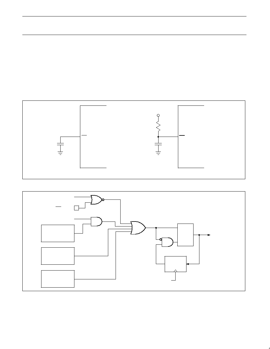
Philips Semiconductors
Product data
87LPC767
Low power, low price, low pin count (20 pin)
microcontroller with 4-kbyte OTP and 8-bit A/D converter
2001 Aug 07
30
Low Voltage EPROM Operation
The EPROM array contains some analog circuits that are not
required when V
DD
is less than 4 V, but are required for a V
DD
greater than 4 V. The LPEP bit (AUXR.4), when set by software, will
power down these analog circuits resulting in a reduced supply
current. LPEP is cleared only by power-on reset, so it may be set
ONLY for applications that always operate with V
DD
less than 4 V.
Reset
The 87LPC767 has an active low reset input when configured for an
external reset. A fully internal reset may also be configured which
provides a reset when power is initially applied to the device. The
watchdog timer can act as an oscillator fail detect because it uses
an independent, fully on-chip oscillator.
The external reset input is disabled, and fully internal reset
generation enabled, by programming the RPD bit in the EPROM
configuration register UCFG1 to 0. EPROM configuration is
described in the section EPROM Characteristics
SU01359
87LPC767
87LPC767
V
DD
8.2 k
W
10
m
F
RST
RST
2.2
m
F
Figure 22. Typical External Reset Circuits
SU01170
CHIP RESET
CPU
CLOCK
Q
RESET
TIMING
RPD (UCFG1.6)
WDT
MODULE
SOFTWARE RESET
SRST (AUXR1.3)
POWER MONITOR
RESET
RST/V
PP
PIN
WDTE (UCFG1.7)
S
R
Figure 23. Block Diagram Showing Reset Sources

Philips Semiconductors
Product data
87LPC767
Low power, low price, low pin count (20 pin)
microcontroller with 4-kbyte OTP and 8-bit A/D converter
2001 Aug 07
31
Timer/Counters
The 87LPC767 has two general purpose counter/timers which are
upward compatible with the standard 80C51 Timer 0 and Timer 1.
Both can be configured to operate either as timers or event counters
(see Figure 24). An option to automatically toggle the T0 and/or T1
pins upon timer overflow has been added.
In the "Timer" function, the register is incremented every machine
cycle. Thus, one can think of it as counting machine cycles. Since a
machine cycle consists of 6 CPU clock periods, the count rate is 1/6
of the CPU clock frequency. Refer to the section Enhanced CPU for
a description of the CPU clock.
In the "Counter" function, the register is incremented in response to
a 1-to-0 transition at its corresponding external input pin, T0 or T1.
In this function, the external input is sampled once during every
machine cycle. When the samples of the pin state show a high in
one cycle and a low in the next cycle, the count is incremented. The
new count value appears in the register during the cycle following
the one in which the transition was detected. Since it takes 2
machine cycles (12 CPU clocks) to recognize a 1-to-0 transition, the
maximum count rate is 1/6 of the CPU clock frequency. There are no
restrictions on the duty cycle of the external input signal, but to
ensure that a given level is sampled at least once before it changes,
it should be held for at least one full machine cycle.
The "Timer" or "Counter" function is selected by control bits C/T in
the Special Function Register TMOD. In addition to the "Timer" or
"Counter" selection, Timer 0 and Timer 1 have four operating
modes, which are selected by bit-pairs (M1, M0) in TMOD. Modes 0,
1, and 2 are the same for both Timers/Counters. Mode 3 is different.
The four operating modes are described in the following text.
BIT
SYMBOL
FUNCTION
TMOD.7
GATE
Gating control for Timer 1. When set, Timer/Counter is enabled only while the INT1 pin is high and
the TR1 control pin is set. When cleared, Timer 1 is enabled when the TR1 control bit is set.
TMOD.6
C/T
Timer or Counter Selector for Timer 1. Cleared for Timer operation (input from internal system clock.)
Set for Counter operation (input from T1 input pin).
TMOD.5, 4
M1, M0
Mode Select for Timer 1 (see table below).
TMOD.3
GATE
Gating control for Timer 0. When set, Timer/Counter is enabled only while the INT0 pin is high and
the TR0 control pin is set. When cleared, Timer 0 is enabled when the TR0 control bit is set.
TMOD.2
C/T
Timer or Counter Selector for Timer 0. Cleared for Timer operation (input from internal system clock.)
Set for Counter operation (input from T0 input pin).
TMOD.1, 0
M1, M0
Mode Select for Timer 0 (see table below).
M1, M0
Timer Mode
0 0
8048 Timer "TLn" serves as 5-bit prescaler.
0 1
16-bit Timer/Counter "THn" and "TLn" are cascaded; there is no prescaler.
1 0
8-bit auto-reload Timer/Counter. THn holds a value which is loaded into TLn when it overflows.
1 1
Timer 0 is a dual 8-bit Timer/Counter in this mode. TL0 is an 8-bit Timer/Counter controlled by the
standard Timer 0 control bits. TH0 is an 8-bit timer only, controlled by the Timer 1 control bits (see
text). Timer 1 in this mode is stopped.
M0
SU01171
M1
C/T
GATE
M0
M1
C/T
GATE
0
1
2
3
4
5
6
7
TMOD
Reset Value: 00h
Not Bit Addressable
Address: 89h
Figure 24. Timer/Counter Mode Control Register (TMOD)

Philips Semiconductors
Product data
87LPC767
Low power, low price, low pin count (20 pin)
microcontroller with 4-kbyte OTP and 8-bit A/D converter
2001 Aug 07
32
Mode 0
Putting either Timer into Mode 0 makes it look like an 8048 Timer,
which is an 8-bit Counter with a divide-by-32 prescaler. Figure 26
shows Mode 0 operation.
In this mode, the Timer register is configured as a 13-bit register. As
the count rolls over from all 1s to all 0s, it sets the Timer interrupt
flag TFn. The count input is enabled to the Timer when TRn = 1 and
either GATE = 0 or INTn = 1. (Setting GATE = 1 allows the Timer to
be controlled by external input INTn, to facilitate pulse width
measurements). TRn is a control bit in the Special Function Register
TCON (Figure 25). The GATE bit is in the TMOD register.
The 13-bit register consists of all 8 bits of THn and the lower 5 bits
of TLn. The upper 3 bits of TLn are indeterminate and should be
ignored. Setting the run flag (TRn) does not clear the registers.
Mode 0 operation is the same for Timer 0 and Timer 1. See
Figure 26. There are two different GATE bits, one for Timer 1
(TMOD.7) and one for Timer 0 (TMOD.3).
BIT
SYMBOL
FUNCTION
TCON.7
TF1
Timer 1 overflow flag. Set by hardware on Timer/Counter overflow. Cleared by hardware when the
interrupt is processed, or by software.
TCON.6
TR1
Timer 1 Run control bit. Set/cleared by software to turn Timer/Counter 1 on/off.
TCON.5
TF0
Timer 0 overflow flag. Set by hardware on Timer/Counter overflow. Cleared by hardware when the
processor vectors to the interrupt routine, or by software.
TCON.4
TR0
Timer 0 Run control bit. Set/cleared by software to turn Timer/Counter 0 on/off.
TCON.3
IE1
Interrupt 1 Edge flag. Set by hardware when external interrupt 1 edge is detected. Cleared by
hardware when the interrupt is processed, or by software.
TCON.2
IT1
Interrupt 1 Type control bit. Set/cleared by software to specify falling edge/low level triggered
external interrupts.
TCON.1
IE0
Interrupt 0 Edge flag. Set by hardware when external interrupt 0 edge is detected. Cleared by
hardware when the interrupt is processed, or by software.
TCON.0
IT0
Interrupt 0 Type control bit. Set/cleared by software to specify falling edge/low level triggered
external interrupts.
IT0
SU01172
IE0
IT1
IE1
TR0
TF0
TR1
TF1
0
1
2
3
4
5
6
7
TCON
Reset Value: 00h
Bit Addressable
Address: 88h
Figure 25. Timer/Counter Control Register (TCON)
SU01173
TLN
(5-BITS)
THN
(8-BITS)
OSC/6 OR
OSC/12
OVERFLOW
Tn PIN
TnOE
TOGGLE
CONTROL
C/T = 1
C/T = 0
Tn PIN
TRn
GATE
INTn PIN
INTERRUPT
TFn
Figure 26. Timer/Counter 0 or 1 in Mode 0 (13-Bit Counter)
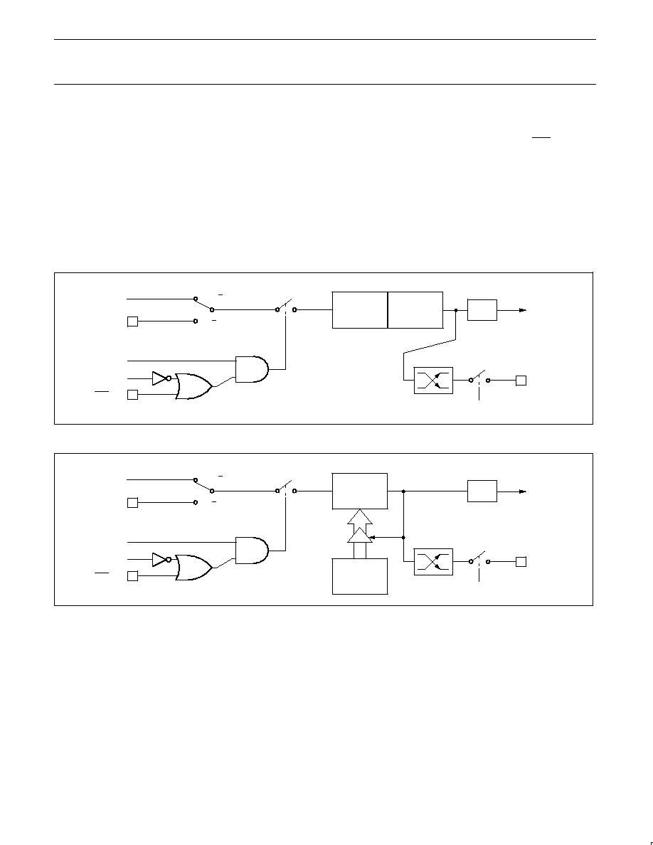
Philips Semiconductors
Product data
87LPC767
Low power, low price, low pin count (20 pin)
microcontroller with 4-kbyte OTP and 8-bit A/D converter
2001 Aug 07
33
Mode 1
Mode 1 is the same as Mode 0, except that all 16 bits of the timer
register (THn and TLn) are used. See Figure 27
Mode 2
Mode 2 configures the Timer register as an 8-bit Counter (TL1) with
automatic reload, as shown in Figure 28. Overflow from TLn not only
sets TFn, but also reloads TLn with the contents of THn, which must
be preset by software. The reload leaves THn unchanged. Mode 2
operation is the same for Timer 0 and Timer 1.
Mode 3
When Timer 1 is in Mode 3 it is stopped. The effect is the same as
setting TR1 = 0.
Timer 0 in Mode 3 establishes TL0 and TH0 as two separate 8-bit
counters. The logic for Mode 3 on Timer 0 is shown in Figure 29.
TL0 uses the Timer 0 control bits: C/T, GATE, TR0, INT0, and TF0.
TH0 is locked into a timer function (counting machine cycles) and
takes over the use of TR1 and TF1 from Timer 1. Thus, TH0 now
controls the "Timer 1" interrupt.
Mode 3 is provided for applications that require an extra 8-bit timer.
With Timer 0 in Mode 3, an 87LPC767 can look like it has three
Timer/Counters. When Timer 0 is in Mode 3, Timer 1 can be turned
on and off by switching it into and out of its own Mode 3. It can still
be used by the serial port as a baud rate generator, or in any
application not requiring an interrupt.
SU01174
TLN
(8-BITS)
THN
(8-BITS)
OSC/6 OR
OSC/12
OVERFLOW
Tn PIN
TnOE
TOGGLE
CONTROL
C/T = 1
C/T = 0
Tn PIN
TRn
GATE
INTn PIN
INTERRUPT
TFn
Figure 27. Timer/Counter 0 or 1 in Mode 1 (16-Bit Counter)
SU01392
TLN
(8-BITS)
THN
(8-BITS)
OSC/6 OR
OSC/12
OVERFLOW
Tn PIN
TnOE
TOGGLE
CONTROL
C/T = 1
C/T = 0
Tn PIN
TRn
GATE
INTn PIN
INTERRUPT
TFn
RELOAD
Figure 28. Timer/Counter 0 or 1 in Mode 2 (8-Bit Auto-Reload)
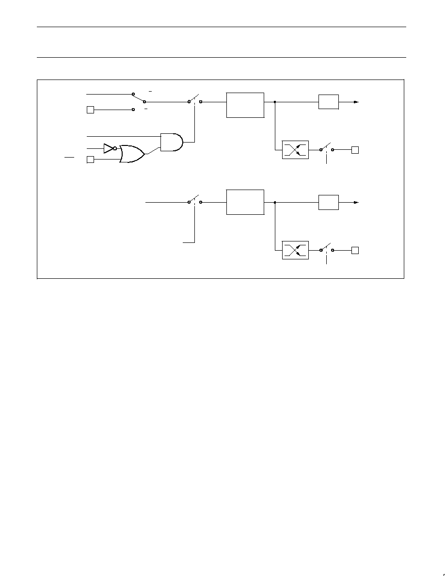
Philips Semiconductors
Product data
87LPC767
Low power, low price, low pin count (20 pin)
microcontroller with 4-kbyte OTP and 8-bit A/D converter
2001 Aug 07
34
SU01176
TL0
(8-BITS)
OSC/6 OR
OSC/12
OVERFLOW
T0 PIN
T0OE
TOGGLE
CONTROL
C/T = 1
C/T = 0
T0 PIN
TR0
GATE
INT0 PIN
INTERRUPT
TF0
TH0
(8-BITS)
OVERFLOW
T1 PIN
T1OE
TOGGLE
CONTROL
INTERRUPT
TF1
TR1
OSC/6 OR
OSC/12
Figure 29. Timer/Counter 0 Mode 3 (Two 8-Bit Counters)
Timer Overflow Toggle Output
Timers 0 and 1 can be configured to automatically toggle a port
output whenever a timer overflow occurs. The same device pins that
are used for the T0 and T1 count inputs are also used for the timer
toggle outputs. This function is enabled by control bits T0OE and
T1OE in the P2M1 register, and apply to Timer 0 and Timer 1
respectively. The port outputs will be a logic 1 prior to the first timer
overflow when this mode is turned on.
UART
The 87LPC767 includes an enhanced 80C51 UART. The baud rate
source for the UART is timer 1 for modes 1 and 3, while the rate is
fixed in modes 0 and 2. Because CPU clocking is different on the
87LPC767 than on the standard 80C51, baud rate calculation is
somewhat different. Enhancements over the standard 80C51 UART
include Framing Error detection and automatic address recognition.
The serial port is full duplex, meaning it can transmit and receive
simultaneously. It is also receive-buffered, meaning it can
commence reception of a second byte before a previously received
byte has been read from the SBUF register. However, if the first byte
still hasn't been read by the time reception of the second byte is
complete, the first byte will be lost. The serial port receive and
transmit registers are both accessed through Special Function
Register SBUF. Writing to SBUF loads the transmit register, and
reading SBUF accesses a physically separate receive register.
The serial port can be operated in 4 modes:
Mode 0
Serial data enters and exits through RxD. TxD outputs the shift
clock. 8 bits are transmitted or received, LSB first. The baud rate is
fixed at 1/6 of the CPU clock frequency.
Mode 1
10 bits are transmitted (through TxD) or received (through RxD): a
start bit (logical 0), 8 data bits (LSB first), and a stop bit (logical 1).
When data is received, the stop bit is stored in RB8 in Special
Function Register SCON. The baud rate is variable and is
determined by the Timer 1 overflow rate.
Mode 2
11 bits are transmitted (through TxD) or received (through RxD):
start bit (logical 0), 8 data bits (LSB first), a programmable 9th data
bit, and a stop bit (logical 1). When data is transmitted, the 9th data
bit (TB8 in SCON) can be assigned the value of 0 or 1. Or, for
example, the parity bit (P, in the PSW) could be moved into TB8.
When data is received, the 9th data bit goes into RB8 in Special
Function Register SCON, while the stop bit is ignored. The baud
rate is programmable to either 1/16 or 1/32 of the CPU clock
frequency, as determined by the SMOD1 bit in PCON.
Mode 3
11 bits are transmitted (through TxD) or received (through RxD): a
start bit (logical 0), 8 data bits (LSB first), a programmable 9th data
bit, and a stop bit (logical 1). In fact, Mode 3 is the same as Mode 2
in all respects except baud rate. The baud rate in Mode 3 is variable
and is determined by the Timer 1 overflow rate.
In all four modes, transmission is initiated by any instruction that
uses SBUF as a destination register. Reception is initiated in Mode 0
by the condition RI = 0 and REN = 1. Reception is initiated in the
other modes by the incoming start bit if REN = 1.

Philips Semiconductors
Product data
87LPC767
Low power, low price, low pin count (20 pin)
microcontroller with 4-kbyte OTP and 8-bit A/D converter
2001 Aug 07
35
Serial Port Control Register (SCON)
The serial port control and status register is the Special Function
Register SCON, shown in Figure 30. This register contains not only
the mode selection bits, but also the 9th data bit for transmit and
receive (TB8 and RB8), and the serial port interrupt bits (TI and RI).
The Framing Error bit (FE) allows detection of missing stop bits in
the received data stream. The FE bit shares the bit position SCON.7
with the SM0 bit. Which bit appears in SCON at any particular time
is determined by the SMOD0 bit in the PCON register. If SMOD0 =
0, SCON.7 is the SM0 bit. If SMOD0 = 1, SCON.7 is the FE bit.
Once set, the FE bit remains set until it is cleared by software. This
allows detection of framing errors for a group of characters without
the need for monitoring it for every character individually.
BIT
SYMBOL
FUNCTION
SCON.7
FE
Framing Error. This bit is set by the UART receiver when an invalid stop bit is detected. Must be
cleared by software. The SMOD0 bit in the PCON register must be 1 for this bit to be accessible.
See SM0 bit below.
SCON.7
SM0
With SM1, defines the serial port mode. The SMOD0 bit in the PCON register must be 0 for this bit
to be accessible. See FE bit above.
SCON. 6
SM1
With SM0, defines the serial port mode (see table below).
SM0, SM1
UART Mode
Baud Rate
0 0
0: shift register
CPU clock/6
0 1
1: 8-bit UART
Variable (see text)
1 0
2: 9-bit UART
CPU clock/32 or CPU clock/16
1 1
3: 9-bit UART
Variable (see text)
SCON.5
SM2
Enables the multiprocessor communication feature in Modes 2 and 3. In Mode 2 or 3, if SM2 is set
to 1, then Rl will not be activated if the received 9th data bit (RB8) is 0. In Mode 1, if SM2=1 then RI
will not be activated if a valid stop bit was not received. In Mode 0, SM2 should be 0.
SCON.4
REN
Enables serial reception. Set by software to enable reception. Clear by software to disable reception.
SCON.3
TB8
The 9th data bit that will be transmitted in Modes 2 and 3. Set or clear by software as desired.
SCON.2
RB8
In Modes 2 and 3, is the 9th data bit that was received. In Mode 1, it SM2=0, RB8 is the stop bit that
was received. In Mode 0, RB8 is not used.
SCON.1
TI
Transmit interrupt flag. Set by hardware at the end of the 8th bit time in Mode 0, or at the beginning
of the stop bit in the other modes, in any serial transmission. Must be cleared by software.
SCON.0
RI
Receive interrupt flag. Set by hardware at the end of the 8th bit time in Mode 0, or halfway through
the stop bit time in the other modes, in any serial reception (except see SM2). Must be cleared by
software.
RI
SU01157
TI
RB8
TB8
REN
SM2
SM1
SM0/FE
0
1
2
3
4
5
6
7
SCON
Reset Value: 00h
Bit Addressable
Address: 98h
Figure 30. Serial Port Control Register (SCON)
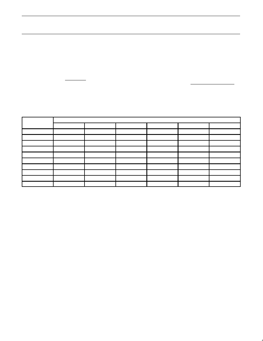
Philips Semiconductors
Product data
87LPC767
Low power, low price, low pin count (20 pin)
microcontroller with 4-kbyte OTP and 8-bit A/D converter
2001 Aug 07
36
Baud Rates
The baud rate in Mode 0 is fixed: Mode 0 Baud Rate = CPU clock/6.
The baud rate in Mode 2 depends on the value of bit SMOD1 in
Special Function Register PCON. If SMOD1 = 0 (which is the value
on reset), the baud rate is 1/32 of the CPU clock frequency. If
SMOD1 = 1, the baud rate is 1/16 of the CPU clock frequency.
Mode 2 Baud Rate
+
1
)
SMOD1
32
CPU clock frequency
Using Timer 1 to Generate Baud Rates
When Timer 1 is used as the baud rate generator, the baud rates in
Modes 1 and 3 are determined by the Timer 1 overflow rate and the
value of SMOD1. The Timer 1 interrupt should be disabled in this
application. The Timer itself can be configured for either "timer" or
"counter" operation, and in any of its 3 running modes. In the most
typical applications, it is configured for "timer" operation, in the
auto-reload mode (high nibble of TMOD = 0010b). In that case the
baud rate is given by the formula:
Mode 1, 3 Baud Rate
+
CPU clock frequency
192 (or 96 if SMOD1
+
1)
256
*
(TH1)
Tables 6 and 7 list various commonly used baud rates and how they
can be obtained using Timer 1 as the baud rate generator.
Table 9. Baud Rates, Timer Values, and CPU Clock Frequencies for SMOD1 = 0
Timer Co nt
Baud Rate
Timer Count
2400
4800
9600
19.2k
38.4k
57.6k
≠1
0.4608
0.9216
* 1.8432
* 3.6864
* 7.3728
* 11.0592
≠2
0.9216
1.8432
* 3.6864
* 7.3728
* 14.7456
≠3
1.3824
2.7648
5.5296
* 11.0592
≠
≠
≠4
* 1.8432
* 3.6864
* 7.3728
* 14.7456
≠
≠
≠5
2.3040
4.6080
9.2160
* 18.4320
≠
≠
≠6
2.7648
5.5296
* 11.0592
≠
≠
≠
≠7
3.2256
6.4512
12.9024
≠
≠
≠
≠8
* 3.6864
* 7.3728
* 14.7456
≠
≠
≠
≠9
4.1472
8.2944
16.5888
≠
≠
≠
≠10
4.6080
9.2160
* 18.4320
≠
≠
≠

Philips Semiconductors
Product data
87LPC767
Low power, low price, low pin count (20 pin)
microcontroller with 4-kbyte OTP and 8-bit A/D converter
2001 Aug 07
37
Table 10. Baud Rates, Timer Values, and CPU Clock Frequencies for SMOD1 = 1
Timer Co nt
Baud Rate
Timer Count
2400
4800
9600
19.2k
38.4k
57.6k
115.2k
≠1
0.2304
0.4608
0.9216
* 1.8432
* 3.6864
5.5296
* 11.0592
≠2
0.4608
0.9216
* 1.8432
* 3.6864
* 7.3728
* 11.0592
≠
≠3
0.6912
1.3824
2.7648
5.5296
* 11.0592
16.5888
≠
≠4
0.9216
* 1.8432
* 3.6864
* 7.3728
* 14.7456
≠
≠
≠5
1.1520
2.3040
4.6080
9.2160
* 18.4320
≠
≠
≠6
1.3824
2.7648
5.5296
* 11.0592
≠
≠
≠
≠7
1.6128
3.2256
6.4512
12.9024
≠
≠
≠
≠8
* 1.8432
* 3.6864
* 7.3728
* 14.7456
≠
≠
≠
≠9
2.0736
4.1472
8.2944
16.5888
≠
≠
≠
≠10
2.3040
4.6080
9.2160
* 18.4320
≠
≠
≠
≠11
2.5344
5.0688
10.1376
≠
≠
≠
≠
≠12
2.7648
5.5296
* 11.0592
≠
≠
≠
≠
≠13
2.9952
5.9904
11.9808
≠
≠
≠
≠
≠14
3.2256
6.4512
12.9024
≠
≠
≠
≠
≠15
3.4560
6.9120
13.8240
≠
≠
≠
≠
≠16
* 3.6864
* 7.3728
* 14.7456
≠
≠
≠
≠
≠17
3.9168
7.8336
15.6672
≠
≠
≠
≠
≠18
4.1472
8.2944
16.5888
≠
≠
≠
≠
≠19
4.3776
8.7552
17.5104
≠
≠
≠
≠
≠20
4.6080
9.2160
* 18.4320
≠
≠
≠
≠
≠21
4.8384
9.6768
19.3536
≠
≠
≠
≠
NOTES TO TABLES 9 AND 10:
1. Tables 6 and 7 apply to UART modes 1 and 3 (variable rate modes), and show CPU clock rates in MHz for standard baud rates from 2400 to
115.2k baud.
2. Table 6 shows timer settings and CPU clock rates with the SMOD1 bit in the PCON register = 0 (the default after reset), while Table 7
reflects the SMOD1 bit = 1.
3. The tables show all potential CPU clock frequencies up to 20 MHz that may be used for baud rates from 9600 baud to 115.2k baud. Other
CPU clock frequencies that would give only lower baud rates are not shown.
4. Table entries marked with an asterisk (*) indicate standard crystal and ceramic resonator frequencies that may be obtained from many
sources without special ordering.

Philips Semiconductors
Product data
87LPC767
Low power, low price, low pin count (20 pin)
microcontroller with 4-kbyte OTP and 8-bit A/D converter
2001 Aug 07
38
More About UART Mode 0
Serial data enters and exits through RxD. TxD outputs the shift
clock. 8 bits are transmitted/received: 8 data bits (LSB first). The
baud rate is fixed at 1/6 the CPU clock frequency. Figure 31 shows
a simplified functional diagram of the serial port in Mode 0, and
associated timing.
Transmission is initiated by any instruction that uses SBUF as a
destination register. The "write to SBUF" signal at S6P2 also loads a
1 into the 9th position of the transmit shift register and tells the TX
Control block to commence a transmission. The internal timing is
such that one full machine cycle will elapse between "write to SBUF"
and activation of SEND.
SEND enables the output of the shift register to the alternate output
function line of P1.1 and also enable SHIFT CLOCK to the alternate
output function line of P1.0. SHIFT CLOCK is low during S3, S4, and
S5 of every machine cycle, and high during S6, S1, and S2. At
S6P2 of every machine cycle in which SEND is active, the contents
of the transmit shift are shifted to the right one position.
As data bits shift out to the right, zeros come in from the left. When
the MSB of the data byte is at the output position of the shift register,
then the 1 that was initially loaded into the 9th position, is just to the
left of the MSB, and all positions to the left of that contain zeros. This
condition flags the TX Control block to do one last shift and then
deactivate SEND and set T1. Both of these actions occur at S1P1 of
the 10th machine cycle after "write to SBUF." Reception is initiated by
the condition REN = 1 and R1 = 0. At S6P2 of the next machine
cycle, the RX Control unit writes the bits 11111110 t o the receive shift
register, and in the next clock phase activates RECEIVE.
RECEIVE enable SHIFT CLOCK to the alternate output function line
of P1.0. SHIFT CLOCK makes transitions at S3P1 and S6P1 of every
machine cycle. At S6P2 of every machine cycle in which RECEIVE is
active, the contents of the receive shift register are shifted to the left
one position. The value that comes in from the right is the value that
was sampled at the P1.1 pin at S5P2 of the same machine cycle.
As data bits come in from the right, 1s shift out to the left. When the 0
that was initially loaded into the rightmost position arrives at the
leftmost position in the shift register, it flags the RX Control block to do
one last shift and load SBUF. At S1P1 of the 10th machine cycle after
the write to SCON that cleared RI, RECEIVE is cleared as RI is set.
More About UART Mode 1
Ten bits are transmitted (through TxD), or received (through RxD): a
start bit (0), 8 data bits (LSB first), and a stop bit (1). On receive, the
stop bit goes into RB8 in SCON. In the 87LPC767 the baud rate is
determined by the Timer 1 overflow rate. Figure 32 shows a
simplified functional diagram of the serial port in Mode 1, and
associated timings for transmit receive.
Transmission is initiated by any instruction that uses SBUF as a
destination register. The "write to SBUF" signal also loads a 1 into
the 9th bit position of the transmit shift register and flags the TX
Control unit that a transmission is requested. Transmission actually
commences at S1P1 of the machine cycle following the next rollover
in the divide-by-16 counter. (Thus, the bit times are synchronized to
the divide-by-16 counter, not to the "write to SBUF" signal.)
The transmission begins with activation of SEND which puts the
start bit at TxD. One bit time later, DATA is activated, which enables
the output bit of the transmit shift register to TxD. The first shift pulse
occurs one bit time after that.
As data bits shift out to the right, zeros are clocked in from the left.
When the MSB of the data byte is at the output position of the shift
register, then the 1 that was initially loaded into the 9th position is
just to the left of the MSB, and all positions to the left of that contain
zeros. This condition flags the TX Control unit to do one last shift
and then deactivate SEND and set TI. This occurs at the 10th
divide-by-16 rollover after "write to SBUF."
Reception is initiated by a detected 1-to-0 transition at RxD. For this
purpose RxD is sampled at a rate of 16 times whatever baud rate
has been established. When a transition is detected, the
divide-by-16 counter is immediately reset, and 1FFH is written into
the input shift register. Resetting the divide-by-16 counter aligns its
rollovers with the boundaries of the incoming bit times.
The 16 states of the counter divide each bit time into 16ths. At the
7th, 8th, and 9th counter states of each bit time, the bit detector
samples the value of RxD. The value accepted is the value that was
seen in at least 2 of the 3 samples. This is done for noise rejection.
If the value accepted during the first bit time is not 0, the receive
circuits are reset and the unit goes back to looking for another 1-to-0
transition. This is to provide rejection of false start bits. If the start bit
proves valid, it is shifted into the input shift register, and reception of
the rest of the frame will proceed.
As data bits come in from the right, 1s shift out to the left. When the
start bit arrives at the leftmost position in the shift register (which in
mode 1 is a 9-bit register), it flags the RX Control block to do one
last shift, load SBUF and RB8, and set RI. The signal to load SBUF
and RB8, and to set RI, will be generated if, and only if, the following
conditions are met at the time the final shift pulse is generated.: 1.
R1 = 0, and 2. Either SM2 = 0, or the received stop bit = 1.
If either of these two conditions is not met, the received frame is
irretrievably lost. If both conditions are met, the stop bit goes into
RB8, the 8 data bits go into SBUF, and RI is activated. At this time,
whether the above conditions are met or not, the unit goes back to
looking for a 1-to-0 transition in RxD.
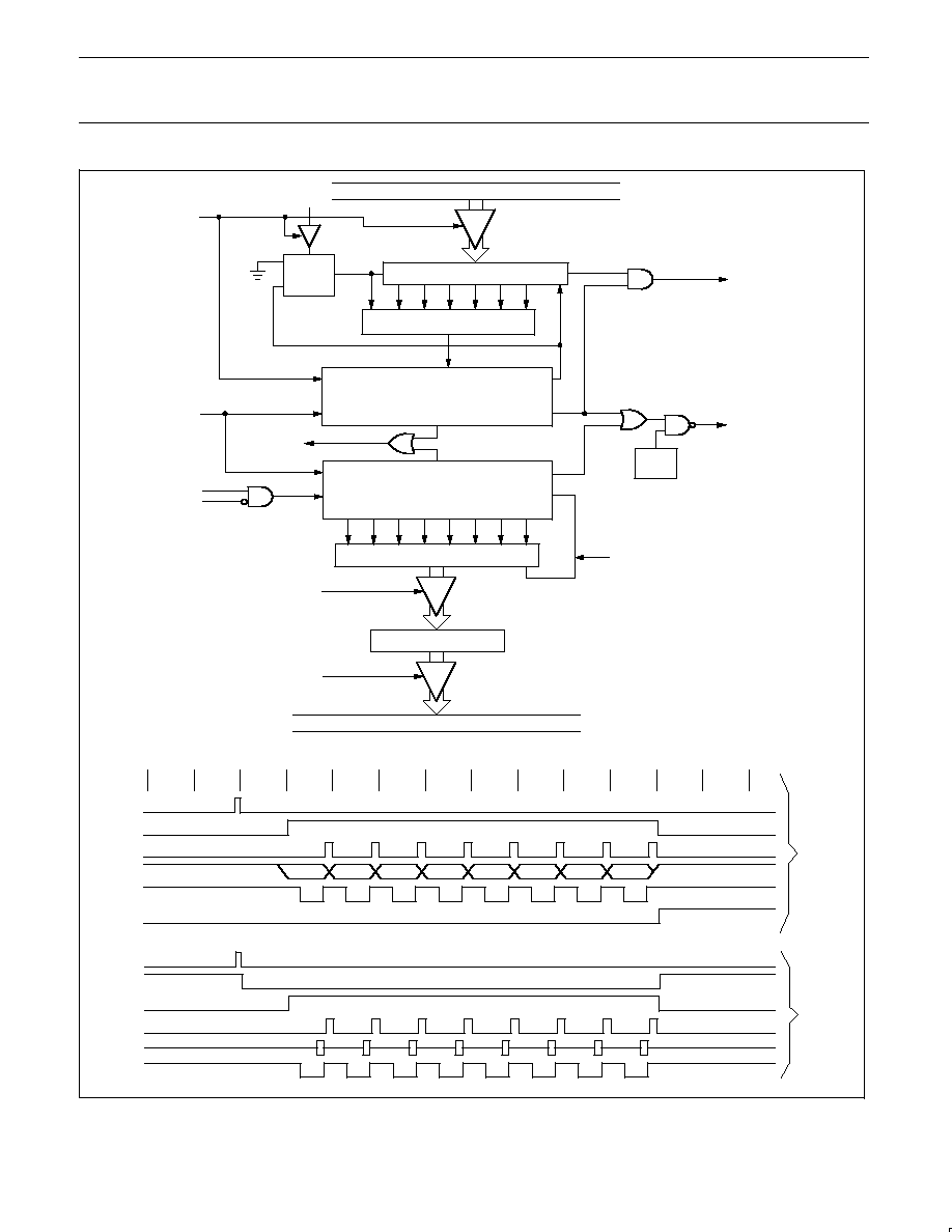
Philips Semiconductors
Product data
87LPC767
Low power, low price, low pin count (20 pin)
microcontroller with 4-kbyte OTP and 8-bit A/D converter
2001 Aug 07
39
80C51 INTERNAL BUS
SU01178
80C51 INTERNAL BUS
WRITE
TO
SBUF
SBUF
ZERO DETECTOR
RxD
P1.1 ALT
OUTPUT
FUNCTION
TX CONTROL
S
TX CLOCK
START
Q
CL
D
SERIAL PORT
INTERRUPT
SHIFT
CLOCK
SHIFT
SEND
S6
RXD
P1.1 ALT
INPUT
FUNCTION
LOAD
SBUF
TI
INPUT SHIFT REGISTER
START
RI
RECEIVE
SHIFT
TX CLOCK
RX CONTROL
REN
RI
SBUF
READ
SBUF
TRANSMIT
TxD
P1.0 ALT
OUTPUT
FUNCTION
SEND
RXD (DATA OUT)
D0
D1
D5
D2
D6
D3
D4
D7
TXD (SHIFT CLOCK)
SHIFT
S1 ... S6
S1 ... S6
S1 ... S6
S1 ... S6
S1 ... S6
S1 ... S6
S1 ... S6
S1 ... S6
S1 ... S6
S1 ... S6
S1 ... S6
S1 ... S6
S1 ... S6
WRITE TO SBUF
TI
RECEIVE
RECEIVE
D0
D1
D5
D2
D6
D3
D4
D7
TxD (SHIFT CLOCK)
SHIFT
WRITE TO SCON (CLEAR RI)
RI
RxD (DATA IN)
1
1
1
1
1
1
1
0
Figure 31. Serial Port Mode 0
Philips Semiconductors
Product data
87LPC767
Low power, low price, low pin count (20 pin)
microcontroller with 4-kbyte OTP and 8-bit A/D converter
2001 Aug 07
40
SU01179
80C51 INTERNAL BUS
WRITE
TO SBUF
SBUF
ZERO DETECTOR
TxD
P1.0 ALT
OUTPUT
FUNCTION
TX CONTROL
S
TX CLOCK
START
Q
CL
D
SERIAL PORT
INTERRUPT
SHIFT
SEND
LOAD
SBUF
TI
INPUT SHIFT REGISTER
START
RI
LOAD SBUF
SHIFT
RX
CLOCK
1FFH
RX CONTROL
SBUF
READ
SBUF
TRANSMIT
RxD
P1.1 ALT
INPUT
FUNCTION
80C51 INTERNAL BUS
DATA
TB8
˜
16
˜
16
˜
2
TIMER 1
OVERFLOW
SMOD1 = 0
SMOD1
= 1
1-TO-0
TRANSITION
DETECTOR
BIT
DETECTOR
START
BIT
STOP BIT
TX CLOCK
WRITE TO SBUF
SEND
DATA
SHIFT
TxD
TI
D0
D1
D5
D2
D6
D3
D4
D7
RECEIVE
RX CLOCK
SHIFT
RI
BIT DETECTOR SAMPLE TIMES
START
BIT
STOP BIT
RxD
D0
D1
D5
D2
D6
D3
D4
D7
˜
16 RESET
Figure 32. Serial Port Mode 1

Philips Semiconductors
Product data
87LPC767
Low power, low price, low pin count (20 pin)
microcontroller with 4-kbyte OTP and 8-bit A/D converter
2001 Aug 07
41
More About UART Modes 2 and 3
Eleven bits are transmitted (through TxD), or received (through
RxD): a start bit (0), 8 data bits (LSB first), a programmable 9th data
bit, and a stop bit (1). On transmit, the 9th data bit (TB8) can be
assigned the value of 0 or 1. On receive, the 9the data bit goes into
RB8 in SCON. The baud rate is programmable to either 1/16 or 1/32
of the CPU clock frequency in Mode 2. Mode 3 may have a variable
baud rate generated from Timer 1.
Figures 33 and 34 show a functional diagram of the serial port in
Modes 2 and 3. The receive portion is exactly the same as in Mode 1.
The transmit portion differs from Mode 1 only in the 9th bit of the
transmit shift register.
Transmission is initiated by any instruction that uses SBUF as a
destination register. The "write to SBUF" signal also loads TB8 into
the 9th bit position of the transmit shift register and flags the TX
Control unit that a transmission is requested. Transmission
commences at S1P1 of the machine cycle following the next rollover
in the divide-by-16 counter. (Thus, the bit times are synchronized to
the divide-by-16 counter, not to the "write to SBUF" signal.)
The transmission begins with activation of SEND, which puts the
start bit at TxD. One bit time later, DATA is activated, which enables
the output bit of the transmit shift register to TxD. The first shift pulse
occurs one bit time after that. The first shift clocks a 1 (the stop bit)
into the 9th bit position of the shift register. Thereafter, only zeros
are clocked in. Thus, as data bits shift out to the right, zeros are
clocked in from the left. When TB8 is at the output position of the
shift register, then the stop bit is just to the left of TB8, and all
positions to the left of that contain zeros. This condition flags the TX
Control unit to do one last shift and then deactivate SEND and set
TI. This occurs at the 11th divide-by-16 rollover after "write to SBUF."
Reception is initiated by a detected 1-to-0 transition at RxD. For this
purpose RxD is sampled at a rate of 16 times whatever baud rate
has been established. When a transition is detected, the
divide-by-16 counter is immediately reset, and 1FFH is written to the
input shift register.
At the 7th, 8th, and 9th counter states of each bit time, the bit
detector samples the value of R≠D. The value accepted is the value
that was seen in at least 2 of the 3 samples. If the value accepted
during the first bit time is not 0, the receive circuits are reset and the
unit goes back to looking for another 1-to-0 transition. If the start bit
proves valid, it is shifted into the input shift register, and reception of
the rest of the frame will proceed.
As data bits come in from the right, 1s shift out to the left. When the
start bit arrives at the leftmost position in the shift register (which in
Modes 2 and 3 is a 9-bit register), it flags the RX Control block to do
one last shift, load SBUF and RB8, and set RI.
The signal to load SBUF and RB8, and to set RI, will be generated
if, and only if, the following conditions are met at the time the final
shift pulse is generated. 1. RI = 0, and 2. Either SM2 = 0, or the
received 9th data bit = 1.
If either of these conditions is not met, the received frame is
irretrievably lost, and RI is not set. If both conditions are met, the
received 9th data bit goes into RB8, and the first 8 data bits go into
SBUF. One bit time later, whether the above conditions were met
or not, the unit goes back to looking for a 1-to-0 transition at the
RxD input.
Multiprocessor Communications
UART modes 2 and 3 have a special provision for multiprocessor
communications. In these modes, 9 data bits are received or
transmitted. When data is received, the 9th bit is stored in RB8. The
UART can be programmed such that when the stop bit is received,
the serial port interrupt will be activated only if RB8 = 1. This feature
is enabled by setting bit SM2 in SCON. One way to use this feature
in multiprocessor systems is as follows:
When the master processor wants to transmit a block of data to one
of several slaves, it first sends out an address byte which identifies
the target slave. An address byte differs from a data byte in that the
9th bit is 1 in an address byte and 0 in a data byte. With SM2 = 1, no
slave will be interrupted by a data byte. An address byte, however,
will interrupt all slaves, so that each slave can examine the received
byte and see if it is being addressed. The addressed slave will clear
its SM2 bit and prepare to receive the data bytes that follow. The
slaves that weren't being addressed leave their SM2 bits set and go
on about their business, ignoring the subsequent data bytes.
SM2 has no effect in Mode 0, and in Mode 1 can be used to check
the validity of the stop bit, although this is better done with the
Framing Error flag. In a Mode 1 reception, if SM2 = 1, the receive
interrupt will not be activated unless a valid stop bit is received.
Philips Semiconductors
Product data
87LPC767
Low power, low price, low pin count (20 pin)
microcontroller with 4-kbyte OTP and 8-bit A/D converter
2001 Aug 07
42
START
BIT
SU01180
80C51 INTERNAL BUS
WRITE TO SBUF
SBUF
ZERO DETECTOR
TxD
P1.0 ALT OUTPUT
FUNCTION
TX CONTROL
S
TX CLOCK
START
Q
CL
D
SERIAL PORT INTERRUPT
SHIFT
SEND
LOAD
SBUF
TI
INPUT SHIFT REGISTER
START
RI
LOAD SBUF
SHIFT
RX
CLOCK
1FFH
RX CONTROL
SBUF
READ
SBUF
RxD
P1.1 ALT
INPUT
FUNCTION
80C51 INTERNAL BUS
DATA
TB8
˜
16
˜
16
˜
2
PHASE 2 CLOCK
(1/2 f
OSC
)
1-TO-0
TRANSITION
DETECTOR
BIT DETECTOR
STOP BIT GEN.
SMOD1 = 0
SMOD1
= 1
TRANSMIT
START
BIT
STOP BIT
TX CLOCK
WRITE TO SBUF
SEND
DATA
SHIFT
TxD
TI
D0
D1
D5
D2
D6
D3
D4
D7
RECEIVE
RX CLOCK
SHIFT
RI
BIT DETECTOR SAMPLE TIMES
STOP BIT
RxD
D0
D1
D5
D2
D6
D3
D4
D7
˜
16 RESET
TB8
STOP BIT GEN.
RB8
Figure 33. Serial Port Mode 2
Philips Semiconductors
Product data
87LPC767
Low power, low price, low pin count (20 pin)
microcontroller with 4-kbyte OTP and 8-bit A/D converter
2001 Aug 07
43
BIT
DETECTOR
SU01181
TRANSMIT
START
BIT
STOP BIT
TX CLOCK
WRITE TO SBUF
SEND
DATA
SHIFT
TxD
TI
D0
D1
D5
D2
D6
D3
D4
D7
RECEIVE
RX CLOCK
SHIFT
RI
BIT DETECTOR SAMPLE TIMES
START
BIT
STOP BIT
RxD
D0
D1
D5
D2
D6
D3
D4
D7
˜
16 RESET
TB8
STOP BIT GEN.
RB8
80C51 INTERNAL BUS
WRITE TO SBUF
SBUF
ZERO DETECTOR
TxD
P1.0 ALT
OUTPUT
FUNCTION
TX CONTROL
S
TX CLOCK
START
Q
CL
D
SERIAL PORT INTERRUPT
SHIFT
SEND
LOAD
SBUF
TI
INPUT SHIFT REGISTER
START
RI
LOAD SBUF
SHIFT
RX
CLOCK
1FFH
RX CONTROL
SBUF
READ
SBUF
RxD
P1.1 ALT
INPUT
FUNCTION
80C51 INTERNAL BUS
DATA
TB8
˜
16
˜
16
˜
2
TIMER 1
OVERFLOW
SMOD1 = 0
SMOD1
= 1
1-TO-0
TRANSITION
DETECTOR
Figure 34. Serial Port Mode 3

Philips Semiconductors
Product data
87LPC767
Low power, low price, low pin count (20 pin)
microcontroller with 4-kbyte OTP and 8-bit A/D converter
2001 Aug 07
44
Automatic Address Recognition
Automatic Address Recognition is a feature which allows the UART
to recognize certain addresses in the serial bit stream by using
hardware to make the comparisons. This feature saves a great deal
of software overhead by eliminating the need for the software to
examine every serial address which passes by the serial port. This
feature is enabled by setting the SM2 bit in SCON. In the 9 bit UART
modes, mode 2 and mode 3, the Receive Interrupt flag (RI) will be
automatically set when the received byte contains either the "Given"
address or the "Broadcast" address. The 9 bit mode requires that
the 9th information bit is a 1 to indicate that the received information
is an address and not data.
Using the Automatic Address Recognition feature allows a master to
selectively communicate with one or more slaves by invoking the
Given slave address or addresses. All of the slaves may be
contacted by using the Broadcast address. Two special Function
Registers are used to define the slave's address, SADDR, and the
address mask, SADEN. SADEN is used to define which bits in the
SADDR are to be used and which bits are "don't care". The SADEN
mask can be logically ANDed with the SADDR to create the "Given"
address which the master will use for addressing each of the slaves.
Use of the Given address allows multiple slaves to be recognized
while excluding others. The following examples will help to show the
versatility of this scheme:
Slave 0 SADDR
= 1100 0000
SADEN
= 1111 1101
Given
= 1100 00X0
Slave 1
SADDR
= 1100 0000
SADEN
= 1111 1110
Given
= 1100 000X
In the above example SADDR is the same and the SADEN data is
used to differentiate between the two slaves. Slave 0 requires a 0 in
bit 0 and it ignores bit 1. Slave 1 requires a 0 in bit 1 and bit 0 is
ignored. A unique address for Slave 0 would be 1100 0010 since
slave 1 requires a 0 in bit 1. A unique address for slave 1 would be
1100 0001 since a 1 in bit 0 will exclude slave 0. Both slaves can be
selected at the same time by an address which has bit 0 = 0 (for
slave 0) and bit 1 = 0 (for slave 1). Thus, both could be addressed
with 1100 0000.
In a more complex system the following could be used to select
slaves 1 and 2 while excluding slave 0:
Slave 0
SADDR
= 1100 0000
SADEN
= 1111 1001
Given
= 1100 0XX0
Slave 1
SADDR
= 1110 0000
SADEN
= 1111 1010
Given
= 1110 0X0X
Slave 2
SADDR
= 1110 0000
SADEN
= 1111 1100
Given
= 1110 00XX
In the above example the differentiation among the 3 slaves is in the
lower 3 address bits. Slave 0 requires that bit 0 = 0 and it can be
uniquely addressed by 1110 0110. Slave 1 requires that bit 1 = 0 and
it can be uniquely addressed by 1110 and 0101. Slave 2 requires
that bit 2 = 0 and its unique address is 1110 0011. To select Slaves 0
and 1 and exclude Slave 2 use address 1110 0100, since it is
necessary to make bit 2 = 1 to exclude slave 2. The Broadcast
Address for each slave is created by taking the logical OR of SADDR
and SADEN. Zeros in this result are treated as don't-cares. In most
cases, interpreting the don't-cares as ones, the broadcast address
will be FF hexadecimal. Upon reset SADDR and SADEN are loaded
with 0s. This produces a given address of all "don't cares" as well as
a Broadcast address of all "don't cares". This effectively disables the
Automatic Addressing mode and allows the microcontroller to use
standard UART drivers which do not make use of this feature.
Watchdog Timer
When enabled via the WDTE configuration bit, the watchdog timer is
operated from an independent, fully on-chip oscillator in order to
provide the greatest possible dependability. When the watchdog
feature is enabled, the timer must be fed regularly by software in
order to prevent it from resetting the CPU, and it cannot be turned off.
When disabled as a watchdog timer (via the WDTE bit in the UCFG1
configuration register), it may be used as an interval timer and may
generate an interrupt. The watchdog timer is shown in Figure 35.
The watchdog timeout time is selectable from one of eight values,
nominal times range from 16 milliseconds to 2.1 seconds. The
frequency tolerance of the independent watchdog RC oscillator is
±
37%. The timeout selections and other control bits are shown in
Figure 36. When the watchdog function is enabled, the WDCON
register may be written once during chip initialization in order to set
the watchdog timeout time. The recommended method of initializing
the WDCON register is to first feed the watchdog, then write to
WDCON to configure the WDS2≠0 bits. Using this method, the
watchdog initialization may be done any time within 10 milliseconds
after startup without a watchdog overflow occurring before the
initialization can be completed.
Since the watchdog timer oscillator is fully on-chip and independent
of any external oscillator circuit used by the CPU, it intrinsically
serves as an oscillator fail detection function. If the watchdog feature
is enabled and the CPU oscillator fails for any reason, the watchdog
timer will time out and reset the CPU.
When the watchdog function is enabled, the timer is deactivated
temporarily when a chip reset occurs from another source, such as
a power on reset, brownout reset, or external reset.
Watchdog Feed Sequence
If the watchdog timer is running, it must be fed before it times out in
order to prevent a chip reset from occurring. The watchdog feed
sequence consists of first writing the value 1Eh, then the value E1h
to the WDRST register. An example of a watchdog feed sequence is
shown below.
WDFeed:
mov
WDRST,#1eh
; First part of watchdog feed sequence.
mov
WDRST,#0e1h
; Second part of watchdog feed sequence.
The two writes to WDRST do not have to occur in consecutive
instructions. An incorrect watchdog feed sequence does not cause
any immediate response from the watchdog timer, which will still
time out at the originally scheduled time if a correct feed sequence
does not occur prior to that time.
After a chip reset, the user program has a limited time in which to
either feed the watchdog timer or change the timeout period. When
a low CPU clock frequency is used in the application, the number of
instructions that can be executed before the watchdog overflows
may be quite small.
Watchdog Reset
If a watchdog reset occurs, the internal reset is active for
approximately one microsecond. If the CPU clock was still running,
code execution will begin immediately after that. If the processor
was in Power Down mode, the watchdog reset will start the oscillator
and code execution will resume after the oscillator is stable.
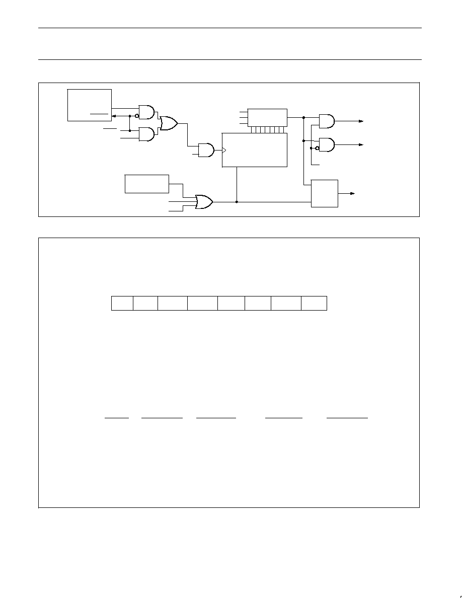
Philips Semiconductors
Product data
87LPC767
Low power, low price, low pin count (20 pin)
microcontroller with 4-kbyte OTP and 8-bit A/D converter
2001 Aug 07
45
SU01182
WATCHDOG
INTERRUPT
S
Q
20-BIT COUNTER
STATE CLOCK
WDTE (UCFG1.7)
BOD (xxx.x)
POR (xxx.x)
WATCHDOG
RESET
CLEAR
8 MSBs
8 TO 1 MUX
WATCHDOG
FEED DETECT
WDOVF
(WDCON.5)
WDS2≠0
(WDCON.2≠0)
WDTE + WDRUN
WDCLK * WDTE
500 kHz
R/C OSCILLATOR
ENABLE
CLOCK OUT
R
Figure 35. Block Diagram of the Watchdog Timer
BIT
SYMBOL
FUNCTION
WDCON.7, 6
--
Reserved for future use. Should not be set to 1 by user programs.
WDCON.5
WDOVF
Watchdog timer overflow flag. Set when a watchdog reset or timer overflow occurs. Cleared when
the watchdog is fed.
WDCON.4
WDRUN
Watchdog run control. The watchdog timer is started when WDRUN = 1 and stopped when
WDRUN = 0. This bit is forced to 1 (watchdog running) if the WDTE configuration bit = 1.
WDCON.3
WDCLK
Watchdog clock select. The watchdog timer is clocked by CPU clock/6 when WDCLK = 1 and by
the watchdog RC oscillator when WDCLK = 0. This bit is forced to 0 (using the watchdog RC
oscillator) if the WDTE configuration bit = 1.
WDCON.2≠0 WDS2≠0
Watchdog rate select.
WDS2≠0
Timeout Clocks
Minimum Time
Nominal Time
Maximum Time
0 0 0
8,192
10 ms
16 ms
23 ms
0 0 1
16,384
20 ms
32 ms
45 ms
0 1 0
32,768
41 ms
65 ms
90 ms
0 1 1
65,536
82 ms
131 ms
180 ms
1 0 0
131,072
165 ms
262 ms
360 ms
1 0 1
262,144
330 ms
524 ms
719 ms
1 1 0
524,288
660 ms
1.05 sec
1.44 sec
1 1 1
1,048,576
1.3 sec
2.1 sec
2.9 sec
WDS0
SU01183
WDS1
WDS2
WDCLK
WDRUN
WDOVF
--
--
0
1
2
3
4
5
6
7
WDCON
Reset Value:
S
30h for a watchdog reset.
S
10h for other rest sources if the watchdog is enabled via the WDTE configuration bit.
S
00h for other reset sources if the watchdog is disabled via the WDTE configuration bit.
Not Bit Addressable
Address: A7h
Figure 36. Watchdog Timer Control Register (WDCON)

Philips Semiconductors
Product data
87LPC767
Low power, low price, low pin count (20 pin)
microcontroller with 4-kbyte OTP and 8-bit A/D converter
2001 Aug 07
46
Additional Features
The AUXR1 register contains several special purpose control bits that
relate to several chip features. AUXR1 is described in Figure 37.
Software Reset
The SRST bit in AUXR1 allows software the opportunity to reset the
processor completely, as if an external reset or watchdog reset had
occurred. If a value is written to AUXR1 that contains a 1 at bit
position 3, all SFRs will be initialized and execution will resume at
program address 0000. Care should be taken when writing to
AUXR1 to avoid accidental software resets.
Dual Data Pointers
The dual Data Pointer (DPTR) adds to the ways in which the
processor can specify the address used with certain instructions.
The DPS bit in the AUXR1 register selects one of the two Data
Pointers. The DPTR that is not currently selected is not accessible
to software unless the DPS bit is toggled.
Specific instructions affected by the Data Pointer selection are:
∑
INC
DPTR
Increments the Data Pointer by 1.
∑
JMP
@A+DPTR
Jump indirect relative to DPTR value.
∑
MOV
DPTR, #data16
Load the Data Pointer with a 16-bit
constant.
∑
MOVC A, @A+DPTR
Move code byte relative to DPTR to the
accumulator.
∑
MOVX A, @DPTR
Move data byte the accumulator to data
memory relative to DPTR.
∑
MOVX @DPTR, A
Move data byte from data memory
relative to DPTR to the accumulator.
Also, any instruction that reads or manipulates the DPH and DPL
registers (the upper and lower bytes of the current DPTR) will be
affected by the setting of DPS. The MOVX instructions have limited
application for the 87LPC767 since the part does not have an
external data bus. However, they may be used to access EPROM
configuration information (see EPROM Characteristics section).
Bit 2 of AUXR1 is permanently wired as a logic 0. This is so that the
DPS bit may be toggled (thereby switching Data Pointers) simply by
incrementing the AUXR1 register, without the possibility of
inadvertently altering other bits in the register.
BIT
SYMBOL
FUNCTION
AUXR1.7
KBF
Keyboard Interrupt Flag. Set when any pin of port 0 that is enabled for the Keyboard Interrupt
function goes low. Must be cleared by software.
AUXR1.6
BOD
Brown Out Disable. When set, turns off brownout detection and saves power. See Power
Monitoring Functions section for details.
AUXR1.5
BOI
Brown Out Interrupt. When set, prevents brownout detection from causing a chip reset and allows
the brownout detect function to be used as an interrupt. See the Power Monitoring Functions
section for details.
AUXR1.4
LPEP
Low Power EPROM control bit. Allows power savings in low voltage systems. Set by software. Can
only be cleared by power-on or brownout reset. See the Power Reduction Modes section for
details.
AUXR1.3
SRST
Software Reset. When set by software, resets the 87LPC764 as if a hardware reset occurred.
AUXR1.2
--
This bit contains a hard-wired 0. Allows toggling of the DPS bit by incrementing AUXR1, without
interfering with other bits in the register.
AUXR1.1
--
Reserved for future use. Should not be set to 1 by user programs.
AUXR1.0
DPS
Data Pointer Select. Chooses one of two Data Pointers for use by the program. See text for details.
DPS
SU01184
--
0
SRST
LPEP
BOI
BOD
KBF
0
1
2
3
4
5
6
7
AUXR1
Reset Value: 00h
Not Bit Addressable
Address: A2h
Figure 37. AUXR1 Register

Philips Semiconductors
Product data
87LPC767
Low power, low price, low pin count (20 pin)
microcontroller with 4-kbyte OTP and 8-bit A/D converter
2001 Aug 07
47
EPROM Characteristics
Programming of the EPROM on the 87LPC767 is accomplished with
a serial programming method. Commands, addresses, and data are
transmitted to and from the device on two pins after programming
mode is entered. Serial programming allows easy implementation of
in-circuit programming of the 87LPC767 in an application board.
The 87LPC767 contains three signature bytes that can be read and
used by an EPROM programming system to identify the device. The
signature bytes designate the device as an 87LPC767 manufactured
by Philips. The signature bytes may be read by the user program at
addresses FC30h, FC31h and FC60h with the MOVC instruction,
using the DPTR register for addressing.
A special user data area is also available for access via the MOVC
instruction at addresses FCE0h through FCFFh. This "customer
code" space is programmed in the same manner as the main code
EPROM and may be used to store a serial number, manufacturing
date, or other application information.
32-Byte Customer Code Space
A small supplemental EPROM space is reserved for use by the
customer in order to identify code revisions, store checksums, add a
serial number to each device, or any other desired use. This area
exists in the code memory space from addresses FCE0h through
FCFFh. Code execution from this space is not supported, but it may
be read as data through the use of the MOVC instruction with the
appropriate addresses. The memory may be programmed at the
same time as the rest of the code memory and UCFG bytes are
programmed.
System Configuration Bytes
A number of user configurable features of the 87LPC767 must be
defined at power up and therefore cannot be set by the program after
start of execution. Those features are configured through the use of
two EPROM bytes that are programmed in the same manner as the
EPROM program space. The contents of the two configuration bytes,
UCFG1 and UCFG2, are shown in Figures 38 and 39. The values of
these bytes may be read by the program through the use of the
MOVX instruction at the addresses shown in the figure.
BIT
SYMBOL
FUNCTION
UCFG1.7
WDTE
Watchdog timer enable. When programmed (0), disables the watchdog timer. The timer may
still be used to generate an interrupt.
UCFG1.6
RPD
Reset pin disable. When 1 disables the reset function of pin P1.5, allowing it to be used as an
input only port pin.
UCFG1.5
PRHI
Port reset high. When 1, ports reset to a high state. When 0, ports reset to a low state.
UCFG1.4
BOV
Brownout voltage select. When 1, the brownout detect voltage is 2.5V. When 0, the brownout
detect voltage is 3.8V. This is described in the Power Monitoring Functions section.
UCFG1.3
CLKR
Clock rate select. When 0, the CPU clock rate is divided by 2. This results in machine cycles
taking 12 CPU clocks to complete as in the standard 80C51. For full backward compatibility,
this division applies to peripheral timing as well.
UCFG1.2≠0 FOSC2≠FSOC0
CPU oscillator type select. See Oscillator section for additional information. Combinations
other than those shown below should not be used. They are reserved for future use.
FOSC2≠FOSC0
Oscillator Configuration
1 1 1
External clock input on X1 (default setting for an unprogrammed part).
0 1 1
Internal RC oscillator, 6 MHz
±
25%.
0 1 0
Low frequency crystal, 20 kHz to 100 kHz.
0 0 1
Medium frequency crystal or resonator, 100 kHz to 4 MHz.
0 0 0
High frequency crystal or resonator, 4 MHz to 20 MHz.
FOSC0
SU01185
FOSC1
FOSC2
CLKR
BOV
PRHI
RPD
WDTE
0
1
2
3
4
5
6
7
UCFG1
Unprogrammed Value: FFh
Address: FD00h
Figure 38. EPROM System Configuration Byte 1 (UCFG1)

Philips Semiconductors
Product data
87LPC767
Low power, low price, low pin count (20 pin)
microcontroller with 4-kbyte OTP and 8-bit A/D converter
2001 Aug 07
48
BIT
SYMBOL
FUNCTION
UCFG2.7, 6
SB2, SB1
EPROM security bits. See table entitled, "EPROM Security Bits" for details.
UCFG2.5≠0
--
Reserved for future use.
--
SU01186
--
--
--
--
--
SB1
SB2
0
1
2
3
4
5
6
7
UCFG2
Unprogrammed Value: FFh
Address: FD01h
Figure 39. EPROM System Configuration Byte 2 (UCFG2)
Security Bits
When neither of the security bits are programmed, the code in the EPROM can be verified. When only security bit 1 is programmed, all further
programming of the EPROM is disabled. At that point, only security bit 2 may still be programmed. When both security bits are programmed,
EPROM verify is also disabled.
Table 11. EPROM Security Bits
SB2
SB1
Protection Description
1
1
Both security bits unprogrammed. No program security features enabled. EPROM is programmable and verifiable.
1
0
Only security bit 1 programmed. Further EPROM programming is disabled. Security bit 2 may still be programmed.
0
1
Only security bit 2 programmed. This combination is not supported.
0
0
Both security bits programmed. All EPROM verification and programming are disabled.
ABSOLUTE MAXIMUM RATINGS
PARAMETER
RATING
UNIT
Operating temperature under bias
≠55 to +125
∞
C
Storage temperature range
≠65 to +150
∞
C
Voltage on RST/V
PP
pin to V
SS
0 to +11.0
V
Voltage on any other pin to V
SS
≠0.5 to V
DD
+0.5 V
V
Maximum I
OL
per I/O pin
20
mA
Power dissipation (based on package heat transfer, not device power consumption)
1.5
W
NOTES:
1. Stresses above those listed under Absolute Maximum Ratings may cause permanent damage to the device. This is a stress rating only and
functional operation of the device at these or any conditions other than those described in the AC and DC Electrical Characteristics section
of this specification are not implied.
2. This product includes circuitry specifically designed for the protection of its internal devices from the damaging effects of excessive static
charge. Nonetheless, it is suggested that conventional precautions be taken to avoid applying greater than the rated maximum.
3. Parameters are valid over operating temperature range unless otherwise specified. All voltages are with respect to VSS unless otherwise noted.

Philips Semiconductors
Product data
87LPC767
Low power, low price, low pin count (20 pin)
microcontroller with 4-kbyte OTP and 8-bit A/D converter
2001 Aug 07
49
DC ELECTRICAL CHARACTERISTICS
V
DD
= 2.7 V to 6.0 V unless otherwise specified; T
amb
= 0
∞
C to +70
∞
C, ≠40
∞
C to +85
∞
C, or ≠40
∞
C to +125
∞
C, unless otherwise specified.
SYMBOL
PARAMETER
TEST CONDITIONS
LIMITS
UNIT
SYMBOL
PARAMETER
TEST CONDITIONS
MIN
TYP
1
MAX
UNIT
I
Power supply current operating
5.0 V, 20 MHz
11
15
25
mA
I
DD
Power supply current, operating
3.0 V, 10 MHz
11
4
7
mA
I
Power supply current Idle mode
5.0 V, 20 MHz
11
6
10
mA
I
ID
Power supply current, Idle mode
3.0 V, 10 MHz
11
2
4
mA
I
Power supply current Power Down mode
5.0 V
11
1
10
µ
A
I
PD
Power supply current, Power Down mode
3.0 V
11
1
5
µ
A
V
RAM
RAM keep-alive voltage
1.5
V
V
Input low voltage (TTL input)
4.0 V < V
DD
< 6.0 V
≠0.5
0.2 V
DD
≠0.1
V
V
IL
Input low voltage (TTL input)
2.7 V < V
DD
< 4.0 V
≠0.5
0.7
V
V
IL1
Negative going threshold (Schmitt input)
≠0.5 V
DD
0.4 V
DD
0.3 V
DD
V
V
IH
Input high voltage (TTL input)
0.2 V
DD
+0.9
V
DD
+0.5
V
V
IH1
Positive going threshold (Schmitt input)
0.7 V
DD
0.6 V
DD
V
DD
+0.5
V
HYS
Hysteresis voltage
0.2 V
DD
V
V
OL
Output low voltage all ports
5, 9
I
OL
= 3.2 mA, V
DD
= 2.7 V
0.4
V
V
OL1
Output low voltage all ports
5, 9
I
OL
= 20 mA, V
DD
= 2.7 V
1.0
V
V
O
Output high voltage all ports
3
I
OH
= ≠20
µ
A, V
DD
= 2.7 V
V
DD
≠0.7
V
V
OH
Output high voltage, all ports
3
I
OH
= ≠30
µ
A, V
DD
= 4.5 V
V
DD
≠0.7
V
V
OH1
Output high voltage, all ports
4
I
OH
= ≠1.0 mA, V
DD
= 2.7 V
V
DD
≠0.7
V
C
IO
Input/Output pin capacitance
10
15
pF
I
IL
Logical 0 input current, all ports
8
V
IN
= 0.4 V
≠50
µ
A
I
LI
Input leakage current, all ports
7
V
IN
= V
IL
or V
IH
±
2
µ
A
I
Logical 1 to 0 transition current all ports
3, 6
V
IN
= 1.5 V at V
DD
= 3.0 V
≠30
≠250
µ
A
I
TL
Logical 1 to 0 transition current, all ports
3, 6
V
IN
= 2.0 V at V
DD
= 5.5 V
≠150
≠650
µ
A
R
RST
Internal reset pull-up resistor
40
225
k
V
BO2.5
Brownout trip voltage with BOV = 1
12
T
amb
= 0
∞
C to +70
∞
C
2.45
2.5
2.65
V
V
BO3.8
Brownout trip voltage with BOV = 0
3.45
3.8
3.90
V
V
REF
Reference voltage
1.11
1.26
1.41
V
t
C
(V
REF
)
Temperature coefficient
tbd
ppm/
∞
C
SS
Supply sensitivity
tbd
%/V
NOTES:
1. Typical ratings are not guaranteed. The values listed are at room temperature, 5 V.
2. See other Figures for details.
Active mode: I
CC(MAX)
= tbd
Idle mode: I
CC(MAX)
= tbd
3. Ports in quasi-bidirectional mode with weak pull-up (applies to all port pins with pull-ups). Does not apply to open drain pins.
4. Ports in PUSH-PULL mode. Does not apply to open drain pins.
5. In all output modes except high impedance mode.
6. Port pins source a transition current when used in quasi-bidirectional mode and externally driven from 1 to 0. This current is highest when
V
IN
is approximately 2 V.
7. Measured with port in high impedance mode. Parameter is guaranteed but not tested at cold temperature.
8. Measured with port in quasi-bidirectional mode.
9. Under steady state (non-transient) conditions, I
OL
must be externally limited as follows:
Maximum I
OL
per port pin:
20 mA
Maximum total I
OL
for all outputs:
80 mA
Maximum total I
OH
for all outputs:
5 mA
If I
OL
exceeds the test condition, V
OL
may exceed the related specification. Pins are not guaranteed to sink current greater than the listed
test conditions.
10. Pin capacitance is characterized but not tested.
11. The I
DD
, I
ID
, and I
PD
specifications are measured using an external clock with the following functions disabled: comparators, brownout
detect, and watchdog timer. For V
DD
= 3 V, LPEP = 1. Refer to the appropriate figures on the following pages for additional current drawn by
each of these functions and detailed graphs for other frequency and voltage combinations.
12. Devices initially operating at V
DD
= 2.7 V or above and at f
OSC
= 10 MHz or less are guaranteed to continue to execute instructions correctly
at the brownout trip point. Initial power-on operation below V
DD
= 2.7 V is not guaranteed.
Philips Semiconductors
Product data
87LPC767
Low power, low price, low pin count (20 pin)
microcontroller with 4-kbyte OTP and 8-bit A/D converter
2001 Aug 07
50
COMPARATOR ELECTRICAL CHARACTERISTICS
V
DD
= 3.0 V to 6.0 V unless otherwise specified; T
amb
= 0
∞
C to +70
∞
C, ≠40
∞
C to +85
∞
C, or ≠40
∞
C to +125
∞
C, unless otherwise specified
SYMBOL
PARAMETER
TEST CONDITIONS
LIMITS
UNIT
SYMBOL
PARAMETER
TEST CONDITIONS
MIN
TYP
MAX
UNIT
V
IO
Offset voltage comparator inputs
1
±
10
mV
V
CR
Common mode range comparator inputs
0
V
DD
≠0.3
V
CMRR
Common mode rejection ratio
1
≠50
dB
Response time
250
500
ns
Comparator enable to output valid
10
µ
s
I
IL
Input leakage current, comparator
0 < V
IN
< V
DD
±
10
µ
A
NOTE:
1. This parameter is guaranteed by characterization, but not tested in production.
A/D CONVERTER DC ELECTRICAL CHARACTERISTICS
Vdd = 3.0 V to 6.0 V unless otherwise specified;
Tamb = 0 to +70
∞
C for commercial, -40
∞
C to +85
∞
C for industrial, or ≠40
∞
C to +125
∞
C for extended industrial, unless otherwise specified.
SYMBOL
PARAMETER
TEST CONDITIONS
LIMITS
UNIT
SYMBOL
PARAMETER
TEST CONDITIONS
MIN
MAX
UNIT
AV
IN
Analog input voltage
V
SS
- 0.2
V
DD
+ 0.2
V
R
REF
Resistance between V
DD
and V
SS
A/D enabled
tbd
tbd
k
C
IA
Analog input capacitance
15
pF
DL
e
Differential non-linearity
1,2,3
±
1
LSB
IL
e
Integral non-linearity
1,4
±
1
LSB
OS
e
Offset error
1,5
±
1
LSB
G
e
Gain error
1,6
±
1
%
A
e
Absolute voltage error
1,7
±
1
LSB
M
CTC
Channel-to-channel matching
±
1
LSB
C
t
Crosstalk between inputs of port
8
0 to 100 kHz
-60
dB
-
Input slew rate
100
V/ms
-
Input source impedance
10
k
NOTES:
1. Conditions: V
SS
= 0 V; V
DD
= 5.12 V.
2. The A/D is monotonic, there are no missing codes
3. The differential non-linearity (DL
e
) is the difference between the actual step width and the ideal step width. See Figure 40.
4. The integral non-linearity (IL
e
) is the peak difference between the center of the steps of the actual and the ideal transfer curve after
appropriate adjustment of gain and offset errors. See Figure 40.
5. The offset error (OS
e
) is the absolute difference between the straight line which fits the actual transfer curve (after removing gain error), and
the straight line which fits the ideal transfer curve. See Figure 40.
6. The gain error (G
e
) is the relative difference in percent between the straight line fitting the actual transfer curve (after removing offset error),
and the straight line which fits the ideal transfer curve. Gain error is constant at every point on the transfer curve. See Figure 40.
7. The absolute voltage error (A
e
) is the maximum difference between the center of the steps of the actual transfer curve of the non-calibrated
ADC and the ideal transfer curve.
8. This should be considered when both analog and digital signals are input simultaneously to A/D pins.
9. Changing the input voltage faster than this may cause erroneous readings.
10. A source impedance higher than this driving an A/D input may result in loss of precision and erroneous readings.
Philips Semiconductors
Product data
87LPC767
Low power, low price, low pin count (20 pin)
microcontroller with 4-kbyte OTP and 8-bit A/D converter
2001 Aug 07
51
255
254
253
252
251
(2)
(1)
256
250
251
252
253
254
255
7
1
2
3
4
5
6
7
6
5
4
3
2
1
0
250
(5)
(4)
(3)
1 LSB
(ideal)
Code
Out
Offset
error
OS
e
Gain
error
G
e
AV
IN
(LSB
ideal
)
Offset
error
OS
e
V
DD
- V
SS
1 LSB =
256
(1) Example of an actual transfer curve.
(2) The ideal transfer curve.
(3) Differential non-linearity (DL
e
).
(4) Integral non-linearity (IL
e
).
(5) Center of a step of the actual transfer curve.
SU01355
Figure 40. A/D Conversion Characteristics
Philips Semiconductors
Product data
87LPC767
Low power, low price, low pin count (20 pin)
microcontroller with 4-kbyte OTP and 8-bit A/D converter
2001 Aug 07
52
AC ELECTRICAL CHARACTERISTICS
T
amb
= 0
∞
C to +70
∞
C, ≠40
∞
C to +85
∞
C, or ≠40
∞
C to +125
∞
C; V
DD
= 2.7 V to 6.0 V unless otherwise specified, V
SS
= 0 V
1, 2, 3
SYMBOL
FIGURE
PARAMETER
LIMITS
UNIT
SYMBOL
FIGURE
PARAMETER
MIN
MAX
UNIT
External Clock
f
C
42
Oscillator frequency (V
DD
= 4.5 V to 6.0 V)
0
20
MHz
f
C
42
Oscillator frequency (V
DD
= 2.7 V to 6.0 V)
0
10
MHz
t
C
42
Clock period and CPU timing cycle
1/f
C
ns
t
CHCX
42
Clock high-time
4
20
ns
t
CLCX
42
Clock low time
4
20
ns
Shift Register
t
XLXL
41
Serial port clock cycle time
6t
C
ns
t
QVXH
41
Output data setup to clock rising edge
5t
C
≠ 133
ns
t
XHQX
41
Output data hold after clock rising edge
1t
C
≠ 80
ns
t
XHDV
41
Input data setup to clock rising edge
5t
C
≠ 133
ns
t
XHDX
41
Input data hold after clock rising edge
0
ns
NOTES:
1. Parameters are valid over operating temperature range unless otherwise specified.
2. Load capacitance for all outputs = 80 pF.
3. Parts are guaranteed to operate down to 0 Hz.
4. Applies only to an external clock source, not when a crystal is connected to the X1 and X2 pins.
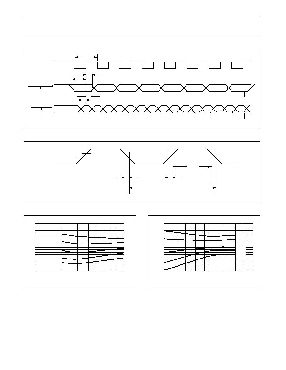
Philips Semiconductors
Product data
87LPC767
Low power, low price, low pin count (20 pin)
microcontroller with 4-kbyte OTP and 8-bit A/D converter
2001 Aug 07
53
CLEAR RI
t
XLXL
CLOCK
t
XHQX
t
QVXH
OUTPUT DATA
WRITE TO SBUF
INPUT DATA
t
XHDV
t
XHDX
SET TI
SET RI
SU01187
7
1
2
3
4
5
6
0
VALID
VALID
VALID
VALID
VALID
VALID
VALID
VALID
Figure 41. Shift Register Mode Timing
SU01188
V
DD
≠ 0.5
0.45V
0.2V
DD
+ 0.9
0.2 V
DD
≠ 0.1
t
CHCL
t
CLCH
t
CHCX
t
CLCX
t
C
Figure 42. External Clock Timing
SU01202
100
10
1
10
100
Idd (uA)
Frequency (kHz)
6.0 V
5.0 V
4.0 V
3.3 V
2.7 V
Figure 43. Typical Idd versus frequency (low frequency
oscillator, 25
∞
C)
SU01203
1000
100
10
100
10,000
Idd (uA)
Frequency (kHz)
1,000
6.0 V
5.0 V
2.7 V
6.0 V
5.0 V
4.0 V
3.3 V
2.7 V
Figure 44. Typical Idd versus frequency (medium frequency
oscillator, 25
∞
C)

Philips Semiconductors
Product data
87LPC767
Low power, low price, low pin count (20 pin)
microcontroller with 4-kbyte OTP and 8-bit A/D converter
2001 Aug 07
54
SU01204
10,000
1,000
100
1
100
Idd (uA)
Frequency (MHz)
10
6.0 V
5.0 V
4.0 V
3.3 V
2.7 V
Figure 45. Typical Idd versus frequency (high frequency
oscillator, 25
∞
C)
SU01205
100,000
100
10
10
100,000
Idd (uA)
Frequency (kHz)
1,000
10,000
6.0 V
5.0 V
4.0 V
3.3 V
2.7 V
100
1,000
10,000
Figure 46. Typical Active Idd versus frequency (external clock,
25
∞
C, LPEP = 0)
SU01206
10,000
100
1
10
10,000
Idd (uA)
Frequency (kHz)
4.0 V
3.3 V
2.7 V
100
1,000
1,000
10
Figure 47. Typical Active Idd versus frequency (external clock,
25
∞
C, LPEP = 1)
SU01207
100
10
1
10
100
Idd (uA)
Frequency (kHz)
4.0 V
3.3 V
2.7 V
1,000
10,000
1,000
10,000
Figure 48. Typical Idle Idd versus frequency (external clock,
25
∞
C, LPEP = 1)
SU01208
10,000
1,000
10
10
100,000
Idd (uA)
Frequency (kHz)
100
1,000
10,000
100
6.0 V
5.0 V
4.0 V
3.3 V
2.7 V
Figure 49. Typical Idle Idd versus frequency (external clock,
25
∞
C, LPEP = 0)

Philips Semiconductors
Product data
87LPC767
Low power, low price, low pin count (20 pin)
microcontroller with 4-kbyte OTP and 8-bit A/D converter
2001 Aug 07
55
DIP20:
plastic dual in-line package; 20 leads (300 mil)
SOT146-1

Philips Semiconductors
Product data
87LPC767
Low power, low price, low pin count (20 pin)
microcontroller with 4-kbyte OTP and 8-bit A/D converter
2001 Aug 07
56
SO20:
plastic small outline package; 20 leads; body width 7.5 mm
SOT163-1

Philips Semiconductors
Product data
87LPC767
Low power, low price, low pin count (20 pin)
microcontroller with 4-kbyte OTP and 8-bit A/D converter
2001 Aug 07
57
Purchase of Philips I
2
C components conveys a license under the Philips' I
2
C patent
to use the components in the I
2
C system provided the system conforms to the
I
2
C specifications defined by Philips. This specification can be ordered using the
code 9398 393 40011.
Definitions
Short-form specification -- The data in a short-form specification is extracted from a full data sheet with the same type number and title. For
detailed information see the relevant data sheet or data handbook.
Limiting values definition -- Limiting values given are in accordance with the Absolute Maximum Rating System (IEC 60134). Stress above one
or more of the limiting values may cause permanent damage to the device. These are stress ratings only and operation of the device at these or
at any other conditions above those given in the Characteristics sections of the specification is not implied. Exposure to limiting values for extended
periods may affect device reliability.
Application information -- Applications that are described herein for any of these products are for illustrative purposes only. Philips
Semiconductors make no representation or warranty that such applications will be suitable for the specified use without further testing or
modification.
Disclaimers
Life support -- These products are not designed for use in life support appliances, devices or systems where malfunction of these products can
reasonably be expected to result in personal injury. Philips Semiconductors customers using or selling these products for use in such applications
do so at their own risk and agree to fully indemnify Philips Semiconductors for any damages resulting from such application.
Right to make changes -- Philips Semiconductors reserves the right to make changes, without notice, in the products, including circuits, standard
cells, and/or software, described or contained herein in order to improve design and/or performance. Philips Semiconductors assumes no
responsibility or liability for the use of any of these products, conveys no license or title under any patent, copyright, or mask work right to these
products, and makes no representations or warranties that these products are free from patent, copyright, or mask work right infringement, unless
otherwise specified.
Philips Semiconductors
811 East Arques Avenue
P.O. Box 3409
Sunnyvale, California 94088≠3409
Telephone 800-234-7381
©
Copyright Philips Electronics North America Corporation 2001
All rights reserved. Printed in U.S.A.
Date of release: 08-01
Document order number:
9397 750 08675
Philips
Semiconductors
Data sheet status
[1]
Objective data
Preliminary data
Product data
Product
status
[2]
Development
Qualification
Production
Definitions
This data sheet contains data from the objective specification for product development.
Philips Semiconductors reserves the right to change the specification in any manner without notice.
This data sheet contains data from the preliminary specification. Supplementary data will be
published at a later date. Philips Semiconductors reserves the right to change the specification
without notice, in order to improve the design and supply the best possible product.
This data sheet contains data from the product specification. Philips Semiconductors reserves the
right to make changes at any time in order to improve the design, manufacturing and supply.
Changes will be communicated according to the Customer Product/Process Change Notification
(CPCN) procedure SNW-SQ-650A.
Data sheet status
[1] Please consult the most recently issued data sheet before initiating or completing a design.
[2] The product status of the device(s) described in this data sheet may have changed since this data sheet was published. The latest information is available on the Internet at URL
http://www.semiconductors.philips.com.