
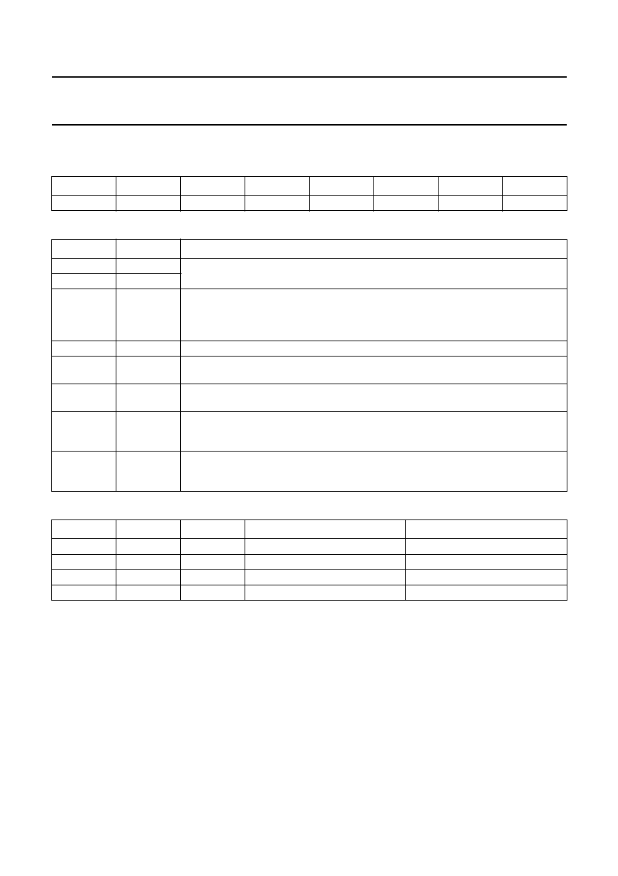
DATA SHEET
Product specification
Supersedes data of 1997 Dec 15
File under Integrated Circuits, IC20
1998 Apr 07
INTEGRATED CIRCUITS
P89C738; P89C739
8-bit Flash microcontrollers

1998 Apr 07
2
Philips Semiconductors
Product specification
8-bit Flash microcontrollers
P89C738; P89C739
CONTENTS
1
FEATURES
2
GENERAL DESCRIPTION
3
ORDERING INFORMATION
4
BLOCK DIAGRAM
5
FUNCTIONAL DIAGRAM
6
PINNING INFORMATION
6.1
Pin configuration
6.2
Pin description
7
FUNCTIONAL DESCRIPTION
7.1
General
7.2
Instruction set execution
8
MEMORY ORGANIZATION
8.1
Program memory
8.2
Internal data memory
8.3
Addressing
9
INTERRUPT SYSTEM
9.1
Interrupt Enable Register (IE)
9.2
Interrupt Priority Register (IP)
10
TIMERS/COUNTERS
10.1
Timer 0 and Timer 1
10.2
Timer 2
10.3
Watchdog Timer (T3)
11
I/O FACILITIES
12
FULL DUPLEX SERIAL PORT (UART)
12.1
The Serial Port operating modes
12.2
Serial Port Control Register (SCON)
13
REDUCED POWER MODES
13.1
Idle mode
13.2
Power-down mode
13.3
Wake-up from Power-down mode
13.4
Status of external pins
13.5
Power Control Register (PCON)
14
OSCILLATOR CIRCUIT
15
RESET
15.1
Power-on reset
16
MULTIPLE PROGRAMMING ROM
(MTP-ROM)
16.1
Features
16.2
General description
16.3
Automatic programming and Automatic chip
erase
16.4
Command definitions
16.5
Silicon-ID-Read command
16.6
Set-up of Automatic chip erase and Automatic
erase commands
16.7
Set-up of the Automatic program and Program
commands
16.8
Reset command
16.9
Write operation status
16.10
Write operation
16.11
System considerations
16.12
Command programming/data programming
and erase operation
17
SPECIAL FUNCTION REGISTERS
OVERVIEW
18
INSTRUCTION SET
19
LIMITING VALUES
20
DC CHARACTERISTICS
21
AC CHARACTERISTICS
21.1
Serial Port characteristics
21.2
Timing waveforms
21.3
Timing symbol naming conventions
22
PACKAGE OUTLINES
23
SOLDERING
23.1
Introduction
23.2
DIP
23.3
PLCC and QFP
24
DEFINITIONS
25
LIFE SUPPORT APPLICATIONS

1998 Apr 07
3
Philips Semiconductors
Product specification
8-bit Flash microcontrollers
P89C738; P89C739
1
FEATURES
∑
80C51 CPU
∑
64-kbyte on-chip Multiple Programming ROM
(MTP-ROM), expandable externally to 64 kbytes
program memory address space
∑
512-byte on-chip RAM, expandable externally to
64 kbytes data memory address space
∑
P89C738 pin outs fully compatible to the standard
8051/8052
∑
8-bit I/O ports for P89C738: 4 and P89C739: 6
∑
Full-duplex UART compatible with the standard 80C51
and the 8052
∑
Two standard 16-bit timers/event counters
∑
An additional 16-bit timer (functionally equivalent to the
Timer 2 of the 8052)
∑
On-chip Watchdog Timer (T3)
∑
6-source and 6-vector interrupt structure with 2 priority
levels
∑
Up to 3 external interrupt request inputs
∑
Two programmable power reduction modes: Idle and
Power-down
∑
Termination of Idle mode by any interrupt, external or
Watchdog Timer reset
∑
Wake-up from Power-down by external interrupt,
external or Watchdog Timer reset
∑
Packages,
≠ P89C738: DIP40, PLCC44 and QFP44
≠ P89C739: PLCC68 and QFP64
∑
Improved Electromagnetic Compatibility (EMC)
∑
Frequency range: 3.5 to 40 MHz
∑
ROM code protection.
2
GENERAL DESCRIPTION
The P89C738 and P89C739 (hereafter generally referred
to as P89C738 unless the P89C739 is specifically
mentioned) are 8 8-bit Flash microcontrollers
manufactured in an advanced CMOS process and is a
derivative of the PCB80C51 microcontroller family. This
device provides architectural enhancements that make it
applicable in a variety of applications in general control
systems, especially in those systems which need a large
on-chip ROM and RAM capacity.
The P89C738 contains a non-volatile 64-kbyte Multiple
Programming ROM (MTP-ROM) program memory, a
volatile 512 bytes read/write data memory, four 8-bit I/O
ports (six for the P89C739), two 16-bit timer/event
counters (identical to the timers of the 80C51), a 16-bit
timer (identical to the Timer 2 of the 8052), a multi-source
two-priority-level nested interrupt structure, one serial
interface (UART), a Watchdog Timer (T3), an on-chip
oscillator and timing circuits. For systems that require
extra capability, the P89C738 can be expanded using
standard TTL compatible memories and logic.
The device also functions as an arithmetic processor
having facilities for both binary and BCD arithmetic plus
bit-handling capabilities. The P89C738 has the same
instruction set as the PCB80C51 which consists of over
100 instructions: 49 one-byte, 46 two-byte and
16 three-byte. With a 16 MHz crystal, 58% of the
instructions are executed in 750 ns and 40% in 1.5
µ
s.
Multiply and divide instructions require 3
µ
s.
3
ORDERING INFORMATION
Notes
1. Temperature and frequency range for all types: 0 to 70
∞
C and 3.5 to 40 MHz.
2. For more information on the package outline of this version, please contact the Philips Semiconductors Sales office.
TYPE
NUMBER
(1)
PACKAGE
NAME
DESCRIPTION
VERSION
P89C738ABA
PLCC44
plastic leaded chip carrier; 44 leads
note 2
P89C738ABP
DIP40
plastic dual in-line package; 40 leads (600 mil)
SOT129-1
P89C738ABB
QFP44
plastic quad flat package; 44 leads
note 2
P89C739ABA
PLCC68
plastic leaded chip carrier; 68 leads
note 2
P89C739ABB
QFP64
plastic quad flat package; 64 leads (lead length 1.95 mm);
body 14
◊
20
◊
2.7 mm; high stand-off height
SOT319-1

1998
Apr
07
4
Philips Semiconductors
Product specification
8-bit Flash microcontrollers
P89C738; P89C739
This text is here in white to force landscape pages to be rotated correctly when browsing through the pdf in the Acrobat reader.This text is here in
_
white to force landscape pages to be rotated correctly when browsing through the pdf in the Acrobat reader.This text is here inThis text is here in
white to force landscape pages to be rotated correctly when browsing through the pdf in the Acrobat reader. white to force landscape pages to be ...
4
BLOCK DIAGRAM
d
book, full pagewidth
MGK189
XTAL2
XTAL1
P3
P2
P1
P0
PARALLEL I/O PORTS
AND
EXTERNAL BUS
WATCHDOG
TIMER
(T3)
TWO 16-BIT
TIMERS/
EVENT
COUNTERS
(T0, T1)
80C51 core
excluding
ROM/RAM
CPU
PROGRAM
MEMORY
64-kbyte
MTP-ROM
16-BIT
TIMER/
EVENT
COUNTER
(T2)
16 kbytes BUS
EXPANSION CONTROL
DATA
MEMORY
256-byte
RAM
DATA
MEMORY
256-byte
AUX-RAM
PROGRAMMABLE
SERIAL PORT
FULL DUPLEX
UART
SYNCHRONOUS
SHIFT
8-bit
internal bus
internal
reset
P89C738
P89C739
8
8
8
8
8
8
P5
(3)
P4
(3)
RST
VDD
VSS
RXD
(2)
TXD
(2)
INT1
(2)
internal
interrupts
INT0
(2)
T1
(2)
T0
(2)
PSEN
EA
ALE/WE
WR
(2)
T2EX
(1)
T2
(1)
RD
(2)
Fig.1 Block diagram.
(1) Alternative function for Port 1.
(2) Alternative function for Port 3.
(3) P4 and P5 are only available on the P89C738ABA and P89C739ABB (PLCC68 and QFP64).

1998 Apr 07
5
Philips Semiconductors
Product specification
8-bit Flash microcontrollers
P89C738; P89C739
5
FUNCTIONAL DIAGRAM
Fig.2 Functional diagram.
handbook, full pagewidth
MGK191
PORT 0
SS
V
DD
V
PORT 1
PORT 3
ADDRESS
AND
DATA BUS
PORT 2
ADDRESS
BUS
secondary
functions
T2
T2EX
PORT 4
PORT 5
RST
XTAL1
XTAL2
RXD
TXD
T0
T1
RD
WR
INT1
INT0
P89C738
P89C739
PSEN
EA
ALE

1998 Apr 07
6
Philips Semiconductors
Product specification
8-bit Flash microcontrollers
P89C738; P89C739
6
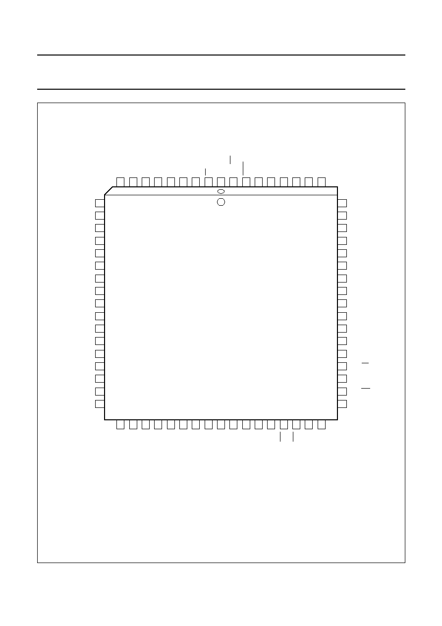
PINNING INFORMATION
6.1
Pin configuration
handbook, full pagewidth
12
13
14
15
16
17
7
8
9
10
11
39
38
37
36
35
34
33
32
31
30
29
18
19
20
21
22
23
24
25
26
27
28
6
5
4
3
2
1
44
43
42
41
40
MGK185
n.c.
P2.7/A15
P2.6/A14
P2.5/A13
P1.5
P1.6
P1.7
RST
P3.0/RXD/data
n.c.
P3.5/T1
EA/VPP
P3.1/TXD/clock
P3.4/T0
P0.4/AD4
P0.5/AD5
P0.6/AD6
P0.7/AD7
P3.2/INT0
P3.3/INT1
PSEN
ALE/WE
n.c.
P2.0/A8
P2.2/A10
P2.3/A11
P2.4/A12
P2.1/A9
V
SS
XTAL2
XTAL1
P3.6/WR
P3.7/RD
n.c.
P1.4
P1.3
P1.2
P1.1/T2EX
P1.0/T2
V
DD
P0.0/AD0
P0.1/AD1
P0.2/AD2
P0.3/AD3
P89C738ABA
Fig.3 Pin configuration for PLCC44 package; for more information on the version see Chapter 3.

1998 Apr 07
7
Philips Semiconductors
Product specification
8-bit Flash microcontrollers
P89C738; P89C739
Fig.4 Pin configuration for DIP40 package (SOT129-1).
handbook, halfpage
P89C738ABP
MGK184
1
2
3
4
5
6
7
8
9
10
11
12
13
14
15
16
17
18
19
20
40
39
38
37
36
35
34
33
32
31
30
29
28
27
26
25
24
23
22
21
VDD
P0.0/AD0
P0.1/AD1
P0.2/AD2
P0.3/AD3
P0.4/AD4
P0.5/AD5
P0.6/AD6
P0.7/AD7
P2.6/A14
P2.5/A13
P2.4/A12
P2.3/A11
P2.2/A10
P2.1/A9
P2.7/A15
P2.0/A8
P1.0/T2
P1.1/T2EX
P1.2
P1.3
P1.4
P1.5
P1.6
P1.7
P3.0/RXD/data
P3.1/TXD/clock
P3.4/T0
P3.5/T1
RST
XTAL2
XTAL1
VSS
P3.2/INT0
EA/VPP
ALE/WE
PSEN
P3.6/WR
P3.3/INT1
P3.7/RD

1998 Apr 07
8
Philips Semiconductors
Product specification
8-bit Flash microcontrollers
P89C738; P89C739
Fig.5 Pin configuration for QFP44 package; for more information on the version see Chapter 3.
handbook, full pagewidth
1
2
3
4
5
6
7
8
9
10
11
33
32
31
30
29
28
27
26
25
24
23
12
13
14
15
16
17
18
19
20
21
22
44
43
42
41
40
39
38
37
36
35
34
MGK186
n.c.
P2.7/A15
P2.6/A14
P2.5/A13
P1.5
P1.6
P1.7
RST
P3.0/RXD/data
n.c.
P3.5/T1
EA/VPP
n.c.
P2.0/A8
P2.2/A10
P2.3/A11
P2.4/A12
P2.1/A9
n.c.
P1.4
P1.3
P1.2
P1.1/T2EX
P1.0/T2
P3.1/TXD/clock
P3.4/T0
P89C738ABB
V
DD
P0.0/AD0
P0.1/AD1
P0.2/AD2
P0.3/AD3
P0.4/AD4
P0.5/AD5
P0.6/AD6
P0.7/AD7
V
SS
XTAL2
XTAL1
P3.2/INT0
P3.3/INT1
PSEN
ALE/WE
P3.6/WR
P3.7/RD
1998 Apr 07
9
Philips Semiconductors
Product specification
8-bit Flash microcontrollers
P89C738; P89C739
Fig.6 Pin configuration for PLCC68 package; for more information on the version see Chapter 3.
handbook, full pagewidth
P89C739ABA
MGK187
10
11
12
13
14
15
16
17
18
19
20
21
22
23
24
25
26
P5.5
P5.6
P5.7
P1.0/T2
P4.0
P1.1/T2EX
P1.2
P1.3
P4.1
P1.4
P4.2
60
59
58
57
56
55
54
53
52
51
50
49
48
47
46
45
44
P5.0
P2.4/AD12
P2.3/AD11
P4.7
P2.2/AD10
P2.1/AD9
P2.0/AD8
P4.6
P4.5
P4.4
P4.3
27
28
29
30
31
32
33
34
35
36
37
38
39
40
41
42
43
P1.5
P1.6
P1.7
RST
P3.0/RXD/data
n.c.
n.c.
n.c.
n.c.
n.c.
n.c.
n.c.
n.c.
n.c.
n.c.
P3.1/TXD/clock
P3.2/INT0
P3.3/INT1
P3.4/T0
P3.5/T1
9
8
7
6
5
4
3
2
1
68
67
66
65
64
63
62
61
P0.4/AD4
P5.4
P5.3
P0.5/AD5
P0.6/AD6
P0.7/AD7
P2.7/AD15
P2.6/AD14
P5.2
P5.1
P2.5/AD13
P0.0/AD0
P0.1/AD1
P0.2/AD2
P0.3/AD3
n.c.
XTAL2
XTAL1
VSS
VDD
n.c.
EA/V
PP
ALE/WE
PSEN
P3.7/RD
P3.6/WR

1998 Apr 07
10
Philips Semiconductors
Product specification
8-bit Flash microcontrollers
P89C738; P89C739
Fig.7 Pin configuration for QFP64 package (SOT319-1).
handbook, full pagewidth
MGK188
1
2
3
4
5
6
7
8
9
10
11
12
13
14
15
16
17
18
19
P0.4/AD4
P1.5
P2.5/AD13
P3.5/T1
51
50
49
48
47
46
45
44
43
42
41
40
39
38
37
36
35
34
33
20
21
22
23
24
25
26
27
28
29
30
31
32
64
63
62
61
60
59
58
57
56
55
54
53
52
P89C739ABB
P5.5
P5.6
P5.7
P1.0/T2
P4.0
P1.1/T2EX
P1.2
P1.3
P4.1
P1.4
P4.2
P5.0
P2.4/AD12
P2.3/AD11
P4.7
P2.2/AD10
P2.1/AD9
P2.0/AD8
P4.6
P4.5
P4.4
P4.3
P1.6
P1.7
RST
P3.0/RXD/data
n.c.
n.c.
n.c.
n.c.
n.c.
P3.1/TXD/clock
P3.2/INT0
P3.3/INT1
P3.4/T0
P0.0/AD0
P0.1/AD1
P0.2/AD2
P0.3/AD3
n.c.
XTAL2
XTAL1
VSS
VDD
VSS
P3.7/RD
P3.6/WR
n.c.
P5.3
P5.4
P0.5/AD5
P0.6/AD6
P0.7/AD7
P2.7/AD15
P2.6/AD14
P5.1
P5.2
EA/V
PP
ALE/WE
PSEN

1998
Apr
07
11
Philips Semiconductors
Product specification
8-bit Flash microcontrollers
P89C738; P89C739
This text is here in white to force landscape pages to be rotated correctly when browsing through the pdf in the Acrobat reader.This text is here in
_
white to force landscape pages to be rotated correctly when browsing through the pdf in the Acrobat reader.This text is here inThis text is here in
white to force landscape pages to be rotated correctly when browsing through the pdf in the Acrobat reader. white to force landscape pages to be ...
6.2
Pin description
Table 1
Pin description for DIP40; QFP44; PLC44; QFP64 and PLCC68.
SYMBOL
PIN
(1)
DESCRIPTION
PLCC68
QFP64
PLCC44
QFP44
DIP40
P1.0/T2
19
11
16
2
1
Port 1: P1.0 to P1.7; 8-bit quasi-bidirectional I/O port. Port 1 can
sink/source one TTL (= 4 LSTTL) input. It can drive CMOS inputs
without external pull-ups.
Port 1 alternative functions are: T2; Timer/event counter 2 external
event counter input (falling edge triggered). T2EX; Timer/event
counter 2 capture/reload trigger or external interrupt 2 input (falling
edge triggered).
P1.1/T2EX
21
13
15
3
2
P1.2
22
14
14
4
3
P1.3
23
15
13
5
4
P1.4
25
17
12
6
5
P1.5
27
19
1
7
6
P1.6
28
20
2
8
7
P1.7
29
21
3
9
8
RST
30
22
4
10
9
Reset; a HIGH level on this pin for two machine cycles while the
oscillator is running, resets the device. An internal pull-down resistor
permits power-on reset using only a capacitor connected to V
DD
.
After a Watchdog Timer overflow this pin is pulled HIGH while the
internal reset signal is active.
P3.0/RXD/data
34
26
5
11
10
Port 3: P3.0 to P3.7; 8-bit quasi-bidirectional I/O Port with internal
pull-ups. Port 3 can sink/source one TTL (= 4 LSTTL) input. It can
drive CMOS inputs without external pull-ups.
Port 3 alternative functions are: RXD/data; Serial Port data input
(asynchronous) or data input/output (synchronous).
TXD/clock; Serial Port data output (asynchronous) or clock output
(synchronous). INT0; External interrupt 0 or gate control input for
Timer/event counter 0. INT1; External interrupt 1 or gate control
input for Timer/event counter 1. T0; external input for Timer/event
counter 0. T1; external input for Timer/event counter 1.
WR; external data memory write strobe. RD; external data memory
read strobe.
P3.1/TXD/clock 39
29
7
13
11
P3.2/INT0
40
30
8
14
12
P3.3/INT1
41
31
9
15
13
P3.4/T0
42
32
10
16
14
P3.5/T1
43
33
11
17
15
P3.6WR
45
35
44
18
16
P3.7/RD
47
37
43
19
17
XTAL2
48
38
42
20
18
Crystal input 2: output of the inverting amplifier that forms the
oscillator. This pin left open-circuit when an external oscillator clock
is used (see Figs 18 and 20).
XTAL1
49
39
41
21
19
Crystal input 1: input to the inverting amplifier that forms the
oscillator, and input to the internal clock generator. Receives the
external oscillator clock signal when an external oscillator is used
(see Figs 18 and 20).
V
SS
51
41
40
22
20
Ground: circuit ground potential.
1998
Apr
07
12
Philips Semiconductors
Product specification
8-bit Flash microcontrollers
P89C738; P89C739
P2.0/A8 to
P2.2/A10
54 to 56
44 to 46
38 to 34
24 to 31
21 to 28
Port 2: P2.0 to P2.7; 8-bit quasi-bidirectional I/O Port with internal
pull-ups. Port 2 can sink/source one TTL (= 4 LSTTL) input. It can
drive CMOS inputs without external pull-ups.
Port 2 alternative functions are: A8 to A15; during access to
external memories (RAM/ROM) that use 16-bit addresses (MOVX
@DPTR) Port 2 emits the high-order address byte (A8 to A15).
P2.3/A11 to
P2.4/A12
58 to 59
48 to 49
P2.5/A13 to
P2.7/A15
61, 64
and 65
51, 54
and 55
23 to 25
PSEN
67
56
26
32
29
Program Store Enable output: read strobe to the external program
memory via Port 0 and Port 2. It is activated twice each machine
cycle during fetches from external program memory.
When executing out of external program memory two activations of
PSEN are skipped during each access to external data memory.
PSEN is not activated (remains HIGH) during no fetches from
external program memory. PSEN can sink/source 8 LSTTL inputs. It
can drive CMOS inputs without external pull-ups.
ALE/WE
(2)
68
57
27
33
30
Address Latch Enable output: latches the lower byte of the
address during access to external memory in normal operation. It is
activated every six oscillator periods except during an external data
memory access. ALE can sink/source 8 LSTTL inputs. It can drive
CMOS inputs without an external pull-up.
WE: Write Enable.
EA/V
PP
2
59
29
35
31
External Access input: when during reset, EA is held at a TTL
HIGH level, the CPU executes from the internal program ROM.
When EA is held at a TTL LOW level during reset, the CPU executes
out of external program memory via Port 0 and Port 2. EA is not
allowed to float. EA is latched during reset and don't care after reset.
V
PP
: programming supply voltage.
P0.7/AD7 to
P0.4/AD4
3, 5, 6
and 9
60, 61, 62
and 1
30 to 33
36 to 43
32 to 39
Port 0: P0.7 to P0.0; 8-bit open-drain bidirectional I/O port. It is also
the multiplexed low-order address and data bus during accesses to
external memory: AD0 to AD7. During these accesses internal
pull-ups are activated. Port 0 can sink/source 8 LSTTL inputs.
P0.3/AD3 to
P0.2/AD2
11 to 12
3 to 4
22 to 21
P0.1/AD1 to
P0.0/AD0
14 to 15
6 to 7
20 to 19
V
DD
17
9
18
44
40
Power supply (+5 V) pin for normal operation, Idle mode and
Power-down mode.
SYMBOL
PIN
(1)
DESCRIPTION
PLCC68
QFP64
PLCC44
QFP44
DIP40

1998
Apr
07
13
Philips Semiconductors
Product specification
8-bit Flash microcontrollers
P89C738; P89C739
Notes
1. To avoid a `latch-up' effect at power-on, the voltage on any pin (at any time) must not be higher than V
DD
+ 0.5 V or lower than V
SS
-
0.5 V
respectively.
2. To prohibit the toggling of the ALE/WE pin (RFI noise reduction) the bit RFI in the PCON register (PCON.5) must be set by software. This bit is
cleared on reset and can be cleared by software. When set, ALE/WE pin will be pulled down internally, switching an external address latch to a
quiet state. The MOVX instruction will still toggle ALE/WE as a normal MOVX. ALE/WE will retain its normal HIGH value during Idle mode and a
LOW value during Power-down mode while in the `RFI' mode. Additionally during internal access (EA = 1) ALE/WE will toggle normally when the
address exceeds the internal program memory size. During external access (EA = 0) ALE/WE will always toggle normally, whether the flag `RFI' is
set or not.
3. n.a. = not applicable.
P4.0 to P4.7
20, 24,
26, 44,
46, 50, 53
and 57
12, 16,
18, 34,
36, 40, 43
and 47
n.a.
(3)
n.a.
n.a.
Port 4: P4.0 to P4.7; 8-bit quasi-bidirectional I/O port with internal
pull-ups. Port 4 can sink/source 4 LSTTL inputs. It can drive CMOS
inputs without external pull-ups.
P5.0 to P5.7
60, 62,
63, 7, 8,
10, 13
and 16
50, 52,
53, 63,
64, 2, 5
and 8
n.a.
n.a.
n.a.
Port 5: P5.0 to P5.7; 8-bit quasi-bidirectional I/O port with internal
pull-ups. Port 5 can sink/source 4 LSTTL inputs. It can drive CMOS
inputs without external pull-ups.
n.c.
1, 4, 18,
31, 32,
33, 35,
36, 37, 38
52 and 66
23, 24,
25, 27,
28, 42
and 58
6, 17, 28
and 39
1, 12, 23
and 34
n.a.
Not connected.
SYMBOL
PIN
(1)
DESCRIPTION
PLCC68
QFP64
PLCC44
QFP44
DIP40

1998 Apr 07
14
Philips Semiconductors
Product specification
8-bit Flash microcontrollers
P89C738; P89C739
7
FUNCTIONAL DESCRIPTION
This chapter gives a brief overview of the device.
Detailed functional descriptions are given in the following
chapters:
Chapter 8 "Memory organization"
Chapter 9 "Interrupt system"
Chapter 10 "Timers/counters"
Chapter 11 "I/O facilities"
Chapter 12 "Full duplex Serial Port (UART)"
Chapter 13 "Reduced power modes"
Chapter 14 "Oscillator circuit"
Chapter 15 "Reset"
Chapter 16 "Multiple Programming ROM (MTP-ROM)".
7.1
General
The P89C738 is a stand-alone high-performance
microcontroller designed for use in real time applications
such as instrumentation, industrial control and medium to
high-end consumer applications.
In addition to the 80C51 standard functions, the device
provides a number of dedicated hardware functions for
these applications. The P89C738 is a control-oriented
CPU with on-chip Program and data memory. It can
execute programs with internal or external program
memory up to 64 kbytes. It can also access up to
64 kbytes of external data memory. For systems requiring
extra capability, the P89C738 can be expanded using
standard memories and peripherals.
The P89C738 has two software selectable modes of
reduced activity for further power reduction: Idle and
Power-down. The Idle mode freezes the CPU while
allowing the RAM, timers, serial ports and interrupt system
to continue functioning. The Power-down mode saves the
RAM contents but freezes the oscillator causing all other
chip functions to be inoperative except the Watchdog
Timer if it is enabled. The Power-down mode can be
terminated by an external reset, a Watchdog Timer
overflow and in addition, by either of the two external
interrupts.
7.2
Instruction set execution
The P89C738 uses the powerful instruction set of the
80C51. Additional Special Function Registers (SFRs) are
incorporated to control the on-chip peripherals.
The instruction set consists of 49 single-byte, 46 two-byte
and 16 three-byte instructions. When using a 16 MHz
oscillator, 64 instructions execute in 750 ns and
45 instructions execute in 1.5
µ
s. Multiply and divide
instructions execute in 3
µ
s (see Chapter 18).

1998 Apr 07
15
Philips Semiconductors
Product specification
8-bit Flash microcontrollers
P89C738; P89C739
8
MEMORY ORGANIZATION
The Central Processing Unit (CPU) manipulates operands
in three memory spaces; these are the 64 kbytes external
data memory (of which the lower 256 bytes reside in the
internal AUX-RAM), 512 bytes internal data memory
(consisting of 256 bytes standard RAM and 256 bytes
AUX-RAM) and the 64 kbytes internal and external
program memory.
8.1
Program memory
The program memory address space of the P89C738
comprises an internal and an external memory portion.
The P89C738 has 64 kbytes of program memory on-chip.
The program memory can also be externally addressed up
to 64 kbytes. If the EA pin is held HIGH, the P89C738
executes out of the internal program memory. If EA pin is
held LOW, the P89C738 fetches all instructions from the
external program memory. Figure 8 illustrates the program
memory address space.
The security bit is always set in the P89C738 and
P89C739 to protect the ROM code. Table 2 lists the
access to the internal and external program memory by the
MOVC instructions when the security bit has been set to a
logic 1. If the security bit has been set to a logic 0 there are
no restrictions for the MOVC instructions.
Table 2
Internal and external program memory access
MOVC
INSTRUCTION
PROGRAM MEMORY ACCESS
INTERNAL
EXTERNAL
MOVC in internal
program memory
YES
YES
MOVC in external
program memory
NO
YES
Fig.8 Program memory address space.
handbook, halfpage
MGK190
EXTERNAL
(EA = 0)
INTERNAL
(EA = 1)
PROGRAM MEMORY
65535
0
8.2
Internal data memory
The internal data memory is divided into three physically
separated parts: 256 bytes of RAM, 256 bytes of
AUX-RAM, and a 128 bytes Special Function Registers
(SFRs) area. These parts can be addressed as follows
(see Fig.9 and Table 3):
∑
RAM locations 0 to 127 can be addressed directly and
indirectly as in the 80C51. Address pointers are R0 and
R1 of the selected register bank.
∑
RAM locations 128 to 255 can only be addressed
indirectly. Address pointers are R0 and R1 of the
selected register bank.
∑
AUX-RAM locations 0 to 255 are indirectly addressable
as the external data memory locations 0 to 255 with the
MOVX instructions. Address pointers are R0 and R1 of
the selected register bank and DPTR. When executing
from internal program memory, an access to AUX-RAM
0 to 255 will not affect the ports Port 0, Port 2,
P3.6 and P3.7.
∑
The SFRs can only be addressed directly in the address
range from 128 to 255.
An access to external data memory locations higher than
255 will be performed with the MOVX DPTR instructions in
the same way as in the 80C51 structure, i.e. with Port 0
and Port 2 as data/address bus and P3.6 and P3.7 as write
and read timing signals. Note that the external data
memory cannot be accessed with R0 and R1 as address
pointer.
Figure 9 shows the internal and external data memory
address space. Chapter 17 shows the Special Function
Registers overview. Four 8-bit register banks occupy
locations 0 through 31 in the lower RAM area. Only one of
these banks may be enabled at a time. The next 16 bytes,
locations 32 through 47, contain 128 directly addressable
bit locations.
The stack can be located anywhere in the internal
256-byte RAM. The stack depth is only limited by the
available internal RAM space of 256 bytes. All registers
except the Program Counter and the four 8-bit register
banks reside in the SFR address space.
Table 3
Internal data memory access
MEMORY
LOCATION
ADDRESS MODE
RAM
0 to 127
direct and indirect
128 to 255
indirect only
SFR
128 to 255
direct only
AUX-RAM
0 to 255
indirect only with MOVX

1998 Apr 07
16
Philips Semiconductors
Product specification
8-bit Flash microcontrollers
P89C738; P89C739
Fig.9 Internal and external data memory address space.
handbook, full pagewidth
MBK524
INDIRECT ONLY
DIRECT AND
INDIRECT
AUXILIARY
RAM
SFRs
255
127
0
EXTERNAL
(EA = 0)
INTERNAL
(EA = 1)
MAIN RAM
INTERNAL DATA MEMORY
EXTERNAL
DATA MEMORY
PROGRAM MEMORY
64 kbytes
64 kbytes
64 kbytes
0
OVERLAPPED SPACE
256
8.3
Addressing
The P89C738 has five modes for addressing:
∑
Register
∑
Direct
∑
Register-Indirect
∑
Immediate
∑
Base-Register plus Index-Register-Indirect.
The first three methods can be used for addressing
destination operands. Most instructions have a
`destination/source' field that specifies the data type,
addressing methods and operands involved.
For operations other than MOVs, the destination operand
is also a source operand.
Access to memory addresses is as follows:
∑
Register in one of the four 8-bit register banks through
Register, Direct or Register-Indirect addressing
∑
512 bytes of internal RAM through Direct or
Register-Indirect addressing. Bytes 0 to 127 of internal
RAM may be addressed directly/indirectly. Bytes
128 to 255 of internal RAM share their address location
with the SFRs and so may only be addressed indirectly
as data RAM. Bytes 0 to 255 of AUX-RAM can only be
addressed indirectly via MOVX.
∑
SFR through Direct addressing at address locations
128 to 255
∑
External data memory through Register-Indirect
addressing
∑
Program memory look-up tables through Base-Register
plus Index-Register-Indirect addressing.

1998 Apr 07
17
Philips Semiconductors
Product specification
8-bit Flash microcontrollers
P89C738; P89C739
9
INTERRUPT SYSTEM
The P89C738 contains the same interrupt structure as the
PCB80C51BH, but with a six-source interrupt structure
with two priority levels (see Fig.10).
The external interrupts INT0 and INT1 can each be either
level-activated or transition-activated, depending on bits
IT0 and IT1 in SFR TCON. The flags that actually generate
these interrupts are bits IE0 and IE1 in TCON. When an
external interrupt is generated, the corresponding request
flag is cleared by the hardware when the service routine is
vectored to, only if the interrupt was transition-activated.
If the interrupt was level-activated the external source has
to hold the request active until the requested interrupt is
actually generated. Then it has to deactivate the request
before the interrupt service routine is completed, or else
another interrupt will be generated.
The Timer 0 and Timer 1 interrupts are generated by TF0
and TF1, which are set by a roll-over in their respective
timer/counter register (except for Timer 0 in Mode 3 of the
serial interface). When a timer interrupt is generated, the
flag that generated it is cleared by the on-chip hardware
when the service routine is vectored to.
The Serial Port interrupt is generated by the logical `OR' of
RI and TI. Neither of these flags is cleared by hardware.
The service routine will normally have to determine
whether it was RI or TI that generated the interrupt, and the
bit will have to be cleared by software.
The Timer 2 interrupt is generated by the logical OR of TF2
and EXF2. Neither of these flags is cleared by hardware.
In fact the service routine may have to determine whether
it was TF2 or EXF2 that generated the interrupt, and the bit
will have to be cleared by software.
An additional (third) external interrupt is available, if
Timer 2 is not used as timer/counter or if Timer 2 is used
in the baud rate generator mode. That external interrupt 2
is falling-edge triggered. It shares the Timer 2 interrupt
vector, interrupt enable and interrupt priority bits. If bit
EXEN2 = 1 (T2CON.3), a HIGH-to-LOW transition at pin
P1.1/T2EX sets the interrupt request flag EXF2
(T2CON.6) and can be used to generate an external
interrupt.
The interrupt vectors are listed in Table 4.
Table 4
Interrupt vectors
SOURCE
PRIORITY
WITHIN LEVEL
VECTOR
ADDRESS
IE0
1 (highest)
0003H
TF0
2
000BH
IE1
3
0013H
TF1
4
001BH
RI + TI
5
0023H
TF2 + EXF2
6 (lowest)
002BH
Fig.10 P89C738/P89C739 interrupt sources.
handbook, halfpage
MGK193
IT1
INT1
TF1
TF0
TI
RI
TF2
EXF2
IE1
IT0
INT0
IE0
1
0
interrupt
sources
1
0

1998 Apr 07
18
Philips Semiconductors
Product specification
8-bit Flash microcontrollers
P89C738; P89C739
9.1
Interrupt Enable Register (IE)
Table 5
Interrupt Enable Register (SFR address A8H)
Table 6
Description of IE bits
9.2
Interrupt Priority Register (IP)
Table 7
Interrupt Priority Register (SFR address B8H)
Table 8
Description of IP bits
7
6
5
4
3
2
1
0
EA
-
ET2
ES
ET1
EX1
ET0
EX0
BIT
SYMBOL
DESCRIPTION
7
EA
General enable/disable control. If EA = 0, no interrupt is enabled. If EA = 1, any
individually enabled interrupt will be accepted.
6
-
reserved
5
ET2
enable Timer 2 interrupt
4
ES
enable Serial Port interrupt
3
ET1
enable Timer 1 interrupt
2
EX1
enable external interrupt 1
1
ET0
enable Timer 0 interrupt
0
EX0
enable external interrupt 0
7
6
5
4
3
2
1
0
-
-
PT2
PS
PT1
PX1
PT0
PX0
BIT
SYMBOL
DESCRIPTION
7
-
reserved
6
-
reserved
5
PT2
Timer 2 interrupt priority level
4
PS
Serial Port interrupt priority level
3
PT1
Timer 1 interrupt priority level
2
PX1
external interrupt 1 priority level
1
PT0
Timer 0 interrupt priority level
0
PX0
external interrupt 0 priority level
1998 Apr 07
19
Philips Semiconductors
Product specification
8-bit Flash microcontrollers
P89C738; P89C739
10 TIMERS/COUNTERS
The P89C738 contains three 16-bit timer/counters:
Timer 0, Timer 1 and Timer 2; and one 8-bit timer, the
Watchdog Timer (T3). Timer 0, Timer 1 and Timer 2 may
be programmed to carry out the following functions:
∑
Measure time intervals and pulse durations
∑
Count events
∑
Generate interrupt requests.
10.1
Timer 0 and Timer 1
Timers 0 and 1 each have a control bit in SFR TMOD that
selects the timer or counter function of the corresponding
timer. In the timer function, the register is incremented
every machine cycle. Thus, one can think of it as counting
machine cycles. Since a machine cycle consists
of 12 oscillator periods, the count rate is
1
/
12
of the
oscillator frequency.
In the counter function, the register is incremented in
response to a HIGH-to-LOW transition at the
corresponding external input pin, T0 or T1. In this function,
the external input is sampled during S5P2 of every
machine cycle. When the samples show a HIGH in one
cycle and a LOW in the next cycle, the counter is
incremented. Thus, it takes two machine cycles
(24 oscillator periods) to recognize a HIGH-to-LOW
transition. There are no restrictions on the duty cycle of the
external input signal, but to ensure that a given level is
sampled at least once before it changes, it should be held
for at least one full machine cycle.
Timer 0 and Timer 1 can be programmed independently to
operate in one of four modes:
Mode 0 8-bit timer/counter with divide-by-32 prescaler
Mode 1 16-bit timer/counter
Mode 2 8-bit timer/counter with automatic reload
Mode 3 Timer 0: one 8-bit timer/counter and one 8-bit
timer. Timer 1: stopped.
When Timer 0 is in Mode 3, Timer 1 can be programmed
to operate in Modes 0, 1 or 2 but cannot set an interrupt
request flag and generate an interrupt. However, the
overflow from Timer 1 can be used to pulse the Serial Port
transmission-rate generator. With a 16 MHz crystal, the
counting frequency of these timer/counters is as follows:
∑
In the timer function, the timer is incremented at a
frequency of 1.33 MHz (
1
/
12
◊
oscillator frequency)
∑
In the counter function, the frequency handling range for
external inputs is 0 to 0.66 MHz.
Both internal and external inputs can be gated to the timer
by a second external source for directly measuring pulse
duration.
The timers are started and stopped under software control.
Each one sets its interrupt request flag when it overflows
from all logic 1's to all logic 0's (respectively, the automatic
reload value), with the exception of Mode 3 as previously
described.
10.1.1
Timer/Counter Mode Control Register (TMOD)
Table 9
Timer/Counter Mode Control Register (SFR address 89H)
Table 10 Description of TMOD bits for Timer 1 and Timer 0
Timer 0: bit TMOD.0 to TMOD.3; Timer 1: bit TMOD.4 to TMOD.7; n = 0, 1.
7
6
5
4
3
2
1
0
GATE
C/T
M1
M0
GATE
C/T
M1
M0
BIT
SYMBOL
DESCRIPTION
7 and 3
GATE
Gating control. When set Timer/counter `n' is enabled only when INTn pin is HIGH and
control bit TRn (TR1 or TR0) is set. When cleared Timer n is enabled whenever TRn
control bit is set.
6 and 2
C/T
Timer or Counter Selector. Cleared for Timer operation; input from internal system
clock. Set for Counter operation; input from pin Tn (T1 or T0).
5 and 1
M1
Timer 0, Timer 1 mode select; see Table 11.
4 and 0
M0

1998 Apr 07
20
Philips Semiconductors
Product specification
8-bit Flash microcontrollers
P89C738; P89C739
Table 11 Timer 0; Timer 1 mode select
10.1.2
Timer/Counter Control Register (TCON)
Table 12 Timer/Counter Control Register (SFR address 88H)
Table 13 Description of TCON bits
M1
M0
OPERATING
0
0
Timer TL0; TL1 serves as 5-bit prescaler.
0
1
16-bit Timer/Counter TH0; TH1 and TL0; TL1 are cascaded; there is no prescaler.
1
0
8-bit auto-reload Timer/Counter TH0; TH1 holds a value which is to be reloaded into
TL0; TL1 each time it overflows.
1
1
Timer 0: TL0 is an 8-bit Timer/Counter controlled by the standard Timer 0 control bits.
TH0 is an 8-bit timer only controlled by Timer 1 control bits.
1
1
Timer 1: Timer/Counter 1 stopped.
7
6
5
4
3
2
1
0
TF1
TR1
TF0
TR0
IE1
IT1
IE0
IT0
BIT
SYMBOL
DESCRIPTION
7 and 5
TF1 and TF0 Timer 1 and Timer 0 overflow flags. Set by hardware on Timer/Counter overflow.
Cleared by hardware when processor vectors to interrupt routine.
6 and 4
TR1 and TR0 Timer 1 and Timer 0 run control bits. Set/cleared by software to turn Timer/Counter
on/off.
3 and 1
IE1 and IE0
Interrupt 1 and Interrupt 0 edge flags. Set by hardware when external interrupt edge
detected. Cleared when interrupt processed.
2 and 0
IT1 and IT0
Interrupt 1 and Interrupt 0 type control bits. Set/cleared by software to specify falling
edge/LOW level triggered external interrupts.

1998 Apr 07
21
Philips Semiconductors
Product specification
8-bit Flash microcontrollers
P89C738; P89C739
10.2
Timer 2
Timer 2 is functionally similar to the Timer 2 of the 8052AH. Timer 2 is a 16-bit timer/counter which is formed by two
SFRs, TL2 and TH2. Another pair of SFRs, RCAP2L and RCAP2H, form a 16-bit capture register or a 16-bit reload
register.
Like Timer 0 and Timer 1, Timer 2 can operate either as timer or as event counter. This is selected by bit C/T2 in SFR
T2CON. The timer has three operating modes: `capture', `autoload' and `baud rate generator', which are selected by bits
in SFR T2CON (see Tables 14 and 15).
10.2.1
T
IMER
/C
OUNTER
2 C
ONTROL
R
EGISTER
(T2CON)
Table 14 Timer/Counter 2 Control Register (SFR address C8H)
Table 15 Description of T2CON bits
Table 16 Timer 2 operating modes
X = don't care.
7
6
5
4
3
2
1
0
TF2
EXF2
RCLK
TCLK
EXEN2
TR2
C/T2
CP/RL2
BIT
SYMBOL
DESCRIPTION
7
TF2
Timer 2 overflow flag. Set by a Timer 2 overflow and must be cleared by software. TF2
will not be set when either RCLK = 1 or TCLK = 1. When Timer 2 interrupt is enabled,
TF2 = 1 will cause the CPU to vector to Timer 2 interrupt routine.
6
EXF2
Timer 2 external flag. Set when either a capture or reload is caused by a negative
transition on T2EX and when EXEN2 = 1. When Timer T2 interrupt is enabled,
EXF2 = 1 will cause the CPU to vector to Timer 2 interrupt routine.
5
RCLK
Receive clock flag. When set, causes the Serial Port to use Timer 2 overflow pulses
for its receive clock in Modes 1 and 3. RCLK = 0 causes Timer 1 overflows to be used
for the receive clock.
4
TCLK
Transmit clock flag. When set, causes the Serial Port to use Timer 2 overflow pulses
for its transmit clock in Modes 1 and 3. TCLK = 0 causes Timer 1 overflows to be used
for the transmit clock.
3
EXEN2
Timer 2 external enable flag. When set, allows a capture or reload to occur as a result
of a negative transition on T2EX, if Timer 2 is not being used to clock the Serial Port.
EXEN2 = 0, causes Timer 2 to ignore events at T2EX.
2
TR2
Timer 2 start/stop control. TR2 = 1 starts Timer 2; TR2 = 0 stops Timer 2.
1
C/T2
Timer 2 timer or counter select. C/T2 = 0 selects the internal timer with a clock
frequency of
1
/
12
f
clk
. C/T2 = 1 selects the external event counter; falling edge triggered.
0
CP/RL2
Capture/reload flag. When set, capture will occur on negative transitions at T2EX if
EXEN2 = 1. When cleared, reloads will occur upon either Timer 2 overflows or negative
transitions at T2EX if EXEN2 = 1. When either RCLK = 1 or TCLK = 1, this bit is ignored
and the timer is forced to reload upon overflow.
RCLK
TCLK
CP/RL2
TR2
MODE
0
0
0
1
16-bit automatic reload
0
0
1
1
16-bit capture
1
1
X
1
baud rate generator
X
X
X
0
off
1998 Apr 07
22
Philips Semiconductors
Product specification
8-bit Flash microcontrollers
P89C738; P89C739
10.2.2
C
APTURE MODE
In the capture mode (see Fig.11) there are two options
which are selected by bit EXEN2 in T2CON. If EXEN2 = 0,
then Timer 2 is a 16-bit timer/counter which on overflow
sets bit TF2 (Timer 2 overflow bit). TF2 can be used to
generate an interrupt. If EXEN2 = 1, Timer 2 operates as
above, with the added feature that a HIGH-to-LOW
transition at the external input T2EX causes the current
value in Timer 2 registers (TL2 and TH2) to be captured
into registers RCAP2L and RCAP2H, respectively. The
HIGH-to-LOW transition of T2EX also causes bit EXF2 in
T2CON to be set. EXF2 can be used to generate an
interrupt.
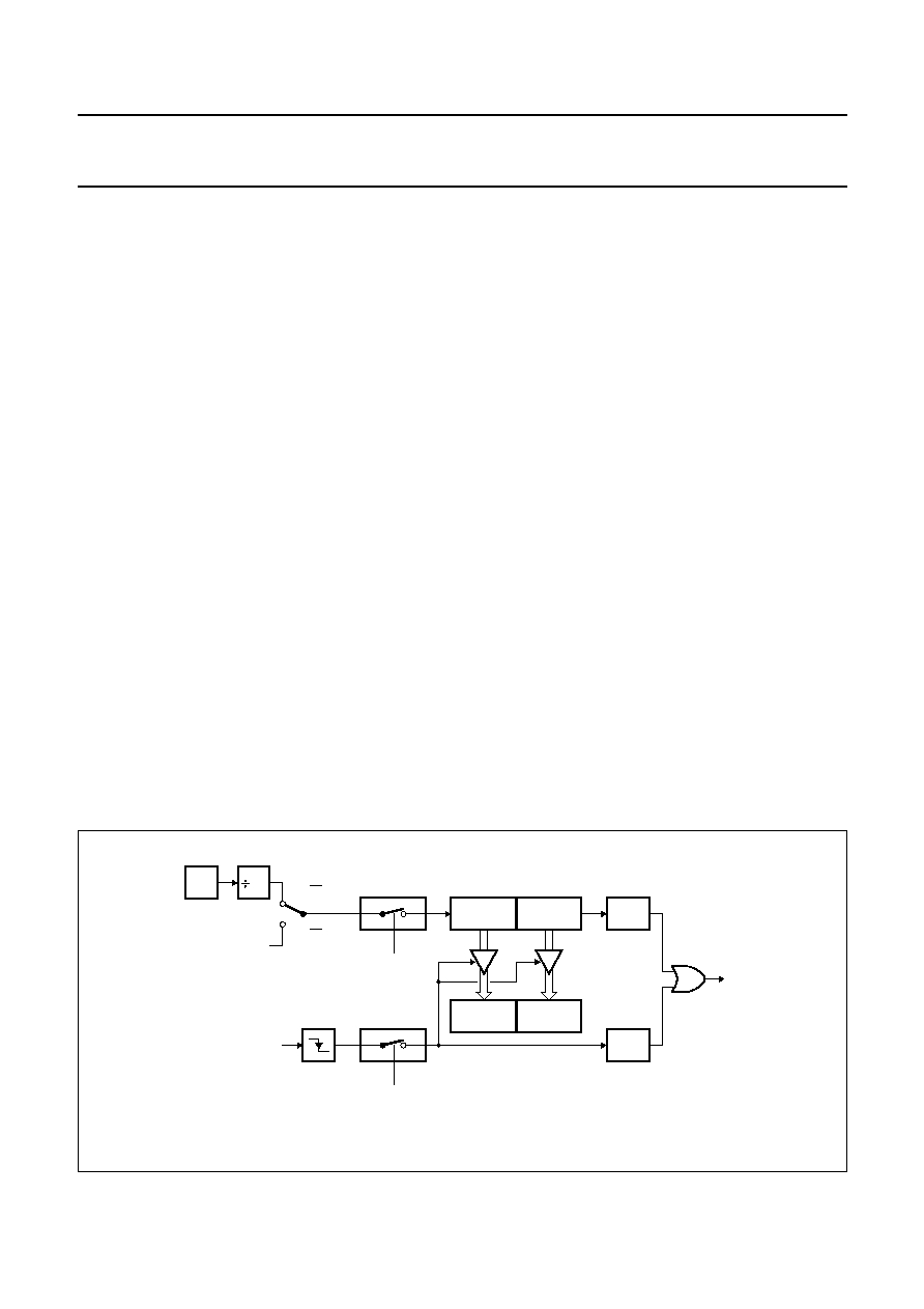
10.2.3
A
UTOMATIC RELOAD MODE
In the automatic reload mode (see Fig.12) there are two
options which are selected by bit EXEN2 in SFR T2CON.
If EXEN2 = 0, then a Timer 2 overflow sets TF2 and
causes the Timer 2 registers to be reloaded with the 16-bit
value in registers RCAP2L and RCAP2H, which are preset
by software.
If EXEN2 = 1, Timer 2 operates as above, with the added
feature that a HIGH-to-LOW transition at the external input
T2EX triggers the 16-bit reload and sets EXF2.
10.2.4
B
AUD RATE GENERATOR MODE
The baud rate generator mode (see Fig.13) is selected by
RCLK = 1 and/or TCLK = 1 in SFR T2CON. Overflows of
either Timer 2 or Timer 1 can be used independently for
generating baud rates for transmit and receive.
The baud rate generation by Timer 1 and/or Timer 2 is
used for the Serial Port in Mode 1 and Mode 3. The baud
rate generation mode is similar to the automatic reload
mode, in that a roll-over in TH2 causes the Timer 2
registers to be reloaded with the 16-bit value in registers
RCAP2L and RCAP2H, which are preset by software.
The baud rates for the Serial Port in Modes 1 and 3 are
determined by Timer 2 overflow rate as follows:
Timer 2 can be configured for either `timer' or `counter'
operation. Normally, as a timer it would increment every
machine cycle (thus at
1
/
12
f
clk
). As a baud rate generator,
however it increments every state time (thus at
1
/
2
f
clk
).
The baud rate is given by the formula:
In this mode an overflow of Timer 2 does not set TF2.
If EXEN2 = 1, a HIGH-to-LOW transition at pin T2EX sets
EXF2 and can be used to generate an interrupt.
Baud rate
Timer 2 overflow rate
16
--------------------------------------------------------
=
Baud rate
f
clk
32
65536
RCAP2H, RCAP2L
(
)
≠
[
]
◊
----------------------------------------------------------------------------------------------------
=
Fig.11 Timer 2 in capture mode.
handbook, full pagewidth
MLA608
TL2
(8 BITS)
TR2
control
TH2
(8 BITS)
RCAP2L
RCAP2H
EXF2
TF2
Timer 2
interrupt
EXEN2
control
C/T2 = 1
T2 PIN
12
OSC
transition
detector
T2EX PIN
C/T2 = 0
capture

1998 Apr 07
23
Philips Semiconductors
Product specification
8-bit Flash microcontrollers
P89C738; P89C739
Fig.12 Timer 2 in automatic reload mode.
handbook, full pagewidth
MLA609
TL2
(8 BITS)
TR2
control
TH2
(8 BITS)
RCAP2L
RCAP2H
EXF2
TF2
Timer 2
interrupt
EXEN2
control
C/T2 = 0
C/T2 = 1
T2 PIN
12
OSC
transition
detector
T2EX PIN
reload
Fig.13 Timer 2 in baud rate generator mode.
handbook, full pagewidth
MGK192
TL2
(8 BITS)
TR2
control
TH2
(8 BITS)
RCAP2L
RCAP2H
EXF2
EXEN2
control
C/T2 = 0
C/T2 = 1
T2 pin
˜
2
˜
2
OSC
transition
detector
T2EX pin
timer 2
interrupt
(note: oscillator frequency
is divided by 2 not by 12)
RCLK
reload
RX clock
SMOD
1
0
1
0
timer 1
overflow
˜
16
TCLK
TX clock
1
0
˜
16

1998 Apr 07
24
Philips Semiconductors
Product specification
8-bit Flash microcontrollers
P89C738; P89C739
10.3
Watchdog Timer (T3)
The Watchdog Timer (see Fig.14), consists of an 11-bit
prescaler and an 8-bit timer formed by SFR T3. The timer
is incremented every 1.5 ms, which is derived from the
system clock frequency of 16 MHz by the following
formula:
The 8-bit timer increments every 12
◊
2048 cycles of the
on-chip oscillator. When a timer overflow occurs, the
microcontroller is reset. The internal reset signal is not
inhibited when the external RST pin is kept LOW, e.g. by
an external reset circuit. The reset signal drives Ports 1, 2,
3, 4 and 5 outputs into the HIGH state and Port 0 into
high-impedance, no matter whether the clock oscillator is
running or not.
To prevent a system reset the timer must be reloaded in
time by the application software. If the processor suffers a
hardware/software malfunction, the software will fail to
reload the timer. This failure will result in a reset upon
overflow thus preventing the processor running out of
control.
f
timer
f
clk
12
2048
◊
(
)
---------------------------------
=
This time interval is determined by the 8-bit reload value
that is written into register T3:
The Watchdog Timer can only be reloaded if the condition
flag WLE (PCON.4) has been previously set HIGH by
software. At the moment the counter is loaded WLE is
automatically cleared.
In the Idle mode the Watchdog Timer and reset circuitry
remain active.
The Watchdog Timer is controlled by the Watchdog enable
signal EW (EBTCON.1). A HIGH level enables the
Watchdog Timer and disables the Power-down mode.
A LOW level disables the Watchdog Timer and enables
the Power-down mode.
Watchdog time interval
T3
[
]
12
◊
2048
◊
f
clk
----------------------------------------------
=
Fig.14 Watchdog Timer block diagram.
handbook, full pagewidth
MBH081
INTERNAL BUS
1/12 fclk
write
T3
PRESCALER
11-BIT
TIMER T3 (8-BIT)
LOAD
CLEAR
to reset circuitry
LOADEN
EW
LOADEN
PCON.4
PCON.1
CLEAR
WLE
PD
INTERNAL BUS
(1)
(1) See Fig.21.

1998 Apr 07
25
Philips Semiconductors
Product specification
8-bit Flash microcontrollers
P89C738; P89C739
11 I/O FACILITIES
The P89C738 has 4 and P89C739 has 6 8-bit ports.
Ports 0 to 3 are the same as in the 80C51, with the
exception of the additional function of Port 1. Port lines
P1.0 and P1.1 may be used as inputs for Timer 2, P1.1
may also be used as an additional (third) external interrupt
request input.
Ports 0, 1, 2, and 3 perform the following alternative
functions:
Port 0 Provides the multiplexed low-order address and
data bus used for expanding the P89C738 with
standard memories and peripherals.
Port 1 Pins can be configured individually to provide:
external interrupt request input (external
interrupt 2); external inputs for Timer/counter 2.
Port 2 Provides the high-order address bus when
expanding the P89C738 with external program
memory and/or external data memory.
Port 3 Pins can be configured individually to provide:
external interrupt request inputs (external
interrupt 0/1); external inputs for Timer/counter 0
and Timer/counter 1; Serial Port receiver input and
transmitter output control signals to read and write
external data memory.
Bits which are not used for the alternative functions may be
used as normal bidirectional I/O pins. The generation or
use of a Port 1 or Port 3 pin as an alternative function is
carried out automatically by the P89C738 provided the
associated SFR bit is HIGH. Otherwise the port pin is held
at a logical LOW level.
Fig.15 I/O buffers in the P89C738; P89C739 (Ports 1, 2, 3, 4 and 5).
handbook, full pagewidth
MGG025
p1
p2
p3
input data
read port pin
2 oscillator
periods
n
strong pull-up
I/O PIN
VDD
I1
Q
from port latch
INPUT
BUFFER

1998 Apr 07
26
Philips Semiconductors
Product specification
8-bit Flash microcontrollers
P89C738; P89C739
12 FULL DUPLEX SERIAL PORT (UART)
The serial port is functionally similar to the implementation
in the 8052AH, with the possibility of two different baud
rates for receive and transmit with Timer 1 and Timer 2 as
baud rate generators. It is full duplex, meaning it can
receive and transmit simultaneously. It is also
receive-buffered, meaning it can commence reception of a
second byte before a previously received byte has been
read from the receive register. However, if the first byte still
has not been read by the time the reception of the second
byte is complete, one of the bytes will be lost. The Serial
Port receive and transmit registers are both accessed as
SFR SBUF. Writing to SBUF loads the transmit register,
and reading SBUF accesses the physically separate
receive register.
12.1
The Serial Port operating modes
The serial port can operate in one of 4 modes:
Mode 0 Serial data enters and exits through RXD.
TXD outputs the shift clock. Eight bits are
transmitted/received (LSB first). The baud rate is
fixed at
1
/
12
f
clk
.
Mode 1 10 bits are transmitted (through TXD) or received
(through RXD): a start bit (logic 0), 8 data bits
(LSB first), and a stop bit (logic 1). On receive,
the stop bit goes into RB8 in SFR SCON.
The baud rate is variable.
Mode 2 11 bits are transmitted (through TXD) or received
(through RXD): start bit (logic 0), 8 data bits (LSB
first), a programmable 9th data bit, and a stop bit
(logic 1). On transmit, the 9th data bit (TB8 in
SFR SCON) can be assigned the value of a
logic 0 or logic 1. For example, the parity bit (P in
the PSW) could be moved into TB8. On receive,
the 9th data bit goes into RB8 in SFR SCON,
while the stop bit is ignored. The baud rate is
programmable to either
1
/
32
or
1
/
64
f
clk
.
Mode 3 11 bits are transmitted (through TXD) or received
(through RXD): a start bit (logic 0), 8 data bits
(LSB first), a programmable 9th data bit and a
stop bit (logic 1). In fact, Mode 3 is the same as
Mode 2 in all respects except the baud rate.
The baud rate in Mode 3 is variable.
In all four modes, transmission is initiated by any
instruction that uses SFR SBUF as a destination register.
In Mode 0, reception is initiated by the condition RI = 0 and
REN = 1. Reception is initiated by incoming start bit if
REN = 1 in the other modes.
1998 Apr 07
27
Philips Semiconductors
Product specification
8-bit Flash microcontrollers
P89C738; P89C739
12.2
Serial Port Control Register (SCON)
Table 17 Serial Port Control Register (SFR address 98H)
Table 18 Description of SCON bits
Table 19 Selection of the Serial Port modes
7
6
5
4
3
2
1
0
SMO
SM1
SM2
REN
TB8
RB8
TI
RI
BIT
SYMBOL
DESCRIPTION
7
SM0
These bits are used to select the Serial Port mode; see Table 19.
6
SM1
5
SM2
Enables the multiprocessor communication feature in Modes 2 and 3. In these
modes, if SM2 = 1, then RI will not be activated if the received 9th data bit (RB8) is a
logic 0. In Mode 1, if SM2 = 1, then RI will not be activated unless a valid stop bit was
received. In Mode 0, SM2 should be a logic 0.
4
REN
Enables serial reception. Set and cleared by software as required.
3
TB8
The 9th data bit that will be transmitted in Modes 2 and 3. Set or cleared by software
as required.
2
RB8
In Modes 2 and 3, RB8 is the 9th data bit received. In Mode 1, if SM2 = 0 then RB8 is
the stop bit that was received. In Mode 0, RB8 is not used.
1
TI
Transmit Interrupt flag. Set by hardware at the end of the 8th bit time in Mode 0, or at
the beginning of the stop bit time in the other modes, in any serial transmission. TI must
be cleared by software.
0
RI
Receive Interrupt flag. Set by hardware at the end of the 8th bit time in Mode 0, or
halfway through the stop bit time in the other modes, in any serial transmission (except:
see SM2). RI must be cleared by software.
SMO
SM1
MODE
DESCRIPTION
BAUD RATE
0
0
Mode 0
shift register
1
/
12
f
clk
0
1
Mode 1
8-bit UART
variable
1
0
Mode 2
9-bit UART
1
/
32
or
1
/
64
f
clk
1
1
Mode 3
9-bit UART
variable

1998 Apr 07
28
Philips Semiconductors
Product specification
8-bit Flash microcontrollers
P89C738; P89C739
13 REDUCED POWER MODES
Two software selectable modes of reduced power
consumption are implemented: Idle and Power-down
mode.
Idle mode operation permits the interrupt, serial ports and
timer blocks to function while the CPU is halted. The
following functions remain active during Idle mode:
∑
Timer 0, Timer 1, Timer 2, Watchdog Timer
∑
UART
∑
External interrupt.
These functions may generate an interrupt or reset and
thus end the Idle mode.
The Power-down mode operation freezes the oscillator.
and can only be activated by setting the PD bit in the SFR
PCON (see Fig.17).
13.1
Idle mode
The instruction that sets IDL (PCON.0) is the last
instruction executed in the normal operating mode before
Idle mode is activated. Once in the Idle mode, the CPU
status is preserved in its entirety: the Stack Pointer,
Program Counter, Program Status Word, Accumulator,
RAM and all other registers maintain their data during Idle
mode. The status of external pins during Idle mode is
shown in Table 20.
There are three ways to terminate the Idle mode:
∑
Activation of any enabled interrupt will cause IDL
(PCON.0) to be cleared by hardware terminating Idle
mode. The interrupt is serviced, and following return
from interrupt instruction RETI, the next instruction to be
executed will be the one which follows the instruction
that wrote a logic 1 to PCON.0.
The flag bits GF0 (PCON.2) and GF1 (PCON.3) may be
used to determine whether the interrupt was received
during normal execution or during the Idle mode.
For example, the instruction that writes to PCON.0 can
also set or clear one or both flag bits. When Idle mode is
terminated by an interrupt, the service routine can
examine the status of the flag bits.
∑
The second way of terminating the Idle mode is with an
external hardware reset. Since the oscillator is still
running, the hardware reset is required to be active for
two machine cycles (24 oscillator periods) to complete
the reset operation.
∑
The third way of terminating the Idle mode is by internal
watchdog reset.
13.2
Power-down mode
The instruction that sets PD (PCON.1) is the last executed
prior to going into the Power-down mode. The oscillator is
stopped. Note that the Power-down mode also can be
entered when the watchdog has been disabled.
The Power-down mode can be terminated by an external
reset in the same way as in the 80C51 or in addition by any
one of the two external interrupts, IE0 or IE1
(see Section 9.1).
The status of the external pins during Power-down mode
is shown in Table 20. If the Power-down mode is activated
while in external program memory, the port data that is
held in the SFR P2 is restored to Port 2. If the data is a
logic 1, the port pin is held HIGH during the Power-down
mode by the strong pull-up transistor `p1' (see Fig.15).
13.3
Wake-up from Power-down mode
The Power-down mode of the P89C738 can also be
terminated by any one of the two external interrupts, IE0 or
IE1. A termination with an external interrupt does not affect
the internal data memory and does not affect the Special
Function Registers (SFRs). This gives the possibility to
exit Power-down without changing the port output levels.
To terminate the Power-down mode with an external
interrupt, IE0 or IE1 must be switched to be level-sensitive
and must be enabled. The external interrupt input signal
INT0 and INT1 must be kept LOW until the oscillator has
restarted and stabilized (see Fig.16).
In order to prevent any interrupt priority problems during
wake-up, the priority of the desired wake-up interrupt
should be higher than the priorities of all other enabled
interrupt sources. The instruction following the one that put
the device into the Power-down mode will be the first one
which will be executed after an interrupt has been
serviced.

1998 Apr 07
29
Philips Semiconductors
Product specification
8-bit Flash microcontrollers
P89C738; P89C739
Fig.16 Wake-up by external interrupt input.
handbook, full pagewidth
MGK195
oscillator start_up
>
10 ms
interrupts are polled
Idle mode
LCALL
interrupt routine
Power
-
down mode
internal timing stopped
XTAL1, 2 oscillator stopped
C1
INT0
INT1
C1
C1
C2
INT0: 2 cycles
INT1: 1 cycle
set external interrupt latch
>
560 ms
32 kHz oscillator stopped
>
10 ms
32 kHz oscillator running
Fig.17 Internal Idle and Power-down clock configuration.
handbook, full pagewidth
OSCILLATOR
CLOCK
GENERATOR
interrupts,
serial port,
timer blocks
CPU
IDL
PD
XTAL1
XTAL2
MGK194

1998 Apr 07
30
Philips Semiconductors
Product specification
8-bit Flash microcontrollers
P89C738; P89C739
13.4
Status of external pins
Table 20 Status of the external pins during Idle and Power-down modes
13.5
Power Control Register (PCON)
Special modes are activated by software via the SFR PCON. PCON is not bit addressable. The reset value of PCON is
00H.
Table 21 Power Control Register (SFR address 87H)
Table 22 Description of PCON bits
Note
1. If logic 1s are written to PD and IDL at the same time, PD takes precedence.
MODE
MEMORY
ALE
PSEN
PORT 0
PORT 1
PORT 2
PORT 3
PORT 4
PORT 5
Idle
internal
HIGH
HIGH
port data
port data
port data
port data
port data
port data
external
HIGH
HIGH
floating
port data
address
port data
port data
port data
Power-down
internal
LOW
LOW
port data
port data
port data
port data
port data
port data
external
LOW
LOW
floating
port data
port data
port data
port data
port data
7
6
5
4
3
2
1
0
SMOD
ARE
RFI
WLE
GF1
GF0
PD
IDL
BIT
SYMBOL
DESCRIPTION
7
SMOD
Double baud rate bit. When set to a logic 1 the baud rate is doubled when Timer 1 is
used to generate baud rate, and the Serial Port is used in Modes 1, 2 or 3.
6
ARE
AUX-RAM enable bit. When set to a logic 1 the AUX-RAM is disabled, so that all
MOVX-instructions access the external data memory.
5
RFI
Reduced Radio Frequency Interference bit. When set to a logic 1 the toggling of the
ALE pin is prohibited. This bit is cleared on reset. See also Chapters 1 "Features": on
EMC and 6 "Pinning information": note 2.
4
WLE
Watchdog Load Enable. This flag must be set by software prior to loading the
Watchdog Timer (T3). It is cleared when timer T3 is loaded.
3
GF1
General-purpose flag bit.
2
GF0
1
PD
(1)
Power-down select. Setting this bit activates the Power-down mode.
0
IDL
(1)
Idle mode select. Setting this bit activates the Idle mode.

1998 Apr 07
31
Philips Semiconductors
Product specification
8-bit Flash microcontrollers
P89C738; P89C739
14 OSCILLATOR CIRCUIT
The oscillator circuit of the P89C738 is a single-stage
inverting amplifier in a Pierce oscillator configuration.
The circuitry between the XTAL 1 and XTAL 2 is basically
an inverter biased to the transfer point. Either a crystal or
ceramic resonator can be used as the feedback element to
complete the oscillator circuitry (see Fig.19).
Both are operated in parallel resonance. XTAL 1 is the
high gain amplifier input, and XTAL 2 is the output (see
Fig.18).
To drive the P89C738 externally, XTAL 1 is driven from an
external source and XTAL 2 left open-circuit (see Fig.20).
Fig.18 P89C738/P89C739 oscillator internal circuit.
handbook, full pagewidth
MGK196
400
XTAL1
XTAL2
Q1
Q3
Q4
to internal
timing circuits
D1
D2
Q2
PO
VSS
VDD
R1
Fig.19 P89C738/P89C739 oscillator circuit
with crystal/ceramic resonator.
handbook, halfpage
C1
20 pF
C2
MBK775
20 pF
XTAL1
XTAL2
Fig.20 Driving the P89C738/P89C739 from an
external source.
handbook, halfpage
MGK197
CMOS gate
external
oscillator
signal
XTAL1
VSS
XTAL2
NC

1998 Apr 07
32
Philips Semiconductors
Product specification
8-bit Flash microcontrollers
P89C738; P89C739
15 RESET
The reset circuitry for the P89C738 is connected to the
reset pin RST. A Schmitt trigger is used at the input for
noise rejection. The output of the Schmitt trigger is
sampled by the reset circuitry every machine cycle.
A reset is accomplished by holding the RST pin HIGH for
at least two machine cycles (24 oscillator periods).
The CPU responds by executing an internal reset. During
reset ALE and PSEN output are at a HIGH level. In order
to perform a correct reset, this level must not be affected
by external elements.
In the P89C738 the internal reset can also be activated by
the Watchdog Timer (T3). If the Watchdog Timer is also
used to reset external devices, the usual capacitor
arrangement should not be connected to RST pin. Instead,
an extra circuit should be used to perform the power-on
reset operation. It should be remembered that a timer T3
overflow, if enabled, will force a reset condition to the
P89C738 by an internal connection, whether the output
RST is tied to LOW or not (see Fig.21).
The internal reset is executed during the second cycle in
which RST is pulled HIGH and is repeated every cycle until
RST goes LOW. It leaves the internal registers as shown
in Chapter 17.
15.1
Power-on reset
Figure 21 shows the on-chip reset configuration.
When V
DD
is turned on, and provided its rise time does not
exceed 10 ms, an automatic reset can be obtained by
connecting the RST pin to V
DD
via a 2.2
µ
F capacitor.
When the power is switched on, the voltage on the RST pin
is equal to V
DD
minus the capacitor voltage, and
decreases from V
DD
as the capacitor charges through the
internal resistor (R
RST
) to ground. The larger the capacitor,
the more slowly V
RST
decreases. V
RST
must remain above
the lower threshold of the Schmitt trigger long enough to
effect a complete reset. The time required is the oscillator
start-up time, plus 2 machine cycles.
Fig.21 On-chip reset configuration.
handbook, full pagewidth
MGK198
SCHMITT
TRIGGER
RESET
CIRCUITRY
RRST
overflow timer T3
RSTOUT
8 k
+
10
µ
F
VDD
on-chip circuit
RST
POC
GND

1998 Apr 07
33
Philips Semiconductors
Product specification
8-bit Flash microcontrollers
P89C738; P89C739
16 MULTIPLE PROGRAMMING ROM (MTP-ROM)
16.1
Features
∑
64 kbytes electrically erasable internal program memory
∑
Up to 64 kbytes external program memory if the internal
program memory is switched off (EA = 0)
∑
Programming and erasing voltage 12 V
±
5%
∑
Command register architecture
≠ Byte Programming (10
µ
s typical)
≠ Auto chip erase: 5 seconds (typical; including
pre-programming time)
∑
Auto-erase and auto-program
≠ DATA polling
≠ Toggle bit
∑
Minimum 100 erase/program cycles
∑
Advanced CMOS MTP memory technology.
16.2
General description
The P89C738's MTP memories augment EPROM
functionality with in-circuit electrical erasure and
programming. The P89C738 uses a command register to
manage this functionality.
P89C738's MTP reliably stores memory contents even
after 100 erase and program cycles. The cell is designed
to optimize the erase and programming mechanisms. In
addition, the combination of advanced tunnel oxide
processing and low internal electric fields for erase and
programming operations produces reliable cycling.
The P89C738 uses a V
PP
= 12.0 V
±
5% supply to perform
the auto-erase and auto-program algorithms.
16.3
Automatic programming and Automatic chip
erase
The P89C738 is byte programmable using the Automatic
programming algorithm. The Automatic programming
algorithm does not require the system to time out or verify
the data programmed. At typical room temperature the
chip programming time of the P89C738 is less than
5 seconds.
The device may be erased using the Automatic erase
algorithm. The Automatic erase algorithm automatically
programs the entire array prior to electrical erase.
The timing and verification of the electrical erase are
controlled internally by the device.
16.3.1
A
UTOMATIC PROGRAMMING ALGORITHM
The P89C738 Automatic programming algorithm requires
the user to only write a program set-up command and a
program command (program data and address).
The device automatically times the programming pulse
width, provides the program verification, and counts the
number of sequences. A status bit similar to DATA polling
and a status bit toggling between consecutive read cycles,
provide feedback to the user as to the status of the
programming operation.
16.3.2
A
UTOMATIC ERASE ALGORITHM
The P89C738 Automatic erase algorithm requires the user
to only write an erase set-up command and erase
command. The device will automatically pre-program and
verify the entire array. Then the device automatically times
the erase pulse width, provides the erase verify, and
counts the number of sequences. A status bit similar to
DATA polling and a status bit toggling between
consecutive read cycles, provide feedback to the user as
to the status of the erase operation.
Commands are written to the command register. Register
contents serve as inputs to an internal state-machine
which controls the erase and programming circuitry.
During write cycles, the command register internally
latches address and data needed for the programming and
erase operations. For system design simplification, the
P89C738 is designed to support either WE or CE
controlled writes. During a system write cycle, addresses
are latched on the falling edge of WE or CE whichever
occurs last. Data is latched on the rising edge of WE or CE
whichever occur first. To simplify the following discussion,
the WE pin is used as the write cycle control pin throughout
the rest of this text. All set-up and hold times are with
respect to the WE signal.
16.4
Command definitions
When a low voltage is applied to the V
PP
pin, the contents
of the command register is set to a default value: 00H.
Applying high voltage to the V
PP
pin enables read/write
operations. Device operations are selected by writing
specific data patterns into the command register.
Table 23 defines these P89C738 register commands.
Table 24 defines the bus operations of the P89C738.

1998 Apr 07
34
Philips Semiconductors
Product specification
8-bit Flash microcontrollers
P89C738; P89C739
Table 23 Command definitions
Notes
1. X = don't care.
2. IA = identifier address.
3. ID = data read from location IA during device identification.
4. PA = address of memory location to be programmed.
5. PD = data to be programmed at location.
Table 24 P89C738 bus operations
Notes
1. V
PPH
is the programming voltage specified for the device.
2. Manufacturer and device codes are accessed via a command register write sequence. Refer to Table 23. All other
addresses are LOW.
3. Data out means that the data is read out from the microcontroller. Data in means that the data is send into the
microcontroller from outside.
4. Read operation with V
PP
= V
PPH
may access array data (if write command is preceded) or Silicon-ID codes.
5. With V
PP
at high voltage, the standby current equals I
DD
+ I
PP
(standby).
6. X can be V
IL
or V
IH
.
COMMAND
BUS
CYCLES
FIRST BUS CYCLE
SECOND BUS CYCLE
OPERATION ADDRESS DATA OPERATION ADDRESS DATA
Read identified codes
2
write
X
(1)
90H
read
IA
(2)
ID
(3)
Set-up auto erase/auto chip erase
2
write
X
30H
write
X
30H
Set-up auto program/program
2
write
X
40H
write
PA
(4)
PD
(5)
Reset
2
write
X
FFH
write
X
FFH
READ/WRITE OPERATION
V
PP
(1)
CE
OE
WE
D00 TO D07
Read
(2)
V
PPH
V
IL
V
IL
V
IH
data out
(3)(4)
Standby
(5)
V
PPH
V
IH
X
(6)
X
3-state
Write
V
PPH
V
IL
V
IH
V
IL
data in
(3)

1998 Apr 07
35
Philips Semiconductors
Product specification
8-bit Flash microcontrollers
P89C738; P89C739
16.5
Silicon-ID-Read command
MTP memories are intended for use in applications where
the local CPU alters memory contents. As such,
manufacturer and device-codes must be accessible while
the device resides in the target system.
P89C738 contains a Silicon-ID-Read operation.
The operation is initiated by writing 90H into the command
register. Following the command write, a read cycle from
address 0000H retrieves the manufacturer code: C2H.
A read cycle from address 0001H returns the device
code: 1AH.
16.6
Set-up of Automatic chip erase and Automatic
erase commands
The Automatic chip erase does not require the device to be
entirely pre-programmed prior to executing the set-up of
Automatic erase command and Automatic chip erase
commands. Upon executing the Automatic chip erase
command, the device automatically will program and verify
the entire memory for an all-zero data pattern. When the
device is automatically verified to contain an all-zero
pattern, a self-timed chip erase and verify begin. The erase
and verify operations are complete when the data on DQ7
is a logic 1 at which time the device returns to the standby
mode. The system is not required to provide any control or
timing during these operations.
When using the Automatic chip erase algorithm, note that
the erase automatically terminates when adequate erase
margin has been achieved for the memory array (no erase
verify command is required). The margin voltages are
internally generated in the same manner as when the
standard erase verify command is used.
The set-up of the Automatic erase command is a
command only operation that stages the device for
automatic electrical erasure of all bytes in the array.
The set-up Automatic erase is performed by writing 30H to
the command register.
To execute the Automatic chip erase, 30H must be written
again to the command register. The automatic chip erase
begins on the rising edge of the WE and terminates when
the data on DQ7 is a logic 1 and the data on DQ6 stops
toggling for two consecutive read cycles, at which time the
device returns to the standby mode.
16.7
Set-up of the Automatic program and Program
commands
The set-up of the Automatic program is a command only
operation that stages the devices for automatic
programming.
The set-up of Automatic program is performed by writing
40H to the command register.
Once the set-up of the Automatic program operation is
performed, the next WE pulse causes a transition to an
active programming operation. Addresses are internally
latched on the falling edge of the WE pulse. Data is
internally latched on the rising edge of the WE pulse.
The rising edge of WE also starts the programming
operation. The system is not required to provide further
controls or timings. The device will automatically provide
an adequate internally generated program pulse and verify
margin. The automatic programming operation is
completed when the data read on DQ6 stops toggling for
two consecutive read cycles and the data on DQ7 and
DQ6 are equivalent to data written to these two bits at
which time the device returns to the read mode (no
program verify command is required; but data can be read
out if OE is active LOW).
16.8
Reset command
A reset command is provided as a means to safely abort
the erase or program command sequences.
Following either set-up command (erase or program) with
two consecutive writes of FFH will safely abort the
operation. Memory contents will not be altered. Should
program-fail or erase-fail happen, two consecutive writes
of FFH will reset the device to abort the operation. A valid
command must then be written to place the device in the
desired state.
16.9
Write operation status
16.9.1
Toggle bit DQ6
The P89C738 features a `toggle bit' as a method to
indicate to the host system that the Automatic program or
erase algorithms are either in progress or completed.
While the Automatic program or erase algorithm is in
progress, successive attempts to read data from the
device will result in DQ6 toggling between a logic 1and a
logic 0. Once the Automatic program or erase algorithm is
completed, DQ6 will stop toggling and valid data will be
read. The toggle bit is valid after the rising edge of the
second WE pulse of the two write pulse sequences.
Toggle bit appears in Q6, when program or erase is
operating.

1998 Apr 07
36
Philips Semiconductors
Product specification
8-bit Flash microcontrollers
P89C738; P89C739
16.9.2
DATA polling DQ7
The P89C738 also features DATA polling as a method to
indicate to the host system that the Automatic program or
erase algorithms are either in progress or completed.
While the Automatic programming algorithm is in operation
an attempt to read the device will produce the complement
data of the data last written to DQ7. Upon completion of
the Automatic programming algorithm an attempt to read
the device will produce the true data last written to DQ7.
The DATA polling feature is valid after the rising edge of
the second WE pulse of the two write pulse sequences.
While the Automatic erase algorithm is in operation, DQ7
will read a logic 0 until the erase operation is completed.
Upon completion of the erase operation, the data on DQ7
will read a logic 1. The DATA polling feature is valid after
the rising edge of the second WE pulse of two write pulse
sequences.
The DATA polling feature is active during Automatic
program or erase algorithms.
DATA polling appears in Q7 during programming or erase.
16.10 Write operation
Because of the electronic features of the Flash cell, the
data to be programmed into Flash should be reversed
when programming. In other words, to program 00H the
value FFH must be sent to Port 0.
16.11 System considerations
During the switch between active and standby conditions,
transient current peaks are produced on the rising and
falling edges of CE. The magnitude of these transient
current peaks is dependent on the output capacitance
loading of the device.
A ceramic capacitor of minimum 0.1
µ
F (high frequency,
low inherent inductance) should be used on each device
between V
DD
and V
SS
, and between V
PP
and V
SS
to
minimize transient effects.
Table 25 Capacitance of pin V
PP
T
amb
= 25
∞
C; f
clk
= 1.0 MHz
SYMBOL
PARAMETER
CONDITION
VALUE
C
IN
input capacitance
V
IN
= 0 V
14 pF
C
OUT
output capacitance
V
OUT
= 0 V
16 pF

1998 Apr 07
37
Philips Semiconductors
Product specification
8-bit Flash microcontrollers
P89C738; P89C739
16.12 Command programming/data programming and erase operation
Table 26 Pin connections during Automatic programming/erase timing and verification
Table 27 DC characteristics during Command programming/data programming and erase operation
T
amb
= 0 to 70
∞
C; V
DD
= 5 V
±
10% (note 1); V
PP
= 12.0 V
±
5%; all currents are in RMS unless otherwise noted
(sampled, not 100% tested).
PIN NAME
SIGNAL
FUNCTION
P1.0 to P1.7
A0 to A7
input low-order address bits
P2.0 to P2.5
A8 to A13
input high-order address bits
P3.4 to P3.5
A14 to A15
P0.0 to P0.7
Q0 to Q7
data input/output
P3.3
CE
Chip Enable input
P2.7
OE
Output Enable input
ALE/WE
WE
Write Enable pin
EA/V
PP
V
PP
programming supply voltage
P2.6, P3.7, P3.1 and P3.0
FTEST3 to FTEST0
Flash Test mode selection
V
DD
V
DD
power supply voltage (+5 V)
V
SS
V
SS
ground pin
SYMBOL
PARAMETER
CONDITIONS
MIN.
MAX.
UNIT
I
LI
input leakage current
V
IN
= V
SS
to V
DD
-
10
µ
A
I
LO
output leakage current
V
OUT
= V
SS
to V
DD
-
10
µ
A
I
DD(stb)
supply current standby mode
CE = V
IH
-
1
mA
CE = V
DD
±
0.3 V
-
100
µ
A
I
DD(read)
supply current read mode
I
O
= 0 mA; f
clk
= 1 MHz
-
30
mA
I
O
= 0 mA; f
clk
= 11 MHz
-
50
mA
I
DD(prog)
supply current program mode
-
50
mA
Fig.22 Automatic programming/erase timing and verification.
handbook, full pagewidth
P89C738
P1
RSTIN
P3.3
XTAL2
4 to 6 MHz
A0 to A7
XTAL1
P0
P2.7
P2.0 to P2.5
PGM command/data
A8 to A13
+
5 V
ALE/WE
PSEN
MGK199
HIGH
EA
LOW
A15
LOW pulse
P3.4
A14
P2.6, P3.7, P3.1 and P3.0
P3.5
0000B
VDD
VPP
VSS
CE
OE

1998 Apr 07
38
Philips Semiconductors
Product specification
8-bit Flash microcontrollers
P89C738; P89C739
Notes
1. V
DD
must be applied before V
PP
and removed after V
PP
.
2. V
PP
must not exceed 14 V including overshoot.
3. The device reliability can be affected when the device is installed or removed while V
PP
= 12 V.
4. Do not alter V
PP
either `V
IL
to 12 V' or `12 V to V
IL
' when CE = V
IL
.
5. V
IL(min)
=
-
0.5 V for pulse width < 20 ns.
6. If V
IH
is over the specified maximum value, programming operation cannot be guaranteed.
Table 28 AC characteristics during command programming, data programming and erase operation
T
amb
= 0 to 70
∞
C; V
DD
= 5 V + 10%; V
PP
= 12 V + 5%; refer to Figs 23 to 27.
I
DD(erase)
supply current erase mode
-
50
mA
I
DD(prog-verify)
supply current program/verify mode
-
50
mA
I
DD(erase-verify)
supply current erase/verify mode
-
50
mA
I
PP(read)
programming supply current read
mode
V
PP
= 12.6 V; note 2 and 3
-
100
µ
A
I
PP(prog)
programming supply current
program mode
-
50
mA
I
PP(erase)
programming supply current erase
mode
-
50
mA
I
PP(prog-verify)
programming supply current
programming/erase mode
-
50
mA
I
PP(erase-verify)
programming supply current
erase/verify mode
-
50
mA
V
IL
LOW-level input voltage
note 4
-
0.5
(5)
0.2V
PP
-
0.3 V
V
IH
HIGH-level input voltage
2.4
V
DD
+ 0.3
(6)
V
V
OL
LOW-level output voltage
I
OL
= 2.1 mA
-
0.45
V
V
OH
HIGH-level output voltage
I
OH
= 400
µ
A
2.4
-
V
SYMBOL
PARAMETER
MIN.
TYP.
MAX.
UNIT
t
su(Vpp)
V
PP
set-up time
100
-
-
ns
t
su(OE)
OE set-up time
100
-
-
ns
T
cy(P)
command programming cycles
150
-
-
ns
t
WP(WE)
WE programming pulse width
60
-
-
ns
t
WP(WE)H1
WE programming pulse width HIGH
20
-
-
ns
t
WP(WE)H2
WE programming pulse width HIGH
100
-
-
ns
t
su(A)
address set-up time
0
-
-
ns
t
h(A-DATA)
address hold time for DATA polling
0
-
-
ns
t
su(D)
DATA set-up time
50
-
-
ns
t
h(D)
DATA hold time
10
-
-
ns
t
su(DATA-CE)
CE set-up time before DATA polling/toggle bit
100
-
-
ns
t
su(CE)
CE set-up time
0
-
-
ns
t
su(CE-W)
CE set-up time before command write
100
-
-
ns
SYMBOL
PARAMETER
CONDITIONS
MIN.
MAX.
UNIT

1998 Apr 07
39
Philips Semiconductors
Product specification
8-bit Flash microcontrollers
P89C738; P89C739
Notes
1. CE and OE must be fixed HIGH during V
PP
transition from `5 to 12 V' or from `12 to 5 V'.
2. t
o(dis)
defined as the time at which the output achieves the open circuit condition and data is no longer driven.
t
h(Vpp)
V
PP
hold time
100
-
-
ns
t
o(dis)
output disable time; note 2
-
35
-
ns
t
ACC(DATA)
DATA polling/toggle bit access time
-
150
-
ns
t
E(tot)
total erase time in auto-chip-erase
-
5
-
s
t
P(tot)
total programming time in auto-verify
15
-
300
us
SYMBOL
PARAMETER
MIN.
TYP.
MAX.
UNIT
16.12.1 A
UTOMATIC PROGRAMMING
One byte data is programmed. Verifying in fast algorithm
and additional programming by external control are not
required because these operations are executed
automatically by the internal control circuit. Programming
completion can be verified by DATA polling (see
Section 16.9.2) and toggle bit (see Section 16.9.1)
checking after automatic verify starts. Device outputs
DATA during programming and DATA after programming
on Q7. Q0 to Q5 are in high-impedance state; Q6 is the
toggle bit (see Section 16.9.1).
Figure 23 shows the timing waveform.
16.12.2 A
UTOMATIC
E
RASE
All the data on the chip is erased. External erase verifying
is not required because data is erased automatically by
internal control circuit. Erasure completion can be verified
by DATA polling and toggle bit checking after automatic
erase starts.
Device outputs a logic 0 during erasure and a logic 1 after
erasure on Q7. Q0 to Q5 are in high-impedance state; Q6
is the toggle bit (see Section 16.9.1).
Figure 24 shows the timing waveform.

1998 Apr 07
40
Philips Semiconductors
Product specification
8-bit Flash microcontrollers
P89C738; P89C739
16.12.3 T
IMING WAVEFORMS
Fig.23 Automatic programming timing waveform.
handbook, full pagewidth
,,,,,,,
,,
MGK200
A0 to A15
Q7
set-up auto program/
program command
tsu(Vpp)
VPP
5 V
VDD
Tcy(P)
tWP(WE)
tWP(WE)H1
tsu(OE)
tsu(D)
th(D)
tWP(WE)
tsu(DATA-CE)
tP(tot)
tsu(CE)
tsu(CE-W)
to(dis)
command in
tsu(D)
th(D)
tACC(DATA)
data in
DATA
WE
CE
OE
th(Vpp)
th(A-DATA)
12 V
0 V
address valid
tsu(A)
Q0 to Q5
command in
command #40H
data in
DATA
DATA
auto program and DATA polling
DATA polling

1998 Apr 07
41
Philips Semiconductors
Product specification
8-bit Flash microcontrollers
P89C738; P89C739
Fig.24 Automatic chip erase timing waveform.
,,,,,,,,,,,,,,,,,,
,,,,,,,,,,,,,,,,,,
handbook, full pagewidth
MGK201
A0 to A15
Q7
set-up auto chip erase/
erase command
tsu(Vpp)
VPP
5 V
VDD
Tcy(P)
tsu(D)
th(D)
tE(tot)
to(dis)
command in
tsu(D)
th(D)
tACC(DATA)
command in
WE
CE
OE
th(Vpp)
12 V
0 V
Q0 to Q5
command in
command in
auto chip erase and DATA polling
DATA polling
tWP(WE)
tWP(WE)H1
tsu(OE)
tWP(WE)
tsu(DATA-CE)
tsu(CE)
tsu(CE-W)
Fig.25 Reset timing waveform.
handbook, full pagewidth
,,,,,,,,,,,,,,,,,,
,,,,,,,,,,,,,,,,,,
MGK203
A0 to A15
Q0 to Q7
tsu(Vpp)
VPP
5 V
VDD
Tcy(P)
tWP(WE)
tWP(WE)H1
tsu(OE)
tsu(D)
th(D)
th(D)
tWP(WE)
command in
FFH
tsu(D)
command in
FFH
WE
CE
OE
12 V
0 V

1998 Apr 07
42
Philips Semiconductors
Product specification
8-bit Flash microcontrollers
P89C738; P89C739
,,,,,,,,,,,,,,,,,,
handbook, full pagewidth
,,,,,
,,,,,
,,,,,
MGK202
A0
A1 to A15
tsu(Vpp)
VPP
5 V
VDD
Tcy(P)
tWP(WE)
tWP(WE)H2
tsu(OE)
tsu(D)
th(D)
tCE
to(dis)
command in
C0H
WE
CE
OE
th(Vpp)
tsu(CE-W)
tOE
12 V
0 V
address valid 0 or 1
tACC
tsu(OE)
Q0 to Q7
data out valid
C2H or 1AH
th(D)
Fig.26 V
PP
= V
PPH
(high voltage) identification code read timing waveform.
handbook, full pagewidth
MGK204
Q0 to Q5
VPP
HIGH-Z
HIGH
HIGH-Z
Q6
during P/E
Q7
during P
Q7
during E
WE
CE
OE
DATA polling
DATA polling
program/erase complete
DATA
DATA
DATA
DATA
DATA
HIGH-Z
toggle bit
DATA
HIGH-Z
12 V
Fig.27 Toggle bit, DATA polling timing waveform.

1998 Apr 07
43
Philips Semiconductors
Product specification
8-bit Flash microcontrollers
P89C738; P89C739
17 SPECIAL FUNCTION REGISTERS OVERVIEW
The P89C738; P89C739 have 30 SFRs available to the user.
Notes
1. X = undefined.
2. Bit addressable register.
ADDRESS
(HEX)
NAME
RESET VALUE
(B)
(1)
FUNCTION
FF
T3
0000 0000
Watchdog Timer
F0
B
(2)
0000 0000
B Register
EB
EBTCON
XXXX XX00
Watchdog Timer Control Register
E0
ACC
(2)
0000 0000
Accumulator
D0
PSW
(2)
0000 0000
Program Status Word
CD
TH2
0000 0000
Timer 2 High byte Register
CC
TL2
0000 0000
Timer 2 Low byte Register
CB
RCAP2H
0000 0000
Timer 2 Reload/Capture Register High byte
CA
RCAP2L
0000 0000
Timer 2 Reload/Capture Register Low byte
C8
T2CON
(2)
0000 0000
Timer/Counter 2 Control Register
C7
P5
1111 1111
I/O Port Register 5
C0
P4
(2)
1111 1111
I/O Port Register 4
B8
IP0
(2)
X000 0000
Interrupt Priority Register 0
B0
P3
(2)
1111 1111
I/O Port Register 3
A8
IEN0
(2)
0000 0000
Interrupt Enable Register 0
A0
P2
1111 1111
I/O Port Register 2
99
S0BUF
0000 0000
Serial Data Buffer Register 0
98
S0CON
(2)
0000 0000
Serial Port Control Register 0
90
P1
(2)
1111 1111
I/O Port Register 2
8D
TH1
0000 0000
Timer 1 High byte Register
8C
TH0
0000 0000
Timer 0 High byte Register
8B
TL1
0000 0000
Timer 1 Low byte Register
8A
TL0
0000 0000
Timer 0 Low byte Register
89
TMOD
0000 0000
Timer/Counter Mode Control Register
88
TCON
(2)
0000 0000
Timer/Counter Control Register
87
PCON
0000 0000
Power Control Register
83
DPH
0000 0000
Data Pointer High byte Register
82
DPL
0000 0000
Data Pointer Low byte Register
81
SP
0000 0111
Stack Pointer
80
P0
(2)
1111 1111
I/O Port Register 0
1998 Apr 07
44
Philips Semiconductors
Product specification
8-bit Flash microcontrollers
P89C738; P89C739
18 INSTRUCTION SET
The instruction set consists of 49 single-byte, 46 two-byte and 16 three-byte instructions. When using a 12 MHz
oscillator, 64 instructions execute in 1
µ
s and 45 instructions execute in 2
µ
s. Multiply and divide instructions execute in
4
µ
s.
For the description of the Data Addressing modes and Hexadecimal opcode cross-reference see Table 33.
Table 29 Instruction set description: Arithmetic operations
MNEMONIC
DESCRIPTION
BYTES
CYCLES
OPCODE
(HEX)
Arithmetic operations
ADD
A,Rr
Add register to A
1
1
2*
ADD
A,direct
Add direct byte to A
2
1
25
ADD
A,@Ri
Add indirect RAM to A
1
1
26, 27
ADD
A,#data
Add immediate data to A
2
1
24
ADDC
A,Rr
Add register to A with carry flag
1
1
3*
ADDC
A,direct
Add direct byte to A with carry flag
2
1
35
ADDC
A,@Ri
Add indirect RAM to A with carry flag
1
1
36, 37
ADDC
A,#data
Add immediate data to A with carry flag
2
1
34
SUBB
A,Rr
Subtract register from A with borrow
1
1
9*
SUBB
A,direct
Subtract direct byte from A with borrow
2
1
95
SUBB
A,@Ri
Subtract indirect RAM from A with borrow
1
1
96, 97
SUBB
A,#data
Subtract immediate data from A with borrow
2
1
94
INC
A
Increment A
1
1
04
INC
Rr
Increment register
1
1
0*
INC
direct
Increment direct byte
2
1
05
INC
@Ri
Increment indirect RAM
1
1
06, 07
DEC
A
Decrement A
1
1
14
DEC
Rr
Decrement register
1
1
1*
DEC
direct
Decrement direct byte
2
1
15
DEC
@Ri
Decrement indirect RAM
1
1
16, 17
INC
DPTR
Increment data pointer
1
2
A3
MUL
AB
Multiply A and B
1
4
A4
DIV
AB
Divide A by B
1
4
84
DA
A
Decimal adjust A
1
1
D4

1998 Apr 07
45
Philips Semiconductors
Product specification
8-bit Flash microcontrollers
P89C738; P89C739
Table 30 Instruction set description: Logic operations
MNEMONIC
DESCRIPTION
BYTES
CYCLES
OPCODE
(HEX)
Logic operations
ANL
A,Rr
AND register to A
1
1
5*
ANL
A,direct
AND direct byte to A
2
1
55
ANL
A,@Ri
AND indirect RAM to A
1
1
56, 57
ANL
A,#data
AND immediate data to A
2
1
54
ANL
direct,A
AND A to direct byte
2
1
52
ANL
direct,#data
AND immediate data to direct byte
3
2
53
ORL
A,Rr
OR register to A
1
1
4*
ORL
A,direct
OR direct byte to A
2
1
45
ORL
A,@Ri
OR indirect RAM to A
1
1
46, 47
ORL
A,#data
OR immediate data to A
2
1
44
ORL
direct,A
OR A to direct byte
2
1
42
ORL
direct,#data
OR immediate data to direct byte
3
2
43
XRL
A,Rr
Exclusive-OR register to A
1
1
6*
XRL
A,direct
Exclusive-OR direct byte to A
2
1
65
XRL
A,@Ri
Exclusive-OR indirect RAM to A
1
1
66, 67
XRL
A,#data
Exclusive-OR immediate data to A
2
1
64
XRL
direct,A
Exclusive-OR A to direct byte
2
1
62
XRL
direct,#data
Exclusive-OR immediate data to direct byte
3
2
63
CLR
A
Clear A
1
1
E4
CPL
A
Complement A
1
1
F4
RL
A
Rotate A left
1
1
23
RLC
A
Rotate A left through the carry flag
1
1
33
RR
A
Rotate A right
1
1
03
RRC
A
Rotate A right through the carry flag
1
1
13
SWAP
A
Swap nibbles within A
1
1
C4

1998 Apr 07
46
Philips Semiconductors
Product specification
8-bit Flash microcontrollers
P89C738; P89C739
Table 31 Instruction set description: Data transfer
Note
1. MOV A,ACC is not permitted.
MNEMONIC
DESCRIPTION
BYTES
CYCLES
OPCODE
(HEX)
Data transfer
MOV
A,Rr
Move register to A
1
1
E*
MOV
A,direct (note 1) Move direct byte to A
2
1
E5
MOV
A,@Ri
Move indirect RAM to A
1
1
E6, E7
MOV
A,#data
Move immediate data to A
2
1
74
MOV
Rr,A
Move A to register
1
1
F*
MOV
Rr,direct
Move direct byte to register
2
2
A*
MOV
Rr,#data
Move immediate data to register
2
1
7*
MOV
direct,A
Move A to direct byte
2
1
F5
MOV
direct,Rr
Move register to direct byte
2
2
8*
MOV
direct,direct
Move direct byte to direct
3
2
85
MOV
direct,@Ri
Move indirect RAM to direct byte
2
2
86, 87
MOV
direct,#data
Move immediate data to direct byte
3
2
75
MOV
@Ri,A
Move A to indirect RAM
1
1
F6, F7
MOV
@Ri,direct
Move direct byte to indirect RAM
2
2
A6, A7
MOV
@Ri,#data
Move immediate data to indirect RAM
2
1
76, 77
MOV
DPTR,#data 16
Load data pointer with a 16-bit constant
3
2
90
MOVC
A,@A+DPTR
Move code byte relative to DPTR to A
1
2
93
MOVC
A,@A+PC
Move code byte relative to PC to A
1
2
83
MOVX
A,@Ri
Move external RAM (8-bit address) to A
1
2
E2, E3
MOVX
A,@DPTR
Move external RAM (16-bit address) to A
1
2
E0
MOVX
@Ri,A
Move A to external RAM (8-bit address)
1
2
F2, F3
MOVX
@DPTR,A
Move A to external RAM (16-bit address)
1
2
F0
PUSH
direct
Push direct byte onto stack
2
2
C0
POP
direct
Pop direct byte from stack
2
2
D0
XCH
A,Rr
Exchange register with A
1
1
C*
XCH
A,direct
Exchange direct byte with A
2
1
C5
XCH
A,@Ri
Exchange indirect RAM with A
1
1
C6, C7
XCHD
A,@Ri
Exchange LOW-order digit indirect RAM with A
1
1
D6, D7

1998 Apr 07
47
Philips Semiconductors
Product specification
8-bit Flash microcontrollers
P89C738; P89C739
Table 32 Instruction set description: Boolean variable manipulation, Program and machine control
MNEMONIC
DESCRIPTION
BYTES
CYCLES
OPCODE
(HEX)
Boolean variable manipulation
CLR
C
Clear carry flag
1
1
C3
CLR
bit
Clear direct bit
2
1
C2
SETB
C
Set carry flag
1
1
D3
SETB
bit
Set direct bit
2
1
D2
CPL
C
Complement carry flag
1
1
B3
CPL
bit
Complement direct bit
2
1
B2
ANL
C,bit
AND direct bit to carry flag
2
2
82
ANL
C,/bit
AND complement of direct bit to carry flag
2
2
B0
ORL
C,bit
OR direct bit to carry flag
2
2
72
ORL
C,/bit
OR complement of direct bit to carry flag
2
2
A0
MOV
C,bit
Move direct bit to carry flag
2
1
A2
MOV
bit,C
Move carry flag to direct bit
2
2
92
Program and machine control
ACALL
addr11
Absolute subroutine call
2
2
∑
1addr
LCALL
addr16
Long subroutine call
3
2
12
RET
Return from subroutine
1
2
22
RETI
Return from interrupt
1
2
32
AJMP
addr11
Absolute jump
2
2
1addr
LJMP
addr16
Long jump
3
2
02
SJMP
rel
Short jump (relative address)
2
2
80
JMP
@A+DPTR
Jump indirect relative to the DPTR
1
2
73
JZ
rel
Jump if A is zero
2
2
60
JNZ
rel
Jump if A is not zero
2
2
70
JC
rel
Jump if carry flag is set
2
2
40
JNC
rel
Jump if carry flag is not set
2
2
50
JB
bit,rel
Jump if direct bit is set
3
2
20
JNB
bit,rel
Jump if direct bit is not set
3
2
30
JBC
bit,rel
Jump if direct bit is set and clear bit
3
2
10
CJNE
A,direct,rel
Compare direct to A and jump if not equal
3
2
B5
CJNE
A,#data,rel
Compare immediate to A and jump if not equal
3
2
B4
CJNE
Rr,#data,rel
Compare immediate to register and jump if not equal
3
2
B*
CJNE
@Ri,#data,rel Compare immediate to indirect and jump if not equal
3
2
B6, B7
DJNZ
Rr,rel
Decrement register and jump if not zero
2
2
D*
DJNZ
direct,rel
Decrement direct and jump if not zero
3
2
D5
NOP
No operation
1
1
00

1998 Apr 07
48
Philips Semiconductors
Product specification
8-bit Flash microcontrollers
P89C738; P89C739
Table 33 Description of the mnemonics in the Instruction set
MNEMONIC
DESCRIPTION
Data addressing modes
Rr
Working registers R0 to R7.
direct
128 internal RAM locations and any special function register (SFR).
@Ri
Indirect internal RAM location addressed by register R0 or R1 of the actual register bank.
#data
8-bit constant included in instruction.
#data 16
16-bit constant included as bytes 2 and 3 of instruction.
bit
Direct addressed bit in internal RAM or SFR.
addr16
16-bit destination address. Used by LCALL and LJMP.
The branch will be anywhere within the 64 kbytes Program Memory address space.
addr11
111-bit destination address. Used by ACALL and AJMP. The branch will be within the same 2 kbytes
page of Program Memory as the first byte of the following instruction.
rel
Signed (two's complement) 8-bit offset byte. Used by SJMP and all conditional jumps.
Range is
-
128 to +127 bytes relative to first byte of the following instruction.
Hexadecimal opcode cross-reference
*
8, 9, A, B, C, D, E, F.
∑
1, 3, 5, 7, 9, B, D, F.
0, 2, 4, 6, 8, A, C, E.

1998
Apr
07
49
Philips Semiconductors
Product specification
8-bit Flash microcontrollers
P89C738; P89C739
Table 34 Instruction map
Note
1. MOV A, ACC is not a valid instruction.
First hexadecimal character of opcode
Second hexadecimal character of opcode
0
1
2
3
4
5
6
7
8
9
A B C D E
F
0
NOP
AJMP
addr11
LJMP
addr16
RR
A
INC
A
INC
direct
INC @Ri
INC Rr
0
1
0
1
2
3
4
5
6
7
1
JBC
bit,rel
ACALL
addr11
LCALL
addr16
RRC
A
DEC
A
DEC
direct
DEC @Ri
DEC Rr
0
1
0
1
2
3
4
5
6
7
2
JB
bit,rel
AJMP
addr11
RET
RL
A
ADD
A,#data
ADD
A,direct
ADD A,@Ri
ADD A,Rr
0
1
0
1
2
3
4
5
6
7
3
JNB
bit,rel
ACALL
addr11
RETI
RLC
A
ADDC
A,#data
ADDC
A,direct
ADDC A,@Ri
ADDC A,Rr
0
1
0
1
2
3
4
5
6
7
4
JC
rel
AJMP
addr11
ORL
direct,A
ORL
direct,#data
ORL
A,#data
ORL
A,direct
ORL A,@Ri
ORL A,Rr
0
1
0
1
2
3
4
5
6
7
5
JNC
rel
ACALL
addr11
ANL
direct,A
ANL
direct,#data
ANL
A,#data
ANL
A,direct
ANL A,@Ri
ANL A,Rr
0
1
0
1
2
3
4
5
6
7
6
JZ
rel
AJMP
addr11
XRL
direct,A
XRL
direct,#data
XRL
A,#data
XRL
A,direct
XRL A,@Ri
XRL A,Rr
0
1
0
1
2
3
4
5
6
7
7
JNZ
rel
ACALL
addr11
ORL
C,bit
JMP
@A+DPTR
MOV
A,#data
MOV
direct,#data
MOV @Ri,#data
MOV Rr,#data
0
1
0
1
2
3
4
5
6
7
8
SJMP
rel
AJMP
addr11
ANL
C,bit
MOVC
A,@A+PC
DIV
AB
MOV
direct,direct
MOV direct,@Ri
MOV direct,Rr
0
1
0
1
2
3
4
5
6
7
9
MOV
DTPR,#data16
ACALL
addr11
MOV
bit,C
MOVC
A,@A+DPTR
SUBB
A,#data
SUBB
A,direct
SUBB A,@Ri
SUB A,Rr
0
1
0
1
2
3
4
5
6
7
A
ORL
C,/bit
AJMP
addr11
MOV
bit,C
INC
DPTR
MUL
AB
MOV @Ri,direct
MOV Rr,direct
0
1
0
1
2
3
4
5
6
7
B
ANL
C,/bit
ACALL
addr11
CPL
bit
CPL
C
CJNE
A,#data,rel
CJNE
A,direct,rel
CJNE @Ri,#data,rel
CJNE Rr,#data,rel
0
1
0
1
2
3
4
5
6
7
C
PUSH
direct
AJMP
addr11
CLR
bit
CLR
C
SWAP
A
XCH
A,direct
XCH A,@Ri
XCH A,Rr
0
1
0
1
2
3
4
5
6
7
D
POP
direct
ACALL
addr11
SETB
bit
SETB
C
DA
A
DJNZ
direct,rel
XCHD A,@Ri
DJNZ Rr,rel
0
1
0
1
2
3
4
5
6
7
E
MOVX
A,@DTPR
AJMP
addr11
MOVX A,@Ri
CLR
A
MOV
A,direct
(1)
MOV A,@Ri
MOV A,Rr
0
1
0
1
0
1
2
3
4
5
6
7
F
MOVX
@DTPR,A
ACALL
addr11
MOVX @Ri,A
CPL
A
MOV
direct,A
MOV @Ri,A
MOV Rr,A
0
1
0
1
0
1
2
3
4
5
6
7

1998 Apr 07
50
Philips Semiconductors
Product specification
8-bit Flash microcontrollers
P89C738; P89C739
19 LIMITING VALUES
In accordance with the Absolute Maximum Rating System (IEC 134).
20 DC CHARACTERISTICS
V
DD
= 5 V
±
10%; V
SS
= 0 V; T
amb
= 0 to +70
∞
C; all voltages with respect to V
SS
unless otherwise specified.
SYMBOL
PARAMETER
MIN.
MAX.
UNIT
V
DD
supply voltage
-
0.5
+6.5
V
V
I
input voltage on any pin with respect to ground (V
SS
)
-
0.5
V
DD
+ 0.5
V
P
tot
total power dissipation
-
1
W
T
stg
storage temperature
-
65
+150
∞
C
T
amb
operating ambient temperature
0
70
∞
C
SYMBOL
PARAMETER
CONDITIONS
MIN.
MAX.
UNIT
Supply
V
DD
supply voltage
4.5
5.5
V
I
DD
supply current operating
V
DD
= 6 V; f
clk
= 24 MHz;
notes 1 and 2
-
60
mA
I
DD(id)
supply current Idle mode
V
DD
= 6.5 V
±
10%; f
clk
= 24 MHz;
notes 2 and 3
-
25
mA
I
DD(pd)
supply current Power-down
mode
2 V
V
PD
V
DD(max)
; note 4
-
100
µ
A
Inputs
V
IL
LOW-level input voltage;
except EA
-
0.5
0.2V
DD
-
1
V
V
IL1
LOW-level input voltage EA
-
0.5
0.2V
DD
-
0.3
V
V
IH
HIGH-level input voltage
(except RST and XTAL1)
0.2V
DD
+ 0.9
V
DD
+ 0.5
V
V
IH1
HIGH-level input voltage
RST and XTAL1
0.7V
DD
V
DD
+ 0.5
V
I
IL
input current logic 0
Ports 1, 2, 3, 4 and 5
V
I
= 0.45 V
-
-
50
µ
A
I
ITL
input current HIGH-to-LOW
transition Ports 1, 2, 3,
4 and 5
V
I
= 2.0 V
-
-
650
µ
A
I
LI1
input leakage current Port 0
and EA
0.45 < V
I
< V
DD
-
±
10
µ
A
Outputs
V
OL
LOW-level output voltage
Ports 1, 2, 3, 4 and 5
I
OL
= 1.6 mA; notes 5 and 6
-
0.45
V
V
OL1
LOW-level output voltage
Port 0, ALE and PSEN
I
OL
= 3.2 mA; notes 5 and 6
-
0.45
V
V
OH
HIGH-level output voltage
Ports 1, 2, 3, 4 and 5
I
OH
=
-
60
µ
A; V
DD
= 5 V
±
10%
2.4
-
V
I
OH
=
-
25
µ
A
0.75V
DD
-
V
I
OH
=
-
10
µ
A
0.9V
DD
-
V

1998 Apr 07
51
Philips Semiconductors
Product specification
8-bit Flash microcontrollers
P89C738; P89C739
Notes
1. The operating supply current is measured with all output pins disconnected; XTAL1 driven with t
r
= t
f
= 5 ns;
V
IL
= V
SS
+ 0.5 V; V
IH
= V
DD
-
0.5 V; XTAL2 not connected; EA = RST = Port 0 = V
DD
; the Watchdog Timer is
disabled (by the external reset).
2. I
DD(max)
at other frequencies can be derived from Fig.28.
3. The Idle mode supply current is measured with all output pins disconnected; XTAL1 driven with t
r
= t
f
= 5 ns;
V
IL
= V
SS
+0.5 V; V
IH
= V
DD
-
0.5 V; XTAL2 not connected; the Watchdog Timer is disabled; EA = RST = V
SS
;
Port 0 = P1.6 = P1.7 = V
DD
.
4. The Power-down current is measured with all output pins disconnected; XTAL2 not connected; Watchdog Timer is
disabled; EA = RST = XTAL1 = V
SS
; Port 0 = P1.6 = P1.7 = V
DD
.
5. Capacitive loading on Port 0 and Port 2 may cause spurious noise pulses to be superimposed on the LOW-level
output voltage of ALE, Port 1 and Port 3. The noise is due to external bus capacitance discharging into the Port 0
and Port 2 pins when these pins make a HIGH-to-LOW transition during bus operations. In the worst cases
(capacitive loading
>
100 pF) the noise pulse on the ALE line may exceed 0.8 V. In such cases it may be desirable
to provide ALE with a Schmitt trigger, or use an address latch with a Schmitt trigger STROBE input.
6. Under steady state (non-transient) conditions, I
OL
must be externally limited as follows:
a) Maximum I
OL
per port pin: 10 mA.
b) Maximum I
OL
per 8-bit port: Port 0 = 26 mA; Ports 1, 2, 3, 4 and 5 = 15 mA.
c) Maximum total I
OL
for all output pins: 71 mA.
d) If I
OL
exceeds the test condition, V
OL
may exceed the related specification. Pins are not guaranteed to sink current
greater than the listed test conditions.
7. Capacitive loading on Port 0 and Port 2 may cause the HIGH-level output voltage on ALE and PSEN to momentarily
fall below the 0.9V
DD
specification when the address bits are stabilizing.
V
OH1
HIGH level output voltage
Port 0 in external bus mode,
ALE, PSEN and RST
I
OH
=
-
800
µ
A; V
DD
= 5 V
±
10%
2.4
-
V
I
OH
=
-
300
µ
A
0.75V
DD
-
V
I
OH
=
-
80
µ
A; note 7
0.9V
DD
-
V
R
RST
RST pull
-
down resistor
40
100
k
C
I/O
capacitance of input buffer
test frequency = 1 MHz;
T
amb
= 25
∞
C
-
10
pF
SYMBOL
PARAMETER
CONDITIONS
MIN.
MAX.
UNIT

1998 Apr 07
52
Philips Semiconductors
Product specification
8-bit Flash microcontrollers
P89C738; P89C739
21 AC CHARACTERISTICS
V
DD
= 5 V
±
10%; V
SS
= 0 V; T
amb
= 0 to +70
∞
C; t
clk(min)
= 63 ns; C
l
= 100 pF for Port 0, ALE and PSEN; C
l
= 80 pF for
all other outputs unless otherwise specified; t
clk(min)
= 1/f
clk(max)
; f
clk
= clock frequency; t
clk
= clock period.
SYMBOL
PARAMETER
12 MHz
16 MHz
24 MHz
40 MHz
VARIABLE CLOCK
(1)
UNIT
MIN. MAX. MIN. MAX. MIN. MAX. MIN. MAX.
MIN.
MAX.
External program memory
t
LHLL
ALE pulse
duration
127
-
85
-
43
-
35
-
2t
clk
-
40
-
ns
t
AVLL
address set-up
time to ALE
28
-
8
-
23
-
10
-
t
clk
-
55
-
ns
t
LLAX
address hold
time after ALE
48
-
28
-
21
-
10
-
t
clk
-
35
-
ns
t
LLIV
time from ALE to
valid instruction
input
-
233
-
150
-
95
-
55
-
4t
clk
-
100
ns
t
LLPL
time from ALE to
control pulse
PSEN
43
-
23
-
28
-
10
-
t
clk
-
40
-
ns
t
PLPH
control pulse
duration PSEN
205
-
143
-
90
-
60
-
3t
clk
-
45
-
ns
t
PLIV
time from PSEN
to valid
instruction input
-
145
-
83
-
55
-
25
-
3t
clk
-
105
ns
Fig.28 I
DD
as function of frequency; valid only within frequency specifications of the device under test.
handbook, halfpage
0
30
20
10
0
4
20
8
12
16
MGK205
frequency (MHz)
IDD
(mA)
maximum active mode
typical active mode
maximum Idle mode
typical Idle mode

1998 Apr 07
53
Philips Semiconductors
Product specification
8-bit Flash microcontrollers
P89C738; P89C739
t
PXIX
input instruction
hold time after
PSEN
0
-
0
-
0
-
0
-
0
-
ns
t
PXIZ
input instruction
float delay after
PSEN
-
59
-
38
-
8
-
15
-
t
clk
-
25
ns
t
AVIV
address to valid
instruction input
-
312
-
208
-
125
-
65
-
5t
clk
-
105
ns
t
PLAZ
PSEN to
address float
time
-
10
-
10
-
10
5
-
-
10
ns
External data memory
t
LHLL
ALE pulse
duration
127
-
85
-
43
-
35
-
2t
clk
-
40
-
ns
t
AVLL
address set-up
time to ALE
28
-
8
-
15
-
10
-
t
clk
-
55
-
ns
t
LLAX
address hold
time after ALE
48
-
28
-
21
-
10
-
t
clk
-
35
-
ns
t
RLRH
RD pulse
duration
400
-
275
-
149
-
120
-
6t
clk
-
100
-
ns
t
WLWH
WR pulse
duration
400
-
275
-
149
-
120
-
6t
clk
-
100
-
ns
t
RLDV
RD to valid data
input
-
252
-
148
-
118
-
30
-
5t
clk
-
165
ns
t
RHDX
data hold time
after RD
0
-
0
-
0
-
0
-
0
-
ns
t
RHDZ
data float delay
after RD
-
97
-
55
-
40
-
15
-
2t
clk
-
70
ns
t
LLDV
time from ALE to
valid data input
-
517
-
350
-
183
-
110
-
8t
clk
-
150
ns
t
AVDV
address to valid
data input
-
585
-
398
-
209
-
130
-
9t
clk
-
165
ns
t
LLWL
time from ALE to
RD or WR
200
300
138
238
74
174
60
90
3t
clk
-
50
3t
clk
+ 50
ns
t
AVWL
time from
address to RD or
WR
203
-
120
-
91
-
70
-
4t
clk
-
130
-
ns
t
WHLH
time from RD or
WR HIGH to
ALE HIGH
43
123
23
103
21
66
10
40
t
clk
-
40
t
clk
+ 40
ns
t
QVWX
data valid to
WR transition
23
-
3
-
21
-
5
-
t
clk
-
60
-
ns
SYMBOL
PARAMETER
12 MHz
16 MHz
24 MHz
40 MHz
VARIABLE CLOCK
(1)
UNIT
MIN. MAX. MIN. MAX. MIN. MAX. MIN. MAX.
MIN.
MAX.

1998 Apr 07
54
Philips Semiconductors
Product specification
8-bit Flash microcontrollers
P89C738; P89C739
Note
1. The operating frequency is limited to: 3.5 MHz
f
clk
40 MHz.
Table 35 External clock drive XTAL1
t
QVWH
data set-up time
before WR
433
-
288
-
200
-
125
-
7t
clk
-
150
-
ns
t
WHQX
data hold time
after WR
33
-
13
-
21
-
5
-
t
clk
-
50
-
ns
t
RLAZ
address float
delay after RD
-
0
-
0
-
0
-
0
-
0
ns
SYMBOL
PARAMETER
VARIABLE CLOCK
UNIT
MIN.
MAX.
f
clk
clock frequency
3.5
40
MHz
t
CLCL
clock period
63
833
ns
t
CHCX
high time
20
t
clk
-
t
CLCX
ns
t
CLCX
low time
20
t
clk
-
t
CHCX
ns
t
CLCH
rise time
-
20
ns
t
CHCL
fall time
-
20
ns
t
CY
cycle time (t
CY
= 12t
clk
)
0.75
10
µ
s
SYMBOL
PARAMETER
12 MHz
16 MHz
24 MHz
40 MHz
VARIABLE CLOCK
(1)
UNIT
MIN. MAX. MIN. MAX. MIN. MAX. MIN. MAX.
MIN.
MAX.
Fig.29 External clock drive XTAL1.
handbook, full pagewidth
MLA856
t CHCX
t CLCX
tCLCL
t CLCH
t CHCL
VIH1
VIH1
0.8 V
0.8 V
V IH1
VIH1
0.8 V
0.8 V
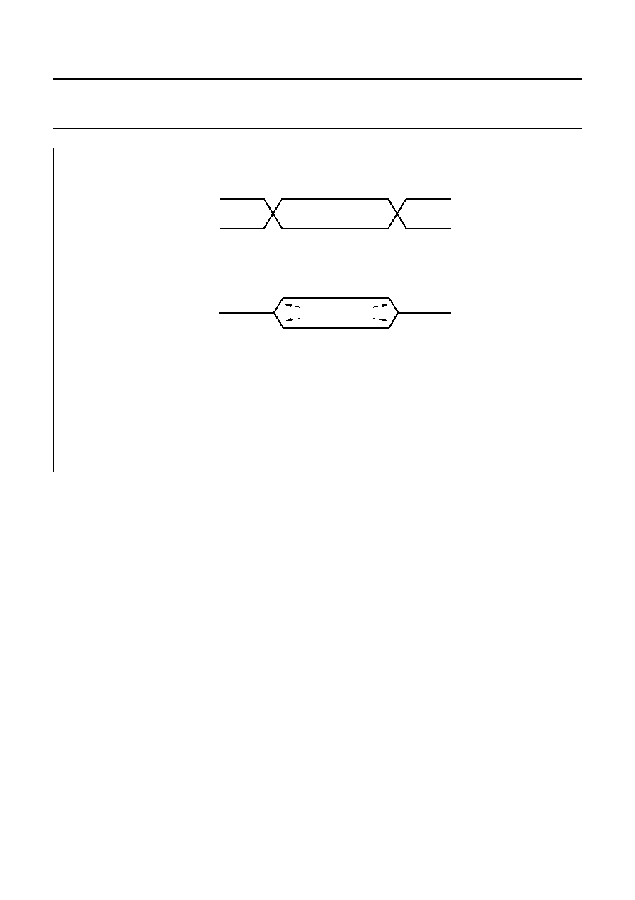
1998 Apr 07
55
Philips Semiconductors
Product specification
8-bit Flash microcontrollers
P89C738; P89C739
Fig.30 AC testing input.
handbook, full pagewidth
MGK209
0.2VDD
+
0.9
0.2VDD
-
0.1
VDD
-
0.5
0.45 V
handbook, full pagewidth
MGK210
timing
reference points
VLOAD
+
0.1 V
VLOAD
-
0.1 V
VOH
-
0.1 V
VOL
+
0.1 V
VLOAD
a. Output waveform.
b. Float waveform
AC testing inputs are driven at 2.4 V for a logic 1 and 0.45 V for a logic 0.
Timing measurements are taken at 2.0 V for a logic 1 and 0.8 V for a logic 0, see Fig.30a.
The float state is defined as the point at which a Port 0 pin sinks 3.2 mA or sources 400
µ
A at
the voltage test levels, see Fig.30b.

1998 Apr 07
56
Philips Semiconductors
Product specification
8-bit Flash microcontrollers
P89C738; P89C739
Fig.31 Instruction cycle timing.
handbook, full pagewidth
MGA180
P1 P2
S1
P1 P2
S2
P1 P2
S3
P1 P2
S4
P1 P2
S5
P1 P2
S6
P1 P2
S1
P1 P2
S2
P1 P2
S3
P1 P2
S4
P1 P2
S5
P1 P2
S6
one machine cycle
one machine cycle
XTAL1
INPUT
address
A0 - A7
inst.
in
address
A0 - A7
inst.
in
address
A0 - A7
inst.
in
address
A0 - A7
inst.
in
address A8 - A15
address A8 - A15
address A8 - A15
address A8 - A15
address
A0 - A7
inst.
in
address
A0 - A7
inst.
in
address
A0 - A7
data output or data input
address A8 - A15
address A8 - A15 or Port 2 out
address A8 - A15
old data
new data
sampling time of I/O port pins during input (including INT0 and INT1)
SERIAL
PORT
CLOCK
PORT
INPUT
PORT
OUTPUT
PORT 2
BUS
(PORT 0)
read or
write of
external data
memory
PORT 2
BUS
(PORT 0)
external
program
memory
fetch
WR
RD
only active
during a write
to external
data memory
only active
during a read
from external
data memory
PSEN
ALE
dotted lines
are valid when
RD or WR are
active

1998 Apr 07
57
Philips Semiconductors
Product specification
8-bit Flash microcontrollers
P89C738; P89C739
21.1
Serial Port characteristics
Table 36 Serial Port timing: Shift Register mode
V
DD
= 5 V
±
10%; V
SS
= 0 V; T
amb
= 0 to 70
∞
C; load capacitance = 80 pF.
SYMBOL
PARAMETER
12 MHz
OSCILLATOR
VARIABLE OSCILLATOR
UNIT
MIN.
MAX.
MIN.
MAX.
t
XLXL
Serial Port clock cycle time
1
-
12t
clk
-
µ
s
t
QVXH
output data set-up to clock rising edge
700
-
10t
clk
-
133
-
ns
t
XHQX
output data hold after clock rising edge 50
-
2t
clk
-
117
-
ns
t
XHDX
input data hold after clock rising edge
0
-
0
-
ns
t
XHDV
clock rising edge to input data valid
-
700
-
10t
clk
-
133
ns
Fig.32 Shift register mode timing.
handbook, full pagewidth
VALID
VALID
VALID
VALID
VALID
VALID
VALID
VALID
INSTRUCTION
ALE
8
7
6
5
4
3
2
1
0
CLOCK
WRITE TO SBUF
OUTPUT DATA
CLEAR RI
INPUT DATA
t XLXL
t XHQX
t QVXH
tXHDV
tXHDX
SET RI
SET TI
MGA179

1998 Apr 07
58
Philips Semiconductors
Product specification
8-bit Flash microcontrollers
P89C738; P89C739
21.2
Timing waveforms
Fig.33 External program memory read cycle.
handbook, full pagewidth
MGK206
ALE
PORT 0
PORT 2
tLLAX
tLLPL
tLHLL
tPLPH
tAVLL
A8 to A15
A0 to A15
A0 to A7
instr in
A0 to A7
PSEN
tAVIV
tLLIV
tPLIV
tPXIZ
tPLAZ
tPXIX
Fig.34 External data memory read cycle.
handbook, full pagewidth
MGK207
ALE
PORT 0
PORT 2
tLLAX
tAVLL
P2.0 to P2.7 or A8 to A15 from DPH
A0 to A15 from PCH
data in
A0 to A7
from RI or DPL
instr in
A0 to A7 from PCL
PSEN
tWHLH
tRLAZ
tLLDV
tAVWL
tAVDV
tLLWL
tRLRH
tRLDV
tRHDZ
tRHDX
RD

1998 Apr 07
59
Philips Semiconductors
Product specification
8-bit Flash microcontrollers
P89C738; P89C739
Fig.35 External data memory write cycle.
handbook, full pagewidth
MGK208
ALE
PORT 0
PORT 2
tLLAX
tAVLL
P2.0 to P2.7 or A8 to A15 from DPF
A0 to A15 from PCH
data output
A0 to A7
from RI or DPL
instr in
A0 to A7 from PCL
PSEN
tWHLH
tAVWL
tLLWL
tWLWH
tWHQX
tQVWX
WR
21.3
Timing symbol naming conventions
Each timing symbol has five characters. The first character
is always a `t' (= time). The remaining four characters of
the symbol (typed in subscript), depending on their relative
positions, indicate the name of a signal or the logical status
of that signal. The designations are as follows:
∑
A = address
∑
C = clock
∑
D = input data
∑
H = logic level HIGH
∑
I = instruction (program memory contents)
∑
L = Logic level LOW or ALE
∑
P = PSEN
∑
Q = output data
∑
R = RD signal
∑
t = time
∑
V = valid
∑
W = WR signal
∑
X = no longer a valid logic level
∑
Z = float.
Examples:
t
AVLL
= time for address valid to ALE LOW
t
LLPL
= time for ALE LOW to PSEN LOW.

1998 Apr 07
60
Philips Semiconductors
Product specification
8-bit Flash microcontrollers
P89C738; P89C739
22 PACKAGE OUTLINES
UNIT
A
max.
1
2
b
1
c
D
E
e
M
H
L
REFERENCES
OUTLINE
VERSION
EUROPEAN
PROJECTION
ISSUE DATE
IEC
JEDEC
EIAJ
mm
inches
DIMENSIONS (inch dimensions are derived from the original mm dimensions)
SOT129-1
92-11-17
95-01-14
A
min.
A
max.
b
Z
max.
w
M
E
e
1
1.70
1.14
0.53
0.38
0.36
0.23
52.50
51.50
14.1
13.7
3.60
3.05
0.254
2.54
15.24
15.80
15.24
17.42
15.90
2.25
4.7
0.51
4.0
0.067
0.045
0.021
0.015
0.014
0.009
2.067
2.028
0.56
0.54
0.14
0.12
0.01
0.10
0.60
0.62
0.60
0.69
0.63
0.089
0.19
0.020
0.16
051G08
MO-015AJ
M
H
c
(e )
1
M
E
A
L
seating plane
A
1
w
M
b
1
e
D
A
2
Z
40
1
21
20
b
E
pin 1 index
0
5
10 mm
scale
Note
1. Plastic or metal protrusions of 0.25 mm maximum per side are not included.
(1)
(1)
(1)
DIP40: plastic dual in-line package; 40 leads (600 mil)
SOT129-1

1998 Apr 07
61
Philips Semiconductors
Product specification
8-bit Flash microcontrollers
P89C738; P89C739
UNIT
A
1
A
2
A
3
b
p
c
E
(1)
e
H
E
L
L
p
Z
y
w
v
REFERENCES
OUTLINE
VERSION
EUROPEAN
PROJECTION
ISSUE DATE
IEC
JEDEC
EIAJ
mm
0.36
0.10
2.87
2.57
0.25
0.50
0.35
0.25
0.13
14.1
13.9
1
18.2
17.6
1.2
0.8
7
0
o
o
0.2
0.1
0.2
1.95
DIMENSIONS (mm are the original dimensions)
Note
1. Plastic or metal protrusions of 0.25 mm maximum per side are not included.
1.0
0.6
SOT319-1
95-02-04
97-08-01
D
(1)
(1)
(1)
20.1
19.9
H
D
24.2
23.6
E
Z
1.2
0.8
D
b
p
e
E
A
1
A
L
p
detail X
L
(A )
3
B
19
y
c
D
H
b
p
E
H
A
2
v
M
B
D
Z D
A
Z E
e
v
M
A
w
M
1
64
52
51
33
32
20
X
w
M
0
5
10 mm
scale
pin 1 index
64 leads (lead length 1.95 mm); body 14 x 20 x 2.7 mm; high stand-off height
QFP64: plastic quad flat package;
SOT319-1
A
max.
3.3

1998 Apr 07
62
Philips Semiconductors
Product specification
8-bit Flash microcontrollers
P89C738; P89C739
23 SOLDERING
23.1
Introduction
There is no soldering method that is ideal for all IC
packages. Wave soldering is often preferred when
through-hole and surface mounted components are mixed
on one printed-circuit board. However, wave soldering is
not always suitable for surface mounted ICs, or for
printed-circuits with high population densities. In these
situations reflow soldering is often used.
This text gives a very brief insight to a complex technology.
A more in-depth account of soldering ICs can be found in
our
"Data Handbook IC26; Integrated Circuit Packages"
(order code 9398 652 90011).
23.2
DIP
23.2.1
S
OLDERING BY DIPPING OR BY WAVE
The maximum permissible temperature of the solder is
260
∞
C; solder at this temperature must not be in contact
with the joint for more than 5 seconds. The total contact
time of successive solder waves must not exceed
5 seconds.
The device may be mounted up to the seating plane, but
the temperature of the plastic body must not exceed the
specified maximum storage temperature (T
stg max
). If the
printed-circuit board has been pre-heated, forced cooling
may be necessary immediately after soldering to keep the
temperature within the permissible limit.
23.2.2
R
EPAIRING SOLDERED JOINTS
Apply a low voltage soldering iron (less than 24 V) to the
lead(s) of the package, below the seating plane or not
more than 2 mm above it. If the temperature of the
soldering iron bit is less than 300
∞
C it may remain in
contact for up to 10 seconds. If the bit temperature is
between 300 and 400
∞
C, contact may be up to 5 seconds.
23.3
PLCC and QFP
23.3.1
R
EFLOW SOLDERING
Reflow soldering techniques are suitable for all PLCC and
QFP packages.
The choice of heating method may be influenced by larger
plastic PLCC and QFP packages (44 leads, or more).
If infrared or vapour phase heating is used and the large
packages are not absolutely dry (less than 0.1% moisture
content by weight), vaporization of the small amount of
moisture in them can cause cracking of the plastic body.
For details, refer to the Drypack information in the
"Data Handbook IC26; Integrated Circuit Packages;
Section: Packing Methods".
Reflow soldering requires solder paste (a suspension of
fine solder particles, flux and binding agent) to be applied
to the printed-circuit board by screen printing, stencilling or
pressure-syringe dispensing before package placement.
Several methods exist for reflowing; for example,
infrared/convection heating in a conveyor type oven.
Throughput times (preheating, soldering and cooling) vary
between 50 and 300 seconds depending on heating
method. Typical reflow peak temperatures range from
215 to 250
∞
C.
23.3.2
W
AVE SOLDERING
23.3.2.1
PLCC
Wave soldering techniques can be used for all PLCC
packages if the following conditions are observed:
∑
A double-wave (a turbulent wave with high upward
pressure followed by a smooth laminar wave) soldering
technique should be used.
∑
The longitudinal axis of the package footprint must be
parallel to the solder flow.
∑
The package footprint must incorporate solder thieves at
the downstream corners.
23.3.2.2
QFP
Wave soldering is not recommended for QFP packages.
This is because of the likelihood of solder bridging due to
closely-spaced leads and the possibility of incomplete
solder penetration in multi-lead devices.
If wave soldering cannot be avoided, for QFP
packages with a pitch (e) larger than 0.5 mm, the
following conditions must be observed:
∑
A double-wave (a turbulent wave with high upward
pressure followed by a smooth laminar wave)
soldering technique should be used.
∑
The footprint must be at an angle of 45
∞
to the board
direction and must incorporate solder thieves
downstream and at the side corners.
CAUTION
Wave soldering is NOT applicable for all QFP
packages with a pitch (e) equal or less than 0.5 mm.
1998 Apr 07
63
Philips Semiconductors
Product specification
8-bit Flash microcontrollers
P89C738; P89C739
23.3.2.3
Method (PLCC and QFP)
During placement and before soldering, the package must
be fixed with a droplet of adhesive. The adhesive can be
applied by screen printing, pin transfer or syringe
dispensing. The package can be soldered after the
adhesive is cured.
Maximum permissible solder temperature is 260
∞
C, and
maximum duration of package immersion in solder is
10 seconds, if cooled to less than 150
∞
C within
6 seconds. Typical dwell time is 4 seconds at 250
∞
C.
A mildly-activated flux will eliminate the need for removal
of corrosive residues in most applications.
23.3.3
R
EPAIRING SOLDERED JOINTS
Fix the component by first soldering two diagonally-
opposite end leads. Use only a low voltage soldering iron
(less than 24 V) applied to the flat part of the lead. Contact
time must be limited to 10 seconds at up to 300
∞
C. When
using a dedicated tool, all other leads can be soldered in
one operation within 2 to 5 seconds between
270 and 320
∞
C.
24 DEFINITIONS
25 LIFE SUPPORT APPLICATIONS
These products are not designed for use in life support appliances, devices, or systems where malfunction of these
products can reasonably be expected to result in personal injury. Philips customers using or selling these products for
use in such applications do so at their own risk and agree to fully indemnify Philips for any damages resulting from such
improper use or sale.
Data sheet status
Objective specification
This data sheet contains target or goal specifications for product development.
Preliminary specification
This data sheet contains preliminary data; supplementary data may be published later.
Product specification
This data sheet contains final product specifications.
Limiting values
Limiting values given are in accordance with the Absolute Maximum Rating System (IEC 134). Stress above one or
more of the limiting values may cause permanent damage to the device. These are stress ratings only and operation
of the device at these or at any other conditions above those given in the Characteristics sections of the specification
is not implied. Exposure to limiting values for extended periods may affect device reliability.
Application information
Where application information is given, it is advisory and does not form part of the specification.

Internet: http://www.semiconductors.philips.com
Philips Semiconductors ≠ a worldwide company
© Philips Electronics N.V. 1998
SCA59
All rights are reserved. Reproduction in whole or in part is prohibited without the prior written consent of the copyright owner.
The information presented in this document does not form part of any quotation or contract, is believed to be accurate and reliable and may be changed
without notice. No liability will be accepted by the publisher for any consequence of its use. Publication thereof does not convey nor imply any license
under patent- or other industrial or intellectual property rights.
Middle East: see Italy
Netherlands: Postbus 90050, 5600 PB EINDHOVEN, Bldg. VB,
Tel. +31 40 27 82785, Fax. +31 40 27 88399
New Zealand: 2 Wagener Place, C.P.O. Box 1041, AUCKLAND,
Tel. +64 9 849 4160, Fax. +64 9 849 7811
Norway: Box 1, Manglerud 0612, OSLO,
Tel. +47 22 74 8000, Fax. +47 22 74 8341
Pakistan: see Singapore
Philippines: Philips Semiconductors Philippines Inc.,
106 Valero St. Salcedo Village, P.O. Box 2108 MCC, MAKATI,
Metro MANILA, Tel. +63 2 816 6380, Fax. +63 2 817 3474
Poland: Ul. Lukiska 10, PL 04-123 WARSZAWA,
Tel. +48 22 612 2831, Fax. +48 22 612 2327
Portugal: see Spain
Romania: see Italy
Russia: Philips Russia, Ul. Usatcheva 35A, 119048 MOSCOW,
Tel. +7 095 755 6918, Fax. +7 095 755 6919
Singapore: Lorong 1, Toa Payoh, SINGAPORE 319762,
Tel. +65 350 2538, Fax. +65 251 6500
Slovakia: see Austria
Slovenia: see Italy
South Africa: S.A. PHILIPS Pty Ltd., 195-215 Main Road Martindale,
2092 JOHANNESBURG, P.O. Box 7430 Johannesburg 2000,
Tel. +27 11 470 5911, Fax. +27 11 470 5494
South America: Al. Vicente Pinzon, 173, 6th floor,
04547-130 S√O PAULO, SP, Brazil,
Tel. +55 11 821 2333, Fax. +55 11 821 2382
Spain: Balmes 22, 08007 BARCELONA,
Tel. +34 3 301 6312, Fax. +34 3 301 4107
Sweden: Kottbygatan 7, Akalla, S-16485 STOCKHOLM,
Tel. +46 8 5985 2000, Fax. +46 8 5985 2745
Switzerland: Allmendstrasse 140, CH-8027 ZÐRICH,
Tel. +41 1 488 2741 Fax. +41 1 488 3263
Taiwan: Philips Semiconductors, 6F, No. 96, Chien Kuo N. Rd., Sec. 1,
TAIPEI, Taiwan Tel. +886 2 2134 2865, Fax. +886 2 2134 2874
Thailand: PHILIPS ELECTRONICS (THAILAND) Ltd.,
209/2 Sanpavuth-Bangna Road Prakanong, BANGKOK 10260,
Tel. +66 2 745 4090, Fax. +66 2 398 0793
Turkey: Talatpasa Cad. No. 5, 80640 GÐLTEPE/ISTANBUL,
Tel. +90 212 279 2770, Fax. +90 212 282 6707
Ukraine: PHILIPS UKRAINE, 4 Patrice Lumumba str., Building B, Floor 7,
252042 KIEV, Tel. +380 44 264 2776, Fax. +380 44 268 0461
United Kingdom: Philips Semiconductors Ltd., 276 Bath Road, Hayes,
MIDDLESEX UB3 5BX, Tel. +44 181 730 5000, Fax. +44 181 754 8421
United States: 811 East Arques Avenue, SUNNYVALE, CA 94088-3409,
Tel. +1 800 234 7381
Uruguay: see South America
Vietnam: see Singapore
Yugoslavia: PHILIPS, Trg N. Pasica 5/v, 11000 BEOGRAD,
Tel. +381 11 625 344, Fax.+381 11 635 777
For all other countries apply to: Philips Semiconductors,
International Marketing & Sales Communications, Building BE-p, P.O. Box 218,
5600 MD EINDHOVEN, The Netherlands, Fax. +31 40 27 24825
Argentina: see South America
Australia: 34 Waterloo Road, NORTH RYDE, NSW 2113,
Tel. +61 2 9805 4455, Fax. +61 2 9805 4466
Austria: Computerstr. 6, A-1101 WIEN, P.O. Box 213, Tel. +43 160 1010,
Fax. +43 160 101 1210
Belarus: Hotel Minsk Business Center, Bld. 3, r. 1211, Volodarski Str. 6,
220050 MINSK, Tel. +375 172 200 733, Fax. +375 172 200 773
Belgium: see The Netherlands
Brazil: see South America
Bulgaria: Philips Bulgaria Ltd., Energoproject, 15th floor,
51 James Bourchier Blvd., 1407 SOFIA,
Tel. +359 2 689 211, Fax. +359 2 689 102
Canada: PHILIPS SEMICONDUCTORS/COMPONENTS,
Tel. +1 800 234 7381
China/Hong Kong: 501 Hong Kong Industrial Technology Centre,
72 Tat Chee Avenue, Kowloon Tong, HONG KONG,
Tel. +852 2319 7888, Fax. +852 2319 7700
Colombia: see South America
Czech Republic: see Austria
Denmark: Prags Boulevard 80, PB 1919, DK-2300 COPENHAGEN S,
Tel. +45 32 88 2636, Fax. +45 31 57 0044
Finland: Sinikalliontie 3, FIN-02630 ESPOO,
Tel. +358 9 615800, Fax. +358 9 61580920
France: 51 Rue Carnot, BP317, 92156 SURESNES Cedex,
Tel. +33 1 40 99 6161, Fax. +33 1 40 99 6427
Germany: Hammerbrookstraþe 69, D-20097 HAMBURG,
Tel. +49 40 23 53 60, Fax. +49 40 23 536 300
Greece: No. 15, 25th March Street, GR 17778 TAVROS/ATHENS,
Tel. +30 1 4894 339/239, Fax. +30 1 4814 240
Hungary: see Austria
India: Philips INDIA Ltd, Band Box Building, 2nd floor,
254-D, Dr. Annie Besant Road, Worli, MUMBAI 400 025,
Tel. +91 22 493 8541, Fax. +91 22 493 0966
Indonesia: PT Philips Development Corporation, Semiconductors Division,
Gedung Philips, Jl. Buncit Raya Kav.99-100, JAKARTA 12510,
Tel. +62 21 794 0040 ext. 2501, Fax. +62 21 794 0080
Ireland: Newstead, Clonskeagh, DUBLIN 14,
Tel. +353 1 7640 000, Fax. +353 1 7640 200
Israel: RAPAC Electronics, 7 Kehilat Saloniki St, PO Box 18053,
TEL AVIV 61180, Tel. +972 3 645 0444, Fax. +972 3 649 1007
Italy: PHILIPS SEMICONDUCTORS, Piazza IV Novembre 3,
20124 MILANO, Tel. +39 2 6752 2531, Fax. +39 2 6752 2557
Japan: Philips Bldg 13-37, Kohnan 2-chome, Minato-ku, TOKYO 108,
Tel. +81 3 3740 5130, Fax. +81 3 3740 5077
Korea: Philips House, 260-199 Itaewon-dong, Yongsan-ku, SEOUL,
Tel. +82 2 709 1412, Fax. +82 2 709 1415
Malaysia: No. 76 Jalan Universiti, 46200 PETALING JAYA, SELANGOR,
Tel. +60 3 750 5214, Fax. +60 3 757 4880
Mexico: 5900 Gateway East, Suite 200, EL PASO, TEXAS 79905,
Tel. +9-5 800 234 7381
Printed in The Netherlands
455104/1200/02/pp64
Date of release: 1998 Apr 07
Document order number:
9397 750 03529