 | –≠–ª–µ–∫—Ç—Ä–æ–Ω–Ω—ã–π –∫–æ–º–ø–æ–Ω–µ–Ω—Ç: PCA1463U | –°–∫–∞—á–∞—Ç—å:  PDF PDF  ZIP ZIP |

DATA SHEET
Product specification
Supersedes data of 1998 Mar 18
File under Integrated Circuits, IC16
1998 Apr 21
INTEGRATED CIRCUITS
PCA146x series
32 kHz watch circuits with adaptive
motor pulse

1998 Apr 21
2
Philips Semiconductors
Product specification
32 kHz watch circuits with adaptive motor
pulse
PCA146x series
FEATURES
∑
32 kHz oscillator, amplitude regulated with excellent
frequency stability
∑
High immunity of the oscillator to leakage currents
∑
Time calibration electrically programmable and
reprogrammable (via EEPROM)
∑
A quartz crystal is the only external component required
∑
Very low current consumption; typically 170 nA
∑
Output for bipolar stepping motors of different types
∑
Up to 50% reduction in motor current compared with
conventional circuits, by self adaption of the motor pulse
width to match the required torque of the motor
∑
No loss of motor steps possible because of on-chip
detection of the induced motor voltage
∑
Detector for lithium or silver-oxide battery voltage levels
∑
Indication for battery end-of-life
∑
Stop function for accurate timing
∑
Power-on reset for fast testing
∑
Various test modes for testing the mechanical parts of
the watch and the IC.
GENERAL DESCRIPTION
The PCA146x series devices are CMOS integrated circuits
specially suited for battery-operated,
quartz-crystal-controlled wrist-watches, with a bipolar
stepping motor.
ORDERING INFORMATION
Note
1. Figure 1 and Chapter "Package outline" show details of standard package, available for large orders only.
Chapter "Chip dimensions and bonding pad locations" shows exact pad locations for other delivery formats.
TYPE
NUMBER
PACKAGE
(1)
NAME
DESCRIPTION
VERSION
PCA1461U
-
chip in tray
-
PCA1461U/10
-
chip on foil
-
PCA1462U
-
chip in tray
-
PCA1462U/7
-
chip with bumps on tape
-
PCA1462U/10
-
chip on foil
-
PCA1463U
-
chip in tray
-
PCA1463U/10
-
chip on foil
-
PCA1465U/10
-
chip on foil
-
PCA1465U/7
-
chip with bumps on tape
-
PCA1467U/10
-
chip on foil
-

1998 Apr 21
3
Philips Semiconductors
Product specification
32 kHz watch circuits with adaptive motor
pulse
PCA146x series
PINNING
SYMBOL
PIN
DESCRIPTION
V
SS
1
ground (0 V)
TEST
2
test output
OSC IN
3
oscillator input
OSC OUT
4
oscillator output
V
DD
5
supply voltage
M1
6
motor 1 output
M2
7
motor 2 output
RESET
8
reset input
Fig.1 Pin configuration, PCA146xT, (PMFP8).
1
2
3
4
8
7
6
5
PCA146xT
VSS
TEST
OSC IN
OSC OUT
RESET
M2
M1
VDD
MSA937
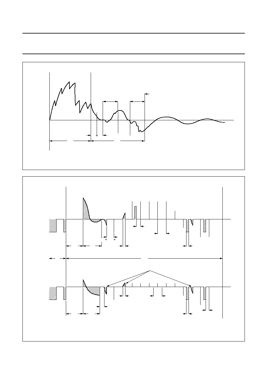
FUNCTIONAL DESCRIPTION AND TESTING
The motor output delivers pulses of six different stages
depending on the torque required to turn the motor
(Figs. 3 and 4). Every motor pulse is followed by a
detection phase which monitors the waveform of the
induced motor voltage. When a step is missed a correction
sequence will be started (Fig.2).
Motor pulses
The circuit produces motor pulses of six different stages
(stage 1 to 5, stage 8). Each stage has two independent
modes: silver-oxide and lithium. The voltage level of V
DD
determines which mode is selected (see Section "Voltage
level detector").
Stages 1 to 5 (both modes) are used in normal operation,
stage 8 occurs under the following conditions:
∑
Correction pulse after a missing step (both modes)
∑
End-of-life mode
∑
If stage 5 is not enough to turn the motor (both modes).
In the silver-oxide mode, the ON state of the motor pulse
varies between 56.25% and 100% of the duty factor
t
DF
= 977
µ
s depending on the stage (Fig.3). It increases
in steps of 6.25% per stage.
In the lithium mode, the ON state of the motor pulse is
reduced by 18.75% of the duty factor t
DF
(Fig.4) to
compensate for the increase in the voltage level.
After a RESET the circuit always starts and continues with
stage 1, when all motor pulses have been executed.
A failure to execute all motor pulses results in the circuit
going into stage 2, this sequence will be repeated through
to stage 8.
When the motor pulses at stage 5 are not large enough to
turn the motor, stage 8 is implemented for a maximum of
8 minutes with no attempt to keep current consumption
low. After stage 8 has been executed the procedure is
repeated from RESET.
The circuit operates for 8 minutes at a fixed stage, if every
motor pulse is executed. The next 480 motor pulses are
then produced at the next lower stage unless a missing
step is detected. If a step is missed a correction sequence
is produced and for a maximum of 8 minutes the motor
pulses are increased by one stage.
1998 Apr 21
4
Philips Semiconductors
Product specification
32 kHz watch circuits with adaptive motor
pulse
PCA146x series
Fig.2 Possible motor output waveform in normal operation with motor connected.
MSA942
MOTOR
PULSE
DETECTION
t P
t D
t C
POSSIBLE CORRECTION
SEQUENCE
t T
M1 - M2
V
1998
Apr
21
5
Philips Semiconductors
Product specification
32
kHz watch circuits with adaptive motor
pulse
PCA146x series
This text is here in white to force landscape pages to be rotated correctly when browsing through the pdf in the Acrobat reader.This text is here in
_
white to force landscape pages to be rotated correctly when browsing through the pdf in the Acrobat reader.This text is here inThis text is here in
white to force landscape pages to be rotated correctly when browsing through the pdf in the Acrobat reader. white to force landscape pages to be ...
MSA947
STAGE 1
STAGE 2
STAGE 3
STAGE 4
STAGE 5
STAGE 8
t = 3.9 ms
P3
t = 5.86 ms
P2
t = 7.81 ms
P1
56.25 %
62.50 %
68.75 %
75.00 %
81.25 %
100.00 %
t
t
DF
DF
SOFF
=
t
ONL
t
SOFF
t
DF
t = 977
µ
s
SON
t
t = 488
µ
s
SONF
ON
t
= SON
t
t DF
Fig.3 Motor pulses in the silver-oxide mode (V
DD
= 1.55 V).
t
OFF
for stage 1 to 5 = 488
µ
s
-
stage
◊
61
µ
s
t
ON
for stage 1 to 5 = 488
µ
s + stage
◊
61
µ
s
1998
Apr
21
6
Philips Semiconductors
Product specification
32
kHz watch circuits with adaptive motor
pulse
PCA146x series
This text is here in white to force landscape pages to be rotated correctly when browsing through the pdf in the Acrobat reader.This text is here in
_
white to force landscape pages to be rotated correctly when browsing through the pdf in the Acrobat reader.This text is here inThis text is here in
white to force landscape pages to be rotated correctly when browsing through the pdf in the Acrobat reader. white to force landscape pages to be ...
MSA946
STAGE 1
STAGE 2
STAGE 3
STAGE 4
STAGE 5
STAGE 8
t = 3.9 ms
P3
t = 5.86 ms
P2
t = 7.81 ms
P1
37.50 %
43.75 %
50.00 %
56.25 %
62.50 %
81.25 %
t DF LOFF
DF
t
LOFF
t
ON
t
=
t
ONL
t
AOFF
t
DF
t = 977
µ
s
LOFF
t
t = 183
µ
s
AOFF
t = 244
µ
s
LONF
Fig.4 Motor pulses in the lithium mode (V
DD
= 2.1 V).
t
OFF
for stage 1 to 5 = 672
µ
s
-
stage
◊
61
µ
s
t
ON
for stage 1 to 5 = 305
µ
s + stage
◊
61
µ
s
1998 Apr 21
7
Philips Semiconductors
Product specification
32 kHz watch circuits with adaptive motor
pulse
PCA146x series
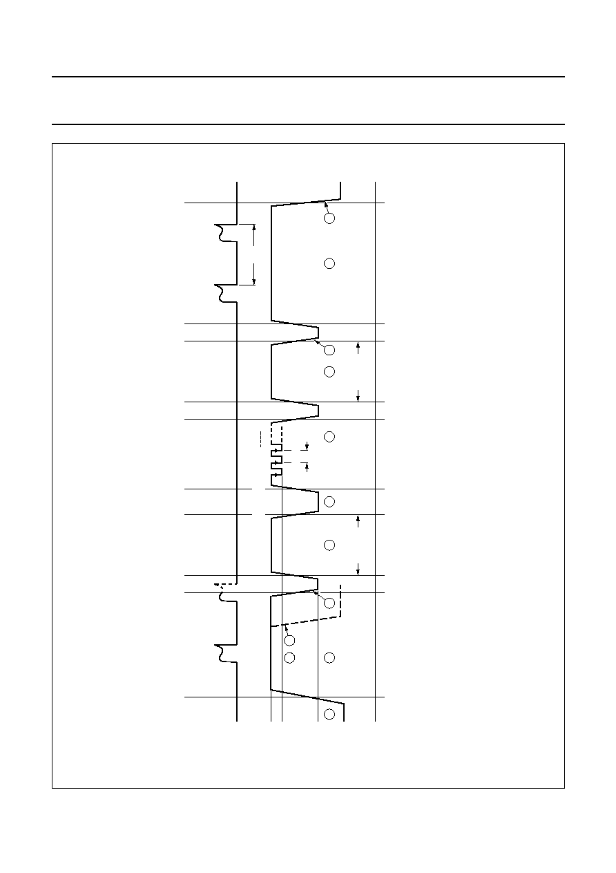
Voltage level detector
The supply voltage is compared with the internal voltage
reference V
LIT
and V
EOL
every minute. The first voltage
level detection is carried out 30 ms after RESET.
When a lithium voltage level is detected (V
DD
V
LIT
), the
circuit starts operating in the lithium mode (Fig.4).
When the detected V
DD
voltage level is between V
LIT
and
V
EOL
, the circuit operates in the silver-oxide mode (Fig.3).
If the battery end-of-life is detected (V
DD
< V
EOL
), the
detection and stage control is switched OFF and the
waveform produced is an unchopped version of the
stage 8 waveform. To indicate this condition the waveform
is produced in bursts of 4 pulses every 4 s.
Detection of motor movement
After a motor pulse, the motor is short-circuited to V
DD
for
1 ms. Afterwards the energy in the motor inductor will be
dissipated to measure only the current generated by the
induced motor voltage. During the time t
DI
(dissipation of
energy time) all switches shown in Fig.5 are open to
reduce the current as fast as possible. The current will now
flow through the diodes D3 and D2, or D4 and D1. Then
the first of 52 possible measurement cycles (t
MC
) starts to
measure the induced current.
Fig.5 Motor driving and detecting circuit.
MSA941
VDD
VSS
MOTOR
M1
M2
N1
D3
P1
D1
L1
L2
N2
D4
P2
D2

1998 Apr 21
8
Philips Semiconductors
Product specification
32 kHz watch circuits with adaptive motor
pulse
PCA146x series
Detection criteria
The PCA146x uses current detection in two defined parts
of the detection phase to determine if the motor has moved
(refer to Figs 6 and 7). The detection criteria are:
part 1
∑
Minimum value of P = 1; where P = number of
measured positive current polarities after t
DI
.
part 2
∑
Minimum value of N = 2; where N = number of
measured positive current polarities since the first
negative current polarity after part 1 was detected
(see Fig.6).
If the opposite polarity is measured in one part, the internal
counter is reset, so the results of all measurements in this
part are ignored.
The waveform of the induced current must enable all these
measurements within the time t
D
after the end of a positive
motor pulse in order to be accepted as a waveform of an
executed motor pulse.
If the detection criterion is satisfied earlier, a measurement
cycle will not be started and the switches P1 and P2 stay
closed, the motor is switched to V
DD
.
Every measurement cycle (t
MC
) has 4 phases. These are
detailed in Table 1.
Note that detection and pulse width control will be switched
OFF when the battery voltage is below the end-of-life
voltage (V
EOL
), or if stage 5 is not sufficient to turn the
motor.
Table 1
Measurement cycle
SYMBOL
PHASE
DESCRIPTION
t
M1
1
During t
M1
the switches P1 and P2 are closed in order to switch the motor to V
DD
, so the
induced current flows unaffected through the motor inductance.
t
M2
2
Measures the induced current; during a maximum time t
M2
all switches are open until a change
is sensed by one of the level detectors (L1, L2). The motor is short-circuited to V
DD
.
Depending on the direction of the interrupted current:
∑
The current flows through diodes D3 and D2, causing the voltage at M1 to decrease in relation
to M2;
∑
The current flows through diodes D4 and D1, causing the voltage at M2 to decrease in relation
to M1.
A successfully detected current polarity is normally characterized by a short pulse of
0.5 to 10
µ
s with a voltage up to
±
2.1 V, failed polarity detection by the maximum pulse width of
61
µ
s and a voltage of
±
0.5 V (see Fig.7).
t
M3
3
The switches P1 and P2 remain closed for the time t
M3
.
t
M4
4
If the circuit detects fewer pulses than P and N respectively, a pulse of the time t
M4
occurs to
reduce the induced current. Therefore P2 and P1 are opened and N1 and N2 are closed.
Otherwise P1 and P2 remain closed.
1998 Apr 21
9
Philips Semiconductors
Product specification
32 kHz watch circuits with adaptive motor
pulse
PCA146x series
Fig.6 Typical current waveform of a successfully executed motor pulse.
MSA944
MOTOR PULSE
DETECTION PHASE
I M1 - M2
part 1
part 2
detection criterion
is satisfied
t
t DS
t DI
t P
t D
Fig.7 Detection phase of the current waveform in Fig.6.
MSA945
MOTOR
PULSE
DETECTION PHASE
M1 - M2
V
t DS
t DI
t M3 t M4 t M1
t = 61
µ
s
M2
t = 244
µ
s
M1
t = 488
µ
s
MC
t = 61
µ
s
M2
t D
t P
M1
V
t DS
t DI
t = 61
µ
s
M2
t = 244
µ
s
M1
t = 488
µ
s
MC
t = 61
µ
s
M2
t = 244
µ
s
M1
detection
criterion is
satisfied
current polarity
not measured
1998 Apr 21
10
Philips Semiconductors
Product specification
32 kHz watch circuits with adaptive motor
pulse
PCA146x series
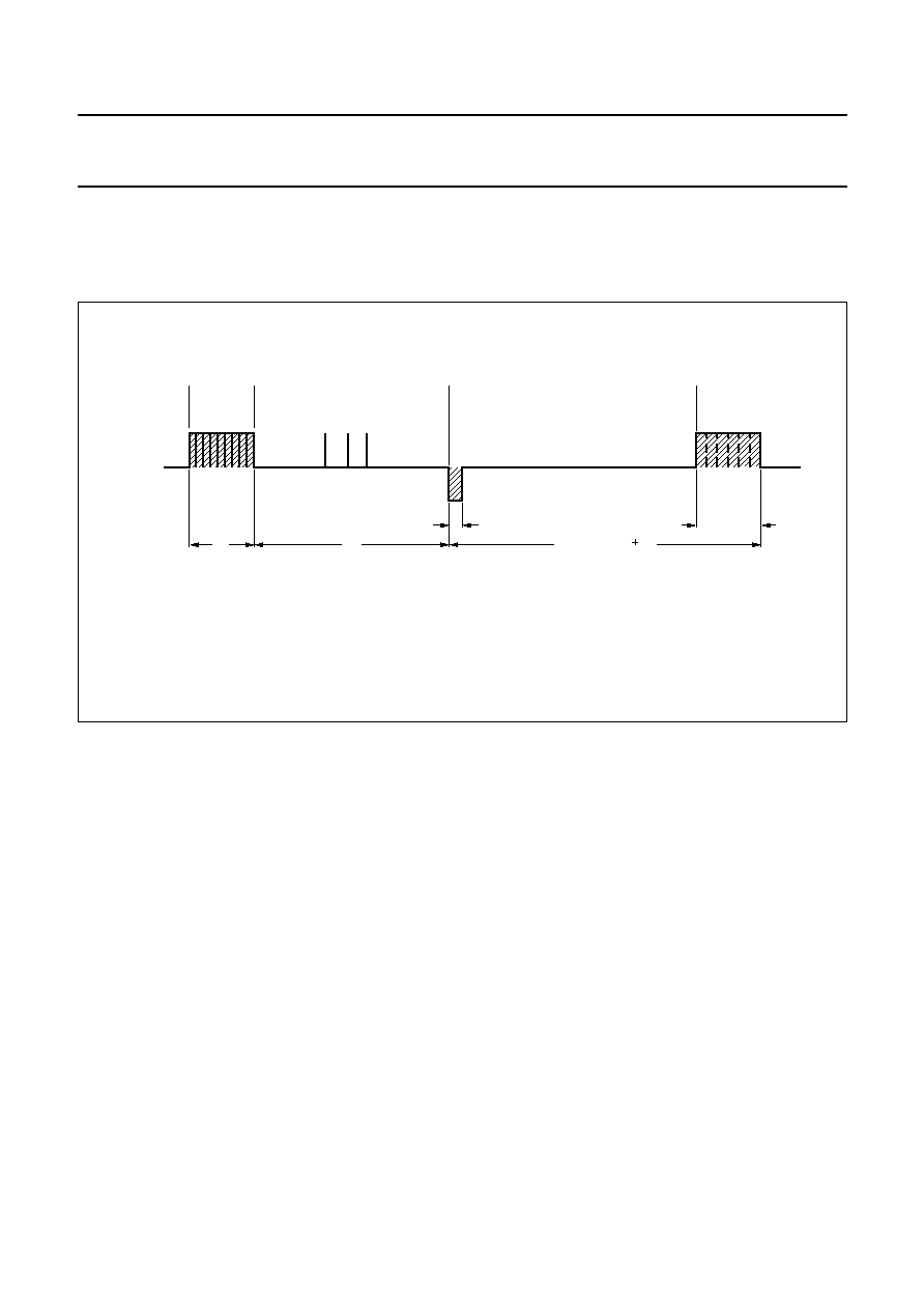
Correction sequence (see Fig.8)
If a missing step is detected, a correction sequence is produced. This consists of a small pulse (t
C1
) which gives the motor
a defined position and after 29.30 ms a pulse of stage 8 (t
C2
) to turn the motor.
Fig.8 Correction sequence after a missing motor step with motor connected.
MSA943
MOTOR
PULSE
DETECTION
CORRECTION SEQUENCE
t P
t C1
t D
M1 - M2
V
= 977
µ
s
t C = 30.27 ms t P
t C2 = t P
1998 Apr 21
11
Philips Semiconductors
Product specification
32 kHz watch circuits with adaptive motor
pulse
PCA146x series
Time calibration
Taking a normal quartz crystal with frequency 32768kHz,
frequency deviation (
f/f) of
±
15
◊
10
-
6
and C
L
= 8.2 pF;
the oscillator frequency is offset (by using non-symmetrical
internal oscillator input and output capacitances of 10 pF
and 15 pF) such that the frequency deviation is
positive-only. This positive deviation can then be
compensated for to maintain time-keeping accuracy.
Once the positive frequency deviation is measured, a
corresponding number `n' (see Table 2) can be
programmed into the device's EEPROM. This causes n
pulses of frequency 8192 Hz to be inhibited every minute
of operation, which achieves the required calibration.
The programming circuit is shown in Fig.9. The required
number n is programmed into EEPROM by varying V
DD
according to the steps shown in Fig.10, which are
explained below:
1. The positive quartz frequency deviation (
f/f) is
measured, and the corresponding values of n are
found according to Table 2.
2. V
DD
is increased to 5.1 V allowing the contents of the
EEPROM to be checked from the motor pulse period
t
T3
at nominal frequency.
3. V
DD
is decreased to 2.5 V during a motor pulse to
initialize a storing sequence.
4. The first V
DD
pulse to 5.1 V erases the contents of
EEPROM.
5. When the EEPROM is erased a logic 1 is at the TEST
pin.
6. V
DD
is increased to 5.1 V to read the data by pulsing
V
DD
n times to 4.5 V. After the n edge, V
DD
is
decreased to 2.5 V.
7. V
DD
is increased to 5.1 V to store n bits in the
EEPROM.
8. V
DD
is decreased to 2.5 V to terminate the storing
sequence and to return to operating mode.
9. V
DD
is increased to 5.1 V to check writing from the
motor pulse period t
T3
.
10. V
DD
is decreased to the operation voltage between
two motor pulses to return to operating mode.
(Decreasing V
DD
during the motor pulse would restart
the programming mode).
The time calibration can be reprogrammed up to 100
times.
Table 2
Quartz crystal frequency deviation, n and t
T3
Notes
1. Increments of 2.03
◊
10
-
6
/step.
2. Increments of 122
µ
s/step.
FREQUENCY
DEVIATION
f/f
(
◊
10
-
6
)
NUMBER OF
PULSES
(n)
t
T3
(ms)
0
(1)
0
31.250
(2)
+2.03
1
31.372
+4.06
2
31.494
.
.
.
.
.
.
.
.
.
+127.89
63
38.936
Fig.9 Circuit for programming the time calibration.
MSA940
VDD
M1
M2
RESET
VSS
TEST
OSC IN
OSC OUT
M
PCA146x
SERIES
1
2
3
4
8
7
6
5
32 kHz
SIGNAL GENERATOR
1998
Apr
21
12
Philips Semiconductors
Product specification
32
kHz watch circuits with adaptive motor
pulse
PCA146x series
This text is here in white to force landscape pages to be rotated correctly when browsing through the pdf in the Acrobat reader.This text is here in
_
white to force landscape pages to be rotated correctly when browsing through the pdf in the Acrobat reader.This text is here inThis text is here in
white to force landscape pages to be rotated correctly when browsing through the pdf in the Acrobat reader. white to force landscape pages to be ...
MSA948
V DDP
1
2
3
n
t = 1
µ
s
edge
0.1 ms
min.
t T3
CHECKING
STORING
DATA INPUT
ERASURE
CONTENT CHECKING
1
2
9
10
3
4
5
6
7
8
9
10
IDD
V (V)
DD
0 (V )
SS
2.5
1.5
4.5
5.1
(1)
(1)
(1)
(1)
t = 5 ms
E
t = 5 ms
S
(1) Rise and fall time should be greater than 400
µ
s/V for immediately correct checking.
Fig.10 V
DD
for programming.

1998 Apr 21
13
Philips Semiconductors
Product specification
32 kHz watch circuits with adaptive motor
pulse
PCA146x series
Power-on reset
For correct operation of the Power-on reset the rise time of
V
DD
from 0 V to 2.1 V should be less than 0.1 ms.
All resetable flip-flops are reset. Additionally the polarity of
the first motor pulse is positive: V
M1
-
V
M2
0 V.
Customer testing
An output frequency of 32 Hz is provided at RESET (pin 8)
to be used for exact frequency measurement. Every
minute a jitter occurs as a result of the inhibition, which
occurs 90 to 150 ms after disconnecting the RESET from
V
DD
.
Connecting the RESET to V
DD
stops the motor pulses
leaving them in a 3-state mode and sets the motor pulse
width for the next available motor pulse to stage 1 in the
silver-oxide mode. A 32 Hz signal without jitter is produced
at the TEST pin.
Debounce time RESET = 14.7 to 123.2 ms.
Connecting RESET to V
SS
activates Tests 1 and 2 and
disables the inhibition.
Test 1, V
DD
> V
EOL
. Normal function takes place except
that the motor pulse period is t
T1
= 125 ms instead of t
T
,
and the motor pulse stage is reduced every second
instead of every 8 minutes. At TEST a speeded-up
8 minute signal is available.
Test 2, V
DD
< V
EOL
. Motor pulses of stage 8 are produced,
with a time period of t
T2
= 31.25 ms.
Test and reset modes are terminated by disconnecting the
RESET pin.
Test 3, V
DD
> 5.1 V. Motor pulses of stage 8 are
produced, with a time period of t
T3
= 31.25 ms and
n
◊
122
µ
s to check the contents of the EEPROM. At
TEST a speeded-up cycle for motor pulse period signal t
T
is available at 1024 times its normal frequency.
Decreasing V
DD
voltage level to lower than 2.5 V between
two motor pulses returns the circuit to normal operating
conditions.
AVAILABLE TYPES
Refer to Chapters "Ordering information" and "Functional description and testing".
Note
1. U = Chip in tray; U/7 = chip with bumps on tape; U/10 = chip on foil.
SHORT
TYPE
NUMBER
DELIVERY
FORMAT
(1)
PERIOD
t
T
(s)
SPECIFICATIONS
PULSE
WIDTH
t
P
(ms)
DRIVE
(%)
DETECTION
CRITERION
EEPROM
BATTERY
EOL
DETECTION
REMARKS
1461
U; U/10
1
7.8
max. 100
81
P = 1
N = 2
yes
yes
1.5 V and
2.1 V Lithium
1462
U; U/7;
U/10
1
5.8
max. 100
81
P = 1
N = 2
yes
yes
1.5 V and
2.1 V Lithium
1463
U; U/10
1
3.9
max. 100
81
P = 1
N = 2
yes
yes
1.5 V and
2.1 V Lithium
1465
U/10; U/7
1
5.8
max. 100
P = 1
N = 2
yes
no
1.5 V
1467
U/10
1
7.8
max. 100
P = 1
N = 2
yes
no
1.5 V

1998 Apr 21
14
Philips Semiconductors
Product specification
32 kHz watch circuits with adaptive motor
pulse
PCA146x series
LIMITING VALUES
In accordance with the Absolute Maximum Rating System (IEC 134).
Note
1. Connecting the battery with reversed polarity does not destroy the circuit, but in this condition a large current flows,
which will rapidly discharge the battery.
HANDLING
Inputs and outputs are protected against electrostatic discharges in normal handling. However, to be totally safe, it is
advisable to take handling precautions appropriate to handling MOS devices. Advice can be found in
"Data Handbook IC16, General, Handling MOS Devices".
CHARACTERISTICS
V
DD
= 1.55 V; V
SS
= 0 V; f
osc
= 32.768 kHz; T
amb
= 25
∞
C; crystal: R
S
= 20 k
; C
1
= 2 to 3 fF; C
L
= 8 to 10 pF;
C
0
= 1 to 3 pF; unless otherwise specified.
Immunity against parasitic impedance = 20 M
between adjacent pins.
SYMBOL
PARAMETER
CONDITIONS
MIN.
MAX.
UNIT
V
DD
supply voltage
V
SS
= 0 V; note 1
-
1.8
+6
V
V
I
all input voltages
V
SS
V
DD
V
output short-circuit duration
indefinite
T
amb
operating ambient temperature
-
10
+60
∞
C
T
stg
storage temperature
-
30
+100
∞
C
SYMBOL
PARAMETER
CONDITIONS
MIN.
TYP.
MAX.
UNIT
Supply
V
DD1
supply voltage
T
amb
=
-
10 to +60
∞
C
1.2
1.55
2.5
V
V
DD
supply voltage variation
transient within 1.2 V and 2.5 V
-
-
0.25
V
V
DD2
supply voltage
programming
5.0
5.1
5.2
V
V
DDP
supply voltage pulse
variation
programming
0.55
0.6
0.65
V
I
DD1
supply current
between motor pulses
-
170
260
nA
I
DD2
supply current
V
DD
= 2.1 V
-
190
300
nA
I
DD3
supply current
stop mode; pin 8 connected to
V
DD
-
180
280
nA
I
DD4
supply current
V
DD
= 2.1 V
-
220
360
nA
I
DD5
supply current
T
amb
=
-
10 to +60
∞
C
-
-
600
nA
Motor output
V
sat
saturation voltage
(P + N)
R
M
= 2 k
; T
amb
=
-
10 to +60
∞
C
-
150
200
mV
Z
o(sc)
output short-circuit
impedance
between motor pulses
I
transistor
< 1 mA
-
200
300

1998 Apr 21
15
Philips Semiconductors
Product specification
32 kHz watch circuits with adaptive motor
pulse
PCA146x series
Note
1. Duty factor is 1 : 32 and RESET = V
DD
or V
SS
.
Oscillator
V
OSC ST
starting voltage
1.2
-
-
V
g
m
transconductance
V
i(p-p)
50 mV
6
15
-
µ
S
t
osc
start-up time
-
1
-
s
f/f
frequency stability
V
DD
= 100 mV
-
0.05
◊
10
-
6
0.3
◊
10
-
6
C
i
input capacitance
8
10
12
pF
C
o
output capacitance
12
15
18
pF
Voltage level detector
V
LIT
threshold voltage
1.62
1.80
1.98
V
V
EOL
threshold voltage
1.30
1.38
1.46
V
V
EOL
hysteresis of threshold
-
10
-
mV
TC
EOL
temperature coefficient
-
-
1
-
mV/K
Reset input
f
o
output frequency
-
32
-
Hz
V
o
output voltage swing
R = 1 M
; C = 10 pF
1.4
-
-
V
t
edge
edge time
R = 1 M
; C = 10 pF
-
1
-
µ
s
I
im
peak input current
note 1
-
320
-
nA
I
i(av)
average input current
-
10
-
nA
SYMBOL
PARAMETER
CONDITIONS
MIN.
TYP.
MAX.
UNIT

1998 Apr 21
16
Philips Semiconductors
Product specification
32 kHz watch circuits with adaptive motor
pulse
PCA146x series
TIMING PARAMETERS
Note
1. No option available when EOL indication is required.
SYMBOL
PARAMETER
SECTION
VALUE
OPTION
UNIT
t
T
cycle for motor pulse (note 1)
motor pulse (Figs 2, 3 and 4)
1
5, 10, 12 or 20 s
t
P
motor pulse width
7.81
3.9 or 5.9
ms
t
DF
duty factor
977
-
µ
s
t
ONL
last duty factor on
61 to 305
-
µ
s
t
v
voltage detection cycle
level mode
60
-
s
t
SON
duty factor on
silver-oxide mode (Fig.3)
550 to 794
-
µ
s
t
SOFF
duty factor off
427 to 183
-
µ
s
t
SONF
first duty factor on
488
-
µ
s
t
AOFF
additional duty factor off
lithium mode (Fig.4)
183
-
µ
s
t
LON
duty factor on
305 to 611
-
µ
s
t
LOFF
duty factor off
672 to 366
-
µ
s
t
LONF
first duty factor on
244
-
µ
s
t
E
EOL sequence
end-of-life mode
4
-
s
t
E1
motor pulse width
t
P
-
ms
t
E2
time between pulses
31.25
-
ms
t
D
detection sequence
detection (Fig.7)
4.3 to 28.3
-
ms
t
DS
short-circuited motor
977
-
µ
s
t
DI
dissipation of energy
977
-
µ
s
t
MC
measurement cycle
488
-
µ
s
t
M1
phase 1
244
-
µ
s
t
M2
phase 2 (measure window)
61
-
µ
s
t
M3
phase 3
122
-
µ
s
t
M4
phase 4
61
-
µ
s
P
positive current polarities
1
P < N
N
negative current polarities
2
2 to 6
t
C
correction sequence
correction sequence (Fig.8)
t
P
+ 30.27
-
ms
t
C1
small pulse width
977
-
µ
s
t
C2
large pulse width
t
P
-
ms
cycles for motor-pulses in:
testing
t
T1
test 1
125
-
ms
t
T2
test 2
31.25
-
ms
t
T3
test 3
Fig.10
31.25 to 39
-
ms
t
DEB
debounce time for
RESET = V
DD
14.7 to 123.2
-
ms
1998 Apr 21
17
Philips Semiconductors
Product specification
32 kHz watch circuits with adaptive motor
pulse
PCA146x series
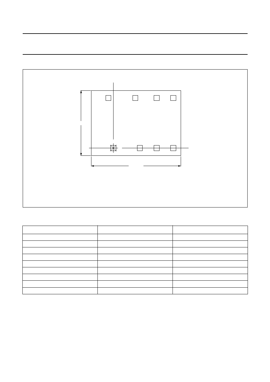
CHIP DIMENSIONS AND BONDING PAD LOCATIONS
Table 3
Bonding pad locations (dimensions in
µ
m)
All x/y coordinates are referenced to bottom left pad (V
DD
), see Fig.11.
PAD
x
y
V
SS
1290
1100
TEST
940
1100
OSC IN
481
1100
OSC OUT
-
102
1100
V
DD
0
0
M1
578
0
M2
930
0
RESET
1290
0
chip corner (max. value)
-
497.5
-
170
Fig.11 Bonding pad locations, PCA146xU series; 8 terminals.
Chip area: 2.91 mm
2
.
Bonding pad dimensions: 110
µ
m
◊
110
µ
m.
Chip thickness: 200
±
25
µ
m, with bumps: 270
±
25
µ
m.
MSA938
0
0
1.44 mm
VDD
M1
M2
RESET
VSS
TEST
OSC IN
OSC OUT
y
x
2.02 mm
PCA146xU
SERIES
1998 Apr 21
18
Philips Semiconductors
Product specification
32 kHz watch circuits with adaptive motor
pulse
PCA146x series
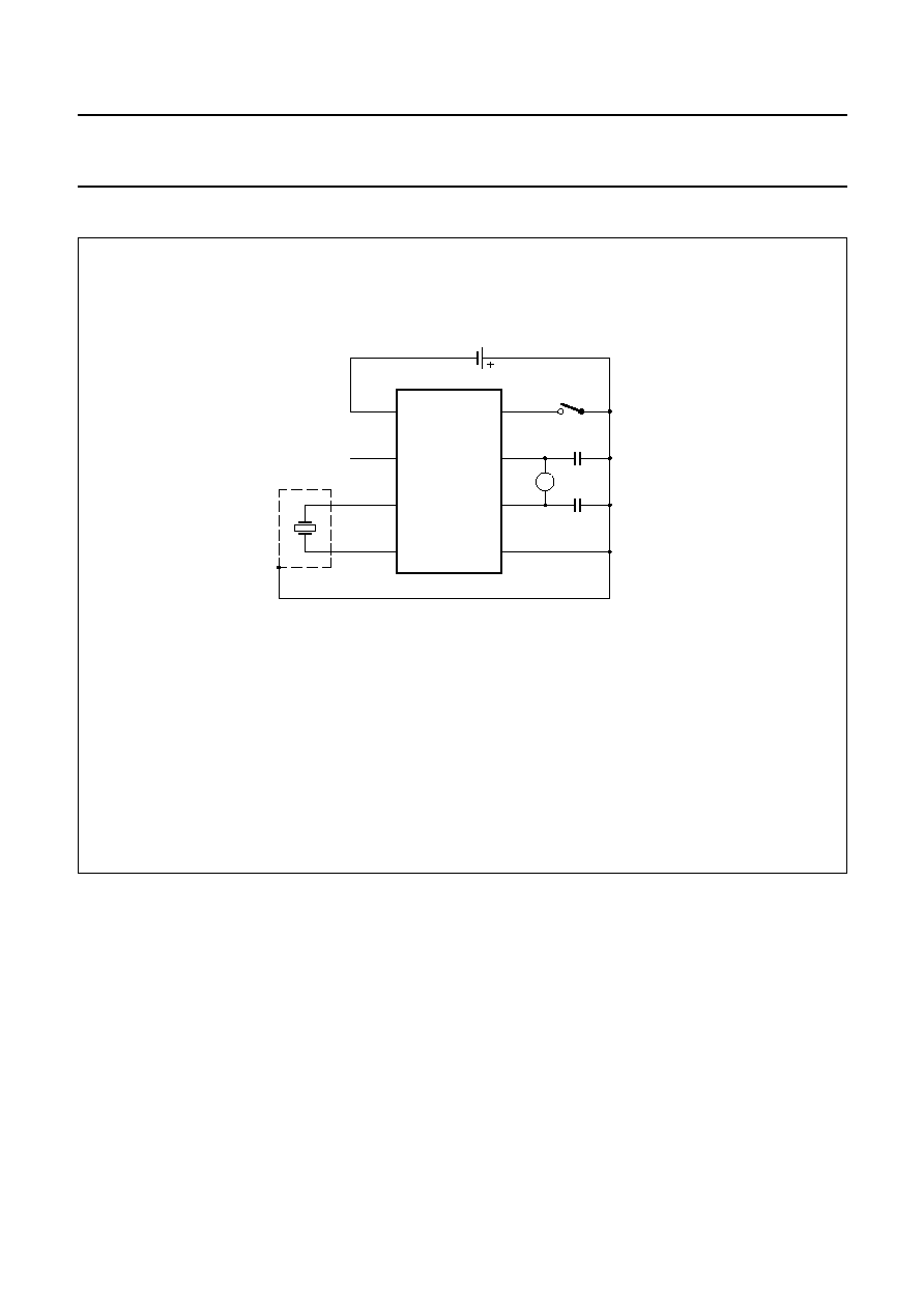
APPLICATION INFORMATION
Fig.12 Typical application circuit diagram.
(1) Quartz crystal case should be connected to V
DD
. Stray capacitance and leakage resistance from RESET, M1 or M2 to OSC IN should be less than
0.5 pF or larger than 20 M
.
(2) Motor, probe and stray capacitance from M2 or M1 to V
DD
or V
SS
should be less than C
M
= 80 pF for correct operation of the detection circuit.
Driving the motor at its minimum energy, probe and stray capacitance must be avoided.
handbook, full pagewidth
MSA939
VDD
M1
M2
RESET
VSS
TEST
OSC IN
OSC OUT
C M
(2)
C M
(2)
M
(1)
1.55 V
PCA146x
SERIES
1
2
3
4
8
7
6
5
1998 Apr 21
19
Philips Semiconductors
Product specification
32 kHz watch circuits with adaptive motor
pulse
PCA146x series
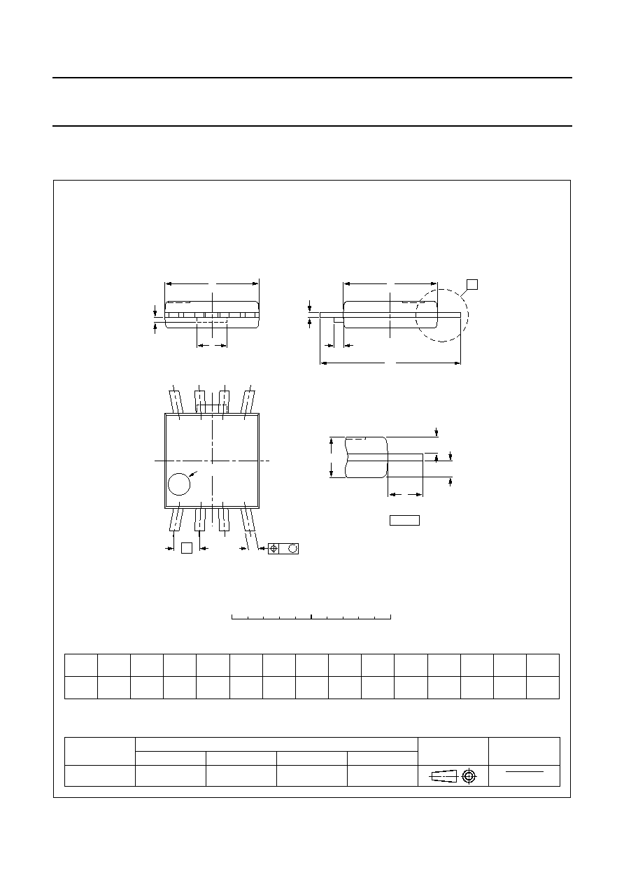
PACKAGE OUTLINE
UNIT
c
e
REFERENCES
OUTLINE
VERSION
EUROPEAN
PROJECTION
ISSUE DATE
IEC
JEDEC
EIAJ
mm
DIMENSIONS (mm are the original dimensions)
SOT144-1
94-01-25
95-01-24
b
n
max.
L
m
max.
H
E
0.40
0.25
0.19
0.12
3.1
2.9
3.1
2.9
4.6
4.4
0.80
0.75
0.26
0.3
Q
1
Q
2
w
t
0.40
0.30
0.1
0.40
0.30
0.95
0.90
0.70
L
w
M
b
Q
2
Q
1
0
2.5
5 mm
scale
Note
1. Plastic or metal protrusions of 0.15 mm maximum per side are not included.
E
(1)
(1)
D
e
t
n
pin 1 index
4
1
5
8
D
E
c
m
X
detail X
PMFP8: plastic micro flat package; 8 leads (straight)
SOT144-1
A
2
A
2
H
E

1998 Apr 21
20
Philips Semiconductors
Product specification
32 kHz watch circuits with adaptive motor
pulse
PCA146x series
SOLDERING
Introduction
There is no soldering method that is ideal for all IC
packages. Wave soldering is often preferred when
through-hole and surface mounted components are mixed
on one printed-circuit board. However, wave soldering is
not always suitable for surface mounted ICs, or for
printed-circuits with high population densities. In these
situations reflow soldering is often used.
This text gives a very brief insight to a complex technology.
A more in-depth account of soldering ICs can be found in
our
"IC Package Databook" (order code 9398 652 90011).
Reflow soldering
Reflow soldering techniques are suitable for all SO
packages.
Reflow soldering requires solder paste (a suspension of
fine solder particles, flux and binding agent) to be applied
to the printed-circuit board by screen printing, stencilling or
pressure-syringe dispensing before package placement.
Several techniques exist for reflowing; for example,
thermal conduction by heated belt. Dwell times vary
between 50 and 300 seconds depending on heating
method. Typical reflow temperatures range from
215 to 250
∞
C.
Preheating is necessary to dry the paste and evaporate
the binding agent. Preheating duration: 45 minutes at
45
∞
C.
Wave soldering
Wave soldering techniques can be used for all SO
packages if the following conditions are observed:
∑
A double-wave (a turbulent wave with high upward
pressure followed by a smooth laminar wave) soldering
technique should be used.
∑
The longitudinal axis of the package footprint must be
parallel to the solder flow.
∑
The package footprint must incorporate solder thieves at
the downstream end.
During placement and before soldering, the package must
be fixed with a droplet of adhesive. The adhesive can be
applied by screen printing, pin transfer or syringe
dispensing. The package can be soldered after the
adhesive is cured.
Maximum permissible solder temperature is 260
∞
C, and
maximum duration of package immersion in solder is
10 seconds, if cooled to less than 150
∞
C within
6 seconds. Typical dwell time is 4 seconds at 250
∞
C.
A mildly-activated flux will eliminate the need for removal
of corrosive residues in most applications.
Repairing soldered joints
Fix the component by first soldering two diagonally-
opposite end leads. Use only a low voltage soldering iron
(less than 24 V) applied to the flat part of the lead. Contact
time must be limited to 10 seconds at up to 300
∞
C. When
using a dedicated tool, all other leads can be soldered in
one operation within 2 to 5 seconds between
270 and 320
∞
C.

1998 Apr 21
21
Philips Semiconductors
Product specification
32 kHz watch circuits with adaptive motor
pulse
PCA146x series
DEFINITIONS
LIFE SUPPORT APPLICATIONS
These products are not designed for use in life support appliances, devices, or systems where malfunction of these
products can reasonably be expected to result in personal injury. Philips customers using or selling these products for
use in such applications do so at their own risk and agree to fully indemnify Philips for any damages resulting from such
improper use or sale.
Data sheet status
Objective specification
This data sheet contains target or goal specifications for product development.
Preliminary specification
This data sheet contains preliminary data; supplementary data may be published later.
Product specification
This data sheet contains final product specifications.
Limiting values
Limiting values given are in accordance with the Absolute Maximum Rating System (IEC 134). Stress above one or
more of the limiting values may cause permanent damage to the device. These are stress ratings only and operation
of the device at these or at any other conditions above those given in the Characteristics sections of the specification
is not implied. Exposure to limiting values for extended periods may affect device reliability.
Application information
Where application information is given, it is advisory and does not form part of the specification.

1998 Apr 21
22
Philips Semiconductors
Product specification
32 kHz watch circuits with adaptive motor
pulse
PCA146x series
NOTES

1998 Apr 21
23
Philips Semiconductors
Product specification
32 kHz watch circuits with adaptive motor
pulse
PCA146x series
NOTES

Internet: http://www.semiconductors.philips.com
Philips Semiconductors ≠ a worldwide company
© Philips Electronics N.V. 1998
SCA57
All rights are reserved. Reproduction in whole or in part is prohibited without the prior written consent of the copyright owner.
The information presented in this document does not form part of any quotation or contract, is believed to be accurate and reliable and may be changed
without notice. No liability will be accepted by the publisher for any consequence of its use. Publication thereof does not convey nor imply any license
under patent- or other industrial or intellectual property rights.
Netherlands: Postbus 90050, 5600 PB EINDHOVEN, Bldg. VB,
Tel. +31 40 27 82785, Fax. +31 40 27 88399
New Zealand: 2 Wagener Place, C.P.O. Box 1041, AUCKLAND,
Tel. +64 9 849 4160, Fax. +64 9 849 7811
Norway: Box 1, Manglerud 0612, OSLO,
Tel. +47 22 74 8000, Fax. +47 22 74 8341
Philippines: Philips Semiconductors Philippines Inc.,
106 Valero St. Salcedo Village, P.O. Box 2108 MCC, MAKATI,
Metro MANILA, Tel. +63 2 816 6380, Fax. +63 2 817 3474
Poland: Ul. Lukiska 10, PL 04-123 WARSZAWA,
Tel. +48 22 612 2831, Fax. +48 22 612 2327
Portugal: see Spain
Romania: see Italy
Russia: Philips Russia, Ul. Usatcheva 35A, 119048 MOSCOW,
Tel. +7 095 755 6918, Fax. +7 095 755 6919
Singapore: Lorong 1, Toa Payoh, SINGAPORE 1231,
Tel. +65 350 2538, Fax. +65 251 6500
Slovakia: see Austria
Slovenia: see Italy
South Africa: S.A. PHILIPS Pty Ltd., 195-215 Main Road Martindale,
2092 JOHANNESBURG, P.O. Box 7430 Johannesburg 2000,
Tel. +27 11 470 5911, Fax. +27 11 470 5494
South America: Al. Vicente Pinzon, 173, 6th floor,
04547-130 S√O PAULO, SP, Brazil,
Tel. +55 11 821 2333, Fax. +55 11 821 2382
Spain: Balmes 22, 08007 BARCELONA,
Tel. +34 3 301 6312, Fax. +34 3 301 4107
Sweden: Kottbygatan 7, Akalla, S-16485 STOCKHOLM,
Tel. +46 8 632 2000, Fax. +46 8 632 2745
Switzerland: Allmendstrasse 140, CH-8027 ZÐRICH,
Tel. +41 1 488 2686, Fax. +41 1 488 3263
Taiwan: Philips Semiconductors, 6F, No. 96, Chien Kuo N. Rd., Sec. 1,
TAIPEI, Taiwan Tel. +886 2 2134 2865, Fax. +886 2 2134 2874
Thailand: PHILIPS ELECTRONICS (THAILAND) Ltd.,
209/2 Sanpavuth-Bangna Road Prakanong, BANGKOK 10260,
Tel. +66 2 745 4090, Fax. +66 2 398 0793
Turkey: Talatpasa Cad. No. 5, 80640 GÐLTEPE/ISTANBUL,
Tel. +90 212 279 2770, Fax. +90 212 282 6707
Ukraine: PHILIPS UKRAINE, 4 Patrice Lumumba str., Building B, Floor 7,
252042 KIEV, Tel. +380 44 264 2776, Fax. +380 44 268 0461
United Kingdom: Philips Semiconductors Ltd., 276 Bath Road, Hayes,
MIDDLESEX UB3 5BX, Tel. +44 181 730 5000, Fax. +44 181 754 8421
United States: 811 East Arques Avenue, SUNNYVALE, CA 94088-3409,
Tel. +1 800 234 7381
Uruguay: see South America
Vietnam: see Singapore
Yugoslavia: PHILIPS, Trg N. Pasica 5/v, 11000 BEOGRAD,
Tel. +381 11 625 344, Fax.+381 11 635 777
For all other countries apply to: Philips Semiconductors,
International Marketing & Sales Communications, Building BE-p, P.O. Box 218,
5600 MD EINDHOVEN, The Netherlands, Fax. +31 40 27 24825
Argentina: see South America
Australia: 34 Waterloo Road, NORTH RYDE, NSW 2113,
Tel. +61 2 9805 4455, Fax. +61 2 9805 4466
Austria: Computerstr. 6, A-1101 WIEN, P.O. Box 213, Tel. +43 160 1010,
Fax. +43 160 101 1210
Belarus: Hotel Minsk Business Center, Bld. 3, r. 1211, Volodarski Str. 6,
220050 MINSK, Tel. +375 172 200 733, Fax. +375 172 200 773
Belgium: see The Netherlands
Brazil: see South America
Bulgaria: Philips Bulgaria Ltd., Energoproject, 15th floor,
51 James Bourchier Blvd., 1407 SOFIA,
Tel. +359 2 689 211, Fax. +359 2 689 102
Canada: PHILIPS SEMICONDUCTORS/COMPONENTS,
Tel. +1 800 234 7381
China/Hong Kong: 501 Hong Kong Industrial Technology Centre,
72 Tat Chee Avenue, Kowloon Tong, HONG KONG,
Tel. +852 2319 7888, Fax. +852 2319 7700
Colombia: see South America
Czech Republic: see Austria
Denmark: Prags Boulevard 80, PB 1919, DK-2300 COPENHAGEN S,
Tel. +45 32 88 2636, Fax. +45 31 57 0044
Finland: Sinikalliontie 3, FIN-02630 ESPOO,
Tel. +358 9 615800, Fax. +358 9 61580920
France: 51 Rue Carnot, BP317, 92156 SURESNES Cedex,
Tel. +33 1 40 99 6161, Fax. +33 1 40 99 6427
Germany: Hammerbrookstraþe 69, D-20097 HAMBURG,
Tel. +49 40 23 53 60, Fax. +49 40 23 536 300
Greece: No. 15, 25th March Street, GR 17778 TAVROS/ATHENS,
Tel. +30 1 4894 339/239, Fax. +30 1 4814 240
Hungary: see Austria
India: Philips INDIA Ltd, Band Box Building, 2nd floor,
254-D, Dr. Annie Besant Road, Worli, MUMBAI 400 025,
Tel. +91 22 493 8541, Fax. +91 22 493 0966
Indonesia: see Singapore
Ireland: Newstead, Clonskeagh, DUBLIN 14,
Tel. +353 1 7640 000, Fax. +353 1 7640 200
Israel: RAPAC Electronics, 7 Kehilat Saloniki St, PO Box 18053,
TEL AVIV 61180, Tel. +972 3 645 0444, Fax. +972 3 649 1007
Italy: PHILIPS SEMICONDUCTORS, Piazza IV Novembre 3,
20124 MILANO, Tel. +39 2 6752 2531, Fax. +39 2 6752 2557
Japan: Philips Bldg 13-37, Kohnan 2-chome, Minato-ku, TOKYO 108,
Tel. +81 3 3740 5130, Fax. +81 3 3740 5077
Korea: Philips House, 260-199 Itaewon-dong, Yongsan-ku, SEOUL,
Tel. +82 2 709 1412, Fax. +82 2 709 1415
Malaysia: No. 76 Jalan Universiti, 46200 PETALING JAYA, SELANGOR,
Tel. +60 3 750 5214, Fax. +60 3 757 4880
Mexico: 5900 Gateway East, Suite 200, EL PASO, TEXAS 79905,
Tel. +9-5 800 234 7381
Middle East: see Italy
Printed in The Netherlands
415108/1200/04/pp24
Date of release: 1998 Apr 21
Document order number:
9397 750 03769