Document Outline
- CONTENTS
- 1 FEATURES
- 1.1 DSP software features
- 2 GENERAL DESCRIPTION
- 3 ORDERING INFORMATION
- 4 BLOCK DIAGRAM
- 5 PINNING INFORMATION
- 5.1 Pinning
- 5.2 Pin description
- 6 FUNCTIONAL DESCRIPTION
- 7 PACKAGE OUTLINE
- 8 SOLDERING
- 9 DEFINITIONS
- 10 LIFE SUPPORT APPLICATIONS
- 11 PURCHASE OF PHILIPS I 2 C COMPONENTS

DATA SHEET
Objective specification
Supersedes data of 1996 Oct 30
File under Integrated Circuits, IC17
1997 Jul 21
INTEGRATED CIRCUITS
PCD5091
DECT baseband controller

1997 Jul 21
2
Philips Semiconductors
Objective specification
DECT baseband controller
PCD5091
CONTENTS
1
FEATURES
1.1
DSP software features
2
GENERAL DESCRIPTION
3
ORDERING INFORMATION
4
BLOCK DIAGRAM
5
PINNING INFORMATION
5.1
Pinning
5.2
Pin description
6
FUNCTIONAL DESCRIPTION
7
PACKAGE OUTLINES
8
SOLDERING
8.1
Introduction
8.2
Reflow soldering
8.3
Wave soldering
8.4
Repairing soldered joints
9
DEFINITIONS
10
LIFE SUPPORT APPLICATIONS
11
PURCHASE OF PHILIPS I
2
C COMPONENTS

1997 Jul 21
3
Philips Semiconductors
Objective specification
DECT baseband controller
PCD5091
1
FEATURES
∑
80C51 ports P0, P1, P2 and P3 available for interfacing
to display, keyboard, I
2
C-bus, interrupt sources and/or
external memory. Integrated 64 kbyte ROM, 3 kbytes of
data memory and 1 kbyte SDR-RAM. External program
memory is addressable up to 128 kbytes
∑
+2.7 to +5 V port (P0 to P3) interface
∑
TDMA frame (de)multiplexing. Transmission or
reception can be programmed for any slot
∑
Ciphering, scrambling, CRC checking/generation and
protected B-fields
∑
Speech and data buffering space for six handsets
∑
Local call and B-field loop-back
∑
Two interrupt lines for BML and DSP to interrupt 80C51
∑
On-chip, three-channel time-multiplexed 8-bit
Analog-to-Digital Converter (ADC) for RSSI
measurement, one for battery voltage measurement
and one channel available for other purposes
∑
On-chip 8-bit Digital-to-Analog Converter (DAC) for
electronic potentiometer function
∑
Phase error measurement and phase error correction by
hardware
∑
DACs and ADCs for dynamic earpiece and dynamic or
electret microphone
∑
On-chip reference voltage
∑
On-chip supply for electret microphone
∑
Very low ohmic buzzer output
∑
Serial interface to external ADPCM CODEC (PCD5032)
or 8 kHz u-law samples
∑
Speech switch for Digital Telephone Answering
Machine (DTAM) connected to SPI interface
∑
IOM-2 interface (Siemens registered trademark)
∑
Serial interface to synthesizer for frequency
programming
∑
Programmable polarity and timing of radio-control
signals
∑
GMSK pulse shaper
∑
Easy interfacing with radio circuits, operating at other
supply voltage (RF supply pin with level shifter for RF
signals)
∑
On-chip comparator for use as data-slicer
∑
Low power oscillator with integrated frequency
adjustment
∑
QFP100 and LQFP100 packages
∑
Power-on-reset
∑
Programmable power-down modes
∑
Low supply voltage (2.7 to 3.6 V)
∑
CMOS technology.
1.1
DSP software features
∑
ADPCM encoding and decoding complying with G.721
∑
Volume control
∑
Speech filters
∑
Programmable gain in speech paths
∑
Side tone and soft mute
∑
Two tone (DTMF) generators
∑
Automatic gain control
∑
Hands-free operation
For each DSP software version a separate manual is
available in which detailed information is provided on how
parameters must be set. For further information please
contact Philips Semiconductors.
2
GENERAL DESCRIPTION
The PCD5091 is designed for GAP-compliant handsets
with speaker-phone option. It has an embedded 80C51
microcontroller with twice the performance of the classic
architecture, 64 kbytes of PROM program memory and
3 kbytes of data memory on-chip. In addition there is
1 kbyte of on-chip data memory that is shared with on-chip
Burst Mode Logic (BML) and DSP, the System Data RAM
(SDR).
3
ORDERING INFORMATION
TYPE
NUMBER
PACKAGE
NAME
DESCRIPTION
VERSION
PCD5091H
QFP100
plastic quad flat package; 100 leads (lead length 1.95 mm);
body 14
◊
20
◊
2.8 mm
SOT317-2
PCD5091HZ
LQFP100
plastic low profile quad flat package; 100 leads; body 14
◊
14
◊
1.4 mm
SOT407-1
1997 Jul 21
4
Philips Semiconductors
Objective specification
DECT baseband controller
PCD5091
4
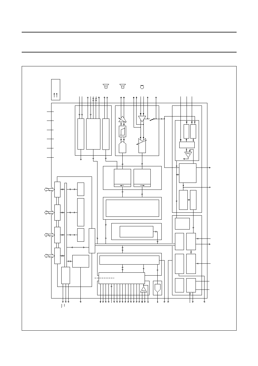
BLOCK DIAGRAM
handbook, full pagewidth
MGD800
R_SLICED
R_DATAM
R_DATAP
T_DATA
T_PWR_RMP
T_ENABLE
ANT_SW1
ANT_SW0
S_PWR
VCO_BND_SW
S_DATA
S_CLK
S_ENABLE
SYNTH_LOCK
REF_CLK
R_ENABLE
R_PWR
SLICE_CTR
LEVEL
SHIFTER
AGM
V
DDA
BURST
MODE
LOGIC
(BML)
CLOCK
GENERATOR
(CLG)
XTAL
OSCILLATOR
(XOSC)
TIMING CONTROL
BLOCK
(TICB)
WATCHDOG
TIMER
(WDT)
ISB BUS
CONTROLLER
(IBC)
RESET
GENERATOR
(RGE)
DIGITAL
CONTROL
OF
ANALOG
(DCA)
80CL51- CORE
ROM
(64 kBYTES)
AB-MICROCONTROLLER
INTERFACE (ABCIF)
PORT 0
8
8
8
8
PORT 1
PORT 2
PORT 3
AUX-RAM
(3 kBYTES)
MICROCONTROLLER-RAM
(256 BYTES)
I
2
C-BUS
SYSTEM
DATA
RAM
(SDR)
(1 kBYTE)
DIGITAL
SIGNAL
PROCESSOR
(DSP)
DIGITAL
DECIMATING
FILTER
(DDF)
DIGITAL
NOISE
SHAPER
(DNS)
4f
s
4f
s
ANALOG VOLTAGE
REFERENCE
(AVR)
POWER-ON-RESET
(POR)
ANALOG
VOLTAGE
SOURCE
(AVS)
PEAK-HOLD
SUBTRACT
MUX
3 : 1
V
ADC
AUXILIARY ADC (AAD)
V
ref
1-BIT ADC
ATS
1-BIT ADC
ARD
ARF
ARA
AMP
V
ref
TEST CONTROL BLOCK
(TCB)
SPEECH INTERFACE
IOM/ADPCM
(SPI)
BUZZER BUFFER
(ABB)
CODEC
V
DD
V
DD
V
DD
V
DD
V
DDA
CDC-on
108f
s
108f
s
V
DD_RF
V
DD
PSE
EA
ALE
A16
V
DD
V
DDA
T_GMSK
DPLL_DATA
GP_CLK7
XTAL1
V
DDO
V
SSO
XTAL2
CLK100
EN_WATCHDOG
RESET_OUT
M_RESET
VBGP
VANLO
VBAT
RSSI_AN
VANLI
V
ref
VMIC
MICM
MICP
LIFM
LIFP
EARM
EARP
BZM
BZP
CLK3
DCK
FS1
DI
DO
TST2
TST1
V
DD_RF
2
◊
V
DD3V
3
◊
V
DD5V
5
◊
V
SS
V
SSA
V
DDA
PORT 0.0 to
PORT 0.7
PORT 1.0 to
PORT 1.7
PORT 2.0 to
PORT 2.7
PORT 3.0 to
PORT 3.7
V
DD
digital pins
analog pins
MICROCONTROLLER
PCD5091
IB-BUS
Fig.1 Block diagram.
1997 Jul 21
5
Philips Semiconductors
Objective specification
DECT baseband controller
PCD5091
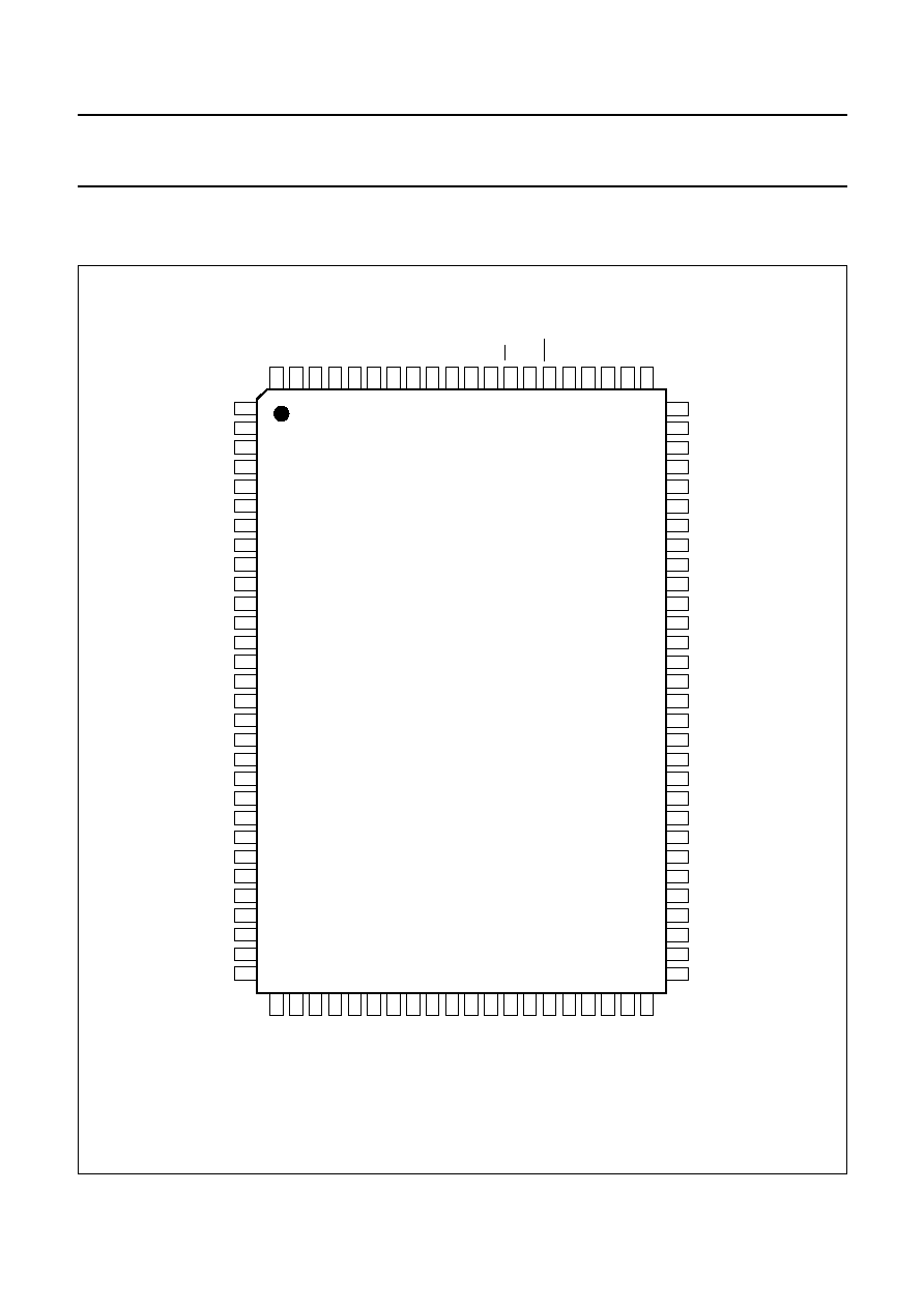
5
PINNING INFORMATION
5.1
Pinning
Fig.2 Pin configuration (QFP100).
handbook, full pagewidth
80
79
78
77
76
75
74
73
72
71
70
69
68
67
66
65
64
63
62
61
60
59
58
57
56
55
54
53
52
51
TST2
TST1
VSS4
VDD5V_2
A16
P2.2
P2.1
P2.0
P3.7
P3.6
P3.5
P3.4
P3.3
P3.2
P3.1
P3.0
VSS3
VSS2
BZP
BZM
VDD3V_2
P1.7
P1.6
P1.5
P1.4
P1.3
VDD5V_1
R_SLICED
DPLL_DATA
GP_CLK7
ANT_SW1
ANT_SW0
CLK100
T_ENABLE
T_PWR_RMP
T_DATA
T_GMSK
VCO_BND_SW
SYNTH_LOCK
S_ENABLE
S_DATA
S_CLK
S_PWR
REF_CLK
VSS1
VDD_RF
VDD3V_1
SLICE_CTR
R_PWR
R_DATAP
R_DATAM
R_ENABLE
RSSI_AN
VANLI
VBAT
CLK3
DCK
DI
FS1
DO
XTAL2
XTAL1
VANLO
V
SSO
V
DDO
LIFM
LIFP
V
SSA
MICM
MICP
VMIC
V
ref
VBGP
V
DDA
EARM
EARP
EN_WATCHDOG
P1.0
P1.1
P1.2
RESET_OUT
M_RESET
P0.0
P0.1
P0.2
P0.3
P0.4
P0.5
P0.6
P0.7
V
DD5V_3
V
SS5
EA
ALE
PSE
P2.7
P2.6
P2.5
P2.4
P2.3
30
29
28
27
26
25
24
23
22
21
20
19
18
17
16
15
14
13
12
11
10
9
8
7
6
5
4
3
2
1
100
99
98
97
96
95
94
93
92
91
90
89
88
87
86
85
84
83
82
81
31
32
33
34
35
36
37
38
39
40
41
42
43
44
45
46
47
48
49
50
MBH938
PCD5091
1997 Jul 21
6
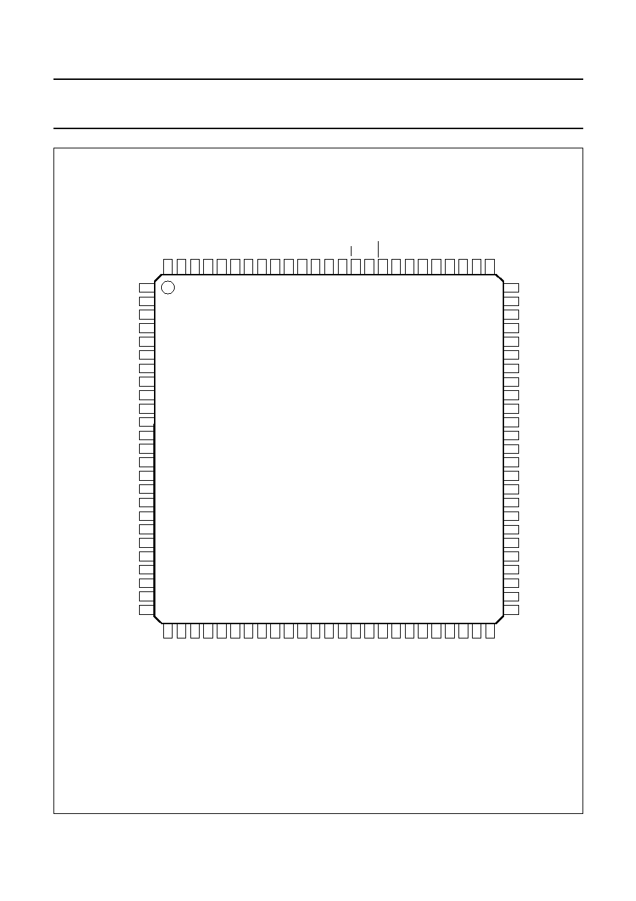
Philips Semiconductors
Objective specification
DECT baseband controller
PCD5091
Fig.3 Pin configuration (LQFP100).
handbook, full pagewidth
75
74
73
72
71
70
69
68
67
66
65
64
63
62
61
60
59
58
57
56
55
54
53
52
51
25
24
23
22
21
20
19
18
17
16
15
14
13
12
11
10
9
8
7
6
5
4
3
2
1
100
99
98
97
96
95
94
93
92
91
90
89
88
87
86
85
84
83
82
81
80
79
78
77
76
26
27
28
29
30
31
32
33
34
35
36
37
38
39
40
41
42
43
44
45
46
47
48
49
50
MGD798
PCD5091
TST2
TST1
V
SS4
VDD5V_2
A16
P2.2
P2.1
P2.0
P3.7
P3.6
P3.5
P3.4
P3.3
P3.2
P3.1
P3.0
VSS3
VSS2
BZP
BZM
VDD3V_2
P1.7
P1.6
P1.5
P1.4
P1.3
VDD5V_1
R_SLICED
DPLL_DATA
GP_CLK7
ANT_SW1
ANT_SW0
CLK100
T_ENABLE
T_PWR_RMP
T_DATA
T_GMSK
VCO_BND_SW
SYNTH_LOCK
S_ENABLE
S_DATA
S_CLK
S_PWR
REF_CLK
VSS1
VDD_RF
VDD3V_1
SLICE_CTR
R_PWR
R_DATAP
R_DATAM
R_ENABLE
RSSI_AN
VANLI
VBAT
CLK3
DCK
DI
FS1
DO
XTAL2
XTAL1
VANLO
V
SSO
V
DDO
LIFM
LIFP
V
SSA
MICM
MICP
VMIC
V
ref
VBGP
V
DDA
EARM
EARP
EN_WATCHDOG
P1.0
P1.1
P1.2
RESET_OUT
M_RESET
P0.0
P0.1
P0.2
P0.3
P0.4
P0.5
P0.6
P0.7
V
DD5V_3
V
SS5
EA
ALE
PSE
P2.7
P2.6
P2.5
P2.4
P2.3

1997 Jul 21
7
Philips Semiconductors
Objective specification
DECT baseband controller
PCD5091
5.2
Pin description
Table 1
QFP100 and LQFP100 packages
SYMBOL
PIN
I/O
STATE
AFTER
RESET
PIN TYPE
PIN DESCRIPTION
QFP100 LQFP100
ANT_SW1
1
99
O
H
ISP2DRF3
antenna switch 1 output
ANT_SW0
2
100
O
H
ISP2DRF3
antenna switch 0 output
CLK100
3
1
O
H
ISP2DPES
100 Hz signal related to DECT frame timing
output
T_ENABLE
4
2
O
H
ISP2DRF3
enable transmitter output
T_PWR_RMP
5
3
O
L
ISP2DRF3
switch transmitter power output
T_DATA
6
4
O
off
ISF2DRF3
unmodulated transmitter data output
T_GMSK
7
5
O
L
ANAIOD1
GMSK modulated transmitter data output
VCO_BND_SW
8
6
O
L
ISP2DRF3
VCO band switch output
SYNTH_LOCK
9
7
I
-
DIPP0RF3
synthesizer lock input
S_ENABLE
10
8
O
L
ISP2DRF3
synthesizer enable output
S_DATA
11
9
O
L
ISP2DRF3
serial synthesizer data output
S_CLK
12
10
O
L
ISP2DRF3
clock for serial synthesizer interface output
S_PWR
13
11
O
H
ISP2DRF3
switch synthesizer power output
REF_CLK
14
12
O
running
ISP4DRF3
13.824 MHz reference clock for synthesizer
output
V
SS1
15
13
-
-
supply
negative supply voltage 1
V
DD_RF
16
14
-
-
supply
positive supply voltage for RF interface level
shifters
V
DD3V_1
17
15
-
-
supply
positive supply voltage 1 (+3 V)
SLICE_CTR
18
16
O
L
ISP2DRF3
switch slicer time constant output
R_PWR
19
17
O
H
ISP2DRF3
switch receiver power output
R_DATAP
20
18
I
-
ANAIOD2
positive input for receiver data
R_DATAM
21
19
I
-
ANAIOD2
negative input for receiver data
R_ENABLE
22
20
O
H
ISP2DRF3
enable receiver output
RSSI_AN
23
21
I
-
ANAIOD1
analog input for RSSI measurement
VANLI
24
22
I
-
ANAIOD1
analog input to ADC
VBAT
25
23
I
-
ANAIOD1
analog input for battery voltage
measurement
CLK3
26
24
O
L
ISP2DPES
3.456 MHz clock output for external ADPCM
codec

1997 Jul 21
8
Philips Semiconductors
Objective specification
DECT baseband controller
PCD5091
DCK
27
25
I/O
input
ISF2DPES
ISF2UPES
ADPCM output or IOM data clock
input/output (ISF2UPES in PCD5090/xxx,
PCA5097/xxx)
DI
28
26
I
-
DIPP0PES
ADPCM or IOM data input
FS1
29
27
I/O
input
ISF2DPES
ISF2UPES
8 kHz framing input/output
(ISF2UPES in PCD5090/xxx, PCA5097/xxx)
DO
30
28
O
off
ISI8DPES
ADPCM or IOM data output
XTAL2
31
29
O
running
ANAIOD1
crystal oscillator output
XTAL1
32
30
I
-
ANAIOD1
crystal oscillator input
VANLO
33
31
O
1.0 V
ANAIOD1
analog output from D/A converter
V
SSO
34
32
-
-
supply
negative supply voltage for the oscillator
V
DDO
35
33
-
-
supply
positive supply voltage for the oscillator
LIFM
36
34
I
0.7 V
ANAIOD1
negative input from line interface
LIFP
37
35
I
0.7 V
ANAIOD1
positive input from line interface
V
SSA
38
36
-
-
supply
negative supply voltage for analog circuits
MICM
39
37
I
0.7 V
ANAIOR1
negative input from microphone
MICP
40
38
I
0.7 V
ANAIOR1
positive input from microphone
VMIC
41
39
O
off
ANAIOD1
positive microphone supply voltage (+2 V)
V
ref
42
40
O
2.0 V
ANAIOD1
reference voltage (+2 V)
VBGP
43
41
O
1.25 V
ANAIOR1
bandgap output voltage (+1.25 V)
V
DDA
44
42
-
-
supply
positive supply voltage for analog circuits
EARM
45
43
O
1.4 V
ANAIOD1
negative output to earpiece
EARP
46
44
O
1.4 V
ANAIOD1
positive output to earpiece
EN_WATCHDOG
47
45
I
-
DIUP0PES
watchdog enable input
P1.0
48
46
I/O
H
ISQ2CPES
bidirectional 80C51 port pin
P1.1
49
47
I/O
H
ISQ2CPES
bidirectional 80C51 port pin
P1.2
50
48
I/O
H
ISQ2CPES
bidirectional 80C51 port pin
GP_CLK7
51
49
O
L
ISP2DPES
general purpose 6.912 MHz output
DPLL_DATA
52
50
O
L
ISP2DPES
data after clock recovery network
R_SLICED
53
51
O
L
ISP2DPES
R_DATA comparator output
V
DD5V_1
54
52
-
-
supply
positive supply voltage 1 for the +5 V
interface
P1.3
55
53
I/O
H
ISQ2CPES
bidirectional 80C51 port pin
P1.4
56
54
I/O
H
ISQ2CPES
bidirectional 80C51 port pin
SYMBOL
PIN
I/O
STATE
AFTER
RESET
PIN TYPE
PIN DESCRIPTION
QFP100 LQFP100

1997 Jul 21
9
Philips Semiconductors
Objective specification
DECT baseband controller
PCD5091
P1.5
57
55
I/O
H
ISQ2CPES
bidirectional 80C51 port pin
P1.6
58
56
I/O
off
ISI8DPES
bidirectional 80C51 port pin
P1.7
59
57
I/O
off
ISI8DPES
bidirectional 80C51 port pin
V
DD3V_2
60
58
-
-
supply
positive supply voltage 2 (+3 V)
BZM
61
59
O
L
ANAIOD2
negative buzzer output
BZP
62
60
O
L
ANAIOD2
positive buzzer output
V
SS2
63
61
-
-
supply
negative supply voltage 2
V
SS3
64
62
-
-
supply
negative supply voltage 3
P3.0
65
63
I/O
H
ISQ2CPES
bidirectional 80C51 port pin
P3.1
66
64
I/O
H
ISQ2CPES
bidirectional 80C51 port pin
P3.2
67
65
I/O
H
ISQ2CPES
bidirectional 80C51 port pin
P3.3
68
66
I/O
H
ISQ2CPES
bidirectional 80C51 port pin
P3.4
69
67
I/O
H
ISQ2CPES
bidirectional 80C51 port pin
P3.5
70
68
I/O
H
ISQ2CPES
bidirectional 80C51 port pin
P3.6
71
69
I/O
H
ISQ2CPES
bidirectional 80C51 port pin
P3.7
72
70
I/O
H
ISQ2CPES
bidirectional 80C51 port pin
P2.0
73
71
I/O
H
ISQ2CPES
bidirectional 80C51 port pin
P2.1
74
72
I/O
H
ISQ2CPES
bidirectional 80C51 port pin
P2.2
75
73
I/O
H
ISQ2CPES
bidirectional 80C51 port pin
A16
76
74
O
L
ISP4DPES
address bit 16 for 128 kbytes external
program memory
V
DD5V_2
77
75
-
-
supply
positive supply voltage 2 for the +5 V
interface
V
SS4
78
76
-
-
supply
negative supply voltage 4
TST1
79
77
I
-
DIDP0PES
test input 1
TST2
80
78
I
-
DIDP0PES
test input 2
P2.3
81
79
I/O
H
ISQ2CPES
bidirectional 80C51 port pin
P2.4
82
80
I/O
H
ISQ2CPES
bidirectional 80C51 port pin
P2.5
83
81
I/O
H
ISQ2CPES
bidirectional 80C51 port pin
P2.6
84
82
I/O
H
ISQ2CPES
bidirectional 80C51 port pin
P2.7
85
83
I/O
H
ISQ2CPES
bidirectional 80C51 port pin
PSE
86
84
O
H
ISQ2CPES
program store enable (80C51); active LOW
ALE
87
85
O
H
ISQ4CPES
address latch enable (80C51)
SYMBOL
PIN
I/O
STATE
AFTER
RESET
PIN TYPE
PIN DESCRIPTION
QFP100 LQFP100

1997 Jul 21
10
Philips Semiconductors
Objective specification
DECT baseband controller
PCD5091
EA
88
86
I
-
ISF2DPES
external access enable (80C51); active
LOW
V
SS5
89
87
-
-
supply
negative supply voltage 5
V
DD5V_3
90
88
-
-
supply
positive supply voltage 3 for the +5 V
interface
P0.7
91
89
I/O
off
H
ISP2DPES
ISQ2CPES
bidirectional 80C51 port pin
(ISQ2CPES in PCD5090/xxx,
PCA5097/xxx)
P0.6
92
90
I/O
off
H
ISP2DPES
ISQ2CPES
bidirectional 80C51 port pin
(ISQ2CPES in PCD5090/xxx,
PCA5097/xxx)
P0.5
93
91
I/O
off
H
ISP2DPES
ISQ2CPES
bidirectional 80C51 port pin
(ISQ2CPES in PCD5090/xxx,
PCA5097/xxx)
P0.4
94
92
I/O
off
H
ISP2DPES
ISQ2CPES
bidirectional 80C51 port pin
(ISQ2CPES in PCD5090/xxx,
PCA5097/xxx)
P0.3
95
93
I/O
off
H
ISP2DPES
ISQ2CPES
bidirectional 80C51 port pin
(ISQ2CPES in PCD5090/xxx,
PCA5097/xxx)
P0.2
96
94
I/O
off
H
ISP2DPES
ISQ2CPES
bidirectional 80C51 port pin
(ISQ2CPES in PCD5090/xxx,
PCA5097/xxx)
P0.1
97
95
I/O
off
H
ISP2DPES
ISQ2CPES
bidirectional 80C51 port pin
(ISQ2CPES in PCD5090/xxx,
PCA5097/xxx)
P0.0
98
96
I/O
off
H
ISP2DPES
ISQ2CPES
bidirectional 80C51 port pin
(ISQ2CPES in PCD5090/xxx,
PCA5097/xxx)
M_RESET
99
97
I
-
DIDP0PES
master reset input (Schmitt trigger)
RESET_OUT
100
98
O
H
ISF2DPES
reset output
SYMBOL
PIN
I/O
STATE
AFTER
RESET
PIN TYPE
PIN DESCRIPTION
QFP100 LQFP100
1997 Jul 21
11
Philips Semiconductors
Objective specification
DECT baseband controller
PCD5091
6
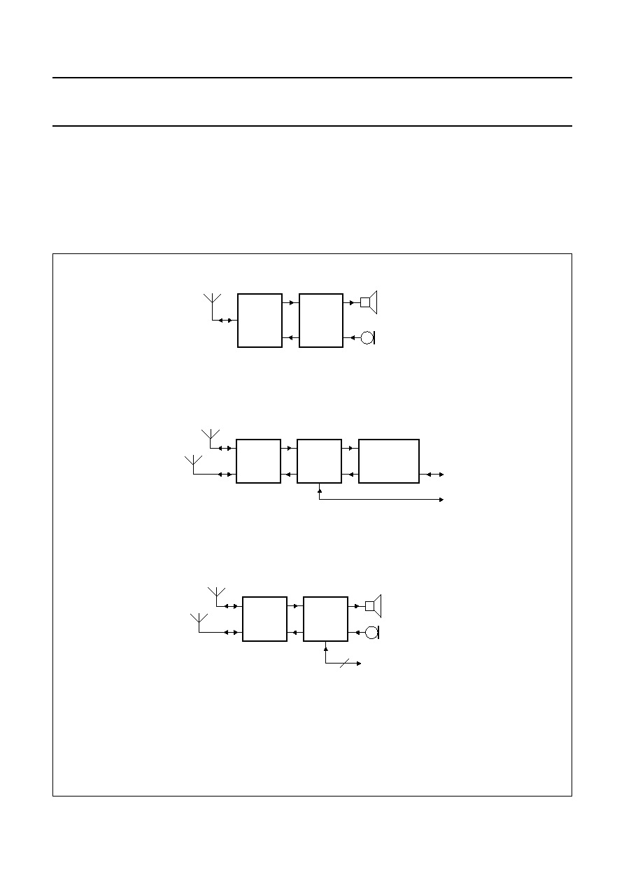
FUNCTIONAL DESCRIPTION
The PCD509x is a family of single-chip controllers, designed for use in Digital Enhanced Cordless Telecommunications
systems (DECT). The family is designed for minimum component-count and minimum power consumption. All controllers
include an embedded 80C51 microcontroller with on-chip memory and I
2
C-bus. The Philips DECT RF interface is
implemented. The Burst Mode Logic (BML) performs the time-critical MAC layer functions for applications in DECT
handsets and base stations. The ADPCM transcoding is in compliance with the CCITT recommendation G.721 and
includes receive and transmit filters.
handbook, full pagewidth
PCD5092/
PCD5094
MBH945
LINE
INTERFACE
(e.g. TEA1118)
a/b line
u-law TAM switch
RADIO
CIRCUITS
Fig.4 Block diagrams of DECT systems with PCX509x.
a. Handset.
b. Base with analog interface and echo cancellation; up to 6 portables can be handled.
c. Base with digital interface and analog handset connected; up to 6 portables can be handled.
handbook, full pagewidth
MGD797
MICROPHONE
EARPIECE
PCD5091
RADIO
CIRCUITS
handbook, full pagewidth
PCD5093
MGD795
MICROPHONE
EARPIECE
RADIO
CIRCUITS
2
2 x IOM or
2 x ADPCM-CODEC or
a combination
1997 Jul 21
12
Philips Semiconductors
Objective specification
DECT baseband controller
PCD5091
7
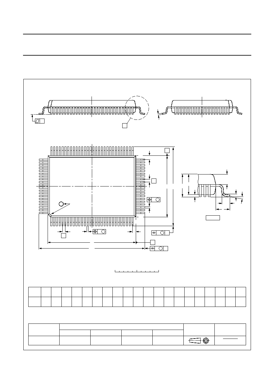
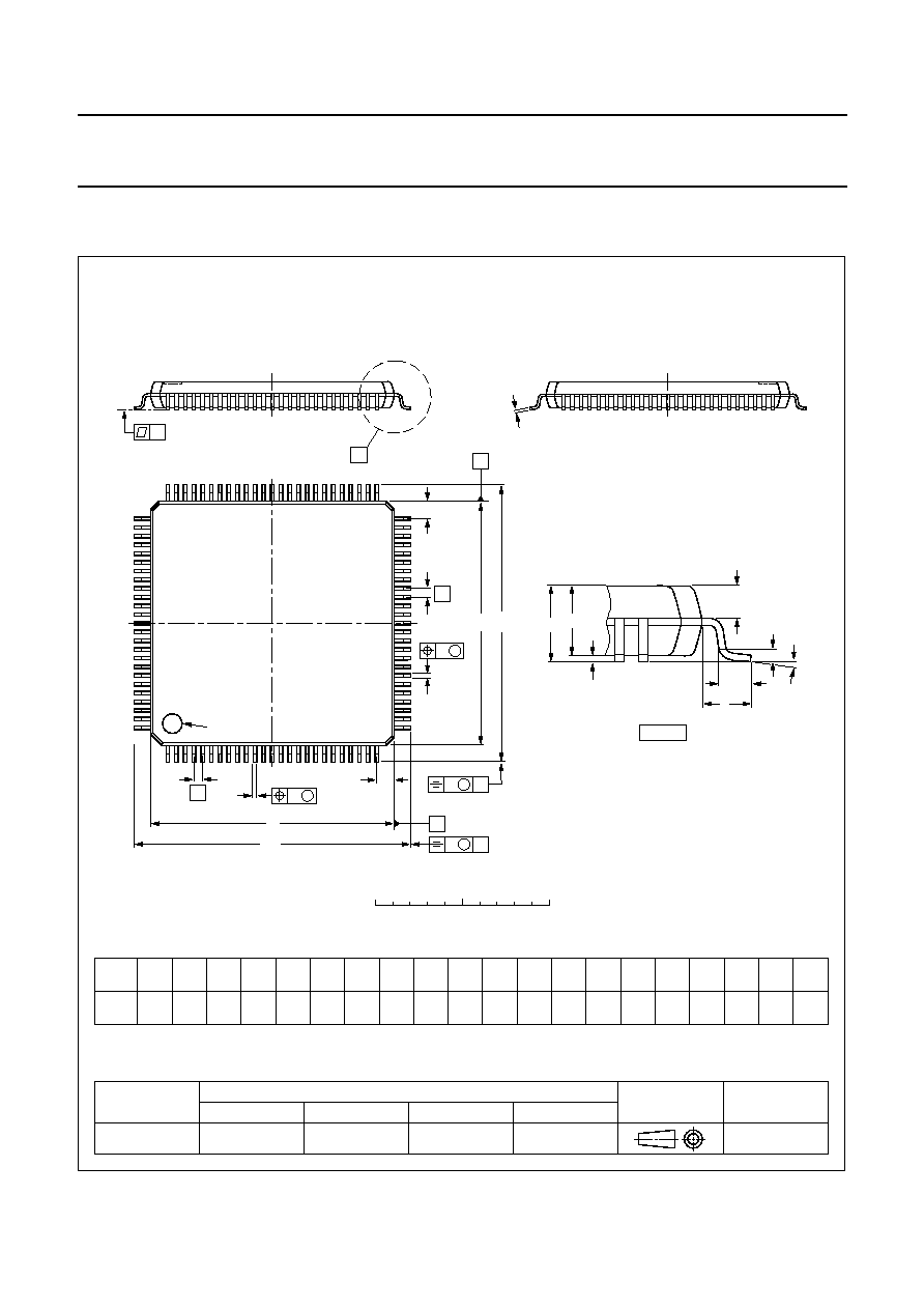
PACKAGE OUTLINE
UNIT
A
1
A
2
A
3
b
p
c
E
(1)
e
H
E
L
L
p
Q
Z
y
w
v
REFERENCES
OUTLINE
VERSION
EUROPEAN
PROJECTION
ISSUE DATE
IEC
JEDEC
EIAJ
mm
0.25
0.05
2.90
2.65
0.25
0.40
0.25
0.25
0.14
14.1
13.9
0.65
18.2
17.6
1.4
1.2
1.0
0.6
7
0
o
o
0.15
0.1
0.2
1.95
DIMENSIONS (mm are the original dimensions)
Note
1. Plastic or metal protrusions of 0.25 mm maximum per side are not included.
1.0
0.6
SOT317-2
92-11-17
95-02-04
D
(1)
(1)
(1)
20.1
19.9
H
D
24.2
23.6
E
Z
0.8
0.4
D
e
E
A
1
A
L
p
Q
detail X
L
(A )
3
B
30
c
b
p
E
H
A
2
D
Z D
A
Z E
e
v
M
A
1
100
81
80
51
50
31
pin 1 index
X
y
b
p
D
H
v
M
B
w
M
w
M
0
5
10 mm
scale
QFP100: plastic quad flat package; 100 leads (lead length 1.95 mm); body 14 x 20 x 2.8 mm
SOT317-2
A
max.
3.20
1997 Jul 21
13
Philips Semiconductors
Objective specification
DECT baseband controller
PCD5091
UNIT
A
max.
A
1
A
2
A
3
b
p
c
E
(1)
e
H
E
L
L
p
Q
Z
y
w
v
REFERENCES
OUTLINE
VERSION
EUROPEAN
PROJECTION
ISSUE DATE
IEC
JEDEC
EIAJ
mm
1.6
0.20
0.05
1.5
1.3
0.25
0.28
0.16
0.18
0.12
14.1
13.9
0.5
16.25
15.75
0.70
0.57
1.15
0.85
7
0
o
o
0.12
0.1
0.2
1.0
DIMENSIONS (mm are the original dimensions)
Note
1. Plastic or metal protrusions of 0.25 mm maximum per side are not included.
0.75
0.45
SOT407-1
95-12-19
D
(1)
(1)
(1)
14.1
13.9
H
D
16.25
15.75
E
Z
1.15
0.85
D
b
p
e
E
A
1
A
L
p
Q
detail X
L
(A )
3
B
25
c
D
H
b
p
E
H
A
2
v
M
B
D
ZD
A
Z E
e
v
M
A
X
1
100
76
75
51
50
26
y
pin 1 index
w
M
w
M
0
5
10 mm
scale
LQFP100: plastic low profile quad flat package; 100 leads; body 14 x 14 x 1.4 mm
SOT407-1

1997 Jul 21
14
Philips Semiconductors
Objective specification
DECT baseband controller
PCD5091
8
SOLDERING
8.1
Introduction
There is no soldering method that is ideal for all IC
packages. Wave soldering is often preferred when
through-hole and surface mounted components are mixed
on one printed-circuit board. However, wave soldering is
not always suitable for surface mounted ICs, or for
printed-circuits with high population densities. In these
situations reflow soldering is often used.
This text gives a very brief insight to a complex technology.
A more in-depth account of soldering ICs can be found in
our
"IC Package Databook" (order code 9398 652 90011).
8.2
Reflow soldering
Reflow soldering techniques are suitable for all LQFP and
QFP packages.
The choice of heating method may be influenced by larger
plastic QFP packages (44 leads, or more). If infrared or
vapour phase heating is used and the large packages are
not absolutely dry (less than 0.1% moisture content by
weight), vaporization of the small amount of moisture in
them can cause cracking of the plastic body. For more
information, refer to the Drypack chapter in our
"Quality
Reference Handbook" (order code 9397 750 00192).
Reflow soldering requires solder paste (a suspension of
fine solder particles, flux and binding agent) to be applied
to the printed-circuit board by screen printing, stencilling or
pressure-syringe dispensing before package placement.
Several techniques exist for reflowing; for example,
thermal conduction by heated belt. Dwell times vary
between 50 and 300 seconds depending on heating
method. Typical reflow temperatures range from
215 to 250
∞
C.
Preheating is necessary to dry the paste and evaporate
the binding agent. Preheating duration: 45 minutes at
45
∞
C.
8.3
Wave soldering
Wave soldering is not recommended for LQFP or QFP
packages. This is because of the likelihood of solder
bridging due to closely-spaced leads and the possibility of
incomplete solder penetration in multi-lead devices.
If wave soldering cannot be avoided, the following
conditions must be observed:
∑
A double-wave (a turbulent wave with high upward
pressure followed by a smooth laminar wave)
soldering technique should be used.
∑
The footprint must be at an angle of 45
∞
to the board
direction and must incorporate solder thieves
downstream and at the side corners.
Even with these conditions:
∑
Do not consider wave soldering LQFP packages
LQFP48 (SOT313-2), LQFP64 (SOT314-2) or
LQFP80 (SOT315-1).
∑
Do not consider wave soldering QFP packages
QFP52 (SOT379-1), QFP100 (SOT317-1),
QFP100 (SOT317-2), QFP100 (SOT382-1) or
QFP160 (SOT322-1).
During placement and before soldering, the package must
be fixed with a droplet of adhesive. The adhesive can be
applied by screen printing, pin transfer or syringe
dispensing. The package can be soldered after the
adhesive is cured.
Maximum permissible solder temperature is 260
∞
C, and
maximum duration of package immersion in solder is
10 seconds, if cooled to less than 150
∞
C within
6 seconds. Typical dwell time is 4 seconds at 250
∞
C.
A mildly-activated flux will eliminate the need for removal
of corrosive residues in most applications.
8.4
Repairing soldered joints
Fix the component by first soldering two diagonally-
opposite end leads. Use only a low voltage soldering iron
(less than 24 V) applied to the flat part of the lead. Contact
time must be limited to 10 seconds at up to 300
∞
C.
When using a dedicated tool, all other leads can be
soldered in one operation within 2 to 5 seconds between
270 and 320
∞
C.
1997 Jul 21
15
Philips Semiconductors
Objective specification
DECT baseband controller
PCD5091
9
DEFINITIONS
10 LIFE SUPPORT APPLICATIONS
These products are not designed for use in life support appliances, devices, or systems where malfunction of these
products can reasonably be expected to result in personal injury. Philips customers using or selling these products for
use in such applications do so at their own risk and agree to fully indemnify Philips for any damages resulting from such
improper use or sale.
11 PURCHASE OF PHILIPS I
2
C COMPONENTS
Data sheet status
Objective specification
This data sheet contains target or goal specifications for product development.
Preliminary specification
This data sheet contains preliminary data; supplementary data may be published later.
Product specification
This data sheet contains final product specifications.
Short-form specification
The data in this specification is extracted from a full data sheet with the same type
number and title. For detailed information see the relevant data sheet or data handbook.
Limiting values
Limiting values given are in accordance with the Absolute Maximum Rating System (IEC 134). Stress above one or
more of the limiting values may cause permanent damage to the device. These are stress ratings only and operation
of the device at these or at any other conditions above those given in the Characteristics sections of the specification
is not implied. Exposure to limiting values for extended periods may affect device reliability.
Application information
Where application information is given, it is advisory and does not form part of the specification.
Purchase of Philips I
2
C components conveys a license under the Philips' I
2
C patent to use the
components in the I
2
C system provided the system conforms to the I
2
C specification defined by
Philips. This specification can be ordered using the code 9398 393 40011.

Internet: http://www.semiconductors.philips.com
Philips Semiconductors ≠ a worldwide company
© Philips Electronics N.V. 1997
SCA55
All rights are reserved. Reproduction in whole or in part is prohibited without the prior written consent of the copyright owner.
The information presented in this document does not form part of any quotation or contract, is believed to be accurate and reliable and may be changed
without notice. No liability will be accepted by the publisher for any consequence of its use. Publication thereof does not convey nor imply any license
under patent- or other industrial or intellectual property rights.
Netherlands: Postbus 90050, 5600 PB EINDHOVEN, Bldg. VB,
Tel. +31 40 27 82785, Fax. +31 40 27 88399
New Zealand: 2 Wagener Place, C.P.O. Box 1041, AUCKLAND,
Tel. +64 9 849 4160, Fax. +64 9 849 7811
Norway: Box 1, Manglerud 0612, OSLO,
Tel. +47 22 74 8000, Fax. +47 22 74 8341
Philippines: Philips Semiconductors Philippines Inc.,
106 Valero St. Salcedo Village, P.O. Box 2108 MCC, MAKATI,
Metro MANILA, Tel. +63 2 816 6380, Fax. +63 2 817 3474
Poland: Ul. Lukiska 10, PL 04-123 WARSZAWA,
Tel. +48 22 612 2831, Fax. +48 22 612 2327
Portugal: see Spain
Romania: see Italy
Russia: Philips Russia, Ul. Usatcheva 35A, 119048 MOSCOW,
Tel. +7 095 755 6918, Fax. +7 095 755 6919
Singapore: Lorong 1, Toa Payoh, SINGAPORE 1231,
Tel. +65 350 2538, Fax. +65 251 6500
Slovakia: see Austria
Slovenia: see Italy
South Africa: S.A. PHILIPS Pty Ltd., 195-215 Main Road Martindale,
2092 JOHANNESBURG, P.O. Box 7430 Johannesburg 2000,
Tel. +27 11 470 5911, Fax. +27 11 470 5494
South America: Rua do Rocio 220, 5th floor, Suite 51,
04552-903 S„o Paulo, S√O PAULO - SP, Brazil,
Tel. +55 11 821 2333, Fax. +55 11 829 1849
Spain: Balmes 22, 08007 BARCELONA,
Tel. +34 3 301 6312, Fax. +34 3 301 4107
Sweden: Kottbygatan 7, Akalla, S-16485 STOCKHOLM,
Tel. +46 8 632 2000, Fax. +46 8 632 2745
Switzerland: Allmendstrasse 140, CH-8027 ZÐRICH,
Tel. +41 1 488 2686, Fax. +41 1 481 7730
Taiwan: Philips Semiconductors, 6F, No. 96, Chien Kuo N. Rd., Sec. 1,
TAIPEI, Taiwan Tel. +886 2 2134 2865, Fax. +886 2 2134 2874
Thailand: PHILIPS ELECTRONICS (THAILAND) Ltd.,
209/2 Sanpavuth-Bangna Road Prakanong, BANGKOK 10260,
Tel. +66 2 745 4090, Fax. +66 2 398 0793
Turkey: Talatpasa Cad. No. 5, 80640 GÐLTEPE/ISTANBUL,
Tel. +90 212 279 2770, Fax. +90 212 282 6707
Ukraine: PHILIPS UKRAINE, 4 Patrice Lumumba str., Building B, Floor 7,
252042 KIEV, Tel. +380 44 264 2776, Fax. +380 44 268 0461
United Kingdom: Philips Semiconductors Ltd., 276 Bath Road, Hayes,
MIDDLESEX UB3 5BX, Tel. +44 181 730 5000, Fax. +44 181 754 8421
United States: 811 East Arques Avenue, SUNNYVALE, CA 94088-3409,
Tel. +1 800 234 7381
Uruguay: see South America
Vietnam: see Singapore
Yugoslavia: PHILIPS, Trg N. Pasica 5/v, 11000 BEOGRAD,
Tel. +381 11 625 344, Fax.+381 11 635 777
For all other countries apply to: Philips Semiconductors, Marketing & Sales Communications,
Building BE-p, P.O. Box 218, 5600 MD EINDHOVEN, The Netherlands, Fax. +31 40 27 24825
Argentina: see South America
Australia: 34 Waterloo Road, NORTH RYDE, NSW 2113,
Tel. +61 2 9805 4455, Fax. +61 2 9805 4466
Austria: Computerstr. 6, A-1101 WIEN, P.O. Box 213, Tel. +43 160 1010,
Fax. +43 160 101 1210
Belarus: Hotel Minsk Business Center, Bld. 3, r. 1211, Volodarski Str. 6,
220050 MINSK, Tel. +375 172 200 733, Fax. +375 172 200 773
Belgium: see The Netherlands
Brazil: see South America
Bulgaria: Philips Bulgaria Ltd., Energoproject, 15th floor,
51 James Bourchier Blvd., 1407 SOFIA,
Tel. +359 2 689 211, Fax. +359 2 689 102
Canada: PHILIPS SEMICONDUCTORS/COMPONENTS,
Tel. +1 800 234 7381
China/Hong Kong: 501 Hong Kong Industrial Technology Centre,
72 Tat Chee Avenue, Kowloon Tong, HONG KONG,
Tel. +852 2319 7888, Fax. +852 2319 7700
Colombia: see South America
Czech Republic: see Austria
Denmark: Prags Boulevard 80, PB 1919, DK-2300 COPENHAGEN S,
Tel. +45 32 88 2636, Fax. +45 31 57 0044
Finland: Sinikalliontie 3, FIN-02630 ESPOO,
Tel. +358 9 615800, Fax. +358 9 61580920
France: 4 Rue du Port-aux-Vins, BP317, 92156 SURESNES Cedex,
Tel. +33 1 40 99 6161, Fax. +33 1 40 99 6427
Germany: Hammerbrookstraþe 69, D-20097 HAMBURG,
Tel. +49 40 23 53 60, Fax. +49 40 23 536 300
Greece: No. 15, 25th March Street, GR 17778 TAVROS/ATHENS,
Tel. +30 1 4894 339/239, Fax. +30 1 4814 240
Hungary: see Austria
India: Philips INDIA Ltd, Band Box Building, 2nd floor,
254-D, Dr. Annie Besant Road, Worli, MUMBAI 400 025,
Tel. +91 22 493 8541, Fax. +91 22 493 0966
Indonesia: see Singapore
Ireland: Newstead, Clonskeagh, DUBLIN 14,
Tel. +353 1 7640 000, Fax. +353 1 7640 200
Israel: RAPAC Electronics, 7 Kehilat Saloniki St, PO Box 18053,
TEL AVIV 61180, Tel. +972 3 645 0444, Fax. +972 3 649 1007
Italy: PHILIPS SEMICONDUCTORS, Piazza IV Novembre 3,
20124 MILANO, Tel. +39 2 6752 2531, Fax. +39 2 6752 2557
Japan: Philips Bldg 13-37, Kohnan 2-chome, Minato-ku, TOKYO 108,
Tel. +81 3 3740 5130, Fax. +81 3 3740 5077
Korea: Philips House, 260-199 Itaewon-dong, Yongsan-ku, SEOUL,
Tel. +82 2 709 1412, Fax. +82 2 709 1415
Malaysia: No. 76 Jalan Universiti, 46200 PETALING JAYA, SELANGOR,
Tel. +60 3 750 5214, Fax. +60 3 757 4880
Mexico: 5900 Gateway East, Suite 200, EL PASO, TEXAS 79905,
Tel. +9-5 800 234 7381
Middle East: see Italy
Printed in The Netherlands
437027/00/02/pp16
Date of release: 1997 Jul 21
Document order number:
9397 750 01656