
1.
General description
The SC16C554B/554DB is a 4-channel Universal Asynchronous Receiver and
Transmitter (QUART) used for serial data communications. Its principal function is to
convert parallel data into serial data and vice versa. The UART can handle serial data
rates up to 5 Mbit/s. It comes with an Intel
Æ
or Motorola
Æ
interface.
The SC16C554B/554DB is pin compatible with the ST16C554 and TL16C554 and it will
power-up to be functionally equivalent to the 16C454. Programming of control registers
enables the added features of the SC16C554B/554DB. Some of these added features are
the 16-byte receive and transmit FIFOs, four receive trigger levels. The
SC16C554B/554DB also provides DMA mode data transfers through FIFO trigger levels
and the TXRDY and RXRDY signals. On-board status registers provide the user with error
indications, operational status, and modem interface control. System interrupts may be
tailored to meet user requirements. An internal loop-back capability allows on-board
diagnostics.
The SC16C554B/554DB operates at 5 V, 3.3 V and 2.5 V, and the industrial temperature
range, and is available in plastic PLCC68, LQFP64, and LQFP80 packages.
2.
Features
s
4 channel UART
s
5 V, 3.3 V and 2.5 V operation
s
Industrial temperature range (
-
40
∞
C to +85
∞
C)
s
The SC16C554B is pin and software compatible with the industry-standard
ST16C454/554, ST68C454/554, ST16C554, TL16C554
s
The SC16C554DB is pin and software compatible with ST16C554D, and software
compatible with ST16C454/554, ST16C554, TL16C554
s
Up to 5 Mbit/s data rate at 5 V and 3.3 V, and 3 Mbit/s at 2.5 V
s
5 V tolerant inputs
s
16-byte transmit FIFO
s
16-byte receive FIFO with error flags
s
Programmable auto-RTS and auto-CTS
x
In auto-CTS mode, CTS controls transmitter
x
In auto-RTS mode, RxFIFO contents and threshold control RTS
s
Automatic hardware flow control (RTS/CTS)
s
Software selectable Baud Rate Generator
s
Four selectable Receive FIFO interrupt trigger levels
s
Standard modem interface
SC16C554B/554DB
5 V, 3.3 V and 2.5 V quad UART, 5 Mbit/s (max.) with 16-byte
FIFOs
Rev. 01 -- 9 February 2005
Product data sheet
9397 750 13133
© Koninklijke Philips Electronics N.V. 2005. All rights reserved.
Product data sheet
Rev. 01 -- 9 February 2005
2 of 51
Philips Semiconductors
SC16C554B/554DB
5 V, 3.3 V and 2.5 V quad UART, 5 Mbit/s (max.) with 16-byte FIFOs
s
Standard asynchronous error and framing bits (Start, Stop, and Parity Overrun Break)
s
Transmit, Receive, Line Status, and Data Set interrupts independently controlled
s
Fully programmable character formatting:
x
5, 6, 7, or 8-bit characters
x
Even, Odd, or No-Parity formats
x
1, 1
1
/
2
, or 2-stop bit
x
Baud generation (DC to 5 Mbit/s)
s
False start-bit detection
s
Complete status reporting capabilities
s
3-state output TTL drive capabilities for bi-directional data bus and control bus
s
Line break generation and detection
s
Internal diagnostic capabilities:
x
Loop-back controls for communications link fault isolation
s
Prioritized interrupt system controls
s
Modem control functions (CTS, RTS, DSR, DTR, RI, CD).
3.
Ordering information
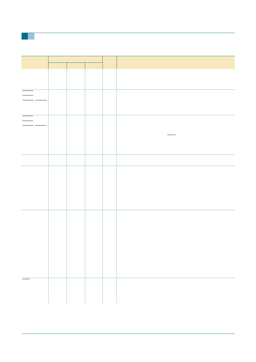
Table 1:
Ordering information
Type number
Package
Name
Description
Version
SC16C554DBIA68
PLCC68
plastic leaded chip carrier; 68 leads
SOT188-2
SC16C554DBIB64
LQFP64
plastic low profile quad flat package; 64 leads; body 10
◊
10
◊
1.4 mm
SOT314-2
SC16C554BIB64
LQFP64
plastic low profile quad flat package; 64 leads; body 10
◊
10
◊
1.4 mm
SOT314-2
SC16C554BIB80
LQFP80
plastic low profile quad flat package; 80 leads; body 12
◊
12
◊
1.4 mm
SOT315-1
9397 750 13133
© Koninklijke Philips Electronics N.V. 2005. All rights reserved.
Product data sheet
Rev. 01 -- 9 February 2005
3 of 51
Philips Semiconductors
SC16C554B/554DB
5 V, 3.3 V and 2.5 V quad UART, 5 Mbit/s (max.) with 16-byte FIFOs
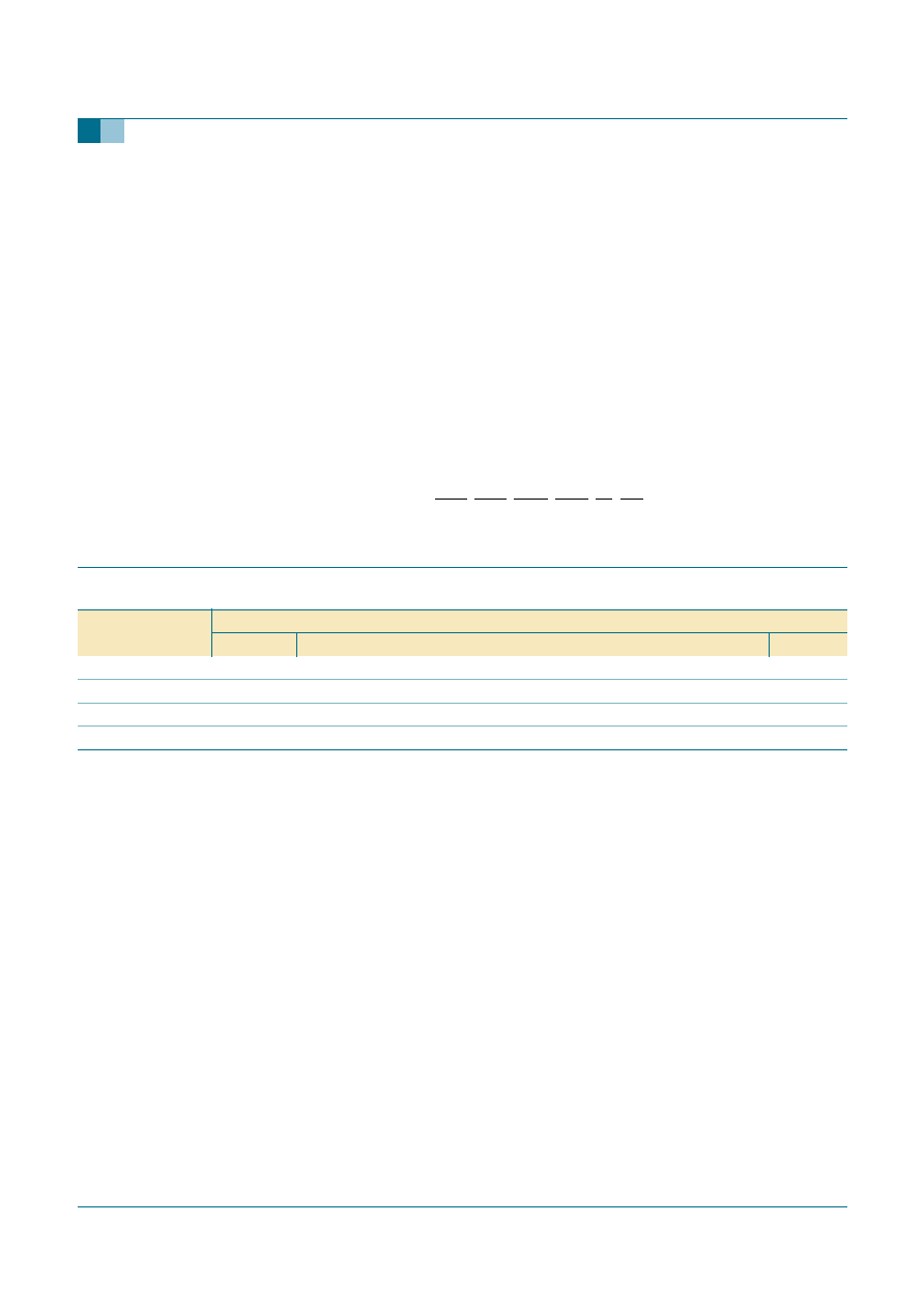
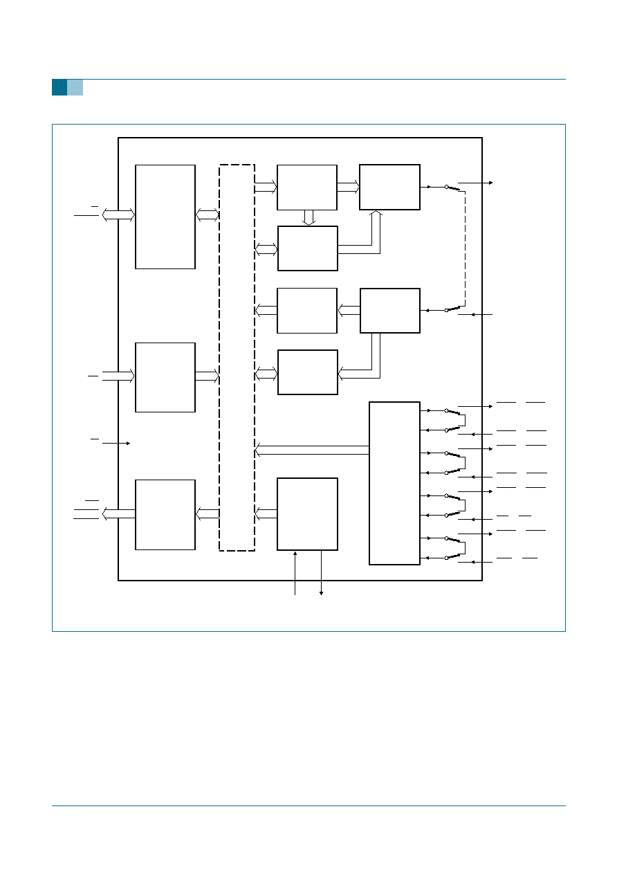
4.
Block diagram
Fig 1.
Block diagram of SC16C554B/554DB (16 mode)
DTRA to DTRD
RTSA to RTSD
TRANSMIT
FIFO
REGISTERS
TXA to TXD
RECEIVE
SHIFT
REGISTER
RECEIVE
FIFO
REGISTERS
RXA to RXD
INTERCONNECT B
US LINES
AND
CONTR
OL SIGNALS
SC16C554B/554DB
TRANSMIT
SHIFT
REGISTER
XTAL2
XTAL1
002aaa877
INTSEL
FLOW
CONTROL
LOGIC
CLKSEL
16/68
DATA BUS
AND
CONTROL
LOGIC
REGISTER
SELECT
LOGIC
INTERRUPT
CONTROL
LOGIC
D0 to D7
IOR
IOW
RESET
A0 to A2
CSA to CSD
INTA to INTD
TXRDY
RXRDY
CLOCK AND
BAUD RATE
GENERATOR
MODEM
CONTROL
LOGIC
CTSA to CTSD
RIA to RID
CDA to CDD
DSRA to DSRD
FLOW
CONTROL
LOGIC
9397 750 13133
© Koninklijke Philips Electronics N.V. 2005. All rights reserved.
Product data sheet
Rev. 01 -- 9 February 2005
4 of 51
Philips Semiconductors
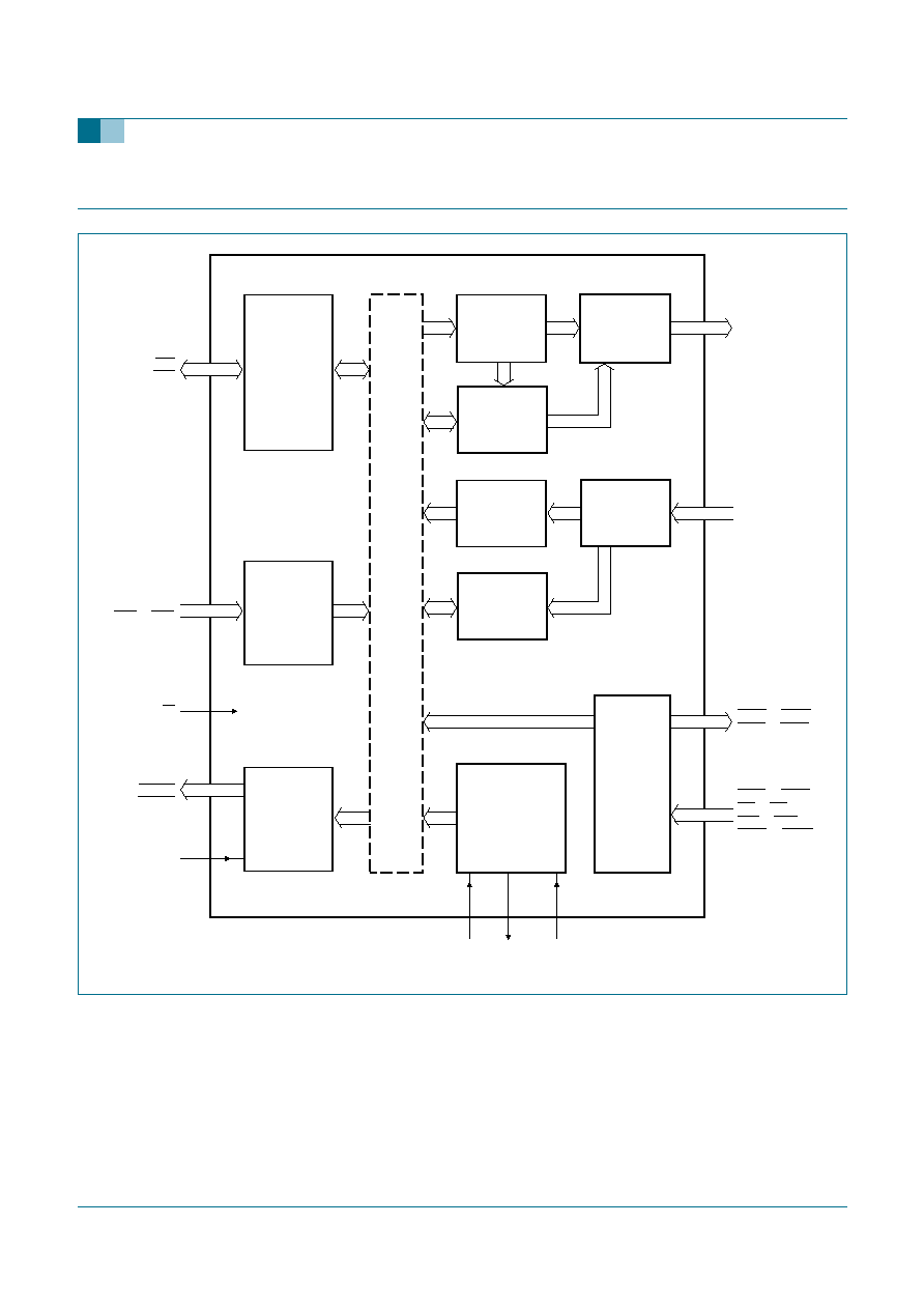
SC16C554B/554DB
5 V, 3.3 V and 2.5 V quad UART, 5 Mbit/s (max.) with 16-byte FIFOs
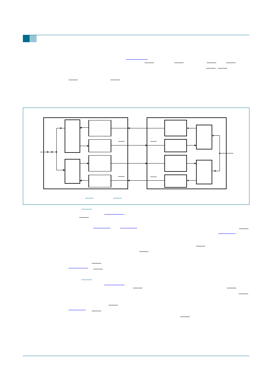
Fig 2.
Block diagram of SC16C554B/554DB (68 mode)
DTRA to DTRD
RTSA to RTSD
TRANSMIT
FIFO
REGISTERS
TXA to TXD
RECEIVE
SHIFT
REGISTER
RECEIVE
FIFO
REGISTERS
RXA to RXD
INTERCONNECT B
US LINES
AND
CONTR
OL SIGNALS
SC16C554B/554DB
TRANSMIT
SHIFT
REGISTER
XTAL2
XTAL1
002aaa878
FLOW
CONTROL
LOGIC
CLKSEL
16/68
DATA BUS
AND
CONTROL
LOGIC
REGISTER
SELECT
LOGIC
INTERRUPT
CONTROL
LOGIC
D0 to D7
R/W
RESET
A0 to A4
CS
IRQ
TXRDY
RXRDY
CLOCK AND
BAUD RATE
GENERATOR
MODEM
CONTROL
LOGIC
CTSA to CTSD
RIA to RID
CDA to CDD
DSRA to DSRD
FLOW
CONTROL
LOGIC
9397 750 13133
© Koninklijke Philips Electronics N.V. 2005. All rights reserved.
Product data sheet
Rev. 01 -- 9 February 2005
5 of 51
Philips Semiconductors
SC16C554B/554DB
5 V, 3.3 V and 2.5 V quad UART, 5 Mbit/s (max.) with 16-byte FIFOs
5.
Pinning information
5.1 Pinning
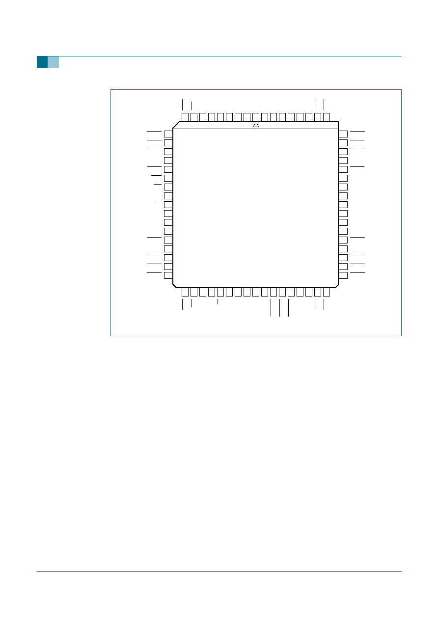
5.1.1 PLCC68
Fig 3.
Pin configuration for PLCC68 (16 mode)
SC16C554DBIA68
16 mode
DSRA
DSRD
CTSA
CTSD
DTRA
DTRD
V
CC
GND
RTSA
RTSD
INTA
INTD
CSA
CSD
TXA
TXD
IOW
IOR
TXB
TXC
CSB
INTB
RTSB
GND
DTRB
CTSB
DSRB
CSC
INTC
RTSC
V
CC
DTRC
CTSC
DSRC
CDB
GND
RIB
D7
RXB
D6
V
CC
D5
CDA
RIA
RXA
n.c.
D4
A2
D3
A1
D2
A0
D1
XTAL1
D0
XTAL2
INTSEL
RESET
RXRDY
TXRDY
GND
RXC
RIC
CDC
V
CC
RXD
RID
CDD
002aaa879
10
11
12
13
14
15
16
17
18
19
20
60
59
58
57
56
55
54
53
52
51
50
21
22
23
24
25
26
49
48
47
46
45
44
27
28
29
30
31
32
33
34
35
36
37
6
5
4
3
2
1
68
67
66
65
64
9
8
7
38
39
40
41
42
43
63
62
61
9397 750 13133
© Koninklijke Philips Electronics N.V. 2005. All rights reserved.
Product data sheet
Rev. 01 -- 9 February 2005
6 of 51
Philips Semiconductors
SC16C554B/554DB
5 V, 3.3 V and 2.5 V quad UART, 5 Mbit/s (max.) with 16-byte FIFOs
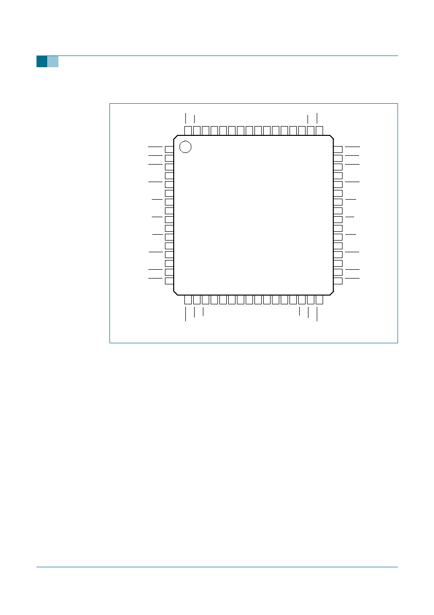
Fig 4.
Pin configuration for PLCC68 (68 mode)
SC16C554DBIA68
68 mode
DSRA
DSRD
CTSA
CTSD
DTRA
DTRD
V
CC
GND
RTSA
RTSD
IRQ
n.c.
CS
n.c.
TXA
TXD
R/W
n.c.
TXB
TXC
A3
n.c.
RTSB
GND
DTRB
CTSB
DSRB
A4
n.c.
RTSC
V
CC
DTRC
CTSC
DSRC
CDB
GND
RIB
D7
RXB
D6
V
CC
D5
CDA
RIA
RXA
16/68
D4
A2
D3
A1
D2
A0
D1
XTAL1
D0
XTAL2
n.c.
RESET
RXRDY
TXRDY
GND
RXC
RIC
CDC
V
CC
RXD
RID
CDD
002aaa880
10
11
12
13
14
15
16
17
18
19
20
60
59
58
57
56
55
54
53
52
51
50
21
22
23
24
25
26
49
48
47
46
45
44
27
28
29
30
31
32
33
34
35
36
37
6
5
4
3
2
1
68
67
66
65
64
9
8
7
38
39
40
41
42
43
63
62
61
9397 750 13133
© Koninklijke Philips Electronics N.V. 2005. All rights reserved.
Product data sheet
Rev. 01 -- 9 February 2005
7 of 51
Philips Semiconductors
SC16C554B/554DB
5 V, 3.3 V and 2.5 V quad UART, 5 Mbit/s (max.) with 16-byte FIFOs
5.1.2 LQFP64
Fig 5.
Pin configuration for LQFP64
SC16C554BIB64
SC16C554DBIB64
INTD
CSD
TXD
IOR
TXC
CSC
INTC
DSRC
002aaa881
1
2
3
4
5
6
7
8
9
10
11
12
13
14
15
16
48
47
46
45
44
43
42
41
40
39
38
37
36
35
34
33
17
18
19
20
21
22
23
24
25
26
27
28
29
30
31
32
64
63
62
61
60
59
58
57
56
55
54
53
52
51
50
49
DSRA
CTSA
DTRA
V
CC
RTSA
INTA
CSA
TXA
IOW
TXB
CSB
INTB
RTSB
GND
DTRB
CTSB
DSRB
CDB
RIB
RXB
V
CC
A2
A1
A0
XTAL1
XTAL2
RESET
GND
RXC
RIC
CDC
DSRD
CTSD
DTRD
GND
RTSD
RTSC
V
CC
DTRC
CTSC
GND
D7
D6
D5
CDA
RIA
RXA
D4
D3
D2
D1
D0
V
CC
RXD
RID
CDD
9397 750 13133
© Koninklijke Philips Electronics N.V. 2005. All rights reserved.
Product data sheet
Rev. 01 -- 9 February 2005
8 of 51
Philips Semiconductors
SC16C554B/554DB
5 V, 3.3 V and 2.5 V quad UART, 5 Mbit/s (max.) with 16-byte FIFOs
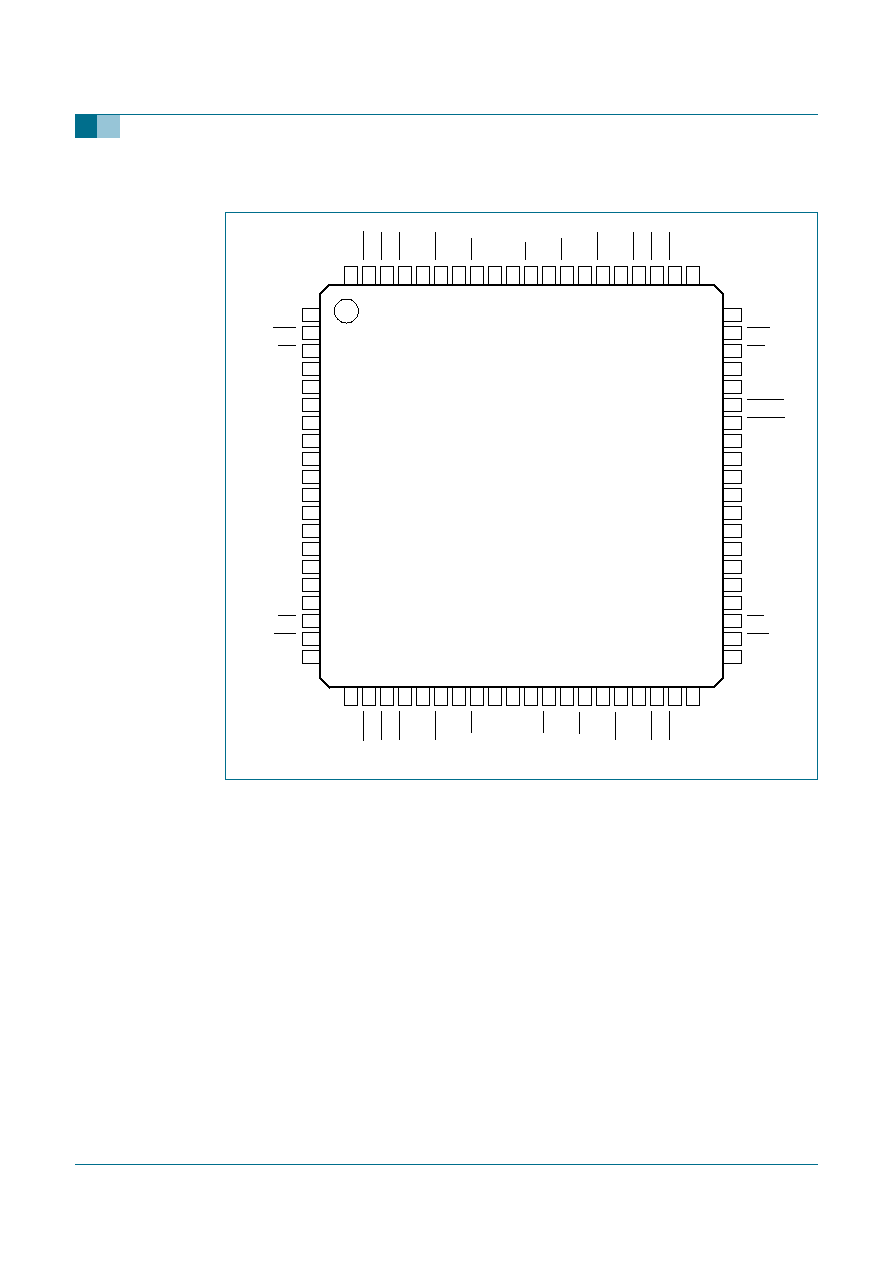
5.1.3 LQFP80
Fig 6.
Pin configuration for LQFP80
SC16C554BIB80
n.c.
CDC
RIC
RXC
GND
TXRDY
D0
RXRDY
D1
RESET
D2
n.c.
n.c.
XTAL2
D3
XTAL1
D4
n.c.
D5
D6
D7
GND
RXA
RIA
CDA
n.c.
n.c.
n.c.
n.c.
DSRD
CTSD
DTRD
GND
RTSD
INTD
CSD
TXD
n.c.
n.c.
IOR
TXC
CSC
INTC
RTSC
V
CC
DTRC
CTSC
DSRC
n.c.
n.c.
1
2
3
4
5
6
7
8
9
10
11
12
13
14
15
16
17
18
19
20
60
59
58
57
56
55
54
53
52
51
50
49
48
47
46
45
44
43
42
41
21
22
23
24
25
26
27
28
29
30
31
32
33
34
35
36
37
38
39
40
80
79
78
77
76
75
74
73
72
71
70
69
68
67
66
65
64
63
62
61
002aaa882
n.c.
CDD
RID
RXD
V
CC
INTSEL
DSRA
CTSA
DTRA
V
CC
RTSA
INTA
CSA
TXA
TXA
IOW
TXB
CSB
INTB
RTSB
GND
DTRB
CTSB
CDB
RIB
RXB
V
CC
A2
A1
A0
9397 750 13133
© Koninklijke Philips Electronics N.V. 2005. All rights reserved.
Product data sheet
Rev. 01 -- 9 February 2005
9 of 51
Philips Semiconductors
SC16C554B/554DB
5 V, 3.3 V and 2.5 V quad UART, 5 Mbit/s (max.) with 16-byte FIFOs
5.2 Pin description
Table 2:
Pin description
Symbol
Pin
Type
Description
PLCC68
LQFP64
LQFP80
16/68
31
-
-
I
16/68 Interface type select (input with internal pull-up). This
input provides the 16 (Intel) or 68 (Motorola) bus interface type
select. The functions of IOR, IOW, INTA to INTD, and CSA to CSD
are re-assigned with the logical state of this pin. When this pin is a
logic 1, the 16 mode interface (16C554) is selected. When this pin
is a logic 0, the 68 mode interface (68C554) is selected. When this
pin is a logic 0, IOW is re-assigned to R/W, RESET is re-assigned
to RESET, IOR is not used, and INTA to INTD are connected in a
wire-OR configuration. The wire-OR outputs are connected
internally to the open drain IRQ signal output. This pin is not
available on 64-pin packages which operate in the 16 mode only.
A0
34
24
48
I
Address 0 select bit. Internal registers address selection in 16 and
68 modes.
A1
33
23
47
I
Address 1 select bit. Internal registers address selection in 16 and
68 modes.
A2
32
22
46
I
Address 2 select bit. Internal registers address selection in 16 and
68 modes.
A3, A4
20, 50
-
-
I
Address 3 to Address 4 select bits. When the 68 mode is
selected, these pins are used to address or select individual UARTs
(providing CS is a logic 0). In the 16 mode, these pins are
re-assigned as chip selects, see CSB and CSC.
CDA, CDB,
CDC, CDD
9, 27,
43, 61
64, 18,
31, 49
19, 42,
59, 2
I
Carrier Detect (active LOW). These inputs are associated with
individual UART channels A through D. A logic 0 on this pin
indicates that a carrier has been detected by the modem for that
channel.
CS
16
-
-
I
Chip Select (active LOW). In the 68 mode, this pin functions as a
multiple channel chip enable. In this case, all four UARTs (A to D)
are enabled when the CS pin is a logic 0. An individual UART
channel is selected by the data contents of address bits A3 to A4.
when the 16 mode is selected (68-pin devices), this pin functions as
CSA (see definition under CSA, CSB).
CSA, CSB,
CSC, CSD
16, 20,
50, 54
7, 11,
38, 42
28, 33,
68, 73
I
Chip Select A, B, C, D (active LOW). This function is associated
with the 16 mode only, and for individual channels `A' through `D'.
When in 16 mode, these pins enable data transfers between the
user CPU and the SC16C554B/554DB for the channel(s)
addressed. Individual UART sections (A, B, C, D) are addressed by
providing a logic 0 on the respective CSA to CSD pin. When the
68 mode is selected, the functions of these pins are re-assigned.
68 mode functions are described under their respective name/pin
headings.
CTSA, CTSB,
CTSC, CTSD
11, 25,
45, 59
2, 16,
33, 47
23, 38,
63, 78
I
Clear to Send (active LOW). These inputs are associated with
individual UART channels A to D. A logic 0 on the CTS pin indicates
the modem or data set is ready to accept transmit data from the
SC16C554B/554DB. Status can be tested by reading MSR[4]. This
pin only affects the transmit or receive operations when auto-CTS
function is enabled via MCR[5] for hardware flow control operation.
9397 750 13133
© Koninklijke Philips Electronics N.V. 2005. All rights reserved.
Product data sheet
Rev. 01 -- 9 February 2005
10 of 51
Philips Semiconductors
SC16C554B/554DB
5 V, 3.3 V and 2.5 V quad UART, 5 Mbit/s (max.) with 16-byte FIFOs
D0 to D2,
D3 to D7
66 to 68,
1 to 5
53 to 55,
56 to 60
7 to 9,
11 to 15
I/O
Data bus (bi-directional). These pins are the 8-bit, 3-state data
bus for transferring information to or from the controlling CPU. D0 is
the least significant bit and the first data bit in a transmit or receive
serial data stream.
DSRA,
DSRB,
DSRC, DSRD
10, 26,
44, 60
1, 17,
32, 48
22, 39,
62, 79
I
Data Set Ready (active LOW). These inputs are associated with
individual UART channels, A through D. A logic 0 on this pin
indicates the modem or data set is powered-on and is ready for data
exchange with the UART. This pin has no effect on the UART's
transmit or receive operation.
DTRA,
DTRB,
DTRC, DTRD
12, 24,
46, 58
3, 15,
34, 46
24, 37,
64, 77
O
Data Terminal Ready (active LOW). These outputs are associated
with individual UART channels, A through D. A logic 0 on this pin
indicates that the SC16C554B/554DB is powered-on and ready.
This pin can be controlled via the modem control register. Writing a
logic 1 to MCR[0] will set the DTR output to logic 0, enabling the
modem. This pin will be a logic 1 after writing a logic 0 to MCR[0], or
after a reset. This pin has no effect on the UART's transmit or
receive operation.
GND
6, 23,
40, 57
14, 28,
45, 61
16, 36,
56, 76
I
Signal and power ground.
INTA, INTB,
INTC, INTD
15, 21,
49, 55
6, 12,
37, 43
27, 34,
67, 74
O
Interrupt A, B, C, D (active HIGH). This function is associated with
the 16 mode only. These pins provide individual channel interrupts
INTA to INTD. INTA to INTD are enabled when MCR[3] is set to a
logic 1, interrupts are enabled in the interrupt enable register (IER),
and when an interrupt condition exists. Interrupt conditions include:
receiver errors, available receiver buffer data, transmit buffer empty,
or when a modem status flag is detected. When the 68 mode is
selected, the functions of these pins are re-assigned. 68 mode
functions are described under their respective name/pin headings.
INTSEL
65
-
6
I
Interrupt Select (active HIGH, with internal pull-down). This
function is associated with the 16 mode only. When the 16 mode is
selected, this pin can be used in conjunction with MCR[3] to enable
or disable the 3-state interrupts, INTA to INTD, or override MCR[3]
and force continuous interrupts. Interrupt outputs are enabled
continuously by making this pin a logic 1. Making this pin a logic 0
allows MCR[3] to control the 3-state interrupt output. In this mode,
MCR[3] is set to a logic 1 to enable the 3-state outputs. This pin is
disabled in the 68 mode. Due to pin limitations on the 64-pin
packages, this pin is not available. To cover this limitation, the
SC16C554DBIB64 version operates in the continuous interrupt
enable mode by bonding this pin to V
CC
internally. The
SC16C554BIB64 operates with MCR[3] control by bonding this pin
to GND.
IOR
52
40
70
I
Input/Output Read strobe (active LOW). This function is
associated with the 16 mode only. A logic 0 transition on this pin will
load the contents of an internal register defined by address bits
A0 to A2 onto the SC16C554B/554DB data bus (D0 to D7) for
access by external CPU. This pin is disabled in the 68 mode.
Table 2:
Pin description
...continued
Symbol
Pin
Type
Description
PLCC68
LQFP64
LQFP80
9397 750 13133
© Koninklijke Philips Electronics N.V. 2005. All rights reserved.
Product data sheet
Rev. 01 -- 9 February 2005
11 of 51
Philips Semiconductors
SC16C554B/554DB
5 V, 3.3 V and 2.5 V quad UART, 5 Mbit/s (max.) with 16-byte FIFOs
IOW
18
9
31
I
Input/Output Write strobe (active LOW). This function is
associated with the 16 mode only. A logic 0 transition on this pin will
transfer the contents of the data bus (D0 to D7) from the external
CPU to an internal register that is defined by address bits A0 to A2.
When the 68 mode is selected, this pin functions as R/W (see
definition under R/W).
IRQ
15
-
-
O
Interrupt Request or Interrupt `A'. This function is associated with
the 68 mode only. In the 68 mode, interrupts from UART channels
A to D are wire-ORed internally to function as a single IRQ
interrupt. This pin transitions to a logic 0 (if enabled by the interrupt
enable register) whenever a UART channel(s) requires service.
Individual channel interrupt status can be determined by addressing
each channel through its associated internal register, using CS and
A3 to A4. In the 68 mode, and external pull-up resistor must be
connected between this pin and V
CC
. The function of this pin
changes to INTA when operating in the 16 mode (see definition
under INTA).
n.c.
21, 49,
52, 54,
55, 65
-
1, 10,
20, 21,
30, 40,
41, 49,
52, 60,
61, 71,
80
-
not connected
RESET
(RESET)
37
27
53
I
Reset. In the 16 mode, a logic 1 on this pin will reset the internal
registers and all the outputs. The UART transmitter output and the
receiver input will be disabled during reset time. (See
Section 7.10
"SC16C554B/554DB external reset conditions"
for initialization
details.) When 16/68 is a logic 0 (68 mode), this pin functions
similarly, bus as an inverted reset interface signal, RESET.
RIA, RIB,
RIC, RID
8, 28,
42, 62
63, 19,
30, 50
18, 43,
58, 3
I
Ring Indicator (active LOW). These inputs are associated with
individual UART channels, A to D. A logic 0 on this pin indicates the
modem has received a ringing signal from the telephone line. A
logic 1 transition on this input pin will generate an interrupt.
RTSA, RTSB,
RTSC, RTSD
14, 22,
48, 56
5, 13,
36, 44
26, 35,
66, 75
O
Request to Send (active LOW). These outputs are associated with
individual UART channels, A to D. A logic 0 on the RTS pin
indicates the transmitter has data ready and waiting to send. Writing
a logic 1 in the modem control register MCR[1] will set this pin to a
logic 0, indicating data is available. After a reset this pin will be set
to a logic 1. This pin only affects the transmit and receive operations
when auto-RTS function is enabled via MCR[5] for hardware flow
control operation.
R/W
18
-
-
I
Read/Write strobe. This function is associated with the 68 mode
only. This pin provides the combined functions for Read or Write
strobes.
Logic 1 = Read from UART register selected by CS and A0 to A4.
Logic 0 = Write to UART register selected by CS and A0 to A4.
Table 2:
Pin description
...continued
Symbol
Pin
Type
Description
PLCC68
LQFP64
LQFP80
9397 750 13133
© Koninklijke Philips Electronics N.V. 2005. All rights reserved.
Product data sheet
Rev. 01 -- 9 February 2005
12 of 51
Philips Semiconductors
SC16C554B/554DB
5 V, 3.3 V and 2.5 V quad UART, 5 Mbit/s (max.) with 16-byte FIFOs
RXA, RXB,
RXC, RXD
7, 29,
41, 63
62, 20,
29, 51
17, 44,
57, 4
I
Receive data input RXA to RXD. These inputs are associated with
individual serial channel data to the SC16C554B/554DB. The RX
signal will be a logic 1 during reset, idle (no data), or when the
transmitter is disabled. During the local loop-back mode, the RX
input pin is disabled and TX data is connected to the UART RX
input internally.
RXRDY
38
-
54
O
Receive Ready (active LOW). RXRDY contains the wire-ORed
status of all four receive channel FIFOs, RXRDYA to RXRDYD. A
logic 0 indicates receive data ready status, that is, the RHR is full, or
the FIFO has one or more RX characters available for unloading.
This pin goes to a logic 1 when the FIFO/RHR is empty, or when
there are no more characters available in either the FIFO or RHR.
Individual channel RX status is read by examining individual internal
registers via CS and A0 to A4 pin functions.
TXA, TXB,
TXC, TXD
17, 19,
51, 53
8, 10,
39, 41
29, 32,
69, 72
O
Transmit data A, B, C, D. These outputs are associated with
individual serial transmit channel data from the
SC16C554B/554DB. The TX signal will be a logic 1 during reset,
idle (no data), or when the transmitter is disabled. During the local
loop-back mode, the TX output pin is disabled and TX data is
internally connected to the UART RX input.
TXRDY
39
-
55
O
Transmit Ready (active LOW). TXRDY contains the wire-ORed
status of all four transmit channel FIFOs, TXRDYA to TXRDYD. A
logic 0 indicates a buffer ready status, that is, at least one location is
empty and available in one of the TX channels (A to D). This pin
goes to a logic 1 when all four channels have no more empty
locations in the TX FIFO or THR. Individual channel TX status can
be read by examining individual internal registers via CS and
A0 to A4 pin functions.
V
CC
13, 30,
47, 64
4, 21,
35, 52
5, 25,
45, 65
I
Power supply inputs.
XTAL1
35
25
50
I
Crystal or external clock input. Functions as a crystal input or as
an external clock input. A crystal can be connected between this pin
and XTAL2 to form an internal oscillator circuit (see
Figure 11
).
Alternatively, an external clock can be connected to this pin to
provide custom data rates. (See
Section 6.6 "Programmable baud
rate generator"
.)
XTAL2
36
26
51
O
Output of the crystal oscillator or buffered clock. (See also
XTAL1.) Crystal oscillator output or buffered clock output.
Table 2:
Pin description
...continued
Symbol
Pin
Type
Description
PLCC68
LQFP64
LQFP80

9397 750 13133
© Koninklijke Philips Electronics N.V. 2005. All rights reserved.
Product data sheet
Rev. 01 -- 9 February 2005
13 of 51
Philips Semiconductors
SC16C554B/554DB
5 V, 3.3 V and 2.5 V quad UART, 5 Mbit/s (max.) with 16-byte FIFOs
6.
Functional description
The SC16C554B/554DB provides serial asynchronous receive data synchronization,
parallel-to-serial and serial-to-parallel data conversions for both the transmitter and
receiver sections. These functions are necessary for converting the serial data stream into
parallel data that is required with digital data systems. Synchronization for the serial data
stream is accomplished by adding start and stop bits to the transmit data to form a data
character. Data integrity is insured by attaching a parity bit to the data character. The
parity bit is checked by the receiver for any transmission bit errors. The electronic circuitry
to provide all these functions is fairly complex, especially when manufactured on a single
integrated silicon chip. The SC16C554B/554DB represents such an integration with
greatly enhanced features. The SC16C554B/554DB is fabricated with an advanced
CMOS process to achieve low drain power and high speed requirements.
The SC16C554B/554DB is an upward solution that provides 16 bytes of transmit and
receive FIFO memory, instead of none in the 16C454. The SC16C554B/554DB is
designed to work with high speed modems and shared network environments that require
fast data processing time. Increased performance is realized in the SC16C554B/554DB
by the larger transmit and receive FIFOs. This allows the external processor to handle
more networking tasks within a given time. In addition, the four selectable levels of FIFO
trigger interrupt is uniquely provided for maximum data throughput performance,
especially when operating in a multi-channel environment. The combination of the above
greatly reduces the bandwidth requirement of the external controlling CPU, increases
performance, and reduces power consumption.
The SC16C554B/554DBAI68 combines the package interface modes of the 16C454/554
and 68C454/554 series on a single integrated chip. The 16 mode interface is designed to
operate with the Intel-type of microprocessor bus, while the 68 mode is intended to
operate with Motorola and other popular microprocessors. Following a reset, the
SC16C554B/554DBAI68 is downward compatible with the 16C454/554 or the
68C454/554, dependent on the state of the interface mode selection pin, 16/68.
The SC16C554B/554DB is capable of operation to 1.5 Mbit/s with a 24 MHz crystal and
up to 5 Mbit/s with an external clock input (at 3.3 V and 5 V; at 2.5 V the maximum speed
is 3 Mbit/s).
The rich feature set of the SC16C554B/554DB is available through internal registers.
Selectable receive FIFO trigger levels, selectable TX and RX baud rates, and modem
interface controls are all standard features. In the 16 mode, INTSEL and MCR[3] can be
configured to provide a software controlled or continuous interrupt capability. Due to pin
limitations of the 64-pin package, this feature is offered by two different LQFP64
packages. The SC16C554DB operates in the continuous interrupt enable mode by
bonding INTSEL to V
CC
internally. The SC16C554B operates in conjunction with MCR[3]
by bonding INTSEL to GND internally.

9397 750 13133
© Koninklijke Philips Electronics N.V. 2005. All rights reserved.
Product data sheet
Rev. 01 -- 9 February 2005
14 of 51
Philips Semiconductors
SC16C554B/554DB
5 V, 3.3 V and 2.5 V quad UART, 5 Mbit/s (max.) with 16-byte FIFOs
6.1 Interface options
Two user interface modes are selectable for the PLCC68 package. These interface modes
are designated as the `16 mode' and the `68 mode'. This nomenclature corresponds to the
early 16C454/554 and 68C454/554 package interfaces respectively.
6.1.1 The 16 mode interface
The 16 mode configures the package interface pins for connection as a standard
16 series (Intel) device and operates similar to the standard CPU interface available on
the 16C454/554. In the 16 mode (pin 16/68 = logic 1), each UART is selected with
individual chip select (CSx) pins, as shown in
Table 3
.
6.1.2 The 68 mode interface
The 68 mode configures the package interface pins for connection with Motorola, and
other popular microprocessor bus types. The interface operates similar to the
68C454/554. In this mode, the SC16C554B/554DB decodes two additional addresses,
A3 to A4, to select one of the four UART ports. The A3 to A4 address decode function is
used only when in the 68 mode (16/68 = logic 0), and is shown in
Table 4
.
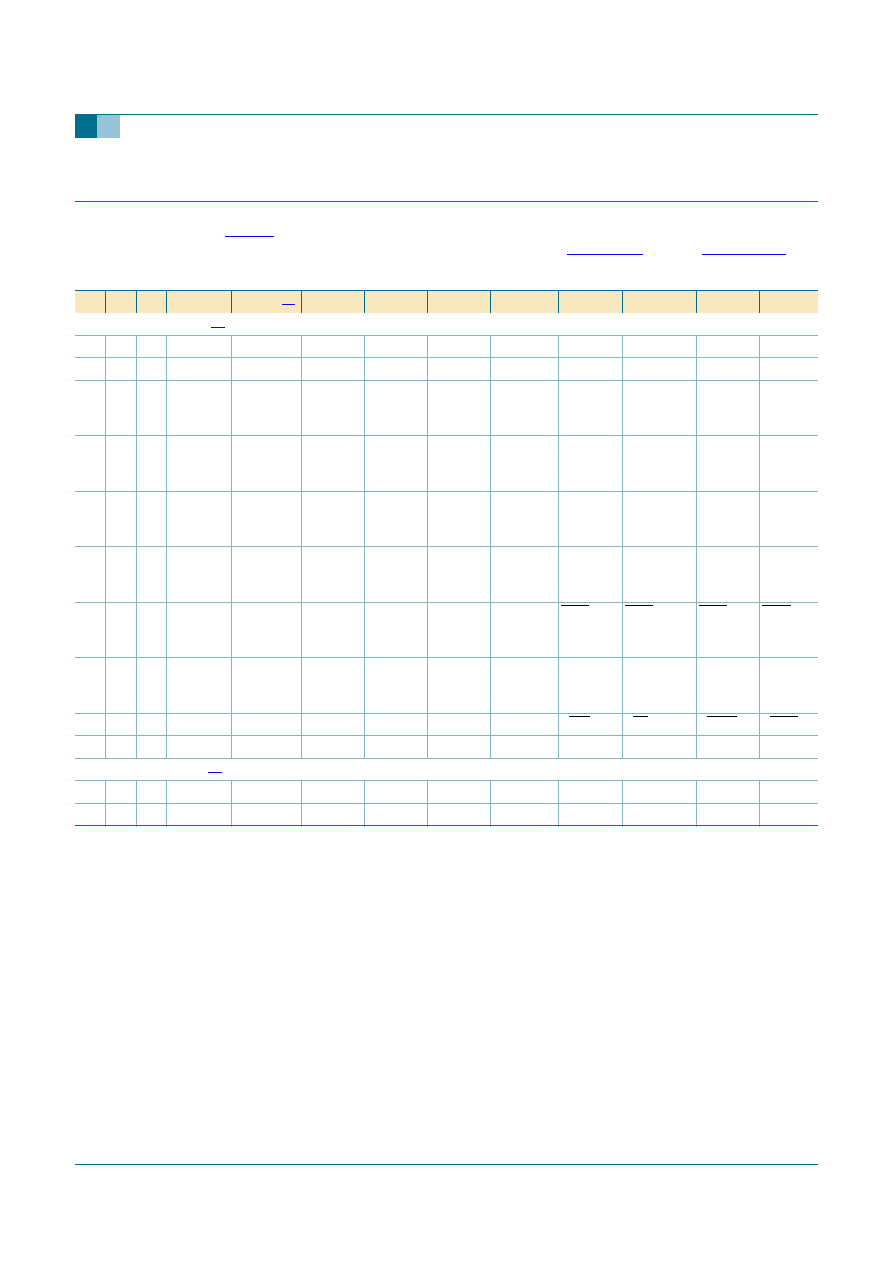
Table 3:
Serial port channel selection, 16 mode interface
CSA
CSB
CSC
CSD
UART channel
1
1
1
1
none
0
1
1
1
A
1
0
1
1
B
1
1
0
1
C
1
1
1
0
D
Table 4:
Serial port channel selection, 68 mode interface
CS
A4
A3
UART channel
1
n/a
n/a
none
0
0
0
A
0
0
1
B
0
1
0
C
0
1
1
D

9397 750 13133
© Koninklijke Philips Electronics N.V. 2005. All rights reserved.
Product data sheet
Rev. 01 -- 9 February 2005
15 of 51
Philips Semiconductors
SC16C554B/554DB
5 V, 3.3 V and 2.5 V quad UART, 5 Mbit/s (max.) with 16-byte FIFOs
6.2 Internal registers
The SC16C554B/554DB provides 12 internal registers for monitoring and control. These
registers are shown in
Table 5
. These registers function as data holding registers
(THR/RHR), interrupt status and control registers (IER/ISR), a FIFO control register
(FCR), line status and control registers (LCR/LSR), modem status and control registers
(MCR/MSR), programmable data rate (clock) control registers (DLL/DLM), and a user
accessible scratchpad register (SPR). Register functions are more fully described in the
following paragraphs.
[1]
These registers are accessible only when LCR[7] is a logic 0.
[2]
These registers are accessible only when LCR[7] is a logic 1.
6.3 FIFO operation
The 16 byte transmit and receive data FIFOs are enabled by the FIFO Control Register
(FCR) bit 0. With SC16C554B devices, the user can set the receive trigger level, but not
the transmit trigger level. The receiver FIFO section includes a time-out function to ensure
data is delivered to the external CPU. An interrupt is generated whenever the Receive
Holding Register (RHR) has not been read following the loading of a character or the
receive trigger level has not been reached.
Table 5:
Internal registers decoding
A2
A1
A0
Read mode
Write mode
General register set (THR/RHR, IER/ISR, MCR/MSR, FCR, LSR, SPR)
[1]
0
0
0
Receive Holding Register
Transmit Holding Register
0
0
1
Interrupt Enable Register
Interrupt Enable Register
0
1
0
Interrupt Status Register
FIFO Control Register
0
1
1
Line Control Register
Line Control Register
1
0
0
Modem Control Register
Modem Control Register
1
0
1
Line Status Register
n/a
1
1
0
Modem Status Register
n/a
1
1
1
Scratchpad Register
Scratchpad Register
Baud rate register set (DLL/DLM)
[2]
0
0
0
LSB of Divisor Latch
LSB of Divisor Latch
0
0
1
MSB of Divisor Latch
MSB of Divisor Latch
Table 6:
Flow control mechanism
Selected trigger level
(characters)
INT pin activation
Negate RTS
Assert RTS
1
1
4
1
4
4
8
4
8
8
12
8
14
14
14
10
9397 750 13133
© Koninklijke Philips Electronics N.V. 2005. All rights reserved.
Product data sheet
Rev. 01 -- 9 February 2005
16 of 51
Philips Semiconductors
SC16C554B/554DB
5 V, 3.3 V and 2.5 V quad UART, 5 Mbit/s (max.) with 16-byte FIFOs
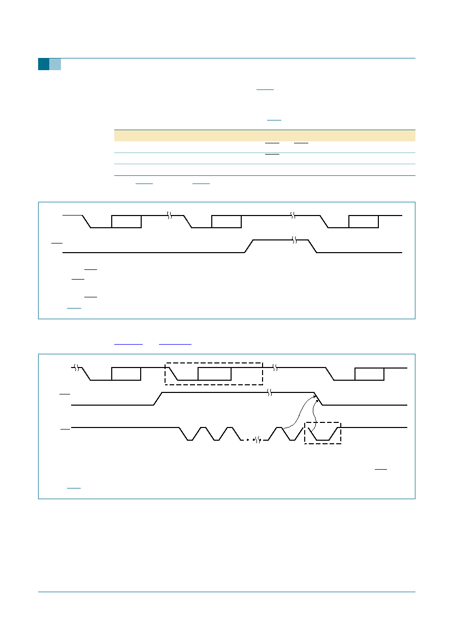
6.4 Autoflow control (see
Figure 7
)
Autoflow control is comprised of auto-CTS and auto-RTS. With auto-CTS, the CTS input
must be active before the transmitter FIFO can emit data. With auto-RTS, RTS becomes
active when the receiver needs more data and notifies the sending serial device. When
RTS is connected to CTS, data transmission does not occur unless the receiver FIFO has
space for the data; thus, overrun errors are eliminated using UART 1 and UART 2 from a
SC16C554B/554DB with the autoflow control enabled. If not, overrun errors occur when
the transmit data rate exceeds the receiver FIFO read latency.
6.4.1 Auto-RTS (see
Figure 7
)
Auto-RTS data flow control originates in the receiver timing and control block (see block
diagrams in
Figure 1
and
Figure 2
) and is linked to the programmed receiver FIFO trigger
level. When the receiver FIFO level reaches a trigger level of 1, 4, or 8 (see
Figure 9
), RTS
is de-asserted. With trigger levels of 1, 4, and 8, the sending UART may send an
additional byte after the trigger level is reached (assuming the sending UART has another
byte to send) because it may not recognize the de-assertion of RTS until after it has
begun sending the additional byte. RTS is automatically reasserted once the RX FIFO is
emptied by reading the receiver buffer register. When the trigger level is 14 (see
Figure 10
), RTS is de-asserted after the first data bit of the 16th character is present on
the RX line. RTS is reasserted when the RX FIFO has at least one available byte space.
6.4.2 Auto-CTS (see
Figure 7
)
The transmitter circuitry checks CTS before sending the next data byte. When CTS is
active, it sends the next byte. To stop the transmitter from sending the following byte, CTS
must be released before the middle of the last stop bit that is currently being sent (see
Figure 8
). The auto-CTS function reduces interrupts to the host system. When flow control
is enabled, CTS level changes do not trigger host interrupts because the device
automatically controls its own transmitter. Without auto-CTS, the transmitter sends any
data present in the transmit FIFO and a receiver overrun error may result.
Fig 7.
Autoflow control (auto-RTS and auto-CTS) example
RCV
FIFO
SERIAL TO
PARALLEL
FLOW
CONTROL
XMT
FIFO
PARALLEL
TO SERIAL
FLOW
CONTROL
PARALLEL
TO SERIAL
FLOW
CONTROL
SERIAL TO
PARALLEL
FLOW
XMT
FIFO
RCV
FIFO
ACE1
ACE2
D7 to D0
RX
TX
RTS
CTS
TX
RX
D7 to D0
CONTROL
002aaa048
CTS
RTS
9397 750 13133
© Koninklijke Philips Electronics N.V. 2005. All rights reserved.
Product data sheet
Rev. 01 -- 9 February 2005
17 of 51
Philips Semiconductors
SC16C554B/554DB
5 V, 3.3 V and 2.5 V quad UART, 5 Mbit/s (max.) with 16-byte FIFOs
6.4.3 Enabling autoflow control and auto-CTS
Autoflow control is enabled by setting MCR[5] and MCR[1].
6.4.4 Auto-CTS and auto-RTS functional timing
The receiver FIFO trigger level can be set to 1, 4, 8, or 14 bytes. These are described in
Figure 9
and
Figure 10
.
Table 7:
Enabling autoflow control and auto-CTS
MCR[5]
MCR[1]
Selection
1
1
auto RTS and CTS
1
0
auto CTS
0
X
disable
(1) When CTS is LOW, the transmitter keeps sending serial data out.
(2) If CTS goes HIGH before the middle of the last stop bit of the current byte, the transmitter finishes sending the current byte,
but is does not send the next byte.
(3) When CTS goes from HIGH to LOW, the transmitter begins sending data again.
Fig 8.
CTS functional timing waveforms
Start
bits 0 to 7
Stop
TX
CTS
002aaa049
Start
bits 0 to 7
Stop
Start
bits 0 to 7
Stop
(1) N = RCV FIFO trigger level (1, 4, or 8 bytes).
(2) The two blocks in dashed lines cover the case where an additional byte is sent as described in the preceding auto-RTS
section.
Fig 9.
RTS functional timing waveforms, RCV FIFO trigger level = 1, 4, or 8 bytes
Start
byte N
Start
byte N + 1
Start
byte
Stop
Stop
Stop
RX
RTS
IOR
(RD RBR)
N
N + 1
1
2
002aaa050
9397 750 13133
© Koninklijke Philips Electronics N.V. 2005. All rights reserved.
Product data sheet
Rev. 01 -- 9 February 2005
18 of 51
Philips Semiconductors
SC16C554B/554DB
5 V, 3.3 V and 2.5 V quad UART, 5 Mbit/s (max.) with 16-byte FIFOs
6.5 Hardware/software and time-out interrupts
Following a reset, if the transmitter interrupt is enabled, the SC16C554B/554DB will issue
an interrupt to indicate that the Transmit Holding Register is empty. This interrupt must be
serviced prior to continuing operations. The LSR register provides the current singular
highest priority interrupt only. Only after servicing the higher pending interrupt will the
lower priority interrupt(s) be reflected in the status register. Servicing the interrupt without
investigating further interrupt conditions can result in data errors.
When two interrupt conditions have the same priority, it is important to service these
interrupts correctly. Receive Data Ready and Receive Time Out have the same interrupt
priority (when enabled by IER[0]). The receiver issues an interrupt after the number of
characters have reached the programmed trigger level. In this case, the
SC16C554B/554DB FIFO may hold more characters than the programmed trigger level.
Following the removal of a data byte, the user should re-check LSR[0] for additional
characters. A Receive Time Out will not occur if the receive FIFO is empty. The time-out
counter is reset at the center of each stop bit received or each time the receive holding
register (RHR) is read. The actual time-out value is 4 character time.
In the 16 mode for the PLCC68 package, the system/board designer can optionally
provide software controlled 3-state interrupt operation. This is accomplished by INTSEL
and MCR[3]. When INTSEL interface pin is left open or made a logic 0, MCR[3] controls
the 3-state interrupt outputs, INTA to INTD. When INTSEL is a logic 1, MCR[3] has no
effect on the INTA to INTD outputs, and the package operates with interrupt outputs
enabled continuously.
6.6 Programmable baud rate generator
The SC16C554B/554DB supports high speed modem technologies that have increased
input data rates by employing data compression schemes. For example, a 33.6 kbit/s
modem that employs data compression may require a 115.2 kbit/s input data rate.
A 128.0 kbit/s ISDN modem that supports data compression may need an input data rate
of 460.8 kbit/s.
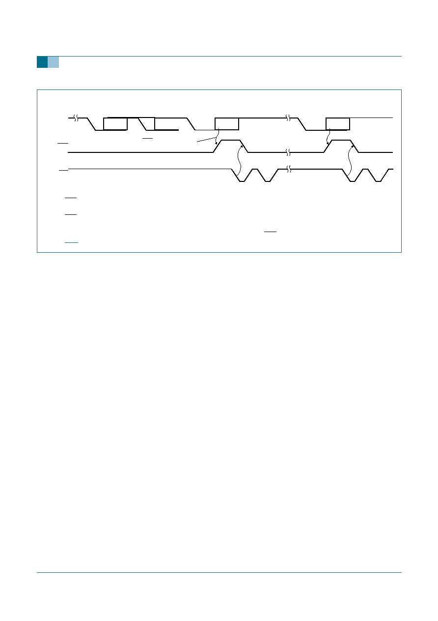
(1) RTS is de-asserted when the receiver receives the first data bit of the sixteenth byte. The receive FIFO is full after finishing
the sixteenth byte.
(2) RTS is asserted again when there is at least one byte of space available and no incoming byte is in processing, or there is
more than one byte of space available.
(3) When the receive FIFO is full, the first receive buffer register read re-asserts RTS.
Fig 10. RTS functional timing waveforms, RCV FIFO trigger level = 14 bytes
byte 14
byte 15
RX
RTS
IOR
(RD RBR)
Start
byte 18
Stop
Start
byte 16
Stop
002aaa051
RTS released after the
first data bit of byte 16
9397 750 13133
© Koninklijke Philips Electronics N.V. 2005. All rights reserved.
Product data sheet
Rev. 01 -- 9 February 2005
19 of 51
Philips Semiconductors
SC16C554B/554DB
5 V, 3.3 V and 2.5 V quad UART, 5 Mbit/s (max.) with 16-byte FIFOs
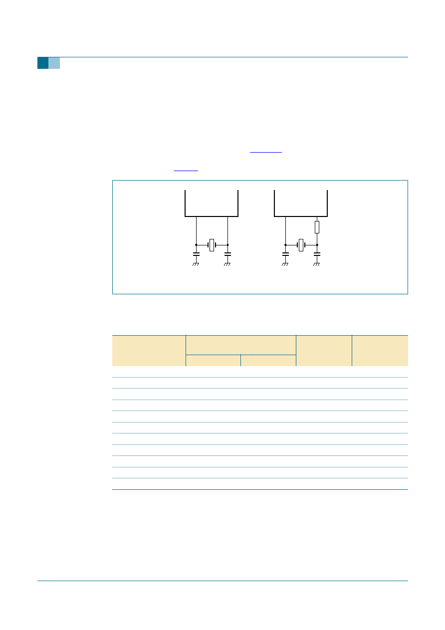
A single baud rate generator is provided for the transmitter and receiver, allowing
independent TX/RX channel control. The programmable Baud Rate Generator is capable
of accepting an input clock up to 80 MHz (for 3.3 V and 5 V operation), as required for
supporting a 5 Mbit/s data rate. The SC16C554B/554DB can be configured for internal or
external clock operation. For internal clock oscillator operation, an industry standard
microprocessor crystal (parallel resonant/22 pF to 33 pF load) is connected externally
between the XTAL1 and XTAL2 pins (see
Figure 11
). Alternatively, an external clock can
be connected to the XTAL1 pin to clock the internal baud rate generator for standard or
custom rates (see
Table 8
).
Programming the Baud Rate Generator registers DLM (MSB) and DLL (LSB) provides a
user capability for selecting the desired final baud rate.
Fig 11. Crystal oscillator connection
Table 8:
Baud rate generator programming table using a 7.3728 MHz clock
Output baud rate
User
16
◊
clock divisor
DLM
program value
(HEX)
DLL
program value
(HEX)
Decimal
HEX
200
2304
900
09
00
1200
384
180
01
80
2400
192
C0
00
C0
4800
96
60
00
60
9600
48
30
00
30
19.2 k
24
18
00
18
38.4 k
12
0C
00
0C
76.8 k
6
06
00
06
153.6 k
3
03
00
03
230.4 k
2
02
00
02
460.8 k
1
01
00
01
002aaa870
C2
47 pF
XTAL1
XTAL2
X1
1.8432 MHz
C1
22 pF
C2
33 pF
XTAL1
XTAL2
1.5 k
X1
1.8432 MHz
C1
22 pF

9397 750 13133
© Koninklijke Philips Electronics N.V. 2005. All rights reserved.
Product data sheet
Rev. 01 -- 9 February 2005
20 of 51
Philips Semiconductors
SC16C554B/554DB
5 V, 3.3 V and 2.5 V quad UART, 5 Mbit/s (max.) with 16-byte FIFOs
6.7 DMA operation
The SC16C554B/554DB FIFO trigger level provides additional flexibility to the user for
block mode operation. LSR[5:6] provide an indication when the transmitter is empty or has
an empty location(s). The user can optionally operate the transmit and receive FIFOs in
the DMA mode (FCR[3]). When the transmit and receive FIFOs are enabled and the DMA
mode is de-activated (DMA Mode 0), the SC16C554B/554DB activates the interrupt
output pin for each data transmit or receive operation. When DMA mode is activated
(DMA Mode 1), the user takes the advantage of block mode operation by loading or
unloading the FIFO in a block sequence determined by the preset trigger level. In this
mode, the SC16C554B/554DB sets the interrupt output pin when the characters in the
receive FIFOs are above the receive trigger level.
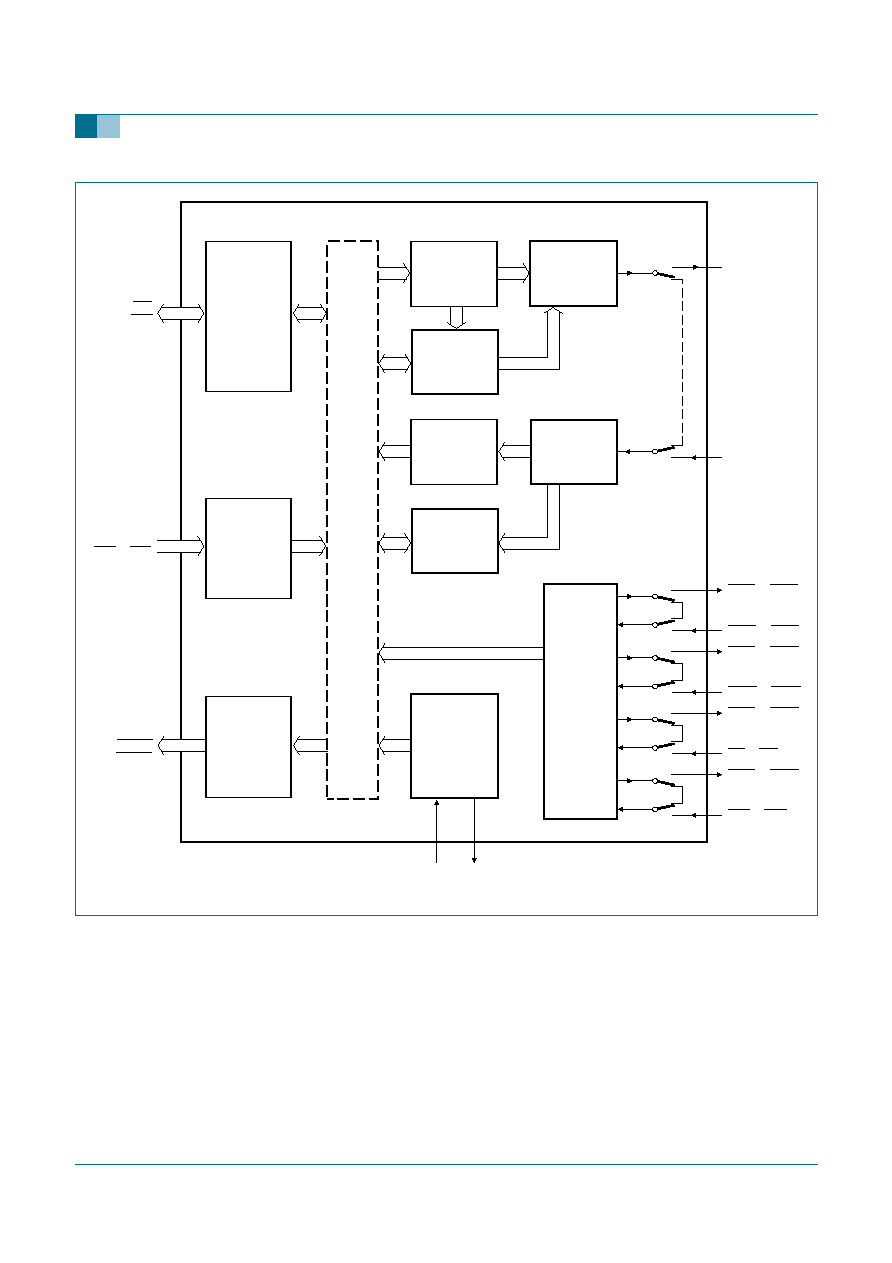
6.8 Loop-back mode
The internal loop-back capability allows on-board diagnostics. In the loop-back mode, the
normal modem interface pins are disconnected and reconfigured for loop-back internally.
MCR[0:3] register bits are used for controlling loop-back diagnostic testing. In the
loop-back mode, OP1 and OP2 in the MCR register (bits 2:3) control the modem RI and
CD inputs, respectively. MCR signals DTR and RTS (bits 0:1) are used to control the
modem DSR and CTS inputs, respectively. The transmitter output (TX) and the receiver
input (RX) are disconnected from their associated interface pins, and instead are
connected together internally (see
Figure 12
). The CTS, DSR, CD, and RI are
disconnected from their normal modem control input pins, and instead are connected
internally to RTS, DTR, OP2 and OP1. Loop-back test data is entered into the transmit
holding register via the user data bus interface, D0 to D7. The transmit UART serializes
the data and passes the serial data to the receive UART via the internal loop-back
connection. The receive UART converts the serial data back into parallel data that is then
made available at the user data interface D0 to D7. The user optionally compares the
received data to the initial transmitted data for verifying error-free operation of the UART
TX/RX circuits.
In this mode, the receiver and transmitter interrupts are fully operational. The Modem
Control Interrupts are also operational. However, the interrupts can only be read using
lower four bits of the Modem Status Register (MSR[0:3]) instead of the four Modem Status
Register bits 4:7. The interrupts are still controlled by the IER.
9397 750 13133
© Koninklijke Philips Electronics N.V. 2005. All rights reserved.
Product data sheet
Rev. 01 -- 9 February 2005
21 of 51
Philips Semiconductors
SC16C554B/554DB
5 V, 3.3 V and 2.5 V quad UART, 5 Mbit/s (max.) with 16-byte FIFOs
Fig 12. Internal loop-back mode diagram (16 mode)
CTSA to CTSD
TRANSMIT
FIFO
REGISTERS
TXA to TXD
RECEIVE
SHIFT
REGISTER
RECEIVE
FIFO
REGISTERS
RXA to RXD
INTERCONNECT B
US LINES
AND
CONTR
OL SIGNALS
SC16C554B/554DB
TRANSMIT
SHIFT
REGISTER
XTAL2
XTAL1
002aaa883
FLOW
CONTROL
LOGIC
DATA BUS
AND
CONTROL
LOGIC
REGISTER
SELECT
LOGIC
INTERRUPT
CONTROL
LOGIC
D0 to D7
IOR
IOW
RESET
A0 to A2
CSA to CSD
INTA to INTD
TXRDY
RXRDY
CLOCK AND
BAUD RATE
GENERATOR
MODEM
CONTROL
LOGIC
FLOW
CONTROL
LOGIC
RTSA to RTSD
DSRA to DSRD
DTRA to DTRD
RIA to RID
OP1A to OP1D
CDA to CDD
OP2A to OP2D
MCR[4] = 1
Philips Semiconductors
SC16C554B/554DB
5 V, 3.3 V and 2.5 V quad UART, 5 Mbit/s (max.) with 16-byte FIFOs
9397 750 13133
© Koninklijke Philips Electronics N.V. 2005. All rights reserved.
Product data sheet
Rev. 01 -- 9 February 2005
22 of 51
Fig 13. Internal loop-back mode diagram (68 mode)
CTSA to CTSD
TRANSMIT
FIFO
REGISTERS
TXA to TXD
RECEIVE
SHIFT
REGISTER
RECEIVE
FIFO
REGISTERS
RXA to RXD
INTERCONNECT B
US LINES
AND
CONTR
OL SIGNALS
SC16C554B/554DB
TRANSMIT
SHIFT
REGISTER
XTAL2
XTAL1
002aaa884
FLOW
CONTROL
LOGIC
DATA BUS
AND
CONTROL
LOGIC
REGISTER
SELECT
LOGIC
INTERRUPT
CONTROL
LOGIC
D0 to D7
R/W
RESET
A0 to A4
CS
IRQ
TXRDY
RXRDY
CLOCK AND
BAUD RATE
GENERATOR
MODEM
CONTROL
LOGIC
FLOW
CONTROL
LOGIC
RTSA to RTSD
DSRA to DSRD
DTRA to DTRD
RIA to RID
OP1A to OP1D
CDA to CDD
OP2A to OP2D
MCR[4] = 1
16/68
9397 750 13133
© Koninklijke Philips Electronics N.V. 2005. All rights reserved.
Product data sheet
Rev. 01 -- 9 February 2005
23 of 51
Philips Semiconductors
SC16C554B/554DB
5 V, 3.3 V and 2.5 V quad UART, 5 Mbit/s (max.) with 16-byte FIFOs
7.
Register descriptions
Table 9
details the assigned bit functions for the SC16C554B/554DB internal registers.
The assigned bit functions are more fully defined in
Section 7.1
through
Section 7.10
.
[1]
The value shown represents the register's initialized HEX value; X = not applicable.
[2]
These registers are accessible only when LCR[7] = 0.
[3]
The Special Register set is accessible only when LCR[7] is set to a logic 1.
Table 9:
SC16C554B/554DB internal registers
A2
A1
A0
Register Default
[1]
Bit 7
Bit 6
Bit 5
Bit 4
Bit 3
Bit 2
Bit 1
Bit 0
General Register set
[2]
0
0
0
RHR
XX
bit 7
bit 6
bit 5
bit 4
bit 3
bit 2
bit 1
bit 0
0
0
0
THR
XX
bit 7
bit 6
bit 5
bit 4
bit 3
bit 2
bit 1
bit 0
0
0
1
IER
00
0
0
0
0
modem
status
interrupt
receive
line status
interrupt
transmit
holding
register
receive
holding
register
0
1
0
FCR
00
RCVR
trigger
(MSB)
RCVR
trigger
(LSB)
reserved reserved
DMA
mode
select
XMIT
FIFO reset
RCVR
FIFO
reset
FIFO
enable
0
1
0
ISR
01
FIFOs
enabled
FIFOs
enabled
0
0
INT
priority
bit 2
INT
priority
bit 1
INT
priority
bit 0
INT
status
0
1
1
LCR
00
divisor
latch
enable
set
break
set
parity
even
parity
parity
enable
stop bits
word
length
bit 1
word
length
bit 0
1
0
0
MCR
00
0
0
autoflow
control
enable
loop back OP2,
INTx
enable
OP1
RTS
DTR
1
0
1
LSR
60
FIFO
data
error
trans.
empty
trans.
holding
empty
break
interrupt
framing
error
parity
error
overrun
error
receive
data
ready
1
1
0
MSR
X0
CD
RI
DSR
CTS
CD
RI
DSR
CTS
1
1
1
SPR
FF
bit 7
bit 6
bit 5
bit 4
bit 3
bit 2
bit 1
bit 0
Special Register set
[3]
0
0
0
DLL
XX
bit 7
bit 6
bit 5
bit 4
bit 3
bit 2
bit 1
bit 0
0
0
1
DLM
XX
bit 15
bit 14
bit 13
bit 12
bit 11
bit 10
bit 9
bit 8

9397 750 13133
© Koninklijke Philips Electronics N.V. 2005. All rights reserved.
Product data sheet
Rev. 01 -- 9 February 2005
24 of 51
Philips Semiconductors
SC16C554B/554DB
5 V, 3.3 V and 2.5 V quad UART, 5 Mbit/s (max.) with 16-byte FIFOs
7.1 Transmit (THR) and Receive (RHR) Holding Registers
The serial transmitter section consists of an 8-bit Transmit Hold Register (THR) and
Transmit Shift Register (TSR). The status of the THR is provided in the Line Status
Register (LSR). Writing to the THR transfers the contents of the data bus (D7 to D0) to the
THR, providing that the THR or TSR is empty. The THR empty flag in the LSR register will
be set to a logic 1 when the transmitter is empty or when data is transferred to the TSR.
Note that a write operation can be performed when the THR empty flag is set
(logic 0 = FIFO full; logic 1 = at least one FIFO location available).
The serial receive section also contains an 8-bit Receive Holding Register (RHR).
Receive data is removed from the SC16C554B/554DB and receive FIFO by reading the
RHR register. The receive section provides a mechanism to prevent false starts. On the
falling edge of a start or false start bit, an internal receiver counter starts counting clocks
at the 16
◊
clock rate. After 7
1
/
2
clocks, the start bit time should be shifted to the center of
the start bit. At this time the start bit is sampled, and if it is still a logic 0 it is validated.
Evaluating the start bit in this manner prevents the receiver from assembling a false
character. Receiver status codes will be posted in the LSR.
7.2 Interrupt Enable Register (IER)
The Interrupt Enable Register (IER) masks the interrupts from receiver ready, transmitter
empty, line status and modem status registers. These interrupts would normally be seen
on the INTA to INTD output pins in the 16 mode, or on wire-OR IRQ output pin in the
68 mode.
Table 10:
Interrupt Enable Register bits description
Bit
Symbol
Description
7:4
IER[7:4]
Reserved; set to `0'.
3
IER[3]
Modem Status Interrupt.
Logic 0 = Disable the modem status register interrupt (normal default
condition).
Logic 1 = Enable the modem status register interrupt.
2
IER[2]
Receive Line Status interrupt.
Logic 0 = Disable the receiver line status interrupt (normal default condition).
Logic 1 = Enable the receiver line status interrupt.
1
IER[1]
Transmit Holding Register interrupt. This interrupt will be issued whenever the
THR is empty, and is associated with LSR[1].
Logic 0 = Disable the transmitter empty interrupt (normal default condition).
Logic 1 = Enable the transmitter empty interrupt.
0
IER[0]
Receive Holding Register interrupt. This interrupt will be issued when the FIFO
has reached the programmed trigger level, or is cleared when the FIFO drops
below the trigger level in the FIFO mode of operation.
Logic 0 = Disable the receiver ready interrupt (normal default condition).
Logic 1 = Enable the receiver ready interrupt.

9397 750 13133
© Koninklijke Philips Electronics N.V. 2005. All rights reserved.
Product data sheet
Rev. 01 -- 9 February 2005
25 of 51
Philips Semiconductors
SC16C554B/554DB
5 V, 3.3 V and 2.5 V quad UART, 5 Mbit/s (max.) with 16-byte FIFOs
7.2.1 IER versus Receive FIFO interrupt mode operation
When the receive FIFO (FCR[0] = logic 1), and receive interrupts (IER[0] = logic 1) are
enabled, the receive interrupts and register status will reflect the following:
∑
The receive data available interrupts are issued to the external CPU when the FIFO
has reached the programmed trigger level. It will be cleared when the FIFO drops
below the programmed trigger level.
∑
FIFO status will also be reflected in the user accessible ISR register when the FIFO
trigger level is reached. Both the ISR register status bit and the interrupt will be
cleared when the FIFO drops below the trigger level.
∑
The data ready bit (LSR[0]) is set as soon as a character is transferred from the shift
register to the receive FIFO. It is reset when the FIFO is empty.
7.2.2 IER versus Receive/Transmit FIFO polled mode operation
When FCR[0] = logic 1, resetting IER[0:3] enables the SC16C554B/554DB in the FIFO
polled mode of operation. Since the receiver and transmitter have separate bits in the
LSR, either or both can be used in the polled mode by selecting respective transmit or
receive control bit(s).
∑
LSR[0] will be a logic 1 as long as there is one byte in the receive FIFO.
∑
LSR[1:4] will provide the type of errors encountered, if any.
∑
LSR[5] will indicate when the transmit FIFO is empty.
∑
LSR[6] will indicate when both the transmit FIFO and transmit shift register are empty.
∑
LSR[7] will indicate any FIFO data errors.
7.3 FIFO Control Register (FCR)
This register is used to enable the FIFOs, clear the FIFOs, set the receive FIFO trigger
levels, and select the DMA mode.
7.3.1 DMA mode
7.3.1.1
Mode 0 (FCR bit 3 = 0)
Set and enable the interrupt for each single transmit or receive operation, and is similar to
the 16C454 mode. Transmit Ready (TXRDY) will go to a logic 0 whenever an empty
transmit space is available in the Transmit Holding Register (THR). Receive Ready
(RXRDY) will go to a logic 0 whenever the Receive Holding Register (RHR) is loaded with
a character.
7.3.1.2
Mode 1 (FCR bit 3 = 1)
Set and enable the interrupt in a block mode operation. The transmit interrupt is set when
there are one or more FIFO locations empty. The receive interrupt is set when the receive
FIFO fills to the programmed trigger level. However, the FIFO continues to fill regardless
of the programmed level until the FIFO is full. RXRDY remains a logic 0 as long as the
FIFO fill level is above the programmed trigger level.

9397 750 13133
© Koninklijke Philips Electronics N.V. 2005. All rights reserved.
Product data sheet
Rev. 01 -- 9 February 2005
26 of 51
Philips Semiconductors
SC16C554B/554DB
5 V, 3.3 V and 2.5 V quad UART, 5 Mbit/s (max.) with 16-byte FIFOs
7.3.2 FIFO mode
Table 11:
FIFO Control Register bits description
Bit
Symbol
Description
7:6
FCR[7:6]
RCVR trigger. These bits are used to set the trigger level for the receive
FIFO interrupt.
An interrupt is generated when the number of characters in the FIFO equals
the programmed trigger level. However, the FIFO will continue to be loaded
until it is full. Refer to
Table 12
.
5:4
FCR[5:4]
Not used; initialized to logic 0.
3
FCR[3]
DMA mode select.
Logic 0 = Set DMA mode `0' (normal default condition).
Logic 1 = Set DMA mode `1'
Transmit operation in mode `0': When the SC16C554B/554DB is in the
16C450 mode (FIFOs disabled; FCR[0] = logic 0) or in the FIFO mode
(FIFOs enabled; FCR[0] = logic 1; FCR[3] = logic 0), and when there are no
characters in the transmit FIFO or transmit holding register, the TXRDY pin
will be a logic 0. Once active, the TXRDY pin will go to a logic 1 after the first
character is loaded into the transmit holding register.
Receive operation in mode `0': When the SC16C554B/554DB is in
mode `0' (FCR[0] = logic 0), or in the FIFO mode (FCR[0] = logic 1; FCR[3] =
logic 0) and there is at least one character in the receive FIFO, the RXRDY
pin will be a logic 0. Once active, the RXRDY pin will go to a logic 1 when
there are no more characters in the receiver.
Transmit operation in mode `1': When the SC16C554B/554DB is in FIFO
mode (FCR[0] = logic 1; FCR[3] = logic 1), the TXRDY pin will be a logic 1
when the transmit FIFO is completely full. It will be a logic 0 if one or more
FIFO locations are empty.
Receive operation in mode `1': When the SC16C554B/554DB is in FIFO
mode (FCR[0] = logic 1; FCR[3] = logic 1) and the trigger level has been
reached, or a Receive Time-out has occurred, the RXRDY pin will go to a
logic 0. Once activated, it will go to a logic 1 after there are no more
characters in the FIFO.
2
FCR[2]
XMIT FIFO reset.
Logic 0 = No FIFO transmit reset (normal default condition).
Logic 1 = Clears the contents of the transmit FIFO and resets the FIFO
counter logic (the transmit shift register is not cleared or altered). This bit
will return to a logic 0 after clearing the FIFO.
1
FCR[1]
RCVR FIFO reset.
Logic 0 = No FIFO receive reset (normal default condition).
Logic 1 = Clears the contents of the receive FIFO and resets the FIFO
counter logic (the receive shift register is not cleared or altered). This bit
will return to a logic 0 after clearing the FIFO.
0
FCR[0]
FIFO enable.
Logic 0 = Disable the transmit and receive FIFO (normal default
condition).
Logic 1 = Enable the transmit and receive FIFO. This bit must be a `1'
when other FCR bits are written to, or they will not be programmed.

9397 750 13133
© Koninklijke Philips Electronics N.V. 2005. All rights reserved.
Product data sheet
Rev. 01 -- 9 February 2005
27 of 51
Philips Semiconductors
SC16C554B/554DB
5 V, 3.3 V and 2.5 V quad UART, 5 Mbit/s (max.) with 16-byte FIFOs
7.4 Interrupt Status Register (ISR)
The SC16C554B/554DB provides four levels of prioritized interrupts to minimize external
software interaction. The Interrupt Status Register (ISR) provides the user with four
interrupt status bits. Performing a read cycle on the ISR will provide the user with the
highest pending interrupt level to be serviced. No other interrupts are acknowledged until
the pending interrupt is serviced. Whenever the interrupt status register is read, the
interrupt status is cleared. However, it should be noted that only the current pending
interrupt is cleared by the read. A lower level interrupt may be seen after re-reading the
interrupt status bits.
Table 13 "Interrupt source"
shows the data values (bits 0 to 5) for the
four prioritized interrupt levels and the interrupt sources associated with each of these
interrupt levels.
Table 12:
RCVR trigger levels
FCR[7]
FCR[6]
RX FIFO trigger level
0
0
1
0
1
4
1
0
8
1
1
14
Table 13:
Interrupt source
Priority
level
ISR[5]
ISR[4]
ISR[3]
ISR[2]
ISR[1]
ISR[0]
Source of the interrupt
1
0
0
0
1
1
0
LSR (Receiver Line Status
Register)
2
0
0
0
1
0
0
RXRDY (Receive Data
Ready)
2
0
0
1
1
0
0
RXRDY (Receive Data
time-out)
3
0
0
0
0
1
0
TXRDY (Transmitter Holding
Register Empty)
4
0
0
0
0
0
0
MSR (Modem Status
Register)
Table 14:
Interrupt Status Register bits description
Bit
Symbol
Description
7:6
ISR[7:6]
FIFOs enabled. These bits are set to a logic 0 when the FIFO is not
being used. They are set to a logic 1 when the FIFOs are enabled.
Logic 0 or cleared = default condition.
5:4
ISR[5:4]
Reserved; set to `0'.
3:1
ISR[3:1]
INT priority bits 2 to 0. These bits indicate the source for a pending
interrupt at interrupt priority levels 1, 2, and 3 (see
Table 13
).
Logic 0 or cleared = default condition.
0
ISR[0]
INT status.
Logic 0 = An interrupt is pending and the ISR contents may be used
as a pointer to the appropriate interrupt service routine.
Logic 1 = No interrupt pending (normal default condition).

9397 750 13133
© Koninklijke Philips Electronics N.V. 2005. All rights reserved.
Product data sheet
Rev. 01 -- 9 February 2005
28 of 51
Philips Semiconductors
SC16C554B/554DB
5 V, 3.3 V and 2.5 V quad UART, 5 Mbit/s (max.) with 16-byte FIFOs
7.5 Line Control Register (LCR)
The Line Control Register is used to specify the asynchronous data communication
format. The word length, the number of stop bits, and the parity are selected by writing the
appropriate bits in this register.
Table 15:
Line Control Register bits description
Bit
Symbol
Description
7
LCR[7]
Divisor latch enable. The internal baud rate counter latch and
Enhance Feature mode enable.
Logic 0 = Divisor latch disabled (normal default condition).
Logic 1 = Divisor latch enabled.
6
LCR[6]
Set break. When enabled, the Break control bit causes a break
condition to be transmitted (the TX output is forced to a logic 0 state).
This condition exists until disabled by setting LCR[6] to a logic 0.
Logic 0 = no TX break condition (normal default condition).
Logic 1 = forces the transmitter output (TX) to a logic 0 for alerting
the remote receiver to a line break condition.
5
LCR[5]
Set parity. If the parity bit is enabled, LCR[5] selects the forced parity
format. Programs the parity conditions (see
Table 16
).
Logic 0 = parity is not forced (normal default condition).
LCR[5] = logic 1 and LCR[4] = logic 0: parity bit is forced to a
logical 1 for the transmit and receive data.
LCR[5] = logic 1 and LCR[4] = logic 1: parity bit is forced to a
logical 0 for the transmit and receive data.
4
LCR[4]
Even parity. If the parity bit is enabled with LCR[3] set to a logic 1,
LCR[4] selects the even or odd parity format.
Logic 0 = Odd Parity is generated by forcing an odd number of
logic 1s in the transmitted data. The receiver must be programmed
to check the same format (normal default condition).
Logic 1 = Even Parity is generated by forcing an even number of
logic 1s in the transmitted data. The receiver must be programmed
to check the same format.
3
LCR[3]
Parity enable. Parity or no parity can be selected via this bit.
Logic 0 = no parity (normal default condition).
Logic 1 = a parity bit is generated during the transmission, receiver
checks the data and parity for transmission errors.
2
LCR[2]
Stop bits. The length of stop bit is specified by this bit in conjunction
with the programmed word length (see
Table 17
).
Logic 0 or cleared = default condition.
1:0
LCR[1:0]
Word length bits 1, 0. These two bits specify the word length to be
transmitted or received (see
Table 18
).
Logic 0 or cleared = default condition.

9397 750 13133
© Koninklijke Philips Electronics N.V. 2005. All rights reserved.
Product data sheet
Rev. 01 -- 9 February 2005
29 of 51
Philips Semiconductors
SC16C554B/554DB
5 V, 3.3 V and 2.5 V quad UART, 5 Mbit/s (max.) with 16-byte FIFOs
Table 16:
LCR[5] parity selection
LCR[5]
LCR[4]
LCR[3]
Parity selection
X
X
0
no parity
0
0
1
odd parity
0
1
1
even parity
1
0
1
forced parity `1'
1
1
1
forced parity `0'
Table 17:
LCR[2] stop bit length
LCR[2]
Word length
Stop bit length (bit times)
0
5, 6, 7, 8
1
1
5
1
1
/
2
1
6, 7, 8
2
Table 18:
LCR[1:0] word length
LCR[1]
LCR[0]
Word length
0
0
5
0
1
6
1
0
7
1
1
8

9397 750 13133
© Koninklijke Philips Electronics N.V. 2005. All rights reserved.
Product data sheet
Rev. 01 -- 9 February 2005
30 of 51
Philips Semiconductors
SC16C554B/554DB
5 V, 3.3 V and 2.5 V quad UART, 5 Mbit/s (max.) with 16-byte FIFOs
7.6 Modem Control Register (MCR)
This register controls the interface with the modem or a peripheral device.
Table 19:
Modem Control Register bits description
Bit
Symbol
Description
7:6
MCR[7:6]
Reserved; set to `0'.
5
MCR[5]
Autoflow control enable.
4
MCR[4]
Loop-back. Enable the local loop-back mode (diagnostics). In this mode
the transmitter output (TX) and the receiver input (RX), CTS, DSR, CD,
and RI are disconnected from the SC16C554B/554DB I/O pins. Internally
the modem data and control pins are connected into a loop-back data
configuration (see
Figure 12
). In this mode, the receiver and transmitter
interrupts remain fully operational. The Modem Control Interrupts are
also operational, but the interrupts' sources are switched to the lower four
bits of the Modem Control. Interrupts continue to be controlled by the IER
register.
Logic 0 = Disable loop-back mode (normal default condition).
Logic 1 = Enable local loop-back mode (diagnostics).
3
MCR[3]
OP2, INTx enable. Used to control the modem CD signal in the loop-back
mode.
Logic 0 = Forces INTA to INTD outputs to the 3-state mode during the
16 mode (normal default condition). In the loop-back mode, sets OP2
(CD) internally to a logic 1.
Logic 1 = Forces the INTA to INTD outputs to the active mode during
the 16 mode. In the loop-back mode, sets OP2 (CD) internally to a
logic 0.
2
MCR[2]
OP1. This bit is used in the Loop-back mode only. In the loop-back mode,
this bit is used to write the state of the modem RI interface signal via
OP1.
1
MCR[1]
RTS
Logic 0 = Force RTS output to a logic 1 (normal default condition).
Logic 1 = Force RTS output to a logic 0.
Automatic RTS may be used for hardware flow control by enabling
MCR[5].
0
MCR[0]
DTR
Logic 0 = Force DTR output to a logic 1 (normal default condition).
Logic 1 = Force DTR output to a logic 0.

9397 750 13133
© Koninklijke Philips Electronics N.V. 2005. All rights reserved.
Product data sheet
Rev. 01 -- 9 February 2005
31 of 51
Philips Semiconductors
SC16C554B/554DB
5 V, 3.3 V and 2.5 V quad UART, 5 Mbit/s (max.) with 16-byte FIFOs
7.7 Line Status Register (LSR)
This register provides the status of data transfers between the SC16C554B/554DB and
the CPU.
Table 20:
Line Status Register bits description
Bit
Symbol
Description
7
LSR[7]
FIFO data error.
Logic 0 = No error (normal default condition).
Logic 1 = At least one parity error, framing error or break indication is in the
current FIFO data. This bit is cleared when LSR register is read.
6
LSR[6]
THR and TSR empty. This bit is the Transmit Empty indicator. This bit is set to
a logic 1 whenever the transmit holding register and the transmit shift register
are both empty. It is reset to logic 0 whenever either the THR or TSR contains
a data character. In the FIFO mode, this bit is set to `1' whenever the transmit
FIFO and transmit shift register are both empty.
5
LSR[5]
THR empty. This bit is the Transmit Holding Register Empty indicator. This bit
indicates that the UART is ready to accept a new character for transmission.
In addition, this bit causes the UART to issue an interrupt to CPU when the
THR interrupt enable is set. The THR bit is set to a logic 1 when a character is
transferred from the transmit holding register into the transmitter shift register.
The bit is reset to a logic 0 concurrently with the loading of the transmitter
holding register by the CPU. In the FIFO mode, this bit is set when the
transmit FIFO is empty; it is cleared when at least 1 byte is written to the
transmit FIFO.
4
LSR[4]
Break interrupt.
Logic 0 = No break condition (normal default condition).
Logic 1 = The receiver received a break signal (RX was a logic 0 for one
character frame time). In the FIFO mode, only one break character is
loaded into the FIFO.
3
LSR[3]
Framing error.
Logic 0 = No framing error (normal default condition).
Logic 1 = Framing error. The receive character did not have a valid stop
bit(s). In the FIFO mode, this error is associated with the character at the
top of the FIFO.
2
LSR[2]
Parity error.
Logic 0 = No parity error (normal default condition).
Logic 1 = Parity error. The receive character does not have correct parity
information and is suspect. In the FIFO mode, this error is associated with
the character at the top of the FIFO.
1
LSR[1]
Overrun error.
Logic 0 = No overrun error (normal default condition).
Logic 1 = Overrun error. A data overrun error occurred in the receive shift
register. This happens when additional data arrives while the FIFO is full. In
this case, the previous data in the shift register is overwritten. Note that
under this condition, the data byte in the receive shift register is not
transferred into the FIFO, therefore the data in the FIFO is not corrupted by
the error.

9397 750 13133
© Koninklijke Philips Electronics N.V. 2005. All rights reserved.
Product data sheet
Rev. 01 -- 9 February 2005
32 of 51
Philips Semiconductors
SC16C554B/554DB
5 V, 3.3 V and 2.5 V quad UART, 5 Mbit/s (max.) with 16-byte FIFOs
7.8 Modem Status Register (MSR)
This register provides the current state of the control interface signals from the modem, or
other peripheral device to which the SC16C554B/554DB is connected. Four bits of this
register are used to indicate the changed information. These bits are set to a logic 1
whenever a control input from the modem changes state. These bits are set to a logic 0
whenever the CPU reads this register.
0
LSR[0]
Receive data ready.
Logic 0 = No data in receive holding register or FIFO (normal default
condition).
Logic 1 = Data has been received and is saved in the receive holding
register or FIFO.
Table 20:
Line Status Register bits description
...continued
Bit
Symbol
Description
Table 21:
Modem Status Register bits description
Bit
Symbol
Description
7
MSR[7]
CD (active HIGH, logical 1). Normally this bit is the complement of the CD
input. In the loop-back mode this bit is equivalent to the OP2 bit in the MCR
register.
6
MSR[6]
RI (active HIGH, logical 1). Normally this bit is the complement of the RI
input. In the loop-back mode this bit is equivalent to the OP1 bit in the MCR
register.
5
MSR[5]
DSR (active HIGH, logical 1). Normally this bit is the complement of the DSR
input. In loop-back mode this bit is equivalent to the DTR bit in the MCR
register.
4
MSR[4]
CTS (active HIGH, logical 1). CTS functions as hardware flow control signal
input if it is enabled via MCR[5]. Flow control (when enabled) allows starting
and stopping the transmissions based on the external modem CTS signal. A
logic 1 at the CTS pin will stop SC16C554B/554DB transmissions as soon
as current character has finished transmission. Normally MSR[4] is the
complement of the CTS input. However, in the loop-back mode, this bit is
equivalent to the RTS bit in the MCR register.
3
MSR[3]
CD
[1]
Logic 0 = No CD change (normal default condition).
Logic 1 = The CD input to the SC16C554B/554DB has changed state
since the last time it was read. A modem Status Interrupt will be
generated.
2
MSR[2]
RI
[1]
Logic 0 = No RI change (normal default condition).
Logic 1 = The RI input to the SC16C554B/554DB has changed from a
logic 0 to a logic 1. A modem Status Interrupt will be generated.
9397 750 13133
© Koninklijke Philips Electronics N.V. 2005. All rights reserved.
Product data sheet
Rev. 01 -- 9 February 2005
33 of 51
Philips Semiconductors
SC16C554B/554DB
5 V, 3.3 V and 2.5 V quad UART, 5 Mbit/s (max.) with 16-byte FIFOs
[1]
Whenever any MSR[3:0] is set to logic 1, a Modem Status Interrupt will be generated.
7.9 Scratchpad Register (SPR)
The SC16C554B/554DB provides a temporary data register to store 8 bits of user
information.
7.10 SC16C554B/554DB external reset conditions
1
MSR[1]
DSR
[1]
Logic 0 = No DSR change (normal default condition).
Logic 1 = The DSR input to the SC16C554B/554DB has changed state
since the last time it was read. A modem Status Interrupt will be
generated.
0
MSR[0]
CTS
[1]
Logic 0 = No CTS change (normal default condition).
Logic 1 = The CTS input to the SC16C554B/554DB has changed state
since the last time it was read. A modem Status Interrupt will be
generated.
Table 21:
Modem Status Register bits description
...continued
Bit
Symbol
Description
Table 22:
Reset state for registers
Register
Reset state
IER
IER[7:0] = 0
ISR
ISR[7:1] = 0; ISR[0] = 1
LCR
LCR[7:0] = 0
MCR
MCR[7:0] = 0
LSR
LSR[7] = 0; LSR[6:5] = 1; LSR[4:0] = 0
MSR
MSR[7:4] = input signals; MSR[3:0] = 0
FCR
FCR[7:0] = 0
Table 23:
Reset state for outputs
Output
Reset state
TXA, TXB, TXC, TXD
HIGH
RTSA, RTSB, RTSC, RTSD
HIGH
DTRA, DTRB, DTRC, DTRD
HIGH
RXRDY
HIGH
TXRDY
LOW

9397 750 13133
© Koninklijke Philips Electronics N.V. 2005. All rights reserved.
Product data sheet
Rev. 01 -- 9 February 2005
34 of 51
Philips Semiconductors
SC16C554B/554DB
5 V, 3.3 V and 2.5 V quad UART, 5 Mbit/s (max.) with 16-byte FIFOs
8.
Limiting values
Table 24:
Limiting values
In accordance with the Absolute Maximum Rating System (IEC 60134).
Symbol
Parameter
Conditions
Min
Max
Unit
V
CC
supply voltage
-
7
V
V
n
voltage at any pin
GND
-
0.3
V
CC
+ 0.3
V
T
amb
ambient temperature
-
40
+85
∞
C
T
stg
storage temperature
-
65
+150
∞
C
P
tot(pack)
total power dissipation per
package
-
500
mW

9397 750 13133
© Koninklijke Philips Electronics N.V. 2005. All rights reserved.
Product data sheet
Rev. 01 -- 9 February 2005
35 of 51
Philips Semiconductors
SC16C554B/554DB
5 V, 3.3 V and 2.5 V quad UART, 5 Mbit/s (max.) with 16-byte FIFOs
9.
Static characteristics
[1]
Except XTAL2, V
OL
= 1 V typical.
[2]
Refer to
Table 2 "Pin description" on page 9
for a listing of pins having internal pull-up resistors.
Table 25:
Static characteristics
T
amb
=
-
40
∞
C to +85
∞
C; V
CC
= 2.5 V, 3.3 V or 5.0 V
±
10 %, unless otherwise specified.
Symbol
Parameter
Conditions
2.5 V
3.3 V
5.0 V
Unit
Min
Typ
Max
Min
Typ
Max
Min
Typ
Max
V
IL(CK)
LOW-level clock input
voltage
-
0.3
-
+0.45
-
0.3
-
+0.6
-
0.5
-
+0.6
V
V
IH(CK)
HIGH-level clock input
voltage
1.8
-
V
CC
2.4
-
V
CC
3.0
-
V
CC
V
V
IL
LOW-level input voltage
(except XTAL1 clock)
-
0.3
-
+0.65
-
0.3
-
+0.8
-
0.5
-
+0.8
V
V
IH
HIGH-level input voltage
(except XTAL1 clock)
1.6
-
-
2.0
-
-
2.2
-
-
V
V
OL
LOW-level output
voltage on all outputs
[1]
I
OL
= 5 mA
(databus)
-
-
-
-
-
-
-
-
0.4
V
I
OL
= 4 mA
(other outputs)
-
-
-
-
-
0.4
-
-
-
V
I
OL
= 2 mA
(databus)
-
-
0.4
-
-
-
-
-
-
V
I
OL
= 1.6 mA
(other outputs)
-
-
0.4
-
-
-
-
-
-
V
V
OH
HIGH-level output
voltage
I
OH
=
-
5 mA
(databus)
-
-
-
-
-
-
2.4
-
-
V
I
OH
=
-
1 mA
(other outputs)
-
-
-
2.0
-
-
-
-
-
V
I
OH
=
-
800
µ
A
(data bus)
1.85
-
-
-
-
-
-
-
-
V
I
OH
=
-
400
µ
A
(other outputs)
1.85
-
-
-
-
-
-
-
-
V
I
LIL
LOW-level input leakage
current
-
-
±
10
-
-
±
10
-
-
±
10
µ
A
I
CL
clock leakage
-
-
±
30
-
-
±
30
-
-
±
30
µ
A
I
CC
supply current
f = 5 MHz
-
-
4.5
-
-
6
-
-
6
mA
C
i
input capacitance
-
-
5
-
-
5
-
-
5
pF
R
pu(int)
internal pull-up
resistance
[2]
500
-
-
500
-
-
500
-
-
k
9397 750 13133
© Koninklijke Philips Electronics N.V. 2005. All rights reserved.
Product data sheet
Rev. 01 -- 9 February 2005
36 of 51
Philips Semiconductors
SC16C554B/554DB
5 V, 3.3 V and 2.5 V quad UART, 5 Mbit/s (max.) with 16-byte FIFOs
10. Dynamic characteristics
Table 26:
Dynamic characteristics
T
amb
=
-
40
∞
C to +85
∞
C; V
CC
= 2.5 V, 3.3 V or 5.0 V
±
10 %, unless otherwise specified.
Symbol Parameter
Conditions
2.5 V
3.3 V
5.0 V
Unit
Min
Max
Min
Max
Min
Max
t
1w
, t
2w
clock pulse duration
10
-
6
-
6
-
ns
f
XTAL
oscillator/clock frequency
[1] [2]
-
48
-
80
80
MHz
t
6s
address setup time
0
-
0
-
0
-
ns
t
6h
address hold time
0
-
0
-
0
-
ns
t
7d
IOR delay from chip select
10
-
10
-
10
-
ns
t
7w
IOR strobe width
25 pF load
77
-
26
-
23
-
ns
t
7h
chip select hold time from
IOR
0
-
0
-
0
-
ns
t
9d
read cycle delay
25 pF load
20
-
20
-
20
-
ns
t
12d
delay from IOR to data
25 pF load
-
77
-
26
-
23
ns
t
12h
data disable time
25 pF load
-
15
-
15
-
15
ns
t
13d
IOW delay from chip
select
10
-
10
-
10
-
ns
t
13w
IOW strobe width
20
-
20
-
15
-
ns
t
13h
chip select hold time from
IOW
0
-
0
-
0
-
ns
t
15d
write cycle delay
25
-
25
-
20
-
ns
t
16s
data setup time
20
-
20
-
15
-
ns
t
16h
data hold time
15
-
5
-
5
-
ns
t
17d
delay from IOW to output
25 pF load
-
100
-
33
-
29
ns
t
18d
delay to set interrupt from
modem input
25 pF load
-
100
-
24
-
23
ns
t
19d
delay to reset interrupt
from IOR
25 pF load
-
100
-
24
-
23
ns
t
20d
delay from stop to set
interrupt
-
1 T
RCLK
[3]
-
1 T
RCLK
[3]
-
1 T
RCLK
[3]
ns
t
21d
delay from IOR to
reset interrupt
25 pF load
-
100
-
29
-
28
ns
t
22d
delay from start to
set interrupt
-
100
-
45
-
40
ns
t
23d
delay from IOW to
transmit start
8 T
RCLK
[3]
24 T
RCLK
[3]
8 T
RCLK
[3]
24 T
RCLK
[3]
8 T
RCLK
[3]
24 T
RCLK
[3]
ns
t
24d
delay from IOW to
reset interrupt
-
100
-
45
-
40
ns
t
25d
delay from stop to
set RXRDY
-
1 T
RCLK
[3]
-
1 T
RCLK
[3]
-
1 T
RCLK
[3]
ns
t
26d
delay from IOR to
reset RXRDY
-
100
-
45
-
40
ns
t
27d
delay from IOW to
set TXRDY
-
100
-
45
-
40
ns
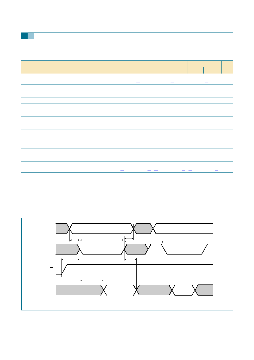
9397 750 13133
© Koninklijke Philips Electronics N.V. 2005. All rights reserved.
Product data sheet
Rev. 01 -- 9 February 2005
37 of 51
Philips Semiconductors
SC16C554B/554DB
5 V, 3.3 V and 2.5 V quad UART, 5 Mbit/s (max.) with 16-byte FIFOs
[1]
Applies to external clock, crystal oscillator max 24 MHz.
[2]
Maximum frequency =
[3]
RCLK is an internal signal derived from Divisor Latch LSB (DLL) and Divisor Latch MSB (DLM) divisor latches.
10.1 Timing diagrams
t
28d
delay from start to reset
TXRDY
-
8 T
RCLK
[3]
-
8 T
RCLK
[3]
-
8 T
RCLK
[3]
ns
t
30s
address setup time
10
-
10
-
10
-
ns
t
30w
chip select strobe width
25 pF load
[1]
90
-
26
-
23
-
ns
t
30h
address hold time
15
-
15
-
15
-
ns
t
30d
read cycle delay
25 pF load
20
-
20
-
20
-
ns
t
31d
delay from CS to data
25 pF load
-
90
-
26
-
23
ns
t
31h
data disable time
25 pF load
-
15
-
15
-
15
ns
t
32s
write strobe setup time
10
-
10
-
10
-
ns
t
32h
write strobe hold time
10
-
10
-
10
-
ns
t
32d
write cycle delay
25
-
25
-
20
-
ns
t
33s
data setup time
20
-
15
-
15
-
ns
t
33h
data hold time
15
-
5
-
5
-
ns
t
RESET
RESET pulse width
200
-
40
-
40
-
ns
N
baud rate divisor
1 T
RCLK
[3]
2
16
-
1
T
RCLK
[3]
1 T
RCLK
[3]
2
16
-
1
T
RCLK
[3]
1 T
RCLK
[3]
2
16
-
1
T
RCLK
[3]
ns
Table 26:
Dynamic characteristics
...continued
T
amb
=
-
40
∞
C to +85
∞
C; V
CC
= 2.5 V, 3.3 V or 5.0 V
±
10 %, unless otherwise specified.
Symbol Parameter
Conditions
2.5 V
3.3 V
5.0 V
Unit
Min
Max
Min
Max
Min
Max
1
t
3w
-------
Fig 14. General read timing in 68 mode
002aaa210
t
30s
A0 to A4
CS
R/W
D0 to D7
t
30w
t
30h
t
30d
t
31h
t
32s
t
31d
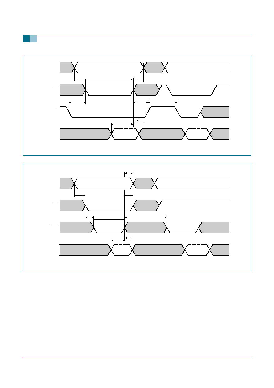
9397 750 13133
© Koninklijke Philips Electronics N.V. 2005. All rights reserved.
Product data sheet
Rev. 01 -- 9 February 2005
38 of 51
Philips Semiconductors
SC16C554B/554DB
5 V, 3.3 V and 2.5 V quad UART, 5 Mbit/s (max.) with 16-byte FIFOs
Fig 15. General write timing in 68 mode
002aaa211
A0 to A4
D0 to D7
CS
R/W
t
32s
t
33s
t
33h
t
32h
t
32d
t
30h
t
30w
t
30s
Fig 16. General write timing in 16 mode
data
active
active
valid
address
002aaa171
A0 to A2
CS
IOW
D0 to D7
t
16s
t
16h
t
13d
t
13w
t
15d
t
6h
t
13h
t
6s
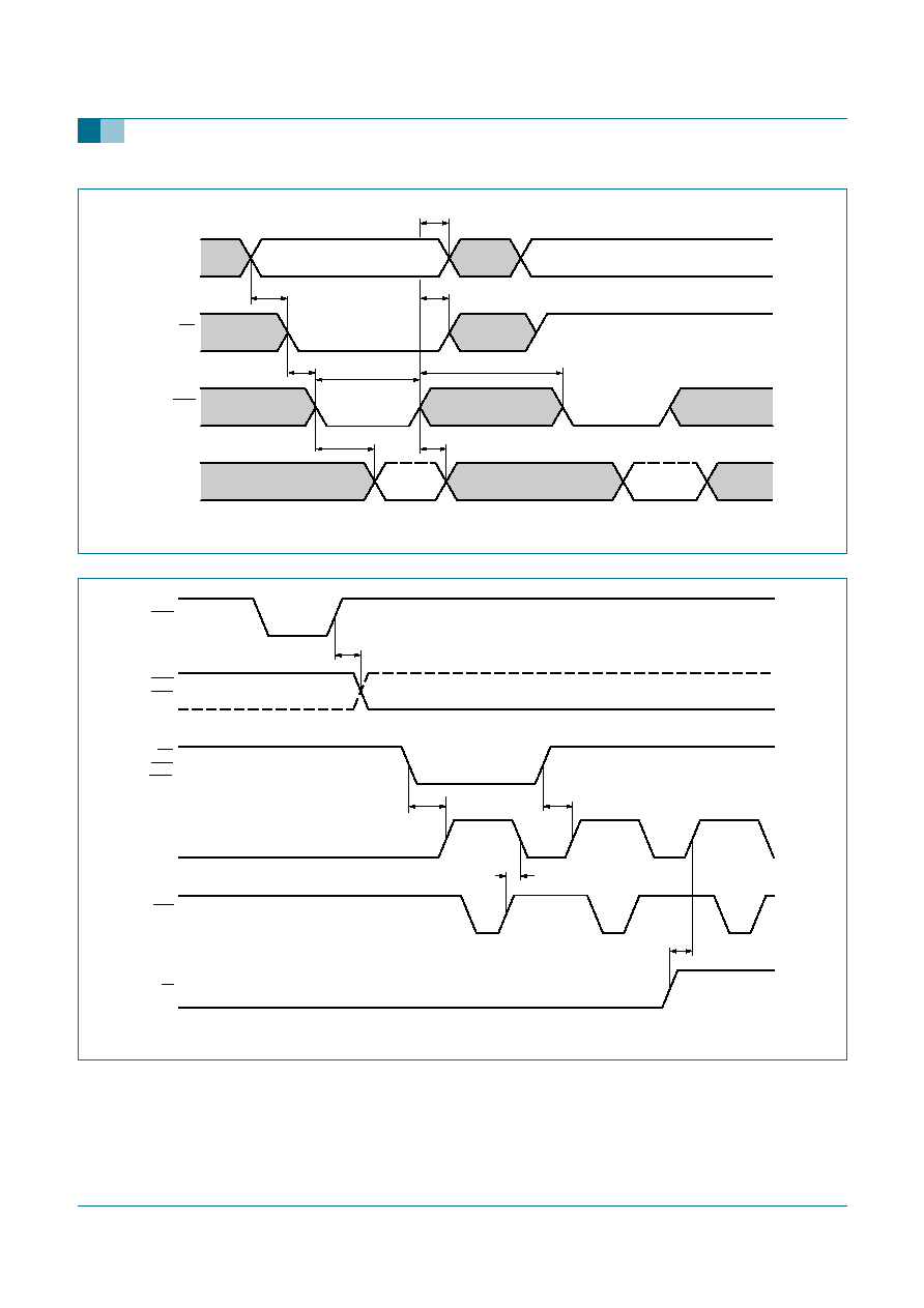
9397 750 13133
© Koninklijke Philips Electronics N.V. 2005. All rights reserved.
Product data sheet
Rev. 01 -- 9 February 2005
39 of 51
Philips Semiconductors
SC16C554B/554DB
5 V, 3.3 V and 2.5 V quad UART, 5 Mbit/s (max.) with 16-byte FIFOs
Fig 17. General read timing in 16 mode
data
active
active
valid
address
002aaa172
A0 to A2
CS
IOR
D0 to D7
t
12d
t
12h
t
7d
t
7w
t
9d
t
6h
t
7h
t
6s
Fig 18. Modem input/output timing
t
17d
change of state
t
18d
t
18d
t
19d
002aaa352
t
18d
change of state
change of state
change of state
active
active
active
active
active
active
active
change of state
RTS
DTR
IOW
CD
CTS
DSR
INT
IOR
RI
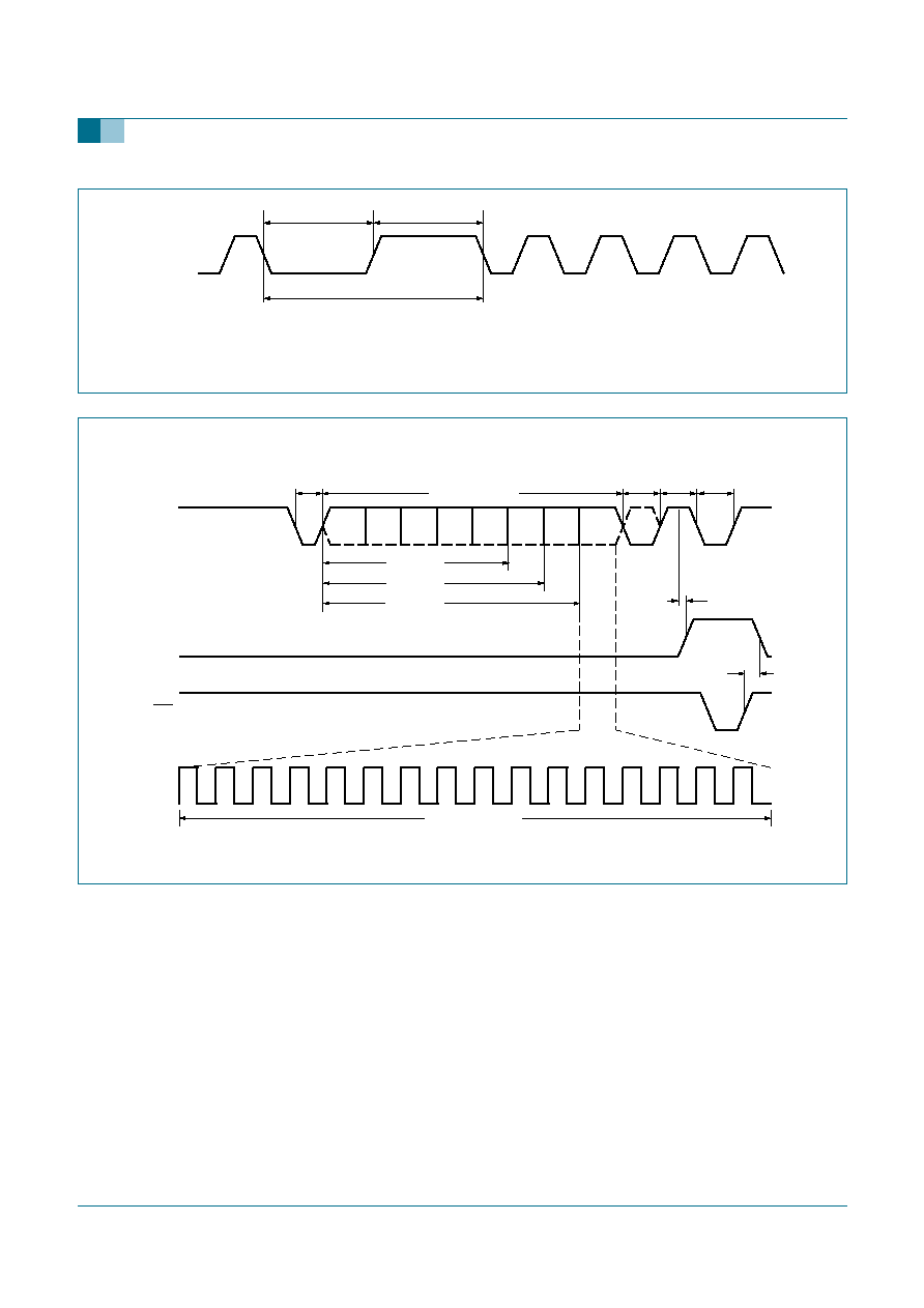
9397 750 13133
© Koninklijke Philips Electronics N.V. 2005. All rights reserved.
Product data sheet
Rev. 01 -- 9 February 2005
40 of 51
Philips Semiconductors
SC16C554B/554DB
5 V, 3.3 V and 2.5 V quad UART, 5 Mbit/s (max.) with 16-byte FIFOs
Fig 19. External clock timing
EXTERNAL
CLOCK
002aaa112
t
3w
t
2w
t
1w
f
XTAL
1
t
3w
-------
=
Fig 20. Receive timing
D0
D1
D2
D3
D4
D5
D6
D7
active
active
16 baud rate clock
002aaa113
RX
INT
IOR
t
21d
t
20d
5 data bits
6 data bits
7 data bits
stop
bit
parity
bit
start
bit
data bits (0 to 7)
next
data
start
bit
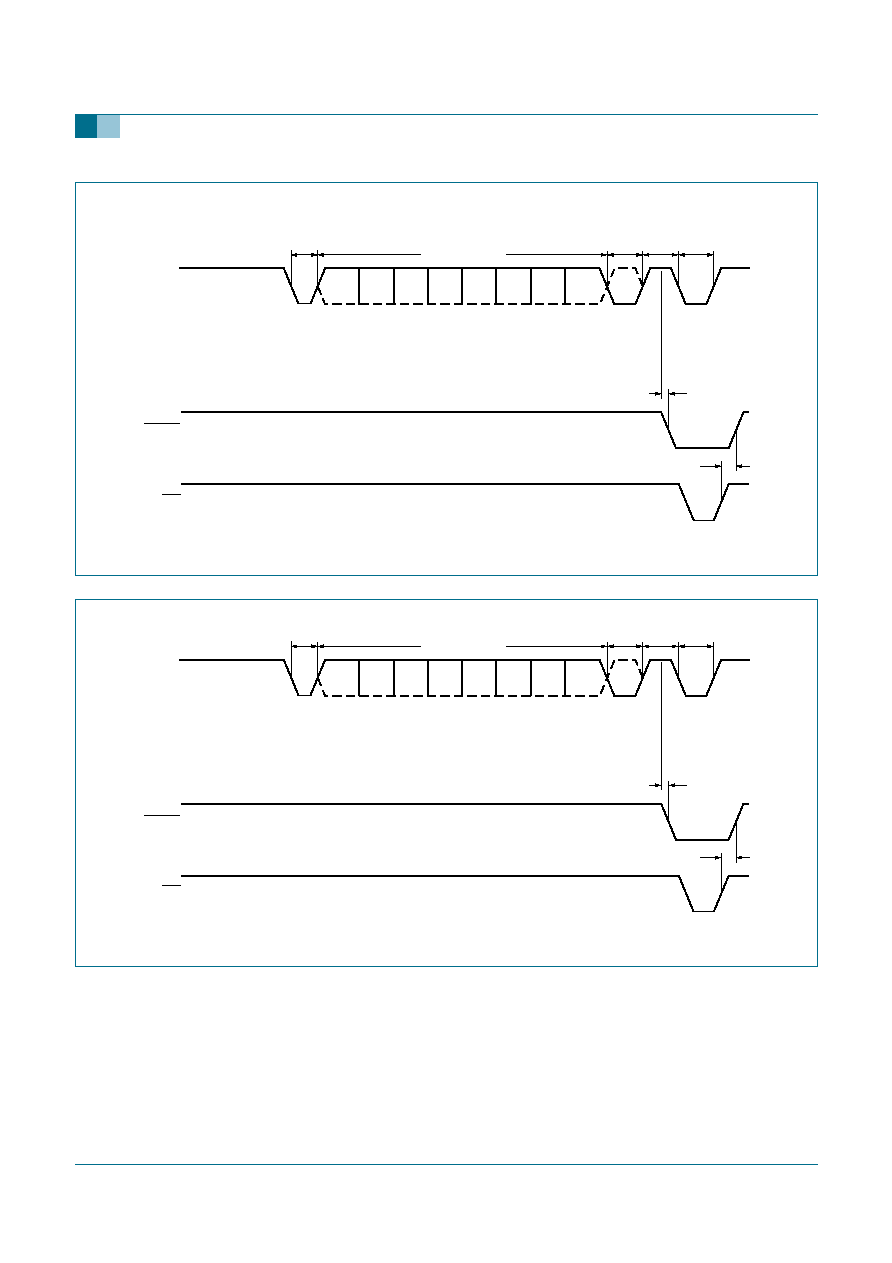
9397 750 13133
© Koninklijke Philips Electronics N.V. 2005. All rights reserved.
Product data sheet
Rev. 01 -- 9 February 2005
41 of 51
Philips Semiconductors
SC16C554B/554DB
5 V, 3.3 V and 2.5 V quad UART, 5 Mbit/s (max.) with 16-byte FIFOs
Fig 21. Receive ready timing in non-FIFO mode
D0
D1
D2
D3
D4
D5
D6
D7
002aab063
next
data
start
bit
stop
bit
parity
bit
t
25d
RX
RXRDY
IOR
active data
ready
start
bit
data bits (0 to 7)
active
t
26d
Fig 22. Receive ready timing in FIFO mode
D0
D1
D2
D3
D4
D5
D6
D7
002aab064
first byte that
reaches the
trigger level
stop
bit
parity
bit
t
25d
RX
RXRDY
IOR
active data
ready
start
bit
data bits (0 to 7)
active
t
26d
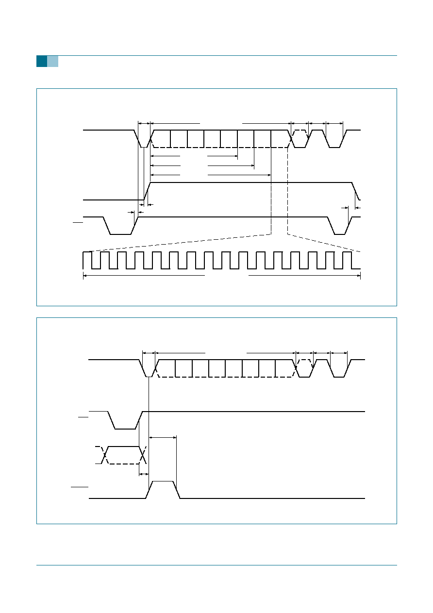
9397 750 13133
© Koninklijke Philips Electronics N.V. 2005. All rights reserved.
Product data sheet
Rev. 01 -- 9 February 2005
42 of 51
Philips Semiconductors
SC16C554B/554DB
5 V, 3.3 V and 2.5 V quad UART, 5 Mbit/s (max.) with 16-byte FIFOs
Fig 23. Transmit timing
active
transmitter ready
active
16 baud rate clock
002aaa116
t
24d
INT
IOW
active
D0
D1
D2
D3
D4
D5
D6
D7
TX
5 data bits
6 data bits
7 data bits
stop
bit
parity
bit
start
bit
data bits (0 to 7)
next
data
start
bit
t
22d
t
23d
Fig 24. Transmit ready timing in non-FIFO mode
D0
D1
D2
D3
D4
D5
D6
D7
002aab062
stop
bit
parity
bit
t
27d
TX
IOW
D0 to D7
active transmitter
ready
start
bit
data bits (0 to 7)
next
data
start
bit
byte #1
TXRDY
t
28d
transmitter
not ready
active
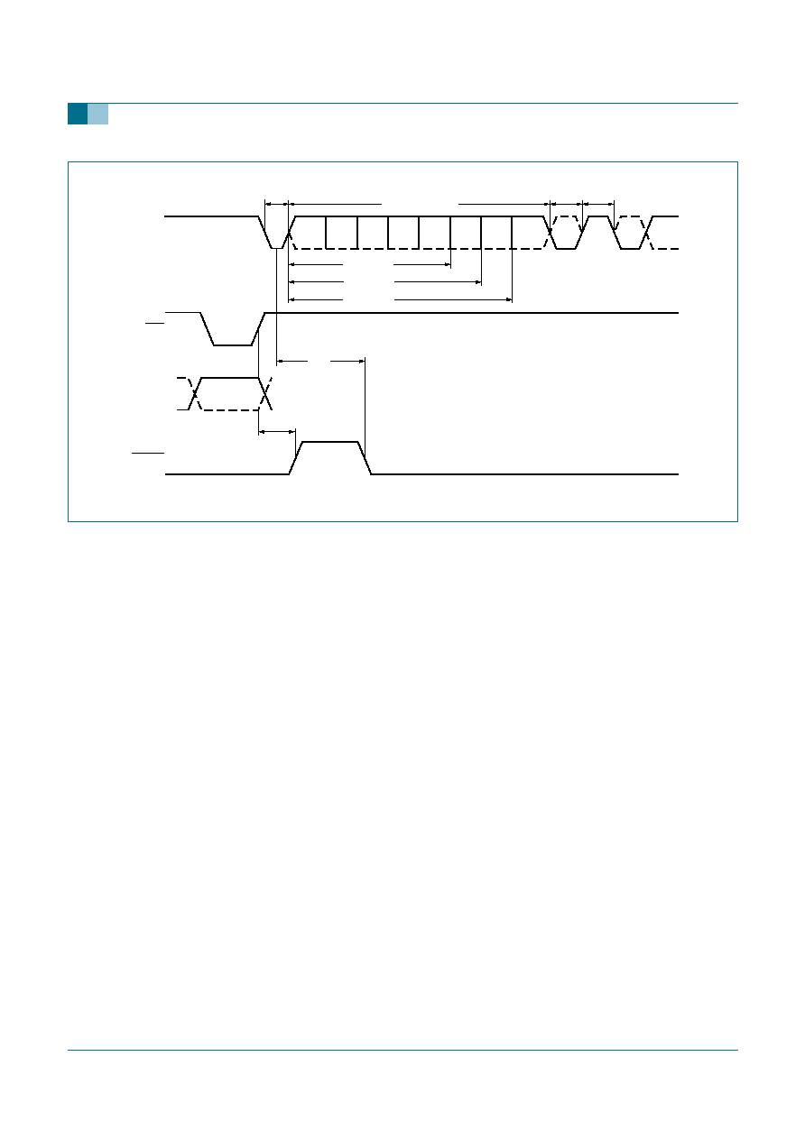
9397 750 13133
© Koninklijke Philips Electronics N.V. 2005. All rights reserved.
Product data sheet
Rev. 01 -- 9 February 2005
43 of 51
Philips Semiconductors
SC16C554B/554DB
5 V, 3.3 V and 2.5 V quad UART, 5 Mbit/s (max.) with 16-byte FIFOs
Fig 25. Transmit ready timing in FIFO mode (DMA mode `1')
D0
D1
D2
D3
D4
D5
D6
D7
002aab061
stop
bit
parity
bit
t
27d
TX
IOW
D0 to D7
start
bit
data bits (0 to 7)
byte #16
TXRDY
t
28d
FIFO full
active
5 data bits
6 data bits
7 data bits
9397 750 13133
© Koninklijke Philips Electronics N.V. 2005. All rights reserved.
Product data sheet
Rev. 01 -- 9 February 2005
44 of 51
Philips Semiconductors
SC16C554B/554DB
5 V, 3.3 V and 2.5 V quad UART, 5 Mbit/s (max.) with 16-byte FIFOs
11. Package outline
Fig 26. PLCC68 package outline (SOT188-2)
REFERENCES
OUTLINE
VERSION
EUROPEAN
PROJECTION
ISSUE DATE
IEC
JEDEC
JEITA
Note
1. Plastic or metal protrusions of 0.25 mm (0.01 inch) maximum per side are not included.
SOT188-2
44
60
68
1
9
10
26
43
27
61
detail X
(A )
3
b
p
w
M
A
1
A
A
4
L
p
b
1
k
X
y
e
E
B
D
H
E
H
v
M
B
D
Z D
A
Z E
e
v
M
A
pin 1 index
112E10
MS-018
EDR-7319
0
5
10 mm
scale
99-12-27
01-11-14
PLCC68: plastic leaded chip carrier; 68 leads
SOT188-2
UNIT
mm
4.57
4.19
0.51
3.3
0.53
0.33
0.021
0.013
1.27
2.16
45
o
0.18
0.1
0.18
DIMENSIONS (mm dimensions are derived from the original inch dimensions)
24.33
24.13
25.27
25.02
2.16
0.81
0.66
1.22
1.07
0.180
0.165
0.02
0.13
0.25
0.01
0.05
0.085
0.007 0.004
0.007
1.44
1.02
0.057
0.040
0.958
0.950
24.33
24.13
0.958
0.950
0.995
0.985
25.27
25.02
0.995
0.985
23.62
22.61
0.93
0.89
23.62
22.61
0.93
0.89
0.085
0.032
0.026
0.048
0.042
E
e
inches
D
e
A
A1
min.
A4
max.
bp
e
y
w
v
D
(1)
E
(1)
HD
HE
ZD
(1)
max.
ZE
(1)
max.
b1
k
A3
Lp
eD
eE
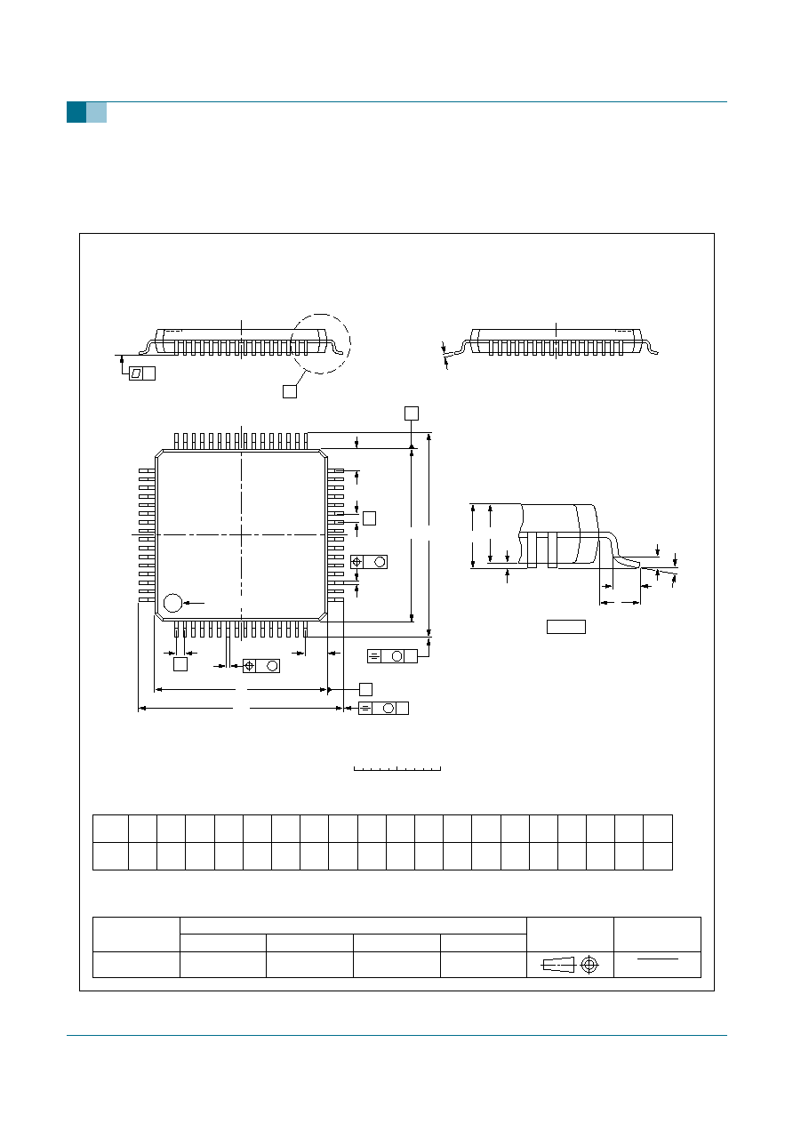
9397 750 13133
© Koninklijke Philips Electronics N.V. 2005. All rights reserved.
Product data sheet
Rev. 01 -- 9 February 2005
45 of 51
Philips Semiconductors
SC16C554B/554DB
5 V, 3.3 V and 2.5 V quad UART, 5 Mbit/s (max.) with 16-byte FIFOs
Fig 27. LQFP64 package outline (SOT314-2)
UNIT
A
max.
A
1
A
2
A
3
b
p
c
E
(1)
e
H
E
L
L
p
Z
y
w
v
REFERENCES
OUTLINE
VERSION
EUROPEAN
PROJECTION
ISSUE DATE
IEC
JEDEC
JEITA
mm
1.6
0.20
0.05
1.45
1.35
0.25
0.27
0.17
0.18
0.12
10.1
9.9
0.5
12.15
11.85
1.45
1.05
7
0
o
o
0.12
0.1
1
0.2
DIMENSIONS (mm are the original dimensions)
Note
1. Plastic or metal protrusions of 0.25 mm maximum per side are not included.
0.75
0.45
SOT314-2
MS-026
136E10
00-01-19
03-02-25
D
(1)
(1)
(1)
10.1
9.9
H
D
12.15
11.85
E
Z
1.45
1.05
D
b
p
e
E
A
1
A
L
p
detail X
L
(A )
3
B
16
c
D
H
b
p
E
H
A
2
v
M
B
D
Z D
A
Z E
e
v
M
A
X
1
64
49
48
33
32
17
y
pin 1 index
w
M
w
M
0
2.5
5 mm
scale
LQFP64: plastic low profile quad flat package; 64 leads; body 10 x 10 x 1.4 mm
SOT314-2
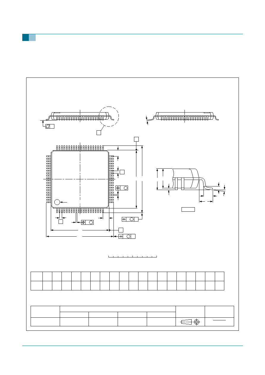
9397 750 13133
© Koninklijke Philips Electronics N.V. 2005. All rights reserved.
Product data sheet
Rev. 01 -- 9 February 2005
46 of 51
Philips Semiconductors
SC16C554B/554DB
5 V, 3.3 V and 2.5 V quad UART, 5 Mbit/s (max.) with 16-byte FIFOs
Fig 28. LQFP80 package outline (SOT315-1)
UNIT
A
max.
A
1
A
2
A
3
b
p
c
E
(1)
e
H
E
L
L
p
Z
y
w
v
REFERENCES
OUTLINE
VERSION
EUROPEAN
PROJECTION
ISSUE DATE
IEC
JEDEC
JEITA
mm
1.6
0.16
0.04
1.5
1.3
0.25
0.27
0.13
0.18
0.12
12.1
11.9
0.5
14.15
13.85
1.45
1.05
7
0
o
o
0.15
0.1
0.2
1
DIMENSIONS (mm are the original dimensions)
Note
1. Plastic or metal protrusions of 0.25 mm maximum per side are not included.
0.75
0.30
SOT315-1
136E15
MS-026
00-01-19
03-02-25
D
(1)
(1)
(1)
12.1
11.9
H
D
14.15
13.85
E
Z
1.45
1.05
D
b
p
e
E
A
1
A
L
p
detail X
L
(A )
3
B
20
c
D
H
b
p
E
H
A
2
v
M
B
D
Z D
A
Z E
e
v
M
A
X
1
80
61
60
41
40
21
y
pin 1 index
w
M
w
M
0
5
10 mm
scale
LQFP80: plastic low profile quad flat package; 80 leads; body 12 x 12 x 1.4 mm
SOT315-1

9397 750 13133
© Koninklijke Philips Electronics N.V. 2005. All rights reserved.
Product data sheet
Rev. 01 -- 9 February 2005
47 of 51
Philips Semiconductors
SC16C554B/554DB
5 V, 3.3 V and 2.5 V quad UART, 5 Mbit/s (max.) with 16-byte FIFOs
12. Soldering
12.1 Introduction to soldering surface mount packages
This text gives a very brief insight to a complex technology. A more in-depth account of
soldering ICs can be found in our
Data Handbook IC26; Integrated Circuit Packages
(document order number 9398 652 90011).
There is no soldering method that is ideal for all surface mount IC packages. Wave
soldering can still be used for certain surface mount ICs, but it is not suitable for fine pitch
SMDs. In these situations reflow soldering is recommended.
12.2 Reflow soldering
Reflow soldering requires solder paste (a suspension of fine solder particles, flux and
binding agent) to be applied to the printed-circuit board by screen printing, stencilling or
pressure-syringe dispensing before package placement. Driven by legislation and
environmental forces the worldwide use of lead-free solder pastes is increasing.
Several methods exist for reflowing; for example, convection or convection/infrared
heating in a conveyor type oven. Throughput times (preheating, soldering and cooling)
vary between 100 seconds and 200 seconds depending on heating method.
Typical reflow peak temperatures range from 215
∞
C to 270
∞
C depending on solder paste
material. The top-surface temperature of the packages should preferably be kept:
∑
below 225
∞
C (SnPb process) or below 245
∞
C (Pb-free process)
≠ for all BGA, HTSSON..T and SSOP..T packages
≠ for packages with a thickness
2.5 mm
≠ for packages with a thickness < 2.5 mm and a volume
350 mm
3
so called
thick/large packages.
∑
below 240
∞
C (SnPb process) or below 260
∞
C (Pb-free process) for packages with a
thickness < 2.5 mm and a volume < 350 mm
3
so called small/thin packages.
Moisture sensitivity precautions, as indicated on packing, must be respected at all times.
12.3 Wave soldering
Conventional single wave soldering is not recommended for surface mount devices
(SMDs) or printed-circuit boards with a high component density, as solder bridging and
non-wetting can present major problems.
To overcome these problems the double-wave soldering method was specifically
developed.
If wave soldering is used the following conditions must be observed for optimal results:
∑
Use a double-wave soldering method comprising a turbulent wave with high upward
pressure followed by a smooth laminar wave.
∑
For packages with leads on two sides and a pitch (e):
≠ larger than or equal to 1.27 mm, the footprint longitudinal axis is preferred to be
parallel to the transport direction of the printed-circuit board;

9397 750 13133
© Koninklijke Philips Electronics N.V. 2005. All rights reserved.
Product data sheet
Rev. 01 -- 9 February 2005
48 of 51
Philips Semiconductors
SC16C554B/554DB
5 V, 3.3 V and 2.5 V quad UART, 5 Mbit/s (max.) with 16-byte FIFOs
≠ smaller than 1.27 mm, the footprint longitudinal axis must be parallel to the
transport direction of the printed-circuit board.
The footprint must incorporate solder thieves at the downstream end.
∑
For packages with leads on four sides, the footprint must be placed at a 45
∞
angle to
the transport direction of the printed-circuit board. The footprint must incorporate
solder thieves downstream and at the side corners.
During placement and before soldering, the package must be fixed with a droplet of
adhesive. The adhesive can be applied by screen printing, pin transfer or syringe
dispensing. The package can be soldered after the adhesive is cured.
Typical dwell time of the leads in the wave ranges from 3 seconds to 4 seconds at 250
∞
C
or 265
∞
C, depending on solder material applied, SnPb or Pb-free respectively.
A mildly-activated flux will eliminate the need for removal of corrosive residues in most
applications.
12.4 Manual soldering
Fix the component by first soldering two diagonally-opposite end leads. Use a low voltage
(24 V or less) soldering iron applied to the flat part of the lead. Contact time must be
limited to 10 seconds at up to 300
∞
C.
When using a dedicated tool, all other leads can be soldered in one operation within
2 seconds to 5 seconds between 270
∞
C and 320
∞
C.
12.5 Package related soldering information
[1]
For more detailed information on the BGA packages refer to the
(LF)BGA Application Note (AN01026);
order a copy from your Philips Semiconductors sales office.
[2]
All surface mount (SMD) packages are moisture sensitive. Depending upon the moisture content, the
maximum temperature (with respect to time) and body size of the package, there is a risk that internal or
external package cracks may occur due to vaporization of the moisture in them (the so called popcorn
effect). For details, refer to the Drypack information in the
Data Handbook IC26; Integrated Circuit
Packages; Section: Packing Methods.
[3]
These transparent plastic packages are extremely sensitive to reflow soldering conditions and must on no
account be processed through more than one soldering cycle or subjected to infrared reflow soldering with
peak temperature exceeding 217
∞
C
±
10
∞
C measured in the atmosphere of the reflow oven. The package
body peak temperature must be kept as low as possible.
Table 27:
Suitability of surface mount IC packages for wave and reflow soldering methods
Package
[1]
Soldering method
Wave
Reflow
[2]
BGA, HTSSON..T
[3]
, LBGA, LFBGA, SQFP,
SSOP..T
[3]
, TFBGA, VFBGA, XSON
not suitable
suitable
DHVQFN, HBCC, HBGA, HLQFP, HSO, HSOP,
HSQFP, HSSON, HTQFP, HTSSOP, HVQFN,
HVSON, SMS
not suitable
[4]
suitable
PLCC
[5]
, SO, SOJ
suitable
suitable
LQFP, QFP, TQFP
not recommended
[5] [6]
suitable
SSOP, TSSOP, VSO, VSSOP
not recommended
[7]
suitable
CWQCCN..L
[8]
, PMFP
[9]
, WQCCN..L
[8]
not suitable
not suitable

9397 750 13133
© Koninklijke Philips Electronics N.V. 2005. All rights reserved.
Product data sheet
Rev. 01 -- 9 February 2005
49 of 51
Philips Semiconductors
SC16C554B/554DB
5 V, 3.3 V and 2.5 V quad UART, 5 Mbit/s (max.) with 16-byte FIFOs
[4]
These packages are not suitable for wave soldering. On versions with the heatsink on the bottom side, the
solder cannot penetrate between the printed-circuit board and the heatsink. On versions with the heatsink
on the top side, the solder might be deposited on the heatsink surface.
[5]
If wave soldering is considered, then the package must be placed at a 45
∞
angle to the solder wave
direction. The package footprint must incorporate solder thieves downstream and at the side corners.
[6]
Wave soldering is suitable for LQFP, QFP and TQFP packages with a pitch (e) larger than 0.8 mm; it is
definitely not suitable for packages with a pitch (e) equal to or smaller than 0.65 mm.
[7]
Wave soldering is suitable for SSOP, TSSOP, VSO and VSSOP packages with a pitch (e) equal to or larger
than 0.65 mm; it is definitely not suitable for packages with a pitch (e) equal to or smaller than 0.5 mm.
[8]
Image sensor packages in principle should not be soldered. They are mounted in sockets or delivered
pre-mounted on flex foil. However, the image sensor package can be mounted by the client on a flex foil by
using a hot bar soldering process. The appropriate soldering profile can be provided on request.
[9]
Hot bar soldering or manual soldering is suitable for PMFP packages.
13. Abbreviations
14. Revision history
Table 28:
Abbreviations
Acronym
Description
CPU
Central Processing Unit
DMA
Direct Memory Access
FIFO
First In/First Out
ISDN
Integrated Service Digital Network
QUART
4-channel (Quad) Universal Asynchronous Receiver and Transmitter
UART
Universal Asynchronous Receiver and Transmitter
Table 29:
Revision history
Document ID
Release date
Data sheet status
Change notice
Doc. number
Supersedes
SC16C554B_554DB_1
20050209
Product data sheet
-
9397 750 13133
-

Philips Semiconductors
SC16C554B/554DB
5 V, 3.3 V and 2.5 V quad UART, 5 Mbit/s (max.) with 16-byte FIFOs
9397 750 13133
© Koninklijke Philips Electronics N.V. 2005. All rights reserved.
Product data sheet
Rev. 01 -- 9 February 2005
50 of 51
15. Data sheet status
[1]
Please consult the most recently issued data sheet before initiating or completing a design.
[2]
The product status of the device(s) described in this data sheet may have changed since this data sheet was published. The latest information is available on the Internet at
URL http://www.semiconductors.philips.com.
[3]
For data sheets describing multiple type numbers, the highest-level product status determines the data sheet status.
16. Definitions
Short-form specification -- The data in a short-form specification is
extracted from a full data sheet with the same type number and title. For
detailed information see the relevant data sheet or data handbook.
Limiting values definition -- Limiting values given are in accordance with
the Absolute Maximum Rating System (IEC 60134). Stress above one or
more of the limiting values may cause permanent damage to the device.
These are stress ratings only and operation of the device at these or at any
other conditions above those given in the Characteristics sections of the
specification is not implied. Exposure to limiting values for extended periods
may affect device reliability.
Application information -- Applications that are described herein for any
of these products are for illustrative purposes only. Philips Semiconductors
make no representation or warranty that such applications will be suitable for
the specified use without further testing or modification.
17. Disclaimers
Life support -- These products are not designed for use in life support
appliances, devices, or systems where malfunction of these products can
reasonably be expected to result in personal injury. Philips Semiconductors
customers using or selling these products for use in such applications do so
at their own risk and agree to fully indemnify Philips Semiconductors for any
damages resulting from such application.
Right to make changes -- Philips Semiconductors reserves the right to
make changes in the products - including circuits, standard cells, and/or
software - described or contained herein in order to improve design and/or
performance. When the product is in full production (status `Production'),
relevant changes will be communicated via a Customer Product/Process
Change Notification (CPCN). Philips Semiconductors assumes no
responsibility or liability for the use of any of these products, conveys no
license or title under any patent, copyright, or mask work right to these
products, and makes no representations or warranties that these products are
free from patent, copyright, or mask work right infringement, unless otherwise
specified.
18. Trademarks
Intel -- is a registered trademark of Intel Corporation.
Motorola -- is a registered trademark of Motorola, Inc.
19. Contact information
For additional information, please visit: http://www.semiconductors.philips.com
For sales office addresses, send an email to: sales.addresses@www.semiconductors.philips.com
Level
Data sheet status
[1]
Product status
[2] [3]
Definition
I
Objective data
Development
This data sheet contains data from the objective specification for product development. Philips
Semiconductors reserves the right to change the specification in any manner without notice.
II
Preliminary data
Qualification
This data sheet contains data from the preliminary specification. Supplementary data will be published
at a later date. Philips Semiconductors reserves the right to change the specification without notice, in
order to improve the design and supply the best possible product.
III
Product data
Production
This data sheet contains data from the product specification. Philips Semiconductors reserves the
right to make changes at any time in order to improve the design, manufacturing and supply. Relevant
changes will be communicated via a Customer Product/Process Change Notification (CPCN).

© Koninklijke Philips Electronics N.V. 2005
All rights are reserved. Reproduction in whole or in part is prohibited without the prior
written consent of the copyright owner. The information presented in this document does
not form part of any quotation or contract, is believed to be accurate and reliable and may
be changed without notice. No liability will be accepted by the publisher for any
consequence of its use. Publication thereof does not convey nor imply any license under
patent- or other industrial or intellectual property rights.
Date of release: 9 February 2005
Document number: 9397 750 13133
Published in The Netherlands
Philips Semiconductors
SC16C554B/554DB
5 V, 3.3 V and 2.5 V quad UART, 5 Mbit/s (max.) with 16-byte FIFOs
20. Contents
1
General description . . . . . . . . . . . . . . . . . . . . . . 1
2
Features . . . . . . . . . . . . . . . . . . . . . . . . . . . . . . . 1
3
Ordering information . . . . . . . . . . . . . . . . . . . . . 2
4
Block diagram . . . . . . . . . . . . . . . . . . . . . . . . . . 3
5
Pinning information . . . . . . . . . . . . . . . . . . . . . . 5
5.1
Pinning . . . . . . . . . . . . . . . . . . . . . . . . . . . . . . . 5
5.1.1
PLCC68 . . . . . . . . . . . . . . . . . . . . . . . . . . . . . . 5
5.1.2
LQFP64 . . . . . . . . . . . . . . . . . . . . . . . . . . . . . . 7
5.1.3
LQFP80 . . . . . . . . . . . . . . . . . . . . . . . . . . . . . . 8
5.2
Pin description . . . . . . . . . . . . . . . . . . . . . . . . . 9
6
Functional description . . . . . . . . . . . . . . . . . . 13
6.1
Interface options . . . . . . . . . . . . . . . . . . . . . . . 14
6.1.1
The 16 mode interface . . . . . . . . . . . . . . . . . . 14
6.1.2
The 68 mode interface . . . . . . . . . . . . . . . . . . 14
6.2
Internal registers . . . . . . . . . . . . . . . . . . . . . . . 15
6.3
FIFO operation . . . . . . . . . . . . . . . . . . . . . . . . 15
6.4
Autoflow control (see
Figure 7
) . . . . . . . . . . . . 16
6.4.1
Auto-RTS (see
Figure 7
). . . . . . . . . . . . . . . . . 16
6.4.2
Auto-CTS (see
Figure 7
). . . . . . . . . . . . . . . . . 16
6.4.3
Enabling autoflow control and auto-CTS . . . . 17
6.4.4
Auto-CTS and auto-RTS functional timing . . . 17
6.5
Hardware/software and time-out interrupts. . . 18
6.6
Programmable baud rate generator . . . . . . . . 18
6.7
DMA operation . . . . . . . . . . . . . . . . . . . . . . . . 20
6.8
Loop-back mode . . . . . . . . . . . . . . . . . . . . . . . 20
7
Register descriptions . . . . . . . . . . . . . . . . . . . 23
7.1
Transmit (THR) and Receive (RHR) Holding
Registers. . . . . . . . . . . . . . . . . . . . . . . . . . . . . 24
7.2
Interrupt Enable Register (IER) . . . . . . . . . . . 24
7.2.1
IER versus Receive FIFO interrupt mode
operation. . . . . . . . . . . . . . . . . . . . . . . . . . . . . 25
7.2.2
IER versus Receive/Transmit FIFO polled mode
operation. . . . . . . . . . . . . . . . . . . . . . . . . . . . . 25
7.3
FIFO Control Register (FCR) . . . . . . . . . . . . . 25
7.3.1
DMA mode . . . . . . . . . . . . . . . . . . . . . . . . . . . 25
7.3.1.1
Mode 0 (FCR bit 3 = 0) . . . . . . . . . . . . . . . . . . 25
7.3.1.2
Mode 1 (FCR bit 3 = 1) . . . . . . . . . . . . . . . . . . 25
7.3.2
FIFO mode . . . . . . . . . . . . . . . . . . . . . . . . . . . 26
7.4
Interrupt Status Register (ISR) . . . . . . . . . . . . 27
7.5
Line Control Register (LCR) . . . . . . . . . . . . . . 28
7.6
Modem Control Register (MCR) . . . . . . . . . . . 30
7.7
Line Status Register (LSR) . . . . . . . . . . . . . . . 31
7.8
Modem Status Register (MSR). . . . . . . . . . . . 32
7.9
Scratchpad Register (SPR) . . . . . . . . . . . . . . 33
7.10
SC16C554B/554DB external reset
conditions . . . . . . . . . . . . . . . . . . . . . . . . . . . . 33
8
Limiting values . . . . . . . . . . . . . . . . . . . . . . . . 34
9
Static characteristics . . . . . . . . . . . . . . . . . . . 35
10
Dynamic characteristics . . . . . . . . . . . . . . . . . 36
10.1
Timing diagrams. . . . . . . . . . . . . . . . . . . . . . . 37
11
Package outline . . . . . . . . . . . . . . . . . . . . . . . . 44
12
Soldering . . . . . . . . . . . . . . . . . . . . . . . . . . . . . 47
12.1
Introduction to soldering surface mount
packages . . . . . . . . . . . . . . . . . . . . . . . . . . . . 47
12.2
Reflow soldering. . . . . . . . . . . . . . . . . . . . . . . 47
12.3
Wave soldering. . . . . . . . . . . . . . . . . . . . . . . . 47
12.4
Manual soldering . . . . . . . . . . . . . . . . . . . . . . 48
12.5
Package related soldering information . . . . . . 48
13
Abbreviations . . . . . . . . . . . . . . . . . . . . . . . . . 49
14
Revision history . . . . . . . . . . . . . . . . . . . . . . . 49
15
Data sheet status. . . . . . . . . . . . . . . . . . . . . . . 50
16
Definitions . . . . . . . . . . . . . . . . . . . . . . . . . . . . 50
17
Disclaimers . . . . . . . . . . . . . . . . . . . . . . . . . . . 50
18
Trademarks . . . . . . . . . . . . . . . . . . . . . . . . . . . 50
19
Contact information . . . . . . . . . . . . . . . . . . . . 50