Document Outline
- DESCRIPTION
- FEATURES
- OTHER FEATURES
- PIN CONFIGURATIONS
- APPLICATIONS
- ORDERING CODE
- BLOCK DIAGRAM
- ABSOLUTE MAXIMUM RATINGS
- DC ELECTRICAL CHARACTERISTICS
- CAPACITANCE
- AC ELECTRICAL CHARACTERISTICS
- BLOCK DIAGRAM
- Operation Control
- Timing
- Receiver
- Transmitter
- Modem Control
- SYN/DLE Control
- OPERATION
- EPCI PROGRAMMING
- Mode Register 1 (MR1)
- Mode Register 2 (MR2)
- Command Register (CR)
- Status Register
- AC LOAD CONDITIONS
- TIMING DIAGRAMS
- TYPICAL APPLICATIONS
Philips Semiconductors
Product specification
SCN2661/SCN68661
Enhanced programmable communications
interface (EPCI)
1
1994 Apr 27
853-1070 12793
DESCRIPTION
The Philips Semiconductors SCN2661 EPCI is a universal
synchronous/asynchronous data communications controller chip
that is an enhanced version of the SCN2651. It interfaces easily to
all 8-bit and 16-bit microprocessors and may be used in a polled or
interrupt driven system environment. The SCN2661 accepts
programmed instructions from the microprocessor while supporting
many serial data communications disciplines --synchronous and
asynchronous -- in the full- or half-duplex mode. Special support
for BISYNC is provided.
The EPCI serializes parallel data characters received from the
microprocessor for transmission. Simultaneously, it can receive
serial data and convert it into parallel data characters for input to the
microcomputer.
The SCN2661 contains a baud rate generator which can be
programmed to either accept an external clock or to generate
internal transmit or receive clocks. Sixteen different baud rates can
be selected under program control when operating in the internal
clock mode. Each version of the EPCI (A, B, C) has a different set
of baud rates.
FEATURES
�
Synchronous operation
� 5- to 8-bit characters plus parity
� Single or double SYN operation
� Internal or external character synchronization
� Transparent or non-transparent mode
� Transparent mode DLE stuffing (Tx) and detection (Rx)
� Automatic SYN or DLE-SYN insertion SYN, DLE and DLESYN
stripping
� Odd, even, or no parity
� Local or remote maintenance loopback mode
� Baud rate: DC to 1Mbps (1X clock)
�
Asynchronous operation
� 5- to 8-bit characters plus parity
� 1, 1-1/2 or 2 stop bits transmitted
� Odd, even, or no parity
� Parity, overrun and framing error detection
� Line break detection and generation
� False start bit detection
� Automatic serial echo mode (echoplex)
� Local or remote maintenance loopback mode
� Baud rate: DC to 1Mbps
(1X clock)
DC to 62.5kbps (16X clock)
DC to 15.625kbps
(64X clock)
OTHER FEATURES
�
Internal or external baud rate clock
�
3 baud rate sets
�
16 internal rates for each set
�
Double-buffered transmitter and receiver
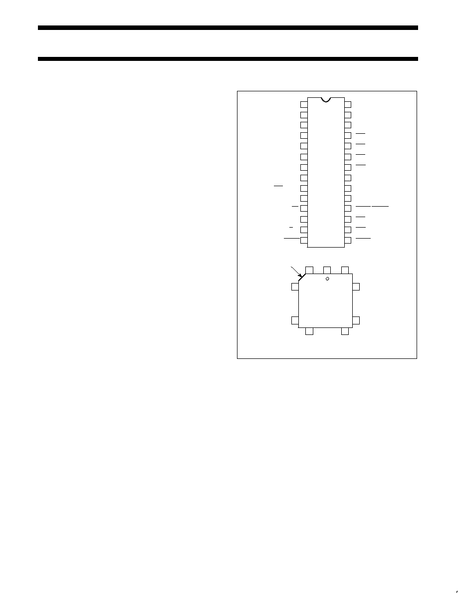
PIN CONFIGURATIONS
D1
D0
VCC
RxC/BKDET
DTR
RTS
DSR
RESET
BRCLK
TxD
TxEMT/DSCHG
CTS
DCD
TxRDY
RxRDY
R/W
A0
CE
A1
TxC/XSYNC
D7
D6
D5
D4
GND
RxD
D3
D2
DIP
PLCC
INDEX
CORNER
TOP VIEW
NOTE:
Pin Functions the same as 28-pin DIP.
28
27
26
25
24
23
22
21
20
19
18
17
16
15
1
2
3
4
5
6
7
8
9
10
11
12
13
14
26
25
19
18
12
11
5
4
1
SD00077
�
Dynamic character length switching
�
Full- or half-duplex operation
�
TTL compatible inputs and outputs
�
RxC and TxC pins are short-circuit protected
�
Single +5V power supply
�
No system clock required
APPLICATIONS
�
Intelligent terminals
�
Network processors
�
Front-end processors
�
Remote data concentrators
�
Computer-to-computer links
�
Serial peripherals
�
BISYNC adaptors
Philips Semiconductors
Product specification
SCN2661/SCN68661
Enhanced programmable communications
interface (EPCI)
1994 Apr 27
2
ORDERING CODE
PACKAGES
V
CC
= +5V +5%
DWG #
PACKAGES
Commercial
0
�
C to +70
�
C
Industrial
-40
�
C to +85
�
C
DWG #
28-Pin Ceramic Dual In-Line Package (cerdip) 0.6" Wide
SCN2661BC1F28
SCN2661CC1F28
SCN2661BA1F28
SCN2661CA1F28
0589B
28-Pin Plastic Dual In-Line Package (DIP) 0.6" Wide
SCN2661AC1N28
SCN2661BC1N28
SCN2661CC1N28
Contact Factory
SOT117-2
28-Pin Plastic Lead Chip Carrier (PLCC)
SCN2661AC1A28
SCN2661BC1A28
SCN2661CC1A28
Contact Factory
SOT261-3
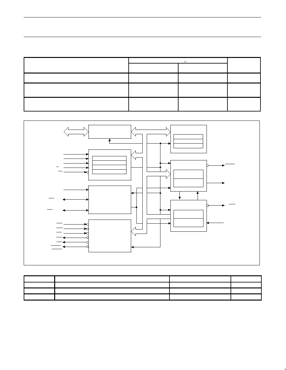
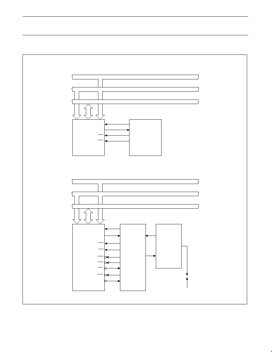
BLOCK DIAGRAM
DATA BUS
D0�D7
RESET
A
0
A
1
R/W
CE
DATA BUS
BUFFER
OPERATION CONTROL
MODE REGISTER 1
BAUD RATE
GENERATOR
AND
CLOCK CONTROL
SNE/DLE CONTROL
SYN 1 REGISTER
SYN 2 REGISTER
DLE REGISTER
TRANSMITTER
TRANSMIT DATA
TxD
MODE REGISTER 2
COMMAND REGISTER
STATUS REGISTER
BRCLK
TxC/SYNC
RxC/BKDET
DSR
MODEM
CONTROL
DCD
CTS
RTS
DTR
TxEMT/*
DSCHG
HOLDING REGISTER
TRANSMIT
SHIFT REGISTER
TxRDY
*
RECEIVE DATA
RECEIVE
RECEIVER
RxD
RxRDY
*
HOLDING REGISTER
SHIFT REGISTER
NOTES:
*
Open�drain output pin.
SD00078
ABSOLUTE MAXIMUM RATINGS
1
SYMBOL
PARAMETER
RATING
UNIT
T
A
Operating ambient temperature
2
Note 4
�
C
T
STG
Storage temperature
-65 to +150
�
C
All voltages with respect to ground
3
-0.5 to +6.0
V
NOTES:
1. Stresses above those listed under Absolute Maximum Ratings may cause permanent damage to the device. This is a stress rating only and
functional operation of the device at these or at any other condition above those indicated in the operation section of this specification is not
implied.
2. For operating at elevated temperatures, the device must be derated based on +150
�
C maximum function temperature.
3. This product includes circuitry specifically designed for the protection of its internal devices from the damaging effect of excessive static
charge. Nonetheless, it is suggested that conventional precautions be taken to avoid applying any voltages larger than the rated maxima.
4. Over recommended free-air operating temperature range and supply voltage range unless otherwise specified. For conditions shown as MIN
or MAX, use the appropriate value specified under recommended operating conditions.
Philips Semiconductors
Product specification
SCN2661/SCN68661
Enhanced programmable communications
interface (EPCI)
1994 Apr 27
3
DC ELECTRICAL CHARACTERISTICS
1, 2, 3
SYMBOL
PARAMETER
TEST CONDITIONS
LIMITS
UNIT
SYMBOL
PARAMETER
TEST CONDITIONS
Min
Typ
Max
UNIT
Input voltage
V
IL
V
IH
Low
High
2.0
0.8
V
V
Output voltage
V
OL
V
OH
4
Low
High
I
OL
= 2.2mA
I
OH
= -400
�
A
2.4
0.4
V
V
I
IL
Input leakage current
V
IN
= 0 to 5.5V
10
�
A
3-State output leakage current
I
LH
I
LL
Data bus high
Data bus low
V
O
= 4.0V
V
O
= 0.45V
10
10
�
A
�
A
I
CC
Power supply current
150
mA
NOTES:
1. Over recommended free-air operating temperature range and supply voltage range unless otherwise specified. For conditions shown as MIN
or MAX, use the appropriate value specified under recommended operating conditions.
2. All voltages measurements are referenced to ground. All time measurements are at the 50% level for inputs (except t
BRH
and t
BRL
) and at
0.8V and 2.0V for outputs. Input levels swing between 0.4V and 2.4V, with a transition time of
20ns maximum.
3. Typical values are at +25
�
C, typical supply voltages and typical processing parameters.
4. INTR, TxRDY, RxRDY and TxEMT/DSCHG outputs are open-drain.
CAPACITANCE
T
A
= 25
�
C, V
CC
= 0V
SYMBOL
PARAMETER
TEST CONDITIONS
LIMITS
UNIT
SYMBOL
PARAMETER
TEST CONDITIONS
Min
Typ
Max
UNIT
Capacitance
C
IN
C
OUT
C
I/O
Input
Output
Input/Output
f
C
= 1MHz
Unmeasured pins tied to ground
20
20
20
pF
pF
pF
Philips Semiconductors
Product specification
SCN2661/SCN68661
Enhanced programmable communications
interface (EPCI)
1994 Apr 27
4
AC ELECTRICAL CHARACTERISTICS
1, 2, 3
SYMBOL
PARAMETER
TEST CONDITIONS
LIMITS
UNIT
SYMBOL
PARAMETER
TEST CONDITIONS
Min
Typ
Max
UNIT
Pulse width
t
RES
t
CE
Reset
Chip enable
1000
250
ns
ns
Setup and hold time
t
AS
t
AH
t
CS
t
CH
t
DS
t
DH
t
RXS
t
RXH
Address setup
Address hold
R/W control setup
R/W control hold
Data setup for write
Data hold for write
RX data setup
RX data hold
10
10
10
10
150
10
300
350
ns
ns
ns
ns
ns
ns
ns
ns
t
DD
t
DF
7
t
CED
Data delay time for read
Data bus floating time for read
CE to CE delay
C
L
= 150pF
C
L
= 150pF
600
200
100
ns
ns
ns
Input clock frequency
f
BRG
f
BRG
f
R/T
6
Baud rate generator (2661A, B)
Baud rate generator (2661C)
TxC or RxC
1.0
1.0
dc
4.9152
5.0688
4.9202
5.0738
1.0
MHz
MHz
MHz
Clock width
t
BRH
5
t
BRH
5
t
BRL
5
t
BRL
5
t
R/TH
t
R/TL
6
Baud rate High (2661A, B)
Baud rate High (2661C)
Baud rate Low (2661A, B)
Baud rate Low (2661C)
TxC or RxC High
TxC or RxC Low
75
70
75
70
480
480
ns
ns
ns
ns
ns
ns
t
TXD
t
TCS
TxD delay from falling edge of TxC
Skew between TxD changing and falling
edge
of TxC output
4
C
L
= 150pF
C
L
= 150pF
0
650
ns
ns
NOTES:
1. Over recommended free-air operating temperature range and supply voltage range unless otherwise specified. For conditions shown as MIN
or MAX, use the appropriate value specified under recommended operating conditions.
2. All voltages measurements are referenced to ground. All time measurements are at the 50% level for inputs (except t
BRH
and t
BRL
) and at
0.8V and 2.0V for outputs. Input levels swing between 0.4V and 2.4V, with a transition time of
20ns maximum.
3. Typical values are at +25
�
C, typical supply voltages and typical processing parameters.
4. Parameter applies when internal transmitter clock is used.
5. Under test conditions of 5.0688MHz f
BRG
(68661) and 4.9152MHz f
BRG
(68661A, B), t
BRH
and t
BRL
measured at V
IH
and V
IL
, respectively.
6. In asynchronous local loopback mode, using 1X clock, the following parameters apply: f
R/T
= 0.83MHz max and t
R/TL
= 700ns min.
7. See AC load conditions.
BLOCK DIAGRAM
The EPCI consists of six major sections. These are the transmitter,
receiver, timing, operation control, modern control and SYN/DLE
control. These sections communicate with each other via an
internal data bus and an internal control bus. The internal data bus
interfaces to the microprocessor data bus via a data bus buffer.
Operation Control
This functional block stores configuration and operation commands
from the CPU and generates appropriate signals to various internal
sections to control the overall device operation. It contains read and
write circuits to permit communications with the microprocessor via
the data bus and contains mode registers 1 and 2, the command
register, and the status register. Details of register addressing and
protocol are presented in the EPCI programming section of this data
sheet.
Timing
The EPCI contains a Baud Rate Generator (BRG) which is
programmable to accept external transmit or receive clocks or to
divide an external clock to perform data communications. The unit
can generate 16 commonly used baud rates, any one of which can
be selected for full-duplex operation. See Table 1.
Receiver
The receiver accepts serial data on the RxD pin, converts this serial
input to parallel format, checks for bits or characters that are unique
to the communication technique and sends an "assembled"
character to the CPU.
Transmitter
The transmitter accepts parallel data from the CPU, converts it to a
serial bit stream, inserts the appropriate characters or bits (based on
Philips Semiconductors
Product specification
SCN2661/SCN68661
Enhanced programmable communications
interface (EPCI)
1994 Apr 27
5
the communication technique) and outputs a composite serial
stream of data on the TxD output pin.
Modem Control
The modern control section provides interfacing for three input
signals and three output signals used for "handshaking" and status
indication between the CPU and a modem.
SYN/DLE Control
This section contains control circuitry and three 8-bit registers
storing the SYN1, SYN2, and DLE characters provided by the CPU.
These registers are used in the synchronous mode of operation to
provide the characters required for synchronization, idle fill and data
transparency.
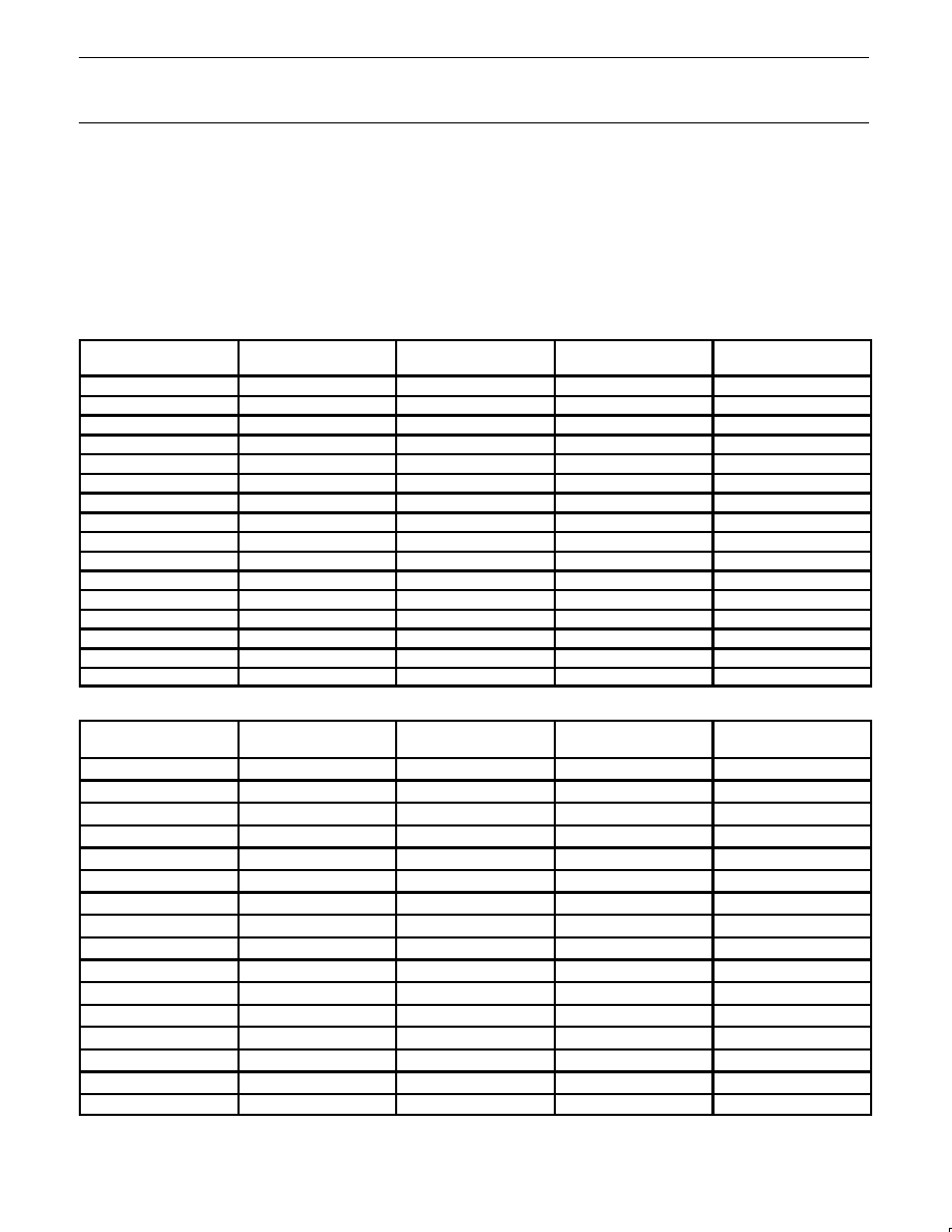
Table 1.
Baud Rate Generator Characteristics
68661A (BRCLK = 4.9152MHz)
MR23�20
BAUD RATE
ACTUAL FREQUENCY
16X CLOCK
PERCENT
ERROR
DIVISOR
0000
50
0.8kHz
--
6144
0001
75
1.2
--
4096
0010
110
1.7598
�0.01
2793
0011
134.5
2.152
--
2284
0100
150
2.4
--
2048
0101
200
3.2
--
1536
0110
300
4.8
--
1024
0111
600
9.6
--
512
1000
1050
16.8329
0.196
292
1001
1200
19.2
--
256
1010
1800
28.7438
�0.19
171
1011
2000
31.9168
�0.26
154
1100
2400
38.4
--
128
1101
4800
76.8
--
64
1110
9600
153.6
--
32
1111
19200
307.2
--
16
68661B (BRCLK = 4.9152MHz)
MR23�20
BAUD RATE
ACTUAL FREQUENCY
16X CLOCK
PERCENT
ERROR
DIVISOR
0000
45.5
0.7279kHz
0.005
6752
0001
50
0.8
--
6144
0010
75
1.2
--
4096
0011
110
1.7598
�0.01
2793
0100
134.5
2.152
--
2284
0101
150
2.4
--
2048
0110
300
4.8
--
1024
0111
600
9.6
--
512
1000
1200
19.2
--
256
1001
1800
28.7438
�0.19
171
1010
2000
31.9168
�0.26
154
1011
2400
38.4
--
128
1100
4800
76.8
--
64
1101
9600
153.6
--
32
1110
19200
307.2
--
16
1111
38400
614.4
--
8

Philips Semiconductors
Product specification
SCN2661/SCN68661
Enhanced programmable communications
interface (EPCI)
1994 Apr 27
6
68661C (BRCLK = 5.0688MHz)
MR23�20
BAUD RATE
ACTUAL FREQUENCY 16X CLOCK
PERCENT ERROR
DIVISOR
0000
50
0.8kHz
--
6336
0001
75
1.2
--
4224
0010
110
1.76
--
2880
0011
134.5
2.1523
0.016
2355
0100
150
2.4
--
2112
0101
300
4.8
--
1056
0110
600
9.6
--
528
0111
1200
19.2
--
264
1000
1800
28.8
--
176
1001
2000
32.081
0.253
158
1010
2400
38.4
--
132
1011
3600
57.6
--
88
1100
4800
76.8
--
66
1101
7200
115.2
--
44
1110
9600
153.6
--
33
1111
19200
316.8
3.125
16
NOTE: 16X clock is used in asynchronous mode. In synchronous mode, clock multiplier is 1X and BRG can be used only for TxC.
OPERATION
The functional operation of the 68661 is programmed by a set of
control words supplied by the CPU. These control words specify
items such as synchronous or asynchronous mode, baud rate,
number of bits per character, etc. The programming procedure is
described in the EPCI programming section of the data sheet.
After programming, the EPCI is ready to perform the desired
communications functions. The receiver performs serial to parallel
conversion of data received from a modem or equivalent device.
The transmitter converts parallel data received from the CPU to a
serial bit stream. These actions are accomplished within the
framework specified by the control words.
Receiver
The 68661 is conditioned to receiver data when the DCD input is
Low and the RxEN bit in the commands register is true. In the
asynchronous mode, the receiver looks for High-to-Low (mark to
space) transition of the start bit on the RxD input line. If a transition
is detected, the state of the RxD line is sampled again after a delay
of one-half of a bit-time. If RxD is now high, the search for a valid
start bit is begun again. If RxD is still Low, a valid start bit is
assumed and the receiver continues to sample the input line at one
bit time intervals until the proper number of data bits, the parity bit,
and one stop bit have been assembled. The data are then
transferred to the receive data holding register, the RxRDY bit in the
status register is set, and the RxRDY output is asserted. If the
character length is less than 8 bits, the High order unused bits in the
holding register are set to zero. The parity error, framing error, and
overrun error status bits are strobed into the status register on the
positive going edge of RxC corresponding to the received character
boundary. If the stop bit is present, the receiver will immediately
begin its search for the next start bit. If the stop bit is absent
(framing error), the receiver will interpret a space as a start bit if it
persists into the next bit timer interval. If a break condition is
detected (RxD is Low for the entire character as well as the stop bit),
only one character consisting of all zeros (with the FE status bit SR5
set) will be transferred to the holding register. The RxD input must
return to a High condition before a search for the next start bit
begins.
Pin 25 can be programmed to be a break detect output by
appropriate setting of MR27-MR24. If so, a detected break will
cause that pin to go High. When RxD returns to mark for one RxC
time, pin 25 will go low. Refer to the Break Detection Timing
Diagram.
When the EPCI is initialized into the synchronous mode, the
receiver first enters the hunt mode on a 0 to 1 transition of RxEN
(CR2). In this mode, as data are shifted into the receiver shift
register a bit at a time, the contents of the register are compared to
the contents of the SYN1 register. If the two are not equal, the next
bit is shifted in and the comparison is repeated. When the two
registers match, the hunt mode is terminated and character
assembly mode begins. If single SYN operation is programmed, the
SYN DETECT status bit is set. If double SYN operation is
programmed, the first character assembled after SYN1 must be
SYN2 in order for the SYN DETECT bit to be set. Otherwise, the
EPCI returns to the hunt mode. (Note that the sequence
SYN1-SYN1-SYN2 will not achieve synchronization.) When
synchronization has been achieved, the EPCI continues to
assemble characters and transfer then to the holding register,
setting the RxRDY status bit and asserting the RxRDY output each
time a character is transferred. The PE and OE status bits are set
as appropriate. Further receipt of the appropriate SYN sequence
sets the SYN DETECT status bit. If the SYN stripping mode is
commanded, SYN characters are not transferred to the holding
register. Note that the SYN characters used to establish initial
synchronization are not transferred to the holding register in any
case.
External jam synchronization can be achieved via pin 9 by
appropriate setting of MR27-MR24. When pin 9 is an XSYNC input,
the internal SYN1, SYN1�SYN2, and DLE�SYN1 detection is
disabled. Each positive going signal on XSYNC will cause the
receiver to establish synchronization on the rising edge of the next
RxC pulse. Character assembly will start with the RxD input at this
edge. XSYNC may be lowered on the next rising edge of RxD. This
external synchronization will cause the SYN DETECT status bit to
be set until the status register is read. Refer to XSYNC timing
diagram.

Philips Semiconductors
Product specification
SCN2661/SCN68661
Enhanced programmable communications
interface (EPCI)
1994 Apr 27
7
Table 2.
CPU-Related Signals
PIN NAME
PIN NO.
INPUT/
OUTPUT
FUNCTION
RESET
21
I
A High on this input performs a master reset on the 68661. This signal asynchronously
terminates any device activity and clears the mode, command and status registers. The
device assumes the idle state and remains there until initialized with the appropriate control
words.
A0, A1
12,10
I
Address lines used to select internal EPCI registers.
R/W
13
I
Read command when Low, write command when High.
CE
11
I
Chip enable command. When Low, indicates that control and data lines to the EPCI are
valid and that the operation specified by the RW, A1 and A0 inputs should be performed.
When High, places the D0�D7 lines in the 3-State condition.
D0�D7
27,28,1,2,5�8
I/O
8-bit, 3-State data bus used to transfer commands, data and status between EPCI and the
CPU. D0 is the least significant bit, D7 the most significant bit.
TxRDY
15
O
This output is the complement of status register bit SR0. When Low, it indicates that the
transmit data holding register (THR) is ready to accept a data character from the CPU. It
goes High when the data character is loaded. This output is valid only when the transmitter
is enabled. It is an open-drain output which can be used as an interrupt to the CPU.
RxRDY
14
O
This output is the complement of status register bit SR1. When Low, it indicates that the
receive data holding register (RHR) has a character ready for input to the CPU. It goes
High when the RHR is read by the CPU, and also when the receiver is disabled. It is an
open-drain output which can be used as an interrupt to the CPU.
TxEMT/DS
CHG
18
O
This output is the complement of status register bit SR2. When Low, it indicates that the
transmitter has completed serialization of the last character loaded by the CPU, or that a
change of state of the DSR or DCD inputs has occurred. This output goes High when the
status register is ready by the CPU, if the TxEMT condition does not exist. Otherwise, the
THR must be loaded by the CPU for this line to go high. It is an open-drain output which
can be used as an interrupt to the CPU. See Status Register (SR2) for details.
Table 3.
Device-Related Signals
PIN NAME
PIN NO.
INPUT/
OUTPUT
FUNCTION
BRCLK
20
I
Clock input to the internal baud rate generator (see Table 1). Not required if external
receiver and transmitter clocks are used.
RxC/BKDET
25
I/O
Receiver clock. If external receiver clock is programmed, this input controls the rate at
which the character is to be received. Its frequency is 1X, 16X or 64X the baud rate, as
programmed by mode register 1. Data are sampled on the rising edge of the clock. If
internal receiver clock is programmed, this pin can be a 1X/16X clock or a break detect
output pin.
TxC/XSYNC
9
I/O
Transmitter clock. If external transmitter clock is programmed, this input controls the rate at
which the character is transmitted. Its frequency is 1X, 16X or 64X the baud rate, as
programmed by mode register 1. The transmitted data changes on the falling edge of the
clock. If internal transmitter clock is programmed, this pin can be a 1X/16X clock output or
an external jam synchronization input.
RxD
3
I
Serial data input to the receiver. "Mark" is High, "space" is Low.
TxD
19
O
Serial data output from the transmitter. "Mark" is High, "Space" is Low. Held in mark
condition when the transmitter is disabled.
DSR
22
I
General purpose input which can be used for data set ready or ring indicator condition. Its
complement appears as status register bit SR7. Causes a Low output on TxEMT/DSCHG
when its state changes if CR2 or CR0 = 1.
DCD
16
I
Data carrier detect input. Must be Low in order for the receiver to operate. Its complement
appears as status register bit SR6. Causes a Low output on TxEMT/DSCHG when its
state changes if CR2 or CR0 = 1. If DCD goes High while receiving, the RxC is internally
inhibited.
CTS
17
I
Clear to send input. Must be Low in order for the transmitter to operate. If it goes High
during transmission, the character in the transmit shift register will be transmitted before
termination.
DTR
24
O
General purpose output which is the complement of command register bit CR1. Normally
used to indicate data terminal ready.
RTS
23
O
General purpose output which is the complement of command register bit CR5. Normally
used to indicate request to send. See Command Register (CR5) for details.

Philips Semiconductors
Product specification
SCN2661/SCN68661
Enhanced programmable communications
interface (EPCI)
1994 Apr 27
8
Transmitter
The EPCI is conditioned to transmit data when the CTS input is Low
and the TxEN command register bit is set. The 68661 indicates to
the CPU that it can accept a character for transmission by setting
the TxRDY status bit and asserting the TxRDY output. When the
CPU writes a character into the transmit data holding register, these
conditions are negated. Data are transferred from the holding
register to the transmit shift register when it is idle or has completed
transmission of the previous character. The TxRDY conditions are
then asserted again. Thus, one full character time of buffering is
provided.
In the asynchronous mode, the transmitter automatically sends a
start bit followed by the programmed number of data bits, the least
significant bit being sent first. It then appends an optional odd or
even parity bit and the programmed number of stop bits. If,
following transmission of the data bits, a new character is not
available in the transmit holding register, the TxD output remains in
the marking (High) condition and the TxEMT/DSCHG output and its
corresponding status bit are asserted. Transmission resumes when
the CPU loads a new character into the holding register. The
transmitter can be forced to output a continuous Low (BREAK)
condition by setting the send break command bit (CR3) High.
In the synchronous mode, when the 68661 is initially conditioned to
transmit, the TxD output remains High and the TxRDY condition is
asserted until the first character to be transmitted (usually a SYN
character) is loaded by the CPU. Subsequent to this, a continuous
stream of characters is transmitted. No extra bits (other than parity,
if commanded) are generated by the EPCI unless the CPU fails to
send a new character to the EPCI by the time the transmitter has
completed sending the previous character. Since synchronous
communication does not allow gaps between characters, the EPCI
asserts TxEMT and automatically "fills" the gap by transmitting
SYN1s, SYN1�SYN2 doublets, or DLE�SYN1 doubles, depending
on the state of MR16 and MR17. Normal transmission of the
message resumes when a new character is available in the transmit
data holding register. If the send DLE bit in the commands register
is true, the DLE character is automatically transmitted prior to
transmission of the message character in the THR.
EPCI PROGRAMMING
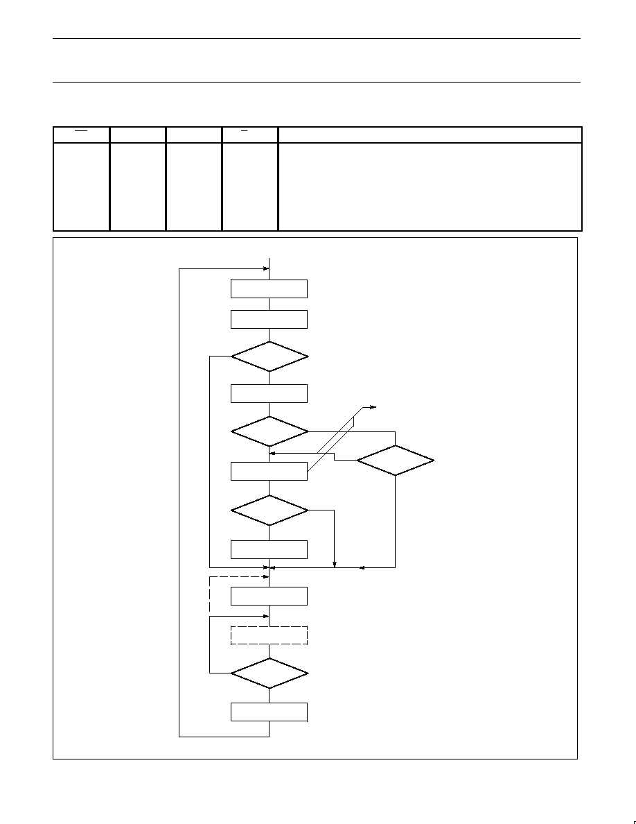
Prior to initiating data communications, the 68661 operational mode
must be programmed by performing write operations to the mode
and command registers. In addition, if synchronous operation is
programmed, the appropriate SYN/DLE registers must be loaded.
The EPCI can be reconfigured at any time during program
execution. A flowchart of the initialization process appears in
Figure 1.
The internal registers of the EPCI are accessed by applying specific
signals to the CE, R/W, A1 and A0 inputs. The conditions
necessary to address each register are shown in Table 4.
The SYN1, SYN2, and DLE registers are accessed by performing
write operations with the conditions A1 = 0, A0 = 1, and R/W = 1.
The first operation loads the SYN1 register. The next loads the DLE
register. Reading or loading the mode registers is done in a similar
manner. The first write (or read) operation addresses mode register
1, and a subsequent operation addresses mode register 2. If more
than the required number of accesses are made, the internal
sequencer recycles to point at the first register. The pointers are
reset to SYN1 register and mode register 1 by a RESET input or by
performing a read command register operation, but are unaffected
by any other read or write operation.
The 68661 register formats are summarized in Tables 5, 6, 7 and 8.
Mode registers 1 and 2 define the general operational
characteristics of the EPCI, while the command register controls the
operation within this basic framework. The EPCI indicates its status
in the status register. These registers are cleared when a RESET
input is applied.
Mode Register 1 (MR1)
Table 5 illustrates mode register 1. Bits MR11 and MR10 select the
communication format and baud rate multiplier. 00 specifies
synchronous format. However, the multiplier in asynchronous
format applies only if the external clock input option is selected by
MR24 or MR25.
MR13 and MR12 select a character length of 5, 6, 7 or 8 bits. The
character length does not include the parity bit, if programmed, and
does not include the start and stop bits in asynchronous mode.
MR14 controls parity generation. If enabled, a parity bit is added to
the transmitted character and the receiver performs a parity check
on incoming data. MR15 selects odd or even parity when parity is
enabled by MR14. In asynchronous mode, MR17 and MR16 select
character framing of 1, 1.5, or 2 stop bits. (If 2X baud rate is
programmed, 1.5 stop bits defaults to 1 stop bits on transmit.) In
synchronous mode, MR17 controls the number of SYN characters
used to establish synchronization and for character fill when the
transmitter is idle. SYN1 alone is used if MR17 = 1, and
SYN1�SYN2 is used when MR17 = 0. If the transparent mode is
specified by MR16, DLE�SYN1 is used for character fill and SYN
detect, but the normal synchronization sequence is used to establish
character sync. When transmitting, a DLE character in the transmit
holding register will cause a second DLE character to be
transmitted. This DLE stuffing eliminates the software DLE compare
and stuff on each transparent mode data character. If the send DLE
command (CR3) is active when a DLE is loaded into THR, only one
additional DLE will be transmitted. Also, DLE stripping and DLE
detect (with MR14 = 0) are enabled.
The bits in the mode register affecting character assembly and
disassembly (MR12�MR16) can be changed dynamically (during
active receive/transmit operation). The character mode register
affects both the transmitter and receiver; therefore in synchronous
mode, changes should be made only in half-duplex mode (RxEN = 1
or TxEN = 1, but not both simultaneously = 1). In asynchronous
mode, character changes should be made when RxEN and TxEN =
0 or when TxEN = 1 and the transmitter is marking in half-duplex
mode (RxEN = 0).
To effect assembly/disassembly of the next received/transmitted
character, MR12 � 15 must be changed within n bit times of the
active going state of RxRDY/TxRDY. Transparent and
non-transparent mode changes (MR16) must occur within n-1 bit
times of the character to be affected when the receiver or transmitter
is active. (n � smaller of the new and old character lengths.)
Philips Semiconductors
Product specification
SCN2661/SCN68661
Enhanced programmable communications
interface (EPCI)
1994 Apr 27
9
Table 4.
68661 Register Addressing
CE
A
1
A
0
R/W
FUNCTION
1
0
0
0
0
0
0
0
0
X
0
0
0
0
1
1
1
1
X
0
0
1
1
0
0
1
1
X
0
1
0
1
0
1
0
1
3-State data bus
Read receive holding register
Write transmit holding register
Read status register
Write SYN1/SYN2/DLE registers
Read mode register 1/2
Write mode register 1/2
Read command register
Write command register
LOAD
MODE REGISTER 1
LOAD
MODE REGISTER 2
SYNCHRONOUS?
LOAD
SYN 1 REGISTER
DOUBLE
SYNC?
LOAD
SYN 2 REGISTER
TRANSPARENT
MODE?
LOAD
DLE REGISTER
INITIAL RESET
N
Y
Y
N
N
Y
TRANSPARENT
MODE?
Y
N
LOAD
COMMAND REGISTER
OPERATE
RECONFIGURE?
N
Y
DISABLE
RCVR AND XMTR
NOTE:
SYN1 Register must be written
before SYN2 can be written, and
SYN2 before DLE can be written.
NOTE:
Mode Register 1 must be written
before 2 can be written. Mode Register 2
need not be programmed if external
clocks are used.
SD00079
Figure 1. 68661 Initialization Flowchart

Philips Semiconductors
Product specification
SCN2661/SCN68661
Enhanced programmable communications
interface (EPCI)
1994 Apr 27
10
Table 5.
Mode Register 1 (MR1)
MR17
MR16
MR15
MR14
MR13
MR12
MR11
MR10
Sync/Async
Parity Type
Parity Control
Character Length
Mode and Baud Rate Factor
Async: Stop bit length
00 = invalid
01 = 1 stop bit
10 = 1 1/2 stop bits
11 = 2 stop bits
0 = Odd
1 = Even
0 = Disabled
1 = Enabled
00 = 5 bits
01 = 6 bits
10 = 7 bits
11 = 8 bits
00 = Synchronous 1X rate
01 = Asynchronous 1X rate
10 = Asynchronous 16X rate
11 = Asynchronous 64X rate
Sync:
Number of
SYN char
0 = Double SYN
1 = Single SYN
Sync:
Transparency
control
0 = Normal
1 = Transparent
NOTE: Baud rate factor in asynchronous applies only if external clock is selected. Factor is 16X if internal clock is selected. Mode must be
selected (MR11, MR10) in any case.
Table 6.
Mode Register 2 (MR2)
MR27 � MR24
MR23 � MR20
TxC
RxC
Pin 9
Pin 25
TxC
RxC
Pin 9
Pin 25
Mode
Baud Rate
Selection
0000
0001
0010
0011
0100
0101
0110
0111
E
E
I
I
E
E
I
I
E
I
E
I
E
I
E
I
TxC
TxC
1X
1X
TxC
TxC
16X
16X
RxC
1X
RxC
1X
RxC
16X
RxC
16X
1000
1001
1010
1011
1100
1101
1110
1111
E
E
I
I
E
E
I
I
E
I
E
I
E
I
E
I
XSYNC*
TxC
XSYNC*
1X
XSYNC*
TXC
XSYNC*
16X
RXC/TxC
BKDET
RxC
BKDET
RxC/TxC
BKDET
RxC
BKDET
sync
async
sync
async
sync
async
sync
async
See baud rates
in Table 1.
NOTES:
*
When pin 9 is programmed as XSYNC input, SYN1, SYN1�SYN2, and DLE�SYN1 detection is disabled.
E = External clock
I
= Internal clock (BRG)
1X and 16X are clock outputs.
Table 7.
Command Register (CR)
CR7
CR6
CR5
CR4
CR3
CR2
CR1
CR0
Operating Mode
Request
to Send
Reset Error
Sync/Async
Receive
Control
(RxEN)
Data Terminal
Ready
Transmit
Control
(TxEN)
00 = Normal operation
01 = Async:
Automatic
Echo mode
Sync: SYN and/or DLE
stripping mode
10 = Local loopback
11 = Remote loopback
0 = Force RTS
Output High
one clock
time after
TxSR
serialization
1 = Force RTS
output Low
0 = Normal
1 = Reset error
flags in
status reg.
(FE,OE,PE/
DLE detect.)
Async:
Force Break
0 = Normal
1 = Force
break
Sync
Send DLE
0 = Normal
1 = Send DLE
0 = Disable
1 = Enable
Not applicable
in
0 = Force DTR
output High
1 = Force DTR
output Low
0 = Disable
1 = Enable

Philips Semiconductors
Product specification
SCN2661/SCN68661
Enhanced programmable communications
interface (EPCI)
1994 Apr 27
11
Table 8.
Status Register (SR)
SR7
SR6
SR5
SR4
SR3
SR2
SR1
SR0
Data Set
Ready
Data Carrier
Detect
FE/SYN
Detect
Overrun
PE/DLE
Detect
TxEMT
DSCHG
RxRDY
TxRDY
0 = DSR input
is High
1 = DSR input
is Low
0 = DCD input
is High
1 = DCD input
is Low
Async:
0 = Normal
1 = Framing
error
Sync:
0 = Normal
1 = SYN
detected
0 = Normal
1 = Overrun
error
Async:
0 = Normal
1 = Parity error
Sync:
0 = Normal
1 = Parity error
or DLE
received
0 = Normal
1 = Change in
DSR or
DCD, or
transmit
shift
register is
empty
0 = Receive
holding
register
empty
1 = Receive
holding
register
has data
0 = Transmit
holding
register
busy
1 = Transmit
holding
register
empty
Mode Register 2 (MR2)
Table 6 illustrates mode register 2. MR23, MR22, MR21 and MR20
control the frequency of the internal baud rate generator (BRG).
Sixteen rates are selectable for each EPCI version (�1,�2,�3).
Versions 1 and 2 specify a 4.9152MHz TTL input at BRCLK (pin 20);
version 3 specifies a 5.0688MHz input which is identical to the
Philips Semiconductors 2651. MR23 � 20 are don't cares if external
clocks are selected (MR25 � MR24 = 0). The individual rates are
given in Table 1.
MR24 � MR27 select the receive and transmit clock source (either
the BRG or an external input) and the function at pins 9 and 25.
Refer to Table 6.
Command Register (CR)
Table 7 illustrates the command register. Bits CR0 (TxEN) and CR2
(RxEN) enable or disable the transmitter and receiver respectively.
A 0� to�1 transition of CR2 forces start bit search (async mode) or
hunt mode (sync mode) on the second RxC rising edge. Disabling
the receiver causes RxRDY to go High (inactive). If the transmitter
is disabled, it will complete the transmission of the character in the
transmit shift register (if any) prior to terminating operation. The TxD
output will then remain in the marking state (High) while TxRDY and
TxEMT will go High (inactive). If the receiver is disabled, it will
terminate operation immediately. Any character being assembled
will be neglected. A 0�to�1 transition of CR2 will initiate start bit
search (async) or hunt mode (sync).
Bits CR1 (DTR) and CR5 (RTS) control the DTR and RTS outputs.
Data at the outputs are the logical complement of the register data.
In asynchronous mode, setting CR3 will force and hold the TxD
output Low (spacing condition) at the end of the current transmitted
character. Normal operation resumes when CR3 is cleared. The
TxD line will go High for at least one bit time before beginning
transmission of the next character in the transmit data holding
register. In synchronous mode, setting CR3 causes the
transmission of the DLE register contents prior to sending the
character in the transmit data holding register. Since this is a one
time command, CR3 does not have to be reset by software. CR3
should be set when entering and exiting transparent mode and for
all DLE-non-DLE character sequences.
Setting CR4 causes the error flags in the status register (SR3, SR4,
and SR5) to be cleared; this is a one time command. There is no
internal latch for this bit.
When CR5 (RTS) is set, the RTS pin is forced Low. A 1�to�0
transition of CR5 will cause RTS to go High (inactive) one TxC time
after the last serial bit has been transmitted. If a 1�to�0 transition
of CR5 occurs while data is being transmitted, RTS will remain Low
(active) until both the THR and the transmit shift register are empty
and then go High (inactive) one TxC time later.
The EPCI can operate in one of four submodes within each major
mode (synchronous or asynchronous). The operational sub-mode is
determined by CR7 and CR6. CR7 � CR6 = 00 is the normal mode,
with the transmitter and receive operating independently in
accordance with the mode and status register instructions.
In asynchronous mode, CR7 � CR6 = 01 places the EPCI in the
automatic echo mode. Clocked, regenerated received data are
automatically directed to the TxD line while normal receiver
operation continues. The receiver must be enabled (CR2 = 1), but
the transmitter need not be enabled. CPU to receiver
communication continues normally, but the CPU to transmitter link is
disabled. Only the first character of a break condition is echoed.
The TxD output will go High until the next valid start is detected.
The following conditions are true while in automatic echo mode:
1. Data assembled by the receiver are automatically placed in the
transmit holding register and retransmitted by the transmitter on
the TxD output.
2. The transmitter is clocked by the receive clock.
3. TxRDY output = 1.
4. The TxEMT/DSCHG pin will reflect only the data set change
condition.
5. The TxEN command (CR0) is ignored.
In synchronous mode, CR7 � CR6 = 01 places the EPCI in the
automatic SYN/DLE stripping mode. The exact action taken
depends on the setting of bits MR17 and MR16:
1. In the non-transparent, single SYN mode (MR17 � MR16 = 10),
characters in the data stream matching SYN1 are not transferred
to the Receive Data Holding register (RHR).
2. In the non-transparent, double SYN mode (MR17 � MR16 = 00),
character in the data stream matching SYN1, or SYN2 if immedi-
ately preceded by SYN1, are not transferred the RHR.
3. In transparent mode (MR16 = 1), character in the data stream
matching DLE, or SYN1 if immediately preceded by DLE, are not
transferred to the RHR. However, only the first DLE of a DLE�
DLE pair is stripped.
Note that automatic stripping mode does not affect the setting of the
DLE detect and SYN detect status bits (SR3 and SR5).
Two diagnostic sub-modes can also be configured. In local
loopback mode (CR7 � CR6 = 10), the following loops are
connected internally:

Philips Semiconductors
Product specification
SCN2661/SCN68661
Enhanced programmable communications
interface (EPCI)
1994 Apr 27
12
1. The transmitter output is connected to the receiver input.
2. DTR is connected to DCD and RTS is connected to CTS.
3. The receiver is clocked by the transmit clock.
4. The DTR, RTS and TxD outputs are held High.
5. The CTS, DCD, DSR and RxD inputs are ignored.
Additional requirements to operate in the local loopback mode are
that CR0 (TxEN), CR1 (DTR) and CR5 (RTS) must be set to 1.
CR2 (RxEN) is ignored by the EPCI.
The second diagnostic mode is the remote loopback mode (CR7 �
CR6 = 11). In this mode:
1. Data assembled by the receiver are automatically placed in the
transmit holding register and retransmitted by the transmitter on
the TxD output.
2. The transmitter is clocked by the receiver clock.
3. No data are sent to the local CPU, but he error status conditions
(PE, FE) are set.
4. The RxRDY, TxRDY, and TxEMT/DSCHG outputs are held High.
5. CR0 (TxEN) is ignored.
6. All other signals operate normally.
Status Register
The data contained in the status register (as shown in Table 8)
indicates receiver and transmitter conditions and modem/data set
status.
SR0 is the transmitter ready (TxRDY) status bit. It, and its
corresponding output, are valid only when the transmitter is enabled.
If equal to 0�, it indicates that the transmit data holding register has
been loaded by the CPU and the data has not been transferred to
the transmit register. If set equal to 1, it indicates that the holding
register is ready to accept data from the CPU. This bit is initially set
when the transmitter is enabled by CR0, unless a character has
previously been loaded into the holding register. It is not set when
the automatic echo or remote loopback modes are programmed.
When this bit is set, the TxRDY output pin is Low. In the automatic
echo and remote loopback modes, the output is held High.
SR1, the receiver ready (RxRDY) status bit, indicates the condition
of the receive data holding register. If set, it indicates that a
character has been loaded into the holding register from the receive
shift register and is ready to be read by the CPU. If equal to zero,
there is no new character in the holding register. This bit is cleared
when the CPU reads the receive data holding register or when the
receiver is disabled by CR2. When set, the RxRDY output is Low.
The TxEMT/DSCHG bit, SR2, when set, indicates either a change of
state of the DSR or DCD inputs (when CR2 or CR0 = 1) or that the
transmit shift register has completed transmission of a character and
no new character has been loaded into the transmit data holding
register. Note that in synchronous mode this bit will be set even
though the appropriate "fill" character is transmitted. TxEMT will not
go active until at least one character has been transmitted. It is
cleared by loading the transmit data holding register. The DSCHG
conditions is enabled when TxEN = 1 or RxEN = 1. It is cleared
when the status register is read by the CPU. If the status register is
read twice and SR2 � 1 while SR6 and SR7 remain unchanged,
then a TxEMT condition exists. When SR2 is set, the
TxEMT/DSCHG output is Low.
SR3, when set, indicates a received parity error when parity is
enabled by MR14. In synchronous transparent mode (MR16 = 1),
with parity disabled, it indicates that a character matching DLE
register was received and the present character is neither SYN2 or
DLE. This bit is cleared when the next character following the
above sequence is loaded into RHR, when the receiver is disabled,
or by a reset error command, CR4.
The overrun error status bit, SR4, indicates that the previous
character loaded into the receive holding register was not ready the
CPU at the time of new received character was transferred into it.
This bit is cleared when the receiver is disabled or by the reset error
command, CR4.
In asynchronous mode, bit SR5 signifies that the received character
was not framed by a stop bit; i.e., only the first stop bit is checked. If
RHR = 0 when SR5 = 1, a break condition is present. In
synchronous non-transparent mode (MR16 = 0), it indicates receipt
of the SYN1 character in single SYN mode or the SYN1 � SYN2 pair
in double SYN mode. In synchronous transparent mode (MR16 =
1), this bit is set upon detection of the initial synchronizing
characters (SYN or SYN1 � SYN2) and, after synchronization has
been achieved, when a DLE�SYN1 pair is received. The bit is reset
when the receiver is disabled, when the reset error command is
given in asynchronous mode, or when the status register is read by
the CPU in the synchronous mode.
SR6 and SR7 reflect the conditions of the DCD and DSR inputs,
respectively. A Low input sets its corresponding status bit, and a
High input clears it.
Philips Semiconductors
Product specification
SCN2661/SCN68661
Enhanced programmable communications
interface (EPCI)
1994 Apr 27
13
Table 9.
68661 EPCI vs 2651 PCI
FEATURE
EPCI
PCI
1. MR2 BIT 6, 7
Control pins 9, 25
Not used
2. DLE detect � SR3
SR3 = 0 for DLE�DLE, DLE � SYN1
SR3 = 1 for DLE�DLE, DLE � SYN1
3. Reset of SR3, DLE detect
Second character after DLE, or receiver
disable, or CR4 = 1
Receiver disable, or CR4 = 1
4. Send DLE � CR3
One time command
Reset via CR3 on next TxRDY
5. DLE stuffing in transparent mode
Automatic DLE stuffing when DLE is loaded
except if CR3 = 1
None
6. SYN1 stripping in double sync
non-transparent mode
All SYN1
First SYN1 of pair
7. Baud rate versions
Three
One
8. Terminate ASYNC transmission (drop
RTS)
Reset CR5 in response to TxEMT changing
from 1 to 0
Reset CR0 when TxEMT goes from 1 to 0.
Then reset CR5 when TxEMT goes from
1 to 0
9. Break detect
Pin 25
*
FE and null character
10. Stop bit searched
One
Two
11. External jam sync
Pin 9
**
No
12. Data bus timing
Improved over 2651
--
13. Data bus drivers
Sink 2.2mA
Source 400
�
A
Sink 1.6mA
Source 100
�
A
NOTES:
*
Internal BRG used for RxC.
** Internal BRG used for TxC.
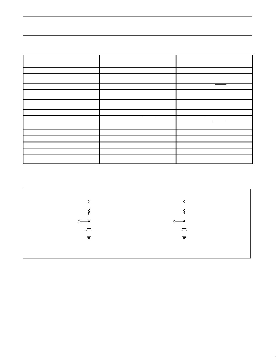
AC LOAD CONDITIONS
CL = 150pF
NOTES:
Open-drain outputs.
CL = Load capacitance includes JIG and probe capacitance.
2.2V
OUTPUT
750
CL = 50pF
+5V
OUTPUT
2k
SD00080

Philips Semiconductors
Product specification
SCN2661/SCN68661
Enhanced programmable communications
interface (EPCI)
1994 Apr 27
14
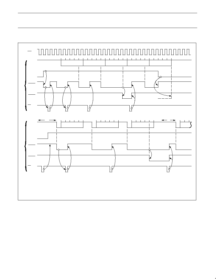
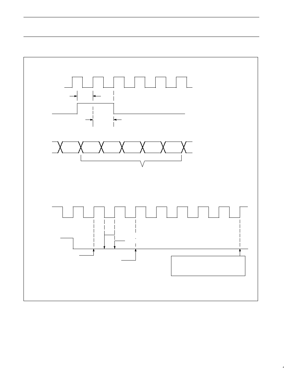
TIMING DIAGRAMS
RESET
tRES
RESET
BRCLK,
TxC, RxC
1/fBRG
tR/TH
tBRH
tR/TL
tBRL
1/fR/T
CLOCK
TRANSMIT
RECEIVE
TxC
(INPUT)
1 BIT TIME
(1, 16, OR 64 CLOCK PERIODS)
TxD
TxC
(OUTPUT)
tTxD
tTCS
tTxD
RxD
RxC (IX)
tRXS
tRXH
tCE
tCED
CE
A0
,
A1
R/W
tAS
tCS
tAH
tCH
D0�D7
(WRITE)
tDS
tDH
BUS
FLOATING
NOT
VALID
BUS
FLOATING
DATA VALID
tDD
tDF
D0�D7
(READ)
READ AND WRITE
SD00052
Philips Semiconductors
Product specification
SCN2661/SCN68661
Enhanced programmable communications
interface (EPCI)
1994 Apr 27
15
TIMING DIAGRAMS (Continued)
1
2
3
4
5
DATA 1
1
2
3
4
5
DATA 2
1
2
3
4
5
DATA 3
1
2
3
4
5
SYN 1
1
2
3
4
5
DATA 4
1
2
3
4
5
DATA 1
A
B
C
1
2
3
4
5
A
B
C
DATA 2
1
2
3
4
5
A
B
C
DATA 3
1
2
A
DATA 4
D
D
DATA 1
DATA 2
DATA 3
DATA 4
DATA 1
DATA 2
DATA 3
DATA 4
TxC (1X)
TxD
TxEN
TxRDY
TxEMT
CE FOR
WRITE
OF THR
TxD
TxEN
TxRDY
TxEMT
CE FOR
WRITE
OF THR
ASYNCHRONOUS MODE
SYNCHRONOUS MODE
TxRDY, TxEMT (Shown for 5-bit characters, no parity, 2 stop bits [in asynchronous mode])
NOTES:
A = Start bit
B = Stop bit 1
C = Stop bit 2
D = TxD marking condition
TxEMT goes low at the beginning of the last data bit, or, if parity is enabled, at the beginning of the parity bit.
SD00053
Philips Semiconductors
Product specification
SCN2661/SCN68661
Enhanced programmable communications
interface (EPCI)
1994 Apr 27
16
TIMING DIAGRAMS (Continued)
SD00081
tes
tH
1X RxC
XSYNC
RxD
RxC + 16 OR 64
RxD
X
0
1
2
3
4
CHARACTER ASSEMBLY
EXTERNAL SYNCHRONIZATION WITH XSYNC
t
es = XSYNC SETUP TIME = 300ns
t
H = XSYNC HOLD TIME = ONE RxC
BREAK DETECTION TIMING
MISSING STOP BIT
DETECTED SET FE BIT*
1st DATA BIT
SAMPLED
LOOK FOR START BIT = LOW (IF RxD IS HIGH, LOOK FOR HIGH TO LOW TRANSITION)
FALSE START BIT CHECK MADE (RxD LOW)
Rx CHARACTER = 5 BITS, NO PARITY
MISSING STOP BIT DETECTED, SET FE BIT.
0
RHR, ACTIVATE RxRDY. SET BKDET PIN
RxD
INPUT RxSR UNTIL A MARK TO SPACE
TRANSITION OCCURS.
NOTE:
* If the stop bit is present, the start bit search will commence immediately.
Philips Semiconductors
Product specification
SCN2661/SCN68661
Enhanced programmable communications
interface (EPCI)
1994 Apr 27
17
TIMING DIAGRAMS (Continued)
1
2
3
4
5
SYN 1
1
2
3
4
5
DATA 1
1
2
3
4
5
DATA 2
1
2
3
4
5
DATA 3
1
2
3
4
5
DATA 4
1
2
3
4
5
DATA 1
A
B
C
1
2
3
4
5
A
B
C
DATA 2
1
2
3
4
5
A
DATA 3
D
READ RHR
(DATA 1)
READ RHR
(DATA 3)
READ
STATUS
RxC
RxD
RxEN
RxRDY
CE FOR
READ
RxD
RxEN
RxRDY
CE FOR
READ
ASYNCHRONOUS MODE
SYNCHRONOUS MODE
RxRDY (Shown for 5-bit characters, no parity, 2 stop bits [in asynchronous mode])
NOTES:
A = Start bit
B = Stop bit 1
C = Stop bit 2
D = TxD marking condition
1
2
3
4
5
DATA 5
IGNORED
READ RHR
(DATA 1)
READ RHR
(DATA 2)
READ RHR
(DATA 3)
READ RHR
(DATA 3)
READ
STATUS
SYNDET
STATUS BIT
D
_
_
B
C
1
2
3
A
DATA 4
OVERRUN
STATUS BIT
SD00054

Philips Semiconductors
Product specification
SCN2661/SCN68661
Enhanced programmable communications
interface (EPCI)
1994 Apr 27
18
TYPICAL APPLICATIONS
SD00082
ADDRESS BUS
CONTROL BUS
DATA BUS
8
RxD
TxD
BRCLK
SCN2661/68661
EIA TO TTL
CONVERT
(OPT)
BAUD RATE CLOCK
OSCILLATOR
ASYNCHRONOUS INTERFACE TO CRT TERMINAL
CRT
TERMINAL
ADDRESS BUS
CONTROL BUS
DATA BUS
8
RxD
TxD
SCN2661/68661
ASYNCHRONOUS INTERFACE TO TELEPHONE LINES
DSR
DTR
CTS
RTS
DCD
BRCLK
ASYNC
MODEM
BAUD RATE CLOCK
OSCILLATOR
PHONE
LINE
INTERFACE
TELEPHONE
LINE
Philips Semiconductors
Product specification
SCN2661/SCN68661
Enhanced programmable communications
interface (EPCI)
1994 Apr 27
19
TYPICAL APPLICATIONS (Continued)
ADDRESS BUS
CONTROL BUS
DATA BUS
RxD
TxD
SCN2661/68661
SYNCHRONOUS
TERMINAL OR
PERIPHERAL
DEVICE
SYNCHRONOUS INTERFACE TO TERMINAL OR PERIPHERAL DEVICE
ADDRESS BUS
CONTROL BUS
DATA BUS
RxD
TxD
SCN2661/68661
SYNCHRONOUS INTERFACE TO TELEPHONE LINES
DCD
RTS
DSR
DTR
SYNC
MODEM
PHONE
LINE
INTERFACE
TELEPHONE
LINE
RxC
TxC
RxC
TxC
CTS
SD00083