 | –≠–ª–µ–∫—Ç—Ä–æ–Ω–Ω—ã–π –∫–æ–º–ø–æ–Ω–µ–Ω—Ç: SE98PW | –°–∫–∞—á–∞—Ç—å:  PDF PDF  ZIP ZIP |

1.
General description
The SE98 is a JEDEC compliant local temperature sensor specifically designed for higher
performance SO-DIMM applications. The temperature sensor is mounted on the
SO-DIMM module and communicates with the processor via the I
2
C-bus/SMBus. Since
the DRAM refresh rate is dependent on temperature, mounting the temperature sensor on
the module allows the processor to adjust the refresh rate based on the actual
temperature instead of the calculated worst-case temperature. The end result being
longer battery life and better system performance.
The SE98 consists of a
A-D converter that continuously monitors and updates its own
temperature readings, converts the reading to digital data, and registers into the data
temperature register. The data is compared to three alarm registers which are
programmed and read via a 2-wire serial bus (SMBus, I
2
C-bus Standard-mode and
I
2
C-bus Fast-mode). The device also supports the SMBus time-out function that prevents
system lock-ups.
SO-DIMM applications normally use the C-grade accuracy SE98TK temperature sensor.
For applications requiring higher B-grade accuracy, the SE98TK/1 is available.
2.
Features
I
Monitor local temperature
I
JEDEC (JC-42.4) SO-DIMM temperature sensor compliant
I
Local temperature sensor accuracy (V
DD
= 3.3 V
±
10 %):
N
75
∞
C to 95
∞
C--sensor grade B =
±
1
∞
C; sensor grade C =
±
2.0
∞
C
N
40
∞
C to 125
∞
C--sensor grade B =
±
2
∞
C; sensor grade C =
±
3
∞
C
N
≠20
∞
C to 125
∞
C--sensor grade B =
±
3
∞
C; sensor grade C =
±
4
∞
C
I
ADC resolution: 0.125
∞
C
I
Conversion rate: 8 Hz minimum
I
Programmable hysteresis threshold: 0
∞
C, 1.5
∞
C, 3
∞
C, 6
∞
C
I
Over/under/critical temperature EVENT output
I
Security lock bit for data protection
I
Operating voltage range: 3.0 V to 3.6 V
I
Maximum operating current: 250
µ
A
I
Maximum standby current is 15
µ
A
I
I
2
C-bus and SMBus compatible, supporting:
N
Bus speed: 0 Hz to 400 kHz
N
SMBus Alert and Time-out (programmable)
I
Operating temperature range: ≠20
∞
C to +125
∞
C
SE98
SO-DIMM SMBus/I
2
C-bus temperature sensor
Rev. 01 -- 10 May 2006
Product data sheet
SE98_1
© Koninklijke Philips Electronics N.V. 2006. All rights reserved.
Product data sheet
Rev. 01 -- 10 May 2006
2 of 28
Philips Semiconductors
SE98
SO-DIMM SMBus/I
2
C-bus temperature sensor
I
Offered in TSSOP8 and HVSON8 packages
3.
Applications
I
Memory module
I
Notebook, desktop, server
I
Enterprise networking
4.
Ordering information
5.
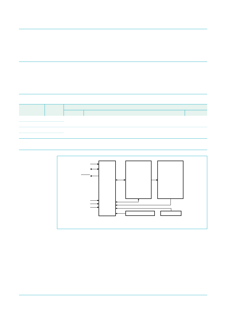
Block diagram
Table 1.
Ordering information
Type number
Topside
mark
Package
Name
Description
Version
SE98PW
SE98
TSSOP8
plastic thin shrink small outline package; 8 leads;
body width 4.4 mm
SOT530-1
SE98PW/1
98/1
SE98TK
SE98
HVSON8
plastic thermal enhanced very thin small outline package;
no leads; 8 terminals; body 3
◊
3
◊
0.85 mm
SOT908-1
SE98TK/1
S98/1
Fig 1.
Block diagram of SE98
002aab280
SMBus
INTERFACE
SCL
A0
A1
A2
SDA
EVENT
CONTROL
AND
STATUS
REGISTER
TEMPERATURE
SENSOR
DEVICE I.D.
MANUFACTURER I.D.
SE98_1
© Koninklijke Philips Electronics N.V. 2006. All rights reserved.
Product data sheet
Rev. 01 -- 10 May 2006
3 of 28
Philips Semiconductors
SE98
SO-DIMM SMBus/I
2
C-bus temperature sensor
6.
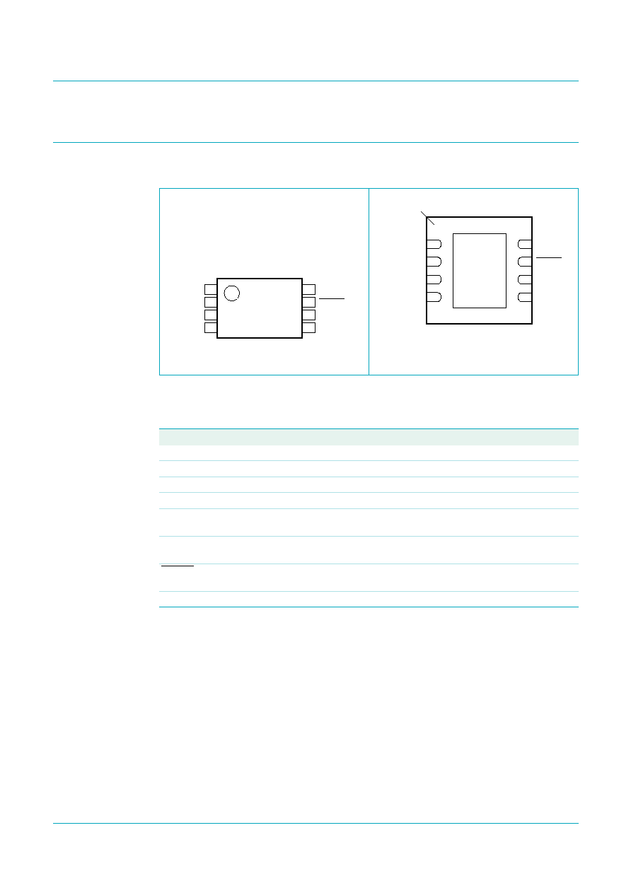
Pinning information
6.1 Pinning
6.2 Pin description
Fig 2.
Pin configuration for TSSOP8
Fig 3.
Pin configuration for HVSON8
SE98PW
SE98PW/1
A0
V
CC
A1
EVENT
A2
SCL
GND
SDA
002aab806
1
2
3
4
6
5
8
7
Transparent top view
5
4
6
3
7
2
8
1
terminal 1
index area
002aab804
SE98TK
SE98TK/1
SDA
A2
GND
SCL
A1
EVENT
A0
V
CC
Table 2.
Pin description
Symbol
Pin
Type
Description
A0
1
I
I
2
C-bus/SMBus slave address bit 0
A1
2
I
I
2
C-bus/SMBus slave address bit 1
A2
3
I
I
2
C-bus/SMBus slave address bit 2
GND
4
ground
device ground
SDA
5
I/O
SMBus/I
2
C-bus serial data input/output (open-drain).
Must have external pull-up resistor.
SCL
6
I
SMBus/I
2
C-bus serial clock input/output (open-drain).
Must have external pull-up resistor.
EVENT
7
O
Thermal alarm output for high/low and critical temperature
limit (open-drain). Must have external pull-up resistor.
V
CC
8
power
device power supply (3.0 V to 3.6 V)
SE98_1
© Koninklijke Philips Electronics N.V. 2006. All rights reserved.
Product data sheet
Rev. 01 -- 10 May 2006
4 of 28
Philips Semiconductors
SE98
SO-DIMM SMBus/I
2
C-bus temperature sensor
7.
Functional description
7.1 Serial bus interface
The SE98 uses the 2-wire serial bus (I
2
C-bus/SMBus) to communicate with a host
controller. The serial bus consists of a clock (SCL) and data (SDA) signals. The device
can operate on either the I
2
C-bus Standard/Fast mode or SMBus. The I
2
C-bus Standard
mode is defined to have bus speeds from 0 Hz to 100 kHz, I
2
C-bus Fast mode from 0 Hz
to 400 kHz, and the SMBus is from 10 kHz to 100 kHz. The host or bus master generates
the SCL signal, and the SE98 uses the SCL signal to receive or send data on the SDA
line. Data transfer is serial, bidirectional, and is one bit at a time with the Most Significant
Bit (MSB) transferred first, and a complete I
2
C-bus data is 1 byte. Since SCL and SDA are
open-drain, pull-up resistors must be installed on these pins.
7.2 Slave address
The SE98 uses a 4-bit fixed and 3-bit programmable (A0, A1 and A2) 7-bit slave address
that allows a total of eight devices to co-exist on the same bus. The input of each pin is
sampled at the start of each I
2
C-bus/SMBus access. The temperature sensor's fixed
address is 0011.
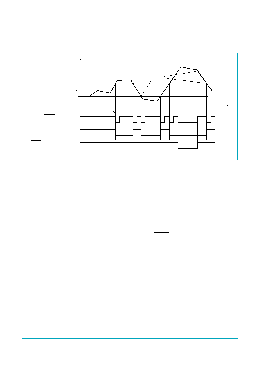
7.3 EVENT output
The EVENT pin is an open-drain output whose function can be programmed as an
interrupt, comparator, or critical alarm mode. When the device operates in Interrupt mode,
and the temperature reaches a critical temperature, the device switches to the comparator
mode automatically and asserts the EVENT pin. When the temperature drops below
critical temperature, the device reverts back to either interrupt or comparator mode, as
programmed in the Configuration Register. The interrupt latch can be cleared by writing a
`1' to the `clear EVENT' bit in the Configuration Register or by performing the SMBus Alert
Response Address (ARA).
In comparator mode, the EVENT pin remains asserted until the temperature falls below
the value programmed in the Upper Boundary Alarm Trip Register or rises above the
value programmed in the Lower Boundary Alarm Trip register, or until the range of these
alarm registers are reprogrammed and the temperature falls inside the alarm limits.
Figure 5
depicts the EVENT output for all the three modes. All event thresholds use
hysteresis as programmed in the Configuration Register.
Fig 4.
Slave address
R/W
002aab304
0
0
1
1
A2
A1
A0
fixed
hardware
selectable
slave address
MSB
LSB
X
SE98_1
© Koninklijke Philips Electronics N.V. 2006. All rights reserved.
Product data sheet
Rev. 01 -- 10 May 2006
5 of 28
Philips Semiconductors
SE98
SO-DIMM SMBus/I
2
C-bus temperature sensor
7.3.1 Alarm window
The alarm window consists of two registers: an Upper Boundary Alarm Trip register (02h),
and a Lower Boundary Alarm Trip register (03h). The Upper Boundary Alarm Trip register
holds the upper temperature trip point, while the Lower Boundary Alarm Trip register holds
the lower temperature trip point. When the EVENT control is enabled, the EVENT output
will be triggered whenever entering or exiting the alarm window.
7.3.2 Critical trip
The device can be programmed in such a way that the EVENT output is triggered when
the temperature exceeds the critical trip point set by the Critical Alarm Trip register (04h).
When the temperature sensor reaches the critical temperature value, the device is
automatically placed in comparator mode; the EVENT output is only cleared when the
temperature falls below the critical temperature value and cannot be cleared through the
clear EVENT bit or SMBus Alert.
7.4 Conversion rate
The conversion time is the amount of time required for the ADC to complete a temperature
measurement for the local temperature sensor. The conversion rate is the inverse of the
conversion period which describes the number of cycles the temperature measurement
completes in one second--the faster the conversion rate, the faster the temperature
reading is updated. The SE98's conversion rate is at least 8 Hz or 125 ms.
Fig 5.
EVENT output for `Interrupt', `Comparator', and `Critical Temp only' modes
002aab233
time
temperature (
∞
C)
critical
EVENT in Interrupt mode
EVENT in Comparator mode
EVENT in `Critical Temp only' mode
alarm window
hysteresis affects
these trip points
software clears event
Lower Boundary Alarm
Upper Boundary Alarm

SE98_1
© Koninklijke Philips Electronics N.V. 2006. All rights reserved.
Product data sheet
Rev. 01 -- 10 May 2006
6 of 28
Philips Semiconductors
SE98
SO-DIMM SMBus/I
2
C-bus temperature sensor
7.5 Power-up default condition
After power-on, the SE98 is initialized to the following default condition:
∑
Starts monitoring local sensor
∑
EVENT register is cleared--EVENT output is pulled HIGH by external pull-ups
∑
EVENT hysteresis is defaulted to 0
∞
C
∑
Command pointer is defaulted to `00h'
∑
Critical Temp, Alarm Temperature Upper and Lower Boundary Trip register are
defaulted to 0
∞
C
∑
Operational mode: comparator
7.6 SMBus Time-out
The SE98 supports SMBus time-out feature. If the host holds SCL LOW between 25 ms
and 35 ms, the SE98 would reset its internal state machine to the bus IDLE state to
prevent the system bus hang-up. This feature is turned on by default. The SMBus time-out
is disabled by writing a logic 1 to bit 7 of register 22h.
Remark: When SMBus time-out is enabled, the I
2
C-bus minimum bus speed is limited by
the SMBus time-out timer, and goes down to only 10 kHz.
7.7 SMBus Alert
The SE98 supports SMBus Alert when it is programmed for the Interrupt mode and when
the EVENT polarity bit is set to logic 0. The EVENT pin can be ANDed with other EVENT
or ALERT signals from other slave devices to signal their intention to communicate with
the host controller. When the host detects EVENT or ALERT signal LOW, it issues an
Alert Response Address (ARA) to which a slave device would respond with its address.
When there are multiple slave devices generating an Alert the SE98 performs bus
arbitration. If it wins the bus, it responds to the ARA and then clears the EVENT pin.
Remark: Either in comparator mode or when the SE98 crosses the critical temperature,
the host must also read the EVENT status bit and provide remedy to the situation by
bringing the temperature to within the alarm window or below the critical temperature if
that bit is set. Otherwise, the EVENT pin will not get de-asserted.
Fig 6.
How SE98 responds to SMBus Alert
0
0
0
1
1
A2
Alert Response Address
1
1
0
0
S
0
0
0
START bit
read
acknowledge
002aab330
A1
A0
0
1
P
device address
not acknowledge
STOP bit
host NACK and
sends a STOP bit
Slave acknowledges and
sends its slave address.
The last bit of slave address
is hard coded '0'.
master sends a START bit,
ARA and a read command
host detects
SMBus ALERT
1
SE98_1
© Koninklijke Philips Electronics N.V. 2006. All rights reserved.
Product data sheet
Rev. 01 -- 10 May 2006
7 of 28
Philips Semiconductors
SE98
SO-DIMM SMBus/I
2
C-bus temperature sensor
7.8 SMBus/I
2
C-bus interface
The data registers in this device are selected by the Pointer Register. At power-up, the
Pointer Register is set to `00', the location for the Capability Register. The Pointer Register
latches the last location is was set to. Each data register falls into one of three types of
user accessibility:
∑
Read only
∑
Write only
∑
Write/Read same address.
A `write' to this device will always include the address byte and the pointer byte. A write to
any register other than the Pointer register requires two data bytes.
Reading this device can take place either of two ways:
∑
If the location latched in the Pointer Register is correct (most of the time it is expected
that the Pointer Register will point to one of the Temperature Register (as it will be the
data most frequently read), then the read can simply consist of an address byte,
followed by retrieving the two data bytes.
∑
If the Pointer Register needs to be set, then an address byte, pointer byte,
repeat START, and another address byte will accomplish a read.
The data byte has the most significant bit first. At the end of a read, this device can accept
either Acknowledge (ACK) or No Acknowledge (NACK) from the Master (No Acknowledge
is typically used as a signal for the slave that the Master has read its last byte). It takes this
device 125 ms to measure the temperature. Refer to the following timing diagrams on how
to program the device.
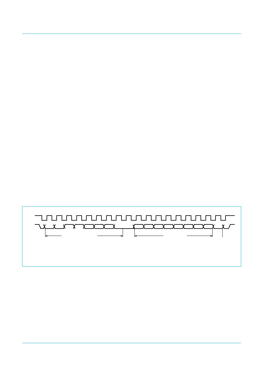
A = ACK = Acknowledge bit. W = Write bit = 0. R = Read bit = 1.
Fig 7.
SMBus/I
2
C-bus write to the Pointer Register
1
2
3
4
5
6
7
8
9
1
2
3
4
5
6
7
8
9
SCL
A6
A5
A4
A3
A2
A1
A0
SDA
D7
D6
D5
D4
D3
D2
D1
D0
device address and write
register address
W
A
S
START
by host
ACK
by
device
P
STOP
by host
A
ACK
by
device
002aab308

SE98_1
© Koninklijke Philips Electronics N.V. 2006. All rights reserved.
Product data sheet
Rev. 01 -- 10 May 2006
8 of 28
Philips Semiconductors
SE98
SO-DIMM SMBus/I
2
C-bus temperature sensor
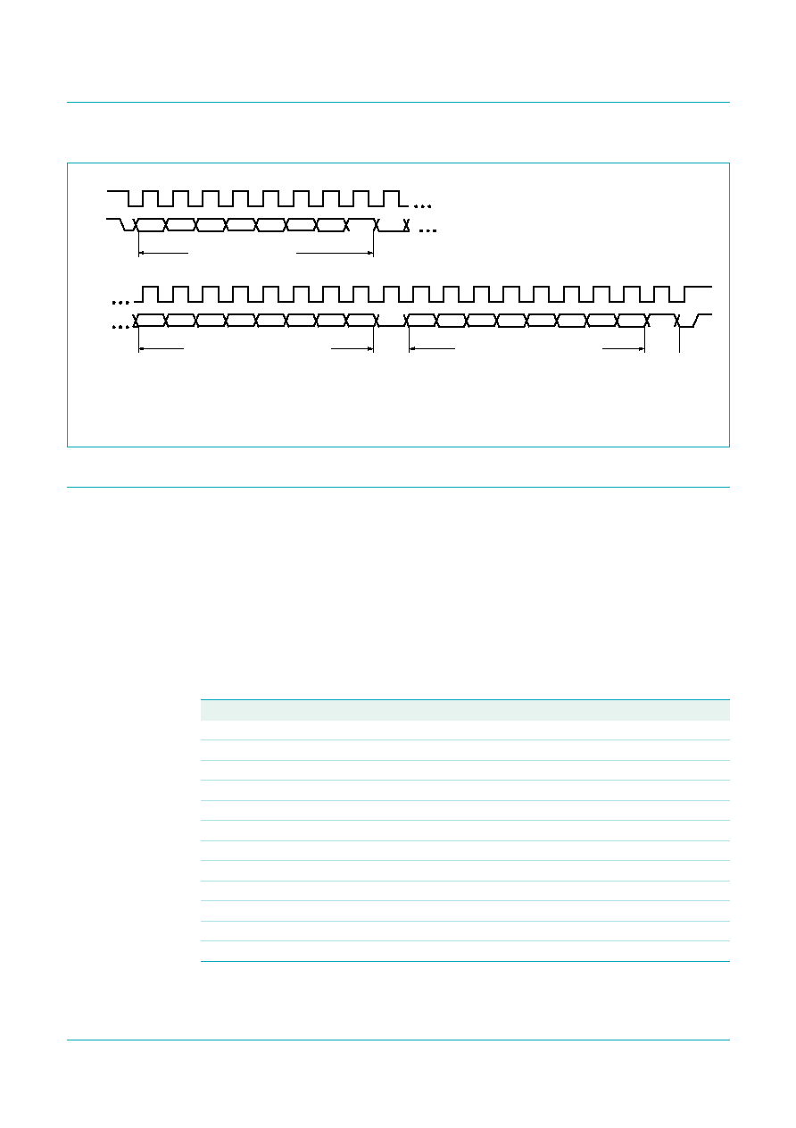
A = ACK = Acknowledge bit. W = Write bit = 0. R = Read bit = 1.
Fig 8.
SMBus/I
2
C-bus write to the Pointer Register followed by a write data word
1
2
3
4
5
6
7
8
9
1
2
3
4
5
6
7
8
9
SCL
A6
A5
A4
A3
A2
A1
A0
SDA
D7
D6
D5
D4
D3
D2
D1
D0
device address and write
write register address
W
A
S
START
by host
ACK
by device
A
ACK
by device
(cont.)
(cont.)
002aab412
1
2
3
4
5
6
7
8
9
1
2
3
4
5
6
7
8
9
SCL
D15
D14
D13
D12
D11
D10
D9
SDA
D7
D6
D5
D4
D3
D2
D1
D0
most significant byte data
least significant byte data
A
by host
ACK
by device
P
STOP
by host
D8
A
ACK
by device
A = ACK = Acknowledge bit. NA = Not Acknowledge bit. W = Write bit = 0. R = Read bit = 1.
Fig 9.
SMBus/I
2
C-bus write to Pointer Register followed by a repeat START and an immediate data word read
1
2
3
4
5
6
7
8
9
1
2
3
4
5
6
7
8
9
SCL
A6
A5
A4
A3
A2
A1
A0
SDA
D7
D6
D5
D4
D3
D2
D1
D0
device address and write
read register address
W
A
S
START
by host
ACK
by device
A
ACK
by device
(cont.)
(cont.)
1
2
3
4
5
6
7
8
9
D15
D14
D13
D12
D11
D10
D9
D8
returned most significant byte data
A
ACK
by host
SCL
SDA
1
2
3
4
5
6
7
8
9
SCL
A6
A5
A4
A3
A2
A1
A0
SDA
device address and read
R
A
SR
repeated
START
by host
ACK
by device
(cont.)
(cont.)
002aab413
1
2
3
4
5
6
7
8
9
D7
D6
D5
D4
D3
D2
D1
D0
returned least significant byte data
P
STOP
by host
NA
NACK
by host
SE98_1
© Koninklijke Philips Electronics N.V. 2006. All rights reserved.
Product data sheet
Rev. 01 -- 10 May 2006
9 of 28
Philips Semiconductors
SE98
SO-DIMM SMBus/I
2
C-bus temperature sensor
8.
Register descriptions
8.1 Register overview
This section describes all the registers used in the SE98. The registers are used for
latching the temperature reading, storing the low and high temperature limits, configuring,
the hysteresis threshold and the ADC, as well as reporting status. The device uses the
pointer register to access these registers. Read registers, as the name implies, are used
for read only, and the write registers are for write only. Any attempt to read from a
write-only register will result in reading zeroes. Writing to a read-only register will have no
effect on the read even though the write command is acknowledged. The Pointer register
is an 8-bit register. All other registers are 16-bit.
A write to reserved registers my cause unexpected results which may result in requiring a
reset by removing and re-applying its power.
A = ACK = Acknowledge bit. NA = Not Acknowledge bit. W = Write bit = 0. R = Read bit = 1.
Fig 10. SMBus/I
2
C-bus word read from register with a pre-set pointer
1
2
3
4
5
6
7
8
9
D15
D14
D13
D12
D11
D10
D9
D8
returned most significant byte data
A
ACK
by host
SCL
SDA
1
2
3
4
5
6
7
8
9
SCL
A6
A5
A4
A3
A2
A1
A0
SDA
device address and read
R
A
ACK
by device
(cont.)
(cont.)
002aab414
1
2
3
4
5
6
7
8
9
D7
D6
D5
D4
D3
D2
D1
D0
returned least significant byte data
P
STOP
NA
NACK
by host
S
START
by host
Table 3.
Register summary
Address (hex)
POR state (hex)
Register name
n/a
n/a
Pointer Register
00h
0015h/0017h
Capability Register (B-grade = 0017h, C-grade = 0015h)
01h
0000h
Configuration Register
02h
0000h
Upper Boundary Alarm Trip Register
03h
0000h
Lower Boundary Alarm Trip Register
04h
0000h
Critical Alarm Trip Register
05h
n/a
Temperature Register
06h
1131h
Manufacturer ID Register
07h
A101h
Device ID/Revision Register
08h to 21h
0000h
reserved registers
22h
0000h
SMBus Register
23h to FFh
0000h
reserved registers

SE98_1
© Koninklijke Philips Electronics N.V. 2006. All rights reserved.
Product data sheet
Rev. 01 -- 10 May 2006
10 of 28
Philips Semiconductors
SE98
SO-DIMM SMBus/I
2
C-bus temperature sensor
8.2 Capability Register (00h, 16-bit read-only)
[1]
See
Table 5
.
Table 4.
Capability Register (address 00h) bit allocation
Bit
15
14
13
12
11
10
9
8
Symbol
RFU
Reset
0
0
0
0
0
0
0
0
Access
R
R
R
R
R
R
R
R
Bit
7
6
5
4
3
2
1
0
Symbol
RFU
TRES
WRNG
HACC
BCAP
Reset
0
0
0
1
0
1
[1]
1
Access
R
R
R
R
R
R
R
R
Table 5.
Capability Register (address 00h) bit description
Bit
Symbol
Description
15:5
RFU
Reserved for future use. Must be zero.
4:3
TRES
Temperature resolution.
10 -- 0.125
∞
C LSB
2
WRNG
Wider range.
1 -- can read temperatures below 0
∞
C and set sign bit accordingly
1
HACC
Higher accuracy.
0 -- Accuracy
±
2
∞
C over the active range and
±
3
∞
C over the
monitor range (C-grade)
1 -- High accuracy
±
1
∞
C over the active range and
±
2
∞
C over the
monitor range (B-grade)
0
BCAP
Basic capability.
1 -- Has Alarm and Critical Trips capability.

SE98_1
© Koninklijke Philips Electronics N.V. 2006. All rights reserved.
Product data sheet
Rev. 01 -- 10 May 2006
11 of 28
Philips Semiconductors
SE98
SO-DIMM SMBus/I
2
C-bus temperature sensor
8.3 Configuration Register (01h, 16-bit read/write)
Table 6.
Configuration Register (address 01h) bit allocation
Bit
15
14
13
12
11
10
9
8
Symbol
RFU
HEN
SHMD
Reset
0
0
0
0
0
0
0
0
Access
R
R
R
R
R
R/W
R/W
R/W
Bit
7
6
5
4
3
2
1
0
Symbol
CTLB
AWLB
CEVNT
ESTAT
EOCTL
CVO
EP
EMD
Reset
0
0
0
0
0
0
0
0
Access
R/W
R/W
R/W
R/W
R/W
R/W
R/W
R/W
Table 7.
Configuration Register (address 01h) bit description
Bit
Symbol
Description
15:11
RFU
reserved for future use; must be `0'.
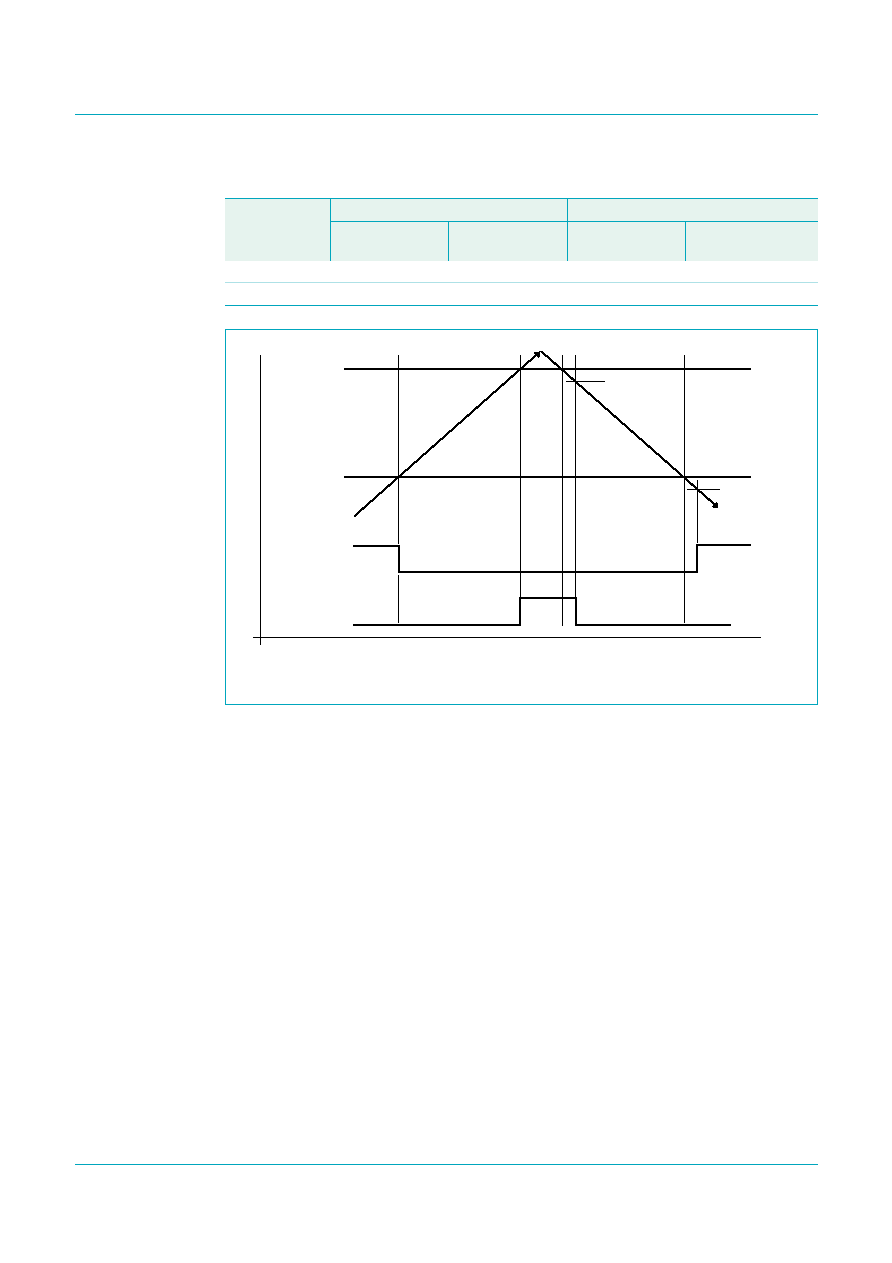
10:9
HEN
Hysteresis Enable
00 -- Disable hysteresis (default)
01 -- Enable hysteresis at 1.5
∞
C
10 -- Enable hysteresis at 3
∞
C
11 -- Enable hysteresis at 6
∞
C
When enabled, hysteresis is applied to temperature movement around
trigger points. For example, consider the behavior of the `Above Alarm
Window' bit (bit 14 of the Temperature register) when the hysteresis is set
to 3
∞
C. As the temperature rises, bit 14 will be set to 1 (temperature is
above the alarm window) when the Temperature register contains a value
that is greater than the value in the Alarm Temperature Upper Boundary
Register. If the temperature decreases, bit 14 will remain set until the
measured temperature is less than or equal to the value in the Alarm
Temperature Upper Boundary register minus 3
∞
C. (Refer to
Figure 5
and
Table 8
).
Similarly, the `Below Alarm Window' bit (bit 13 of the Temperature register)
will be set to 0 (temperature is equal to or above the Alarm Window Lower
Boundary Trip Register) when the value in the Temperature register is
equal to or greater than the value in the Alarm Temperature Lower
Boundary Register. As the temperature decreases, bit 13 will be set to 1
when the value in the Temperature Register is equal to or less than the
value in the Alarm Temperature Lower Boundary Register minus 3
∞
C.
Note that hysteresis is also applied to EVENT pin functionality.
When either of the lock bits is set, these bits cannot be altered.
8
SHMD
Shutdown Mode.
0 -- Enabled Temperature Sensor (default)
1 -- Disabled Temperature Sensor
When shut down, the thermal sensor diode and A/D converter are
disabled to save power, no events will be generated. When either of the
lock bits is set, this bit cannot be set until unlocked. However, it can be
cleared at any time.

SE98_1
© Koninklijke Philips Electronics N.V. 2006. All rights reserved.
Product data sheet
Rev. 01 -- 10 May 2006
12 of 28
Philips Semiconductors
SE98
SO-DIMM SMBus/I
2
C-bus temperature sensor
7
CTLB
Critical Trip Lock bit.
0 -- Critical Alarm Trip Register is not locked and can be altered
(default).
1 -- Critical Alarm Trip Register settings cannot be altered.
This bit is initially cleared. When set, this bit will return a 1, and remains
locked until cleared by internal Power-on reset. This bit can be written with
a single write and do not require double writes.
6
AWLB
Alarm Window Lock bit.
0 -- Upper and Lower Alarm Trip Registers are not locked and can be
altered (default).
1 -- Upper and Lower Alarm Trip Registers setting cannot be altered.
This bit is initially cleared. When set, this bit will return a 1 and remains
locked until cleared by internal power-on reset. This bit can be written with
a single write and does not require double writes.
5
CEVNT
Clear EVENT (write only).
0 -- No effect (default).
1 -- Clears active EVENT in Interrupt mode. Writing to this register has
no effect in Comparator mode.
When read, this register always returns zero.
4
ESTAT
EVENT Status (read only).
0 -- EVENT output condition is not being asserted by this device
(default).
1 -- EVENT output pin is being asserted by this device due to Alarm
Window or Critical Trip condition.
The actual event causing the event can be determined from the Read
Temperature Register. Interrupt Events can be cleared by writing to the
`clear EVENT' bit. Writing to this bit will have no effect.
3
EOCTL
EVENT Output Control.
0 -- EVENT output disabled (default).
1 -- EVENT output enabled.
When either of the lock bits is set, this bit cannot be altered until unlocked.
2
CVO
Critical Event Only.
0 -- EVENT output on Alarm or Critical temperature event (default)
1 -- EVENT only if temperature is above the value in the critical
temperature register
When the alarm window lock bit is set, this bit cannot be altered until
unlocked.
1
EP
EVENT Polarity.
0 -- active LOW (default).
1 -- active HIGH. When either of the alarm or critical lock bits is set, this
bit cannot be altered until unlocked.
0
EMD
EVENT Mode.
0 -- comparator output mode (default)
1 -- interrupt mode
When either of the alarm or critical lock bits is set, this bit cannot be
altered until unlocked.
Table 7.
Configuration Register (address 01h) bit description
...continued
Bit
Symbol
Description
SE98_1
© Koninklijke Philips Electronics N.V. 2006. All rights reserved.
Product data sheet
Rev. 01 -- 10 May 2006
13 of 28
Philips Semiconductors
SE98
SO-DIMM SMBus/I
2
C-bus temperature sensor
Table 8.
Hysteresis Enable
Action
Below Alarm Window Bit (bit 13)
Above Alarm Window Bit (bit 14)
Temperature
slope
Threshold
temperature
Temperature
slope
Temperature
sets
falling
T
th(low)
≠ Hyst
rising
T
th(high)
clears
rising
T
th(low)
falling
T
th(high)
≠ Hyst
Fig 11. Hysteresis timing
002aab415
below
alarm window bit
above
alarm window bit
T
th(high)
≠ Hyst
T
th(low)
≠ Hyst
T
th(high)
T
th(low)
current
temperature
time
temperature

SE98_1
© Koninklijke Philips Electronics N.V. 2006. All rights reserved.
Product data sheet
Rev. 01 -- 10 May 2006
14 of 28
Philips Semiconductors
SE98
SO-DIMM SMBus/I
2
C-bus temperature sensor
8.4 Temperature format
The 16-bit value used in the following Trip Point Set and Temperature Read-Back registers
is 2's complement with the Least Significant Bit (LSB) equal to 0.0625
∞
C. For example:
∑
A value of 019Ch will represent 25.75
∞
C
∑
A value of 07C0h will represent 124
∞
C
∑
A value of 1E64h will represent ≠25.75
∞
C.
The resolution is 0.125
∞
C. The unused LSB (bit 0) is set to `0'. Bit 11 will have a resolution
of 128
∞
C.
The upper 3 bits of the temperature register indicate Trip Status based on the current
temperature, and are not affected by the status of the Event Output.
8.5 Temperature Trip Point registers
8.5.1 Upper Boundary Alarm Trip Register (16-bit read/write)
The value is the upper threshold temperature value for Alarm mode. The data format is
2's complement with bit 2 = 0.25
∞
C. `RFU' bits will always report zero. Interrupts will
respond to the presently programmed boundary values. If boundary values are being
altered in-system, it is advised to turn off interrupts until a known state can be obtained to
avoid superfluous interrupt activity.
Table 9.
Upper Boundary Alarm Trip Register bit allocation
Bit
15
14
13
12
11
10
9
8
Symbol
RFU
SIGN
UBT
Reset
0
0
0
0
0
0
0
0
Access
R
R
R
R/W
R/W
R/W
R/W
R/W
Bit
7
6
5
4
3
2
1
0
Symbol
UBT
RFU
Reset
0
0
0
0
0
0
0
0
Access
R/W
R/W
R/W
R/W
R/W
R/W
R
R
Table 10.
Upper Boundary Alarm Trip Register bit description
Bit
Symbol
Description
15:13
RFU
reserved; always 0
12
SIGN
Sign (MSB)
11:2
UBT
Upper Boundary Alarm Trip Temperature (LSB = 0.25
∞
C)
1:0
RFU
reserved; always 0

SE98_1
© Koninklijke Philips Electronics N.V. 2006. All rights reserved.
Product data sheet
Rev. 01 -- 10 May 2006
15 of 28
Philips Semiconductors
SE98
SO-DIMM SMBus/I
2
C-bus temperature sensor
8.5.2 Lower Boundary Alarm Trip Register (16-bit read/write)
The value is the lower threshold temperature value for Alarm mode. The data format is
2's complement with bit 2 = 0.25
∞
C. RFU bits will always report zero. Interrupts will
respond to the presently programmed boundary values. If boundary values are being
altered in-system, it is advised to turn off interrupts until a known state can be obtained to
avoid superfluous interrupt activity.
8.5.3 Critical Alarm Trip Register (16-bit read/write)
The value is the critical temperature. The data format is 2's complement with
bit 2 = 0.25
∞
C. RFU bits will always report zero.
Table 11.
Lower Boundary Alarm Trip Register bit allocation
Bit
15
14
13
12
11
10
9
8
Symbol
RFU
SIGN
LBT
Reset
0
0
0
0
0
0
0
0
Access
R
R
R
R/W
R/W
R/W
R/W
R/W
Bit
7
6
5
4
3
2
1
0
Symbol
LBT
RFU
Reset
0
0
0
0
0
0
0
0
Access
R/W
R/W
R/W
R/W
R/W
R/W
R
R
Table 12.
Lower Boundary Alarm Trip Register bit description
Bit
Symbol
Description
15:13
RFU
reserved; always 0
12
SIGN
Sign (MSB)
11:2
LBT
Lower Boundary Alarm Trip Temperature (LSB = 0.25
∞
C)
1:0
RFU
reserved; always 0
Table 13.
Lower Boundary Alarm Trip Register bit allocation
Bit
15
14
13
12
11
10
9
8
Symbol
RFU
SIGN
CT
Reset
0
0
0
0
0
0
0
0
Access
R
R
R
R/W
R/W
R/W
R/W
R/W
Bit
7
6
5
4
3
2
1
0
Symbol
CT
RFU
Reset
0
0
0
0
0
0
0
0
Access
R/W
R/W
R/W
R/W
R/W
R/W
R
R
Table 14.
Critical Alarm Trip Register bit description
Bit
Symbol
Description
15:13
RFU
reserved; always 0
12
SIGN
Sign (MSB)
11:2
CT
Critical Alarm Trip Temperature (LSB = 0.25
∞
C)
1:0
RFU
reserved; always 0

SE98_1
© Koninklijke Philips Electronics N.V. 2006. All rights reserved.
Product data sheet
Rev. 01 -- 10 May 2006
16 of 28
Philips Semiconductors
SE98
SO-DIMM SMBus/I
2
C-bus temperature sensor
8.6 Temperature Register (16-bit read-only)
8.7 Manufacturer's ID register (16-bit read-only)
The manufacture's ID matches that assigned to Philips' PCI SIG (1131h), and is intended
for use to identify the manufacturer of the device.
Table 15.
Temperature Register bit allocation
Bit
15
14
13
12
11
10
9
8
Symbol
ACT
AAW
BAW
SIGN
TEMP
Reset
0
0
0
0
0
0
0
0
Access
R
R
R
R
R
R
R
R
Bit
7
6
5
4
3
2
1
0
Symbol
TEMP
RFU
Reset
0
0
0
0
0
0
0
0
Access
R
R
R
R
R
R
R
R
Table 16.
Temperature Register bit description
Bit
Symbol
Description
15
ACT
Above Critical Trip.
0 -- temperature is below the Critical Alarm Trip Register setting
1 -- temperature is equal to or above the Critical Alarm Trip Register
setting
14
AAW
Above Alarm Window.
0 -- temperature is equal to or below the Upper Boundary Alarm Trip
Register
1 -- temperature is above the Alarm window
13
BAW
Below Alarm Window.
0 -- temperature is equal to or above the Lower Boundary Alarm Trip
Register
1 -- temperature is below the Alarm window
12
SIGN
Sign bit.
0 -- positive temperature value
1 -- negative temperature value
11:1
TEMP
Temperature Value (2's complement). (LSB = 0.125
∞
C)
0
RFU
reserved; always 0
Table 17.
Manufacturer's ID register bit allocation
Bit
15
14
13
12
11
10
9
8
Symbol
Manufacturer ID
Reset
0
0
0
1
0
0
0
1
Access
R
R
R
R
R
R
R
R
Bit
7
6
5
4
3
2
1
0
Symbol
(cont.)
Reset
0
0
1
1
0
0
0
1
Access
R
R
R
R
R
R
R
R

SE98_1
© Koninklijke Philips Electronics N.V. 2006. All rights reserved.
Product data sheet
Rev. 01 -- 10 May 2006
17 of 28
Philips Semiconductors
SE98
SO-DIMM SMBus/I
2
C-bus temperature sensor
8.8 Device ID register
The device ID and device revision are A1h and 00h, respectively.
8.9 SMBus Register
Table 18.
Device ID register bit allocation
Bit
15
14
13
12
11
10
9
8
Symbol
Device ID
Reset
1
0
1
0
0
0
0
1
Access
R
R
R
R
R
R
R
R
Bit
7
6
5
4
3
2
1
0
Symbol
Device revision
Reset
0
0
0
0
0
0
0
1
Access
R
R
R
R
R
R
R
R
Table 19.
SMBus Time-out register bit allocation
Bit
15
14
13
12
11
10
9
8
Symbol
RFU
Reset
0
0
0
0
0
0
0
0
Access
R
R
R
R
R
R
R
R
Bit
7
6
5
4
3
2
1
0
Symbol
STMOUT
RFU
SALRT
Reset
0
0
0
0
0
0
0
0
Access
R/W
R
R
R
R
R
R
R/W
Table 20.
SMBus Time-out register bit description
Bit
Symbol
Description
15:8
RFU
reserved; always 0
7
STMOUT
SMBus time-out.
0 -- SMBus time-out is enabled (default)
1 -- disable SMBus time-out
When either of the lock bits is set, this bit cannot be altered until unlocked.
6:1
RFU
reserved; always 0
0
SALRT
SMBus Alert.
0 -- SMBus Alert is enabled (default)
1 -- disable SMBus Alert
When either of the lock bits is set, this bit cannot be altered until unlocked.
SE98_1
© Koninklijke Philips Electronics N.V. 2006. All rights reserved.
Product data sheet
Rev. 01 -- 10 May 2006
18 of 28
Philips Semiconductors
SE98
SO-DIMM SMBus/I
2
C-bus temperature sensor
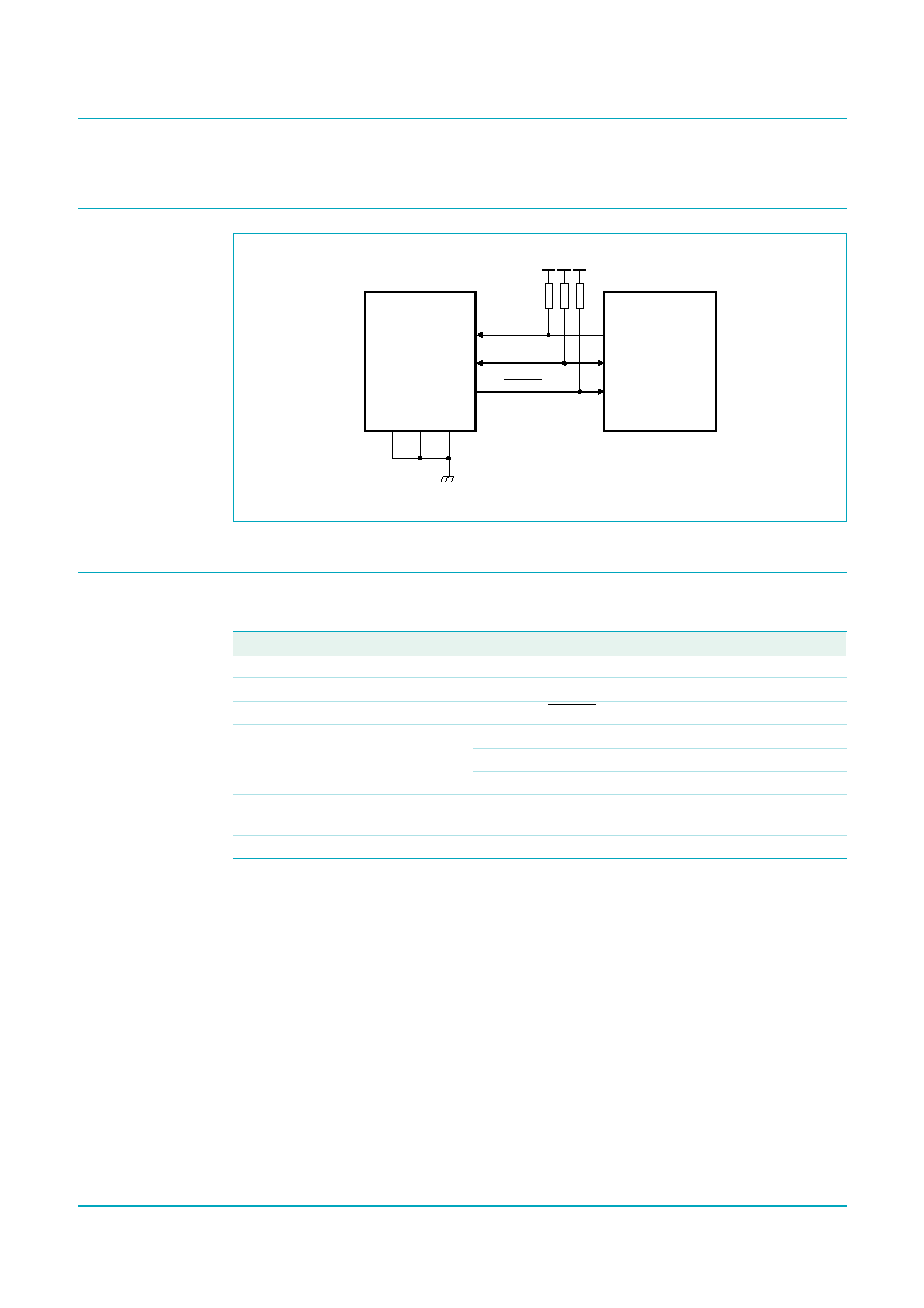
9.
Application design-in information
10. Limiting values
Fig 12. Typical application
002aab282
HOST
CONTROLLER
SE98
A0
A1
A2
SCL
SDA
EVENT
V
DD
10 k
(3
◊
)
Table 21.
Limiting values
In accordance with the Absolute Maximum Rating System (IEC 60134).
Symbol
Parameter
Conditions
Min
Max
Unit
V
DD
supply voltage
≠0.3
+6
V
V
n
voltage on any other pin
≠0.3
+6
V
I
sink
sink current
SDA, SCL, EVENT pins
≠1
50.0
mA
V
esd
electrostatic discharge
voltage
HBM
-
2500
V
MM
-
250
V
CDM
-
1000
V
T
j(max)
maximum junction
temperature
-
150
∞
C
T
stg
storage temperature
≠65
+165
∞
C

SE98_1
© Koninklijke Philips Electronics N.V. 2006. All rights reserved.
Product data sheet
Rev. 01 -- 10 May 2006
19 of 28
Philips Semiconductors
SE98
SO-DIMM SMBus/I
2
C-bus temperature sensor
11. Characteristics
Table 22.
Characteristics
Symbol
Parameter
Conditions
Min
Typ
Max
Unit
T
lim(acc)
temperature limit accuracy
B-grade temperature accuracy;
V
DD
= 3.3 V
±
10 %
T
amb
= 75
∞
C to 95
∞
C
≠1.0
<
±
0.5
+1.0
∞
C
T
amb
= 40
∞
C to 125
∞
C
≠2.0
<
±
1
+2.0
∞
C
T
amb
= ≠20
∞
C to 125
∞
C
≠3.0
<
±
2
+3.0
∞
C
C-grade temperature accuracy;
V
DD
= 3.3 V
±
10 %
T
amb
= 75
∞
C to 95
∞
C
≠2.0
<
±
1
+2.0
∞
C
T
amb
= 40
∞
C to 125
∞
C
≠3.0
<
±
2
+3.0
∞
C
T
amb
= ≠20
∞
C to 125
∞
C
≠4.0
<
±
3
+4.0
∞
C
T
res
temperature resolution
-
0.25
-
∞
C
I
CC(AV)
average supply current
-
-
250
µ
A
I
stb(VCC)
power supply standby
current
SMBus inactive
-
8
15
µ
A
T
conv
conversion period
-
100
-
ms
E
f(conv)
conversion rate error
percentage error in programmed
data
≠30
-
30
%
I
L
leakage current
on A0, A1, A2 pins
-
1
-
µ
A
V
DD
supply voltage
3.0
3.3
3.6
V
Table 23.
SMBus DC characteristics
V
DD
= 3.0 V to 3.6 V; T
amb
= ≠20
∞
C to +120
∞
C; unless otherwise specified. These specifications are guaranteed by design.
Symbol
Parameter
Conditions
Min
Typ
Max
Unit
V
IH
HIGH-level input voltage
SCL, SDA;
V
DD
= 3.0 V to 3.6 V
2.2
-
-
V
V
IL
LOW-level input voltage
SCL, SDA;
V
DD
= 3.0 V to 3.6 V
-
-
0.8
V
I
OL(sink)EVENT_N
LOW-level output sink current on pin
EVENT
V
OL
= 0.4 V
1
-
-
mA
I
OL(sink)(SDA)
LOW-level output sink current on pin
SDA
V
OL
= 0.6 V
6
-
-
mA
I
LOH
HIGH-level output leakage current
V
OH
= V
DD
-
-
1.0
µ
A
I
LIH
HIGH-level input leakage current
V
I
= V
DD
or GND
≠1.0
-
1.0
µ
A
I
LIL
LOW-level input leakage current
V
I
= V
DD
or GND
≠1.0
-
1.0
µ
A
C
i
input capacitance
SCL, SDA pins
-
5
10
pF
SE98_1
© Koninklijke Philips Electronics N.V. 2006. All rights reserved.
Product data sheet
Rev. 01 -- 10 May 2006
20 of 28
Philips Semiconductors
SE98
SO-DIMM SMBus/I
2
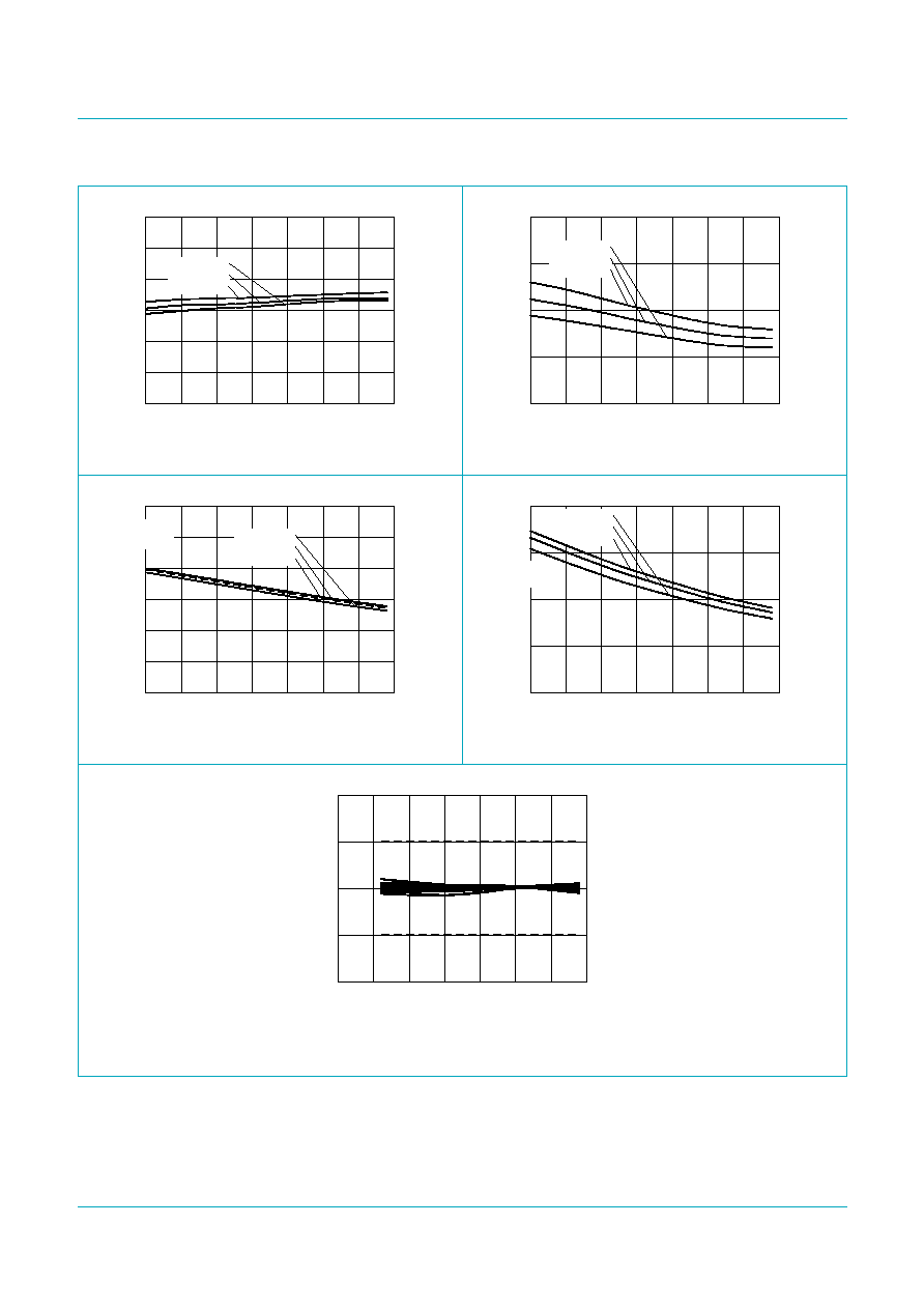
C-bus temperature sensor
Fig 13. Typical I
CC(AV)
Fig 14. Typical I
stb(VCC)
Fig 15. Typical I
OL(sink)EVENT_N
at 0.4 V
Fig 16. Typical I
OL(sink)(SDA)
at 0.6 V
Sample of 25 devices at V
CC
= 3.3 V
Fig 17. Typical Temp Error
100
200
300
I
CC(AV)
(
µ
A)
0
T
amb
(
∞
C)
-
50
125
002aac157
100
75
50
25
0
-
25
V
CC
= 3.0 V
3.3 V
3.6 V
4
16
I
stb(VCC)
(
µ
A)
0
T
amb
(
∞
C)
-
50
125
002aac158
100
75
50
25
0
-
25
V
CC
= 3.0 V
3.3 V
3.6 V
12
8
T
amb
(
∞
C)
-
50
125
002aac159
100
75
50
25
0
-
25
V
CC
= 3.0 V
3.3 V
3.6 V
5.0
10.0
15.0
I
OL(sink)EVENT_N
(mA)
0
T
amb
(
∞
C)
-
50
125
002aac160
100
75
50
25
0
-
25
V
CC
= 3.0 V
3.3 V
3.6 V
15.0
10.0
5.0
20.0
0
I
OL(sink)(SDA)
(mA)
-
2
4
Temp
Error
(
∞
C)
-
4
T
amb
(
∞
C)
-
50
125
002aac161
100
75
50
25
0
-
25
2
0
SE98_1
© Koninklijke Philips Electronics N.V. 2006. All rights reserved.
Product data sheet
Rev. 01 -- 10 May 2006
21 of 28
Philips Semiconductors
SE98
SO-DIMM SMBus/I
2
C-bus temperature sensor
[1]
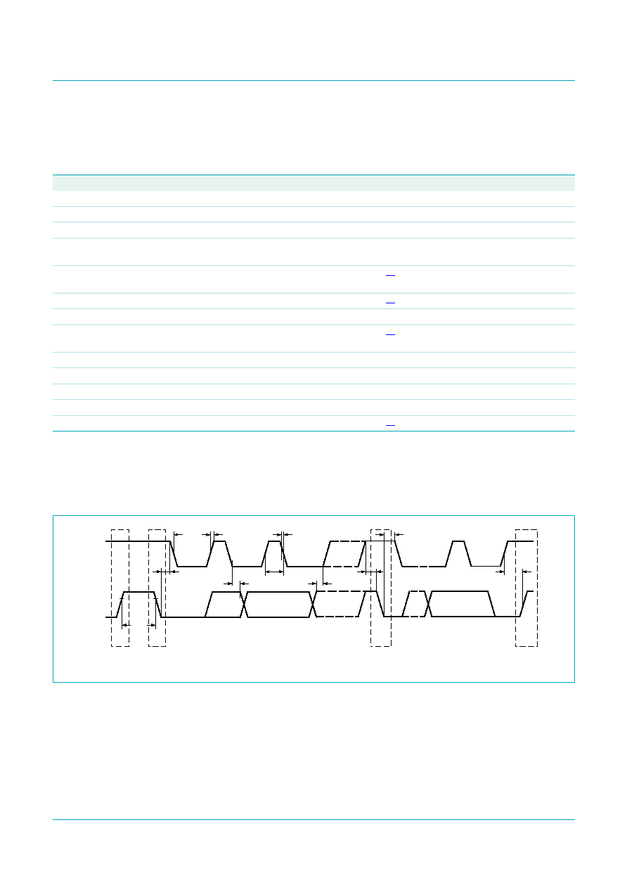
Delay from SDA START to first SCL HIGH-to-LOW transition.
[2]
Delay from SCL HIGH-to-LOW transition to SDA edges.
[3]
Delay from SCL LOW-to-HIGH transition to restart SDA.
[4]
LOW period to reset SMBus.
Table 24.
SMBus AC characteristics
V
DD
= 3.0 V to 3.6 V; T
amb
= ≠20
∞
C to +120
∞
C; unless otherwise specified. These specifications are guaranteed by design.
The AC specifications fully meet or exceed SMBus 2.0 specifications, but allow the bus to interface with the I
2
C-bus from DC
to 400 kHz.
Symbol
Parameter
Conditions
Min
Typ
Max
Unit
f
SCL
SCL clock frequency
0
-
400
kHz
t
LOW
LOW period of the SCL clock
10 % to 10 %
1.3
-
-
µ
s
t
HIGH
HIGH period of the SCL clock
90 % to 90 %
0.6
-
-
µ
s
t
BUF
bus free time between a STOP and
START condition
4.7
-
-
µ
s
t
HD;STA
hold time (repeated) START condition
10 % of SDA to
90 % of SCL
[1]
4.7
-
-
µ
s
t
HD;DAT
data hold time
[2]
300
-
-
ns
t
SU;DAT
data set-up time
250
-
-
ns
t
SU;STA
set-up time for a repeated START
condition
[3]
250
-
-
ns
t
SU;STO
set-up time for STOP condition
0.6
-
-
µ
s
t
r
rise time of both SDA and SCL signals
-
-
300
ns
t
f
fall time of both SDA and SCL signals
-
-
300
ns
t
f(o)
output fall time
-
-
250
ns
t
to(SMBus)
SMBus time-out time
[4]
25
-
35
ms
Fig 18. AC timing diagram
P
S
SCL
SDA
002aab235
S
P
t
LOW
t
r
t
SU;STO
t
HD;STA
t
HD;DAT
t
f
t
BUF
t
SU;DAT
t
SU;STA
t
HIGH
t
HD;STA

SE98_1
© Koninklijke Philips Electronics N.V. 2006. All rights reserved.
Product data sheet
Rev. 01 -- 10 May 2006
22 of 28
Philips Semiconductors
SE98
SO-DIMM SMBus/I
2
C-bus temperature sensor
12. Package outline
Fig 19. Package outline SOT530-1 (TSSOP8)
UNIT
A1
A
max.
A2
A3
bp
L
HE
Lp
w
y
v
c
e
D
(1)
E
(2)
Z
(1)
REFERENCES
OUTLINE
VERSION
EUROPEAN
PROJECTION
ISSUE DATE
IEC
JEDEC
JEITA
mm
0.15
0.05
0.95
0.85
0.30
0.19
0.20
0.13
3.1
2.9
4.5
4.3
0.65
6.5
6.3
0.70
0.35
8
∞
0
∞
0.1
0.1
0.1
0.94
DIMENSIONS (mm are the original dimensions)
Notes
1. Plastic or metal protrusions of 0.15 mm maximum per side are not included.
2. Plastic or metal protrusions of 0.25 mm maximum per side are not included.
0.7
0.5
SOT530-1
MO-153
00-02-24
03-02-18
w
M
bp
D
Z
e
0.25
1
4
8
5
A
A2
A1
Lp
(A3)
detail X
L
HE
E
c
v
M
A
X
A
y
2.5
5 mm
0
scale
TSSOP8: plastic thin shrink small outline package; 8 leads; body width 4.4 mm
SOT530-1
1.1
pin 1 index

SE98_1
© Koninklijke Philips Electronics N.V. 2006. All rights reserved.
Product data sheet
Rev. 01 -- 10 May 2006
23 of 28
Philips Semiconductors
SE98
SO-DIMM SMBus/I
2
C-bus temperature sensor
Fig 20. Package outline SOT908-1 (HVSON8)
0.5
0.2
1
0.05
0.00
A1
Eh
b
UNIT
D
(1)
y
e
1.5
e1
REFERENCES
OUTLINE
VERSION
EUROPEAN
PROJECTION
ISSUE DATE
IEC
JEDEC
JEITA
mm
3.1
2.9
c
Dh
1.65
1.35
y1
3.1
2.9
2.25
1.95
0.3
0.2
0.05
0.1
DIMENSIONS (mm are the original dimensions)
SOT908-1
MO-229
E
(1)
0.5
0.3
L
0.1
v
0.05
w
SOT908-1
HVSON8: plastic thermal enhanced very thin small outline package; no leads;
8 terminals; body 3 x 3 x 0.85 mm
A
(1)
max.
05-09-26
05-10-05
Note
1. Plastic or metal protrusions of 0.075 mm maximum per side are not included.
X
terminal 1
index area
B
A
D
E
detail X
A
A
1
c
C
y
C
y
1
exposed tie bar (4
◊
)
exposed tie bar (4
◊
)
b
terminal 1
index area
e
1
e
A
C
B
v
M
C
w
M
E
h
D
h
L
1
4
5
8
0
1
2 mm
scale

SE98_1
© Koninklijke Philips Electronics N.V. 2006. All rights reserved.
Product data sheet
Rev. 01 -- 10 May 2006
24 of 28
Philips Semiconductors
SE98
SO-DIMM SMBus/I
2
C-bus temperature sensor
13. Soldering
13.1 Introduction to soldering surface mount packages
This text gives a very brief insight to a complex technology. A more in-depth account of
soldering ICs can be found in our
Data Handbook IC26; Integrated Circuit Packages
(document order number 9398 652 90011).
There is no soldering method that is ideal for all surface mount IC packages. Wave
soldering can still be used for certain surface mount ICs, but it is not suitable for fine pitch
SMDs. In these situations reflow soldering is recommended.
13.2 Reflow soldering
Reflow soldering requires solder paste (a suspension of fine solder particles, flux and
binding agent) to be applied to the printed-circuit board by screen printing, stencilling or
pressure-syringe dispensing before package placement. Driven by legislation and
environmental forces the worldwide use of lead-free solder pastes is increasing.
Several methods exist for reflowing; for example, convection or convection/infrared
heating in a conveyor type oven. Throughput times (preheating, soldering and cooling)
vary between 100 seconds and 200 seconds depending on heating method.
Typical reflow peak temperatures range from 215
∞
C to 260
∞
C depending on solder paste
material. The top-surface temperature of the packages should preferably be kept:
∑
below 225
∞
C (SnPb process) or below 245
∞
C (Pb-free process)
≠ for all BGA, HTSSON..T and SSOP..T packages
≠ for packages with a thickness
2.5 mm
≠ for packages with a thickness < 2.5 mm and a volume
350 mm
3
so called
thick/large packages.
∑
below 240
∞
C (SnPb process) or below 260
∞
C (Pb-free process) for packages with a
thickness < 2.5 mm and a volume < 350 mm
3
so called small/thin packages.
Moisture sensitivity precautions, as indicated on packing, must be respected at all times.
13.3 Wave soldering
Conventional single wave soldering is not recommended for surface mount devices
(SMDs) or printed-circuit boards with a high component density, as solder bridging and
non-wetting can present major problems.
To overcome these problems the double-wave soldering method was specifically
developed.
If wave soldering is used the following conditions must be observed for optimal results:
∑
Use a double-wave soldering method comprising a turbulent wave with high upward
pressure followed by a smooth laminar wave.
∑
For packages with leads on two sides and a pitch (e):
≠ larger than or equal to 1.27 mm, the footprint longitudinal axis is preferred to be
parallel to the transport direction of the printed-circuit board;

SE98_1
© Koninklijke Philips Electronics N.V. 2006. All rights reserved.
Product data sheet
Rev. 01 -- 10 May 2006
25 of 28
Philips Semiconductors
SE98
SO-DIMM SMBus/I
2
C-bus temperature sensor
≠ smaller than 1.27 mm, the footprint longitudinal axis must be parallel to the
transport direction of the printed-circuit board.
The footprint must incorporate solder thieves at the downstream end.
∑
For packages with leads on four sides, the footprint must be placed at a 45
∞
angle to
the transport direction of the printed-circuit board. The footprint must incorporate
solder thieves downstream and at the side corners.
During placement and before soldering, the package must be fixed with a droplet of
adhesive. The adhesive can be applied by screen printing, pin transfer or syringe
dispensing. The package can be soldered after the adhesive is cured.
Typical dwell time of the leads in the wave ranges from 3 seconds to 4 seconds at 250
∞
C
or 265
∞
C, depending on solder material applied, SnPb or Pb-free respectively.
A mildly-activated flux will eliminate the need for removal of corrosive residues in most
applications.
13.4 Manual soldering
Fix the component by first soldering two diagonally-opposite end leads. Use a low voltage
(24 V or less) soldering iron applied to the flat part of the lead. Contact time must be
limited to 10 seconds at up to 300
∞
C.
When using a dedicated tool, all other leads can be soldered in one operation within
2 seconds to 5 seconds between 270
∞
C and 320
∞
C.
13.5 Package related soldering information
[1]
For more detailed information on the BGA packages refer to the
(LF)BGA Application Note (AN01026);
order a copy from your Philips Semiconductors sales office.
[2]
All surface mount (SMD) packages are moisture sensitive. Depending upon the moisture content, the
maximum temperature (with respect to time) and body size of the package, there is a risk that internal or
external package cracks may occur due to vaporization of the moisture in them (the so called popcorn
effect). For details, refer to the Drypack information in the
Data Handbook IC26; Integrated Circuit
Packages; Section: Packing Methods.
[3]
These transparent plastic packages are extremely sensitive to reflow soldering conditions and must on no
account be processed through more than one soldering cycle or subjected to infrared reflow soldering with
peak temperature exceeding 217
∞
C
±
10
∞
C measured in the atmosphere of the reflow oven. The package
body peak temperature must be kept as low as possible.
Table 25.
Suitability of surface mount IC packages for wave and reflow soldering methods
Package
[1]
Soldering method
Wave
Reflow
[2]
BGA, HTSSON..T
[3]
, LBGA, LFBGA, SQFP,
SSOP..T
[3]
, TFBGA, VFBGA, XSON
not suitable
suitable
DHVQFN, HBCC, HBGA, HLQFP, HSO, HSOP,
HSQFP, HSSON, HTQFP, HTSSOP, HVQFN,
HVSON, SMS
not suitable
[4]
suitable
PLCC
[5]
, SO, SOJ
suitable
suitable
LQFP, QFP, TQFP
not recommended
[5][6]
suitable
SSOP, TSSOP, VSO, VSSOP
not recommended
[7]
suitable
CWQCCN..L
[8]
, PMFP
[9]
, WQCCN..L
[8]
not suitable
not suitable

SE98_1
© Koninklijke Philips Electronics N.V. 2006. All rights reserved.
Product data sheet
Rev. 01 -- 10 May 2006
26 of 28
Philips Semiconductors
SE98
SO-DIMM SMBus/I
2
C-bus temperature sensor
[4]
These packages are not suitable for wave soldering. On versions with the heatsink on the bottom side, the
solder cannot penetrate between the printed-circuit board and the heatsink. On versions with the heatsink
on the top side, the solder might be deposited on the heatsink surface.
[5]
If wave soldering is considered, then the package must be placed at a 45
∞
angle to the solder wave
direction. The package footprint must incorporate solder thieves downstream and at the side corners.
[6]
Wave soldering is suitable for LQFP, QFP and TQFP packages with a pitch (e) larger than 0.8 mm; it is
definitely not suitable for packages with a pitch (e) equal to or smaller than 0.65 mm.
[7]
Wave soldering is suitable for SSOP, TSSOP, VSO and VSSOP packages with a pitch (e) equal to or larger
than 0.65 mm; it is definitely not suitable for packages with a pitch (e) equal to or smaller than 0.5 mm.
[8]
Image sensor packages in principle should not be soldered. They are mounted in sockets or delivered
pre-mounted on flex foil. However, the image sensor package can be mounted by the client on a flex foil by
using a hot bar soldering process. The appropriate soldering profile can be provided on request.
[9]
Hot bar soldering or manual soldering is suitable for PMFP packages.
14. Abbreviations
15. Revision history
Table 26.
Abbreviations
Acronym
Description
ADC
A-to-D Converter
ARA
Alert Response Address
CDM
Charged Device Model
DIMM
Dual In-line Memory Module
HBM
Human Body Model
I
2
C-bus
Inter IC bus
LSB
Least Significant Bit
MM
Machine Model
MSB
Most Significant Bit
SO-DIMM
Small Outline Dual In-line Memory Module
POR
Power-On Reset
SMBus
System Management Bus
Table 27.
Revision history
Document ID
Release date
Data sheet status
Change notice
Supersedes
SE98_1
(9397 750 14649)
20060510
Product data sheet
-
-

SE98_1
© Koninklijke Philips Electronics N.V. 2006. All rights reserved.
Product data sheet
Rev. 01 -- 10 May 2006
27 of 28
Philips Semiconductors
SE98
SO-DIMM SMBus/I
2
C-bus temperature sensor
16. Legal information
16.1
Data sheet status
[1]
Please consult the most recently issued document before initiating or completing a design.
[2]
The term `short data sheet' is explained in section "Definitions".
[3]
The product status of device(s) described in this document may have changed since this document was published and may differ in case of multiple devices. The latest product status
information is available on the Internet at URL
http://www.semiconductors.philips.com.
16.2
Definitions
Draft -- The document is a draft version only. The content is still under
internal review and subject to formal approval, which may result in
modifications or additions. Philips Semiconductors does not give any
representations or warranties as to the accuracy or completeness of
information included herein and shall have no liability for the consequences of
use of such information.
Short data sheet -- A short data sheet is an extract from a full data sheet
with the same product type number(s) and title. A short data sheet is intended
for quick reference only and should not be relied upon to contain detailed and
full information. For detailed and full information see the relevant full data
sheet, which is available on request via the local Philips Semiconductors
sales office. In case of any inconsistency or conflict with the short data sheet,
the full data sheet shall prevail.
16.3
Disclaimers
General -- Information in this document is believed to be accurate and
reliable. However, Philips Semiconductors does not give any representations
or warranties, expressed or implied, as to the accuracy or completeness of
such information and shall have no liability for the consequences of use of
such information.
Right to make changes -- Philips Semiconductors reserves the right to
make changes to information published in this document, including without
limitation specifications and product descriptions, at any time and without
notice. This document supersedes and replaces all information supplied prior
to the publication hereof.
Suitability for use -- Philips Semiconductors products are not designed,
authorized or warranted to be suitable for use in medical, military, aircraft,
space or life support equipment, nor in applications where failure or
malfunction of a Philips Semiconductors product can reasonably be expected
to result in personal injury, death or severe property or environmental
damage. Philips Semiconductors accepts no liability for inclusion and/or use
of Philips Semiconductors products in such equipment or applications and
therefore such inclusion and/or use is for the customer's own risk.
Applications -- Applications that are described herein for any of these
products are for illustrative purposes only. Philips Semiconductors makes no
representation or warranty that such applications will be suitable for the
specified use without further testing or modification.
Limiting values -- Stress above one or more limiting values (as defined in
the Absolute Maximum Ratings System of IEC 60134) may cause permanent
damage to the device. Limiting values are stress ratings only and and
operation of the device at these or any other conditions above those given in
the Characteristics sections of this document is not implied. Exposure to
limiting values for extended periods may affect device reliability.
Terms and conditions of sale -- Philips Semiconductors products are sold
subject to the general terms and conditions of commercial sale, as published
at
http://www.semiconductors.philips.com/profile/terms
, including those
pertaining to warranty, intellectual property rights infringement and limitation
of liability, unless explicitly otherwise agreed to in writing by Philips
Semiconductors. In case of any inconsistency or conflict between information
in this document and such terms and conditions, the latter will prevail.
No offer to sell or license -- Nothing in this document may be interpreted
or construed as an offer to sell products that is open for acceptance or the
grant, conveyance or implication of any license under any copyrights, patents
or other industrial or intellectual property rights.
16.4
Trademarks
Notice: All referenced brands, product names, service names and trademarks
are the property of their respective owners.
I
2
C-bus -- logo is a trademark of Koninklijke Philips Electronics N.V.
17. Contact information
For additional information, please visit: http://www.semiconductors.philips.com
For sales office addresses, send an email to: sales.addresses@www.semiconductors.philips.com
Document status
[1][2]
Product status
[3]
Definition
Objective [short] data sheet
Development
This document contains data from the objective specification for product development.
Preliminary [short] data sheet
Qualification
This document contains data from the preliminary specification.
Product [short] data sheet
Production
This document contains the product specification.

Philips Semiconductors
SE98
SO-DIMM SMBus/I
2
C-bus temperature sensor
© Koninklijke Philips Electronics N.V. 2006.
All rights reserved.
For more information, please visit: http://www.semiconductors.philips.com.
For sales office addresses, email to: sales.addresses@www.semiconductors.philips.com.
Date of release: 10 May 2006
Document identifier: SE98_1
Please be aware that important notices concerning this document and the product(s)
described herein, have been included in section `Legal information'.
18. Contents
1
General description . . . . . . . . . . . . . . . . . . . . . . 1
2
Features . . . . . . . . . . . . . . . . . . . . . . . . . . . . . . . 1
3
Applications . . . . . . . . . . . . . . . . . . . . . . . . . . . . 2
4
Ordering information . . . . . . . . . . . . . . . . . . . . . 2
5
Block diagram . . . . . . . . . . . . . . . . . . . . . . . . . . 2
6
Pinning information . . . . . . . . . . . . . . . . . . . . . . 3
6.1
Pinning . . . . . . . . . . . . . . . . . . . . . . . . . . . . . . . 3
6.2
Pin description . . . . . . . . . . . . . . . . . . . . . . . . . 3
7
Functional description . . . . . . . . . . . . . . . . . . . 4
7.1
Serial bus interface . . . . . . . . . . . . . . . . . . . . . . 4
7.2
Slave address . . . . . . . . . . . . . . . . . . . . . . . . . . 4
7.3
EVENT output. . . . . . . . . . . . . . . . . . . . . . . . . . 4
7.3.1
Alarm window . . . . . . . . . . . . . . . . . . . . . . . . . . 5
7.3.2
Critical trip. . . . . . . . . . . . . . . . . . . . . . . . . . . . . 5
7.4
Conversion rate. . . . . . . . . . . . . . . . . . . . . . . . . 5
7.5
Power-up default condition . . . . . . . . . . . . . . . . 6
7.6
SMBus Time-out . . . . . . . . . . . . . . . . . . . . . . . . 6
7.7
SMBus Alert . . . . . . . . . . . . . . . . . . . . . . . . . . . 6
7.8
SMBus/I
2
C-bus interface . . . . . . . . . . . . . . . . . 7
8
Register descriptions . . . . . . . . . . . . . . . . . . . . 9
8.1
Register overview . . . . . . . . . . . . . . . . . . . . . . . 9
8.2
Capability Register (00h, 16-bit read-only) . . . 10
8.3
Configuration Register (01h, 16-bit read/write) 11
8.4
Temperature format . . . . . . . . . . . . . . . . . . . . 14
8.5
Temperature Trip Point registers . . . . . . . . . . . 14
8.5.1
Upper Boundary Alarm Trip Register (16-bit
read/write). . . . . . . . . . . . . . . . . . . . . . . . . . . . 14
8.5.2
Lower Boundary Alarm Trip Register (16-bit
read/write). . . . . . . . . . . . . . . . . . . . . . . . . . . . 15
8.5.3
Critical Alarm Trip Register (16-bit read/write) 15
8.6
Temperature Register (16-bit read-only) . . . . . 16
8.7
Manufacturer's ID register (16-bit read-only) . 16
8.8
Device ID register . . . . . . . . . . . . . . . . . . . . . . 17
8.9
SMBus Register . . . . . . . . . . . . . . . . . . . . . . . 17
9
Application design-in information . . . . . . . . . 18
10
Limiting values. . . . . . . . . . . . . . . . . . . . . . . . . 18
11
Characteristics . . . . . . . . . . . . . . . . . . . . . . . . . 19
12
Package outline . . . . . . . . . . . . . . . . . . . . . . . . 22
13
Soldering . . . . . . . . . . . . . . . . . . . . . . . . . . . . . 24
13.1
Introduction to soldering surface mount
packages . . . . . . . . . . . . . . . . . . . . . . . . . . . . 24
13.2
Reflow soldering . . . . . . . . . . . . . . . . . . . . . . . 24
13.3
Wave soldering . . . . . . . . . . . . . . . . . . . . . . . . 24
13.4
Manual soldering . . . . . . . . . . . . . . . . . . . . . . 25
13.5
Package related soldering information . . . . . . 25
14
Abbreviations . . . . . . . . . . . . . . . . . . . . . . . . . 26
15
Revision history . . . . . . . . . . . . . . . . . . . . . . . 26
16
Legal information . . . . . . . . . . . . . . . . . . . . . . 27
16.1
Data sheet status . . . . . . . . . . . . . . . . . . . . . . 27
16.2
Definitions . . . . . . . . . . . . . . . . . . . . . . . . . . . 27
16.3
Disclaimers. . . . . . . . . . . . . . . . . . . . . . . . . . . 27
16.4
Trademarks . . . . . . . . . . . . . . . . . . . . . . . . . . 27
17
Contact information . . . . . . . . . . . . . . . . . . . . 27
18
Contents. . . . . . . . . . . . . . . . . . . . . . . . . . . . . . 28