 | –≠–ª–µ–∫—Ç—Ä–æ–Ω–Ω—ã–π –∫–æ–º–ø–æ–Ω–µ–Ω—Ç: SJA1000 | –°–∫–∞—á–∞—Ç—å:  PDF PDF  ZIP ZIP |

DATA SHEET
Product specification
Supersedes data of 1999 Aug 17
File under Integrated Circuits, IC18
2000 Jan 04
INTEGRATED CIRCUITS
SJA1000
Stand-alone CAN controller

2000 Jan 04
2
Philips Semiconductors
Product specification
Stand-alone CAN controller
SJA1000
CONTENTS
1
FEATURES
2
GENERAL DESCRIPTION
3
ORDERING INFORMATION
4
BLOCK DIAGRAM
5
PINNING
6
FUNCTIONAL DESCRIPTION
6.1
Description of the CAN controller blocks
6.1.1
Interface Management Logic (IML)
6.1.2
Transmit Buffer (TXB)
6.1.3
Receive Buffer (RXB, RXFIFO)
6.1.4
Acceptance Filter (ACF)
6.1.5
Bit Stream Processor (BSP)
6.1.6
Bit Timing Logic (BTL)
6.1.7
Error Management Logic (EML)
6.2
Detailed description of the CAN controller
6.2.1
PCA82C200 compatibility
6.2.2
Differences between BasicCAN and PeliCAN
mode
6.3
BasicCAN mode
6.3.1
BasicCAN address layout
6.3.2
Reset values
6.3.3
Control Register (CR)
6.3.4
Command Register (CMR)
6.3.5
Status Register (SR)
6.3.6
Interrupt Register (IR)
6.3.7
Transmit buffer layout
6.3.8
Receive buffer
6.3.9
Acceptance filter
6.4
PeliCAN mode
6.4.1
PeliCAN address layout
6.4.2
Reset values
6.4.3
Mode Register (MOD)
6.4.4
Command Register (CMR)
6.4.5
Status Register (SR)
6.4.6
Interrupt Register (IR)
6.4.7
Interrupt Enable Register (IER)
6.4.8
Arbitration Lost Capture register (ALC)
6.4.9
Error Code Capture register (ECC)
6.4.10
Error Warning Limit Register (EWLR)
6.4.11
RX Error Counter Register (RXERR)
6.4.12
TX Error Counter Register (TXERR)
6.4.13
Transmit buffer
6.4.14
Receive buffer
6.4.15
Acceptance filter
6.4.16
RX Message Counter (RMC)
6.4.17
RX Buffer Start Address register (RBSA)
6.5
Common registers
6.5.1
Bus Timing Register 0 (BTR0)
6.5.2
Bus Timing Register 1 (BTR1)
6.5.3
Output Control Register (OCR)
6.5.4
Clock Divider Register (CDR)
7
LIMITING VALUES
8
THERMAL CHARACTERISTICS
9
DC CHARACTERISTICS
10
AC CHARACTERISTICS
10.1
AC timing diagrams
10.2
Additional AC information
11
PACKAGE OUTLINES
12
SOLDERING
12.1
Introduction
12.2
DIP
12.2.1
Soldering by dipping or by wave
12.2.2
Repairing soldered joints
12.3
SO
12.3.1
Reflow soldering
12.3.2
Wave soldering
12.3.3
Repairing soldered joints
13
DEFINITIONS
14
LIFE SUPPORT APPLICATIONS

2000 Jan 04
3
Philips Semiconductors
Product specification
Stand-alone CAN controller
SJA1000
1
FEATURES
∑
Pin compatibility to the PCA82C200 stand-alone CAN
controller
∑
Electrical compatibility to the PCA82C200 stand-alone
CAN controller
∑
PCA82C200 mode (BasicCAN mode is default)
∑
Extended receive buffer (64-byte FIFO)
∑
CAN 2.0B protocol compatibility (extended frame
passive in PCA82C200 compatibility mode)
∑
Supports 11-bit identifier as well as 29-bit identifier
∑
Bit rates up to 1 Mbits/s
∑
PeliCAN mode extensions:
≠ Error counters with read/write access
≠ Programmable error warning limit
≠ Last error code register
≠ Error interrupt for each CAN-bus error
≠ Arbitration lost interrupt with detailed bit position
≠ Single-shot transmission (no re-transmission)
≠ Listen only mode (no acknowledge, no active error
flags)
≠ Hot plugging support (software driven bit rate
detection)
≠ Acceptance filter extension (4-byte code, 4-byte
mask)
≠ Reception of `own' messages (self reception request)
∑
24 MHz clock frequency
∑
Interfaces to a variety of microprocessors
∑
Programmable CAN output driver configuration
∑
Extended ambient temperature range (
-
40 to +125
∞
C).
2
GENERAL DESCRIPTION
The SJA1000 is a stand-alone controller for the Controller
Area Network (CAN) used within automotive and general
industrial environments. It is the successor of the
PCA82C200 CAN controller (BasicCAN) from Philips
Semiconductors. Additionally, a new mode of operation is
implemented (PeliCAN) which supports the CAN 2.0B
protocol specification with several new features.
3
ORDERING INFORMATION
TYPE NUMBER
PACKAGE
NAME
DESCRIPTION
VERSION
SJA1000
DIP28
plastic dual in-line package; 28 leads (600 mil)
SOT117-1
SJA1000T
SO28
plastic small outline package; 28 leads; body width 7.5 mm
SOT136-1
2000 Jan 04
4
Philips Semiconductors
Product specification
Stand-alone CAN controller
SJA1000
4
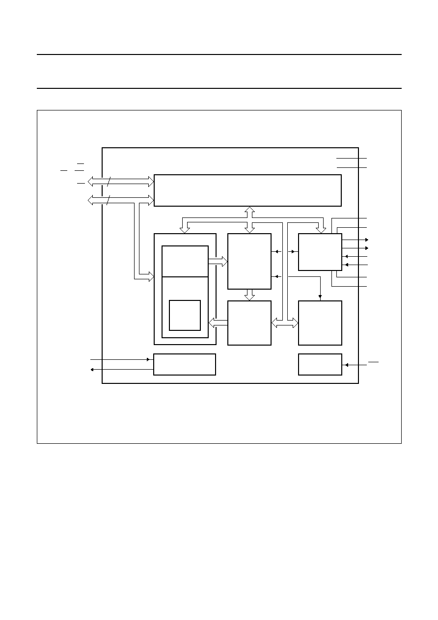
BLOCK DIAGRAM
Fig.1 Block diagram.
handbook, full pagewidth
MGK623
INTERFACE MANAGEMENT LOGIC
7
8 address/data
control
MESSAGE BUFFER
TRANSMIT
BUFFER
RECEIVE
BUFFER
RECEIVE
FIFO
BIT
STREAM
PROCESSOR
ACCEPTANCE
FILTER
BIT TIMING
LOGIC
ERROR
MANAGEMENT
LOGIC
RESET
OSCILLATOR
XTAL1
9
XTAL2
10
TX0
TX1
RX0
RX1
17
18
21
20
19
14
13
15
12
8
22
internal bus
VDD3
VSS3
VDD1
VSS1
VSS2
VDD2
AD7 to AD0
2, 1,
28 to 23
3 to 7,
11, 16
ALE/AS, CS,
RD/E, WR,
CLKOUT,
MODE, INT
RST
SJA1000
2000 Jan 04
5
Philips Semiconductors
Product specification
Stand-alone CAN controller
SJA1000
5
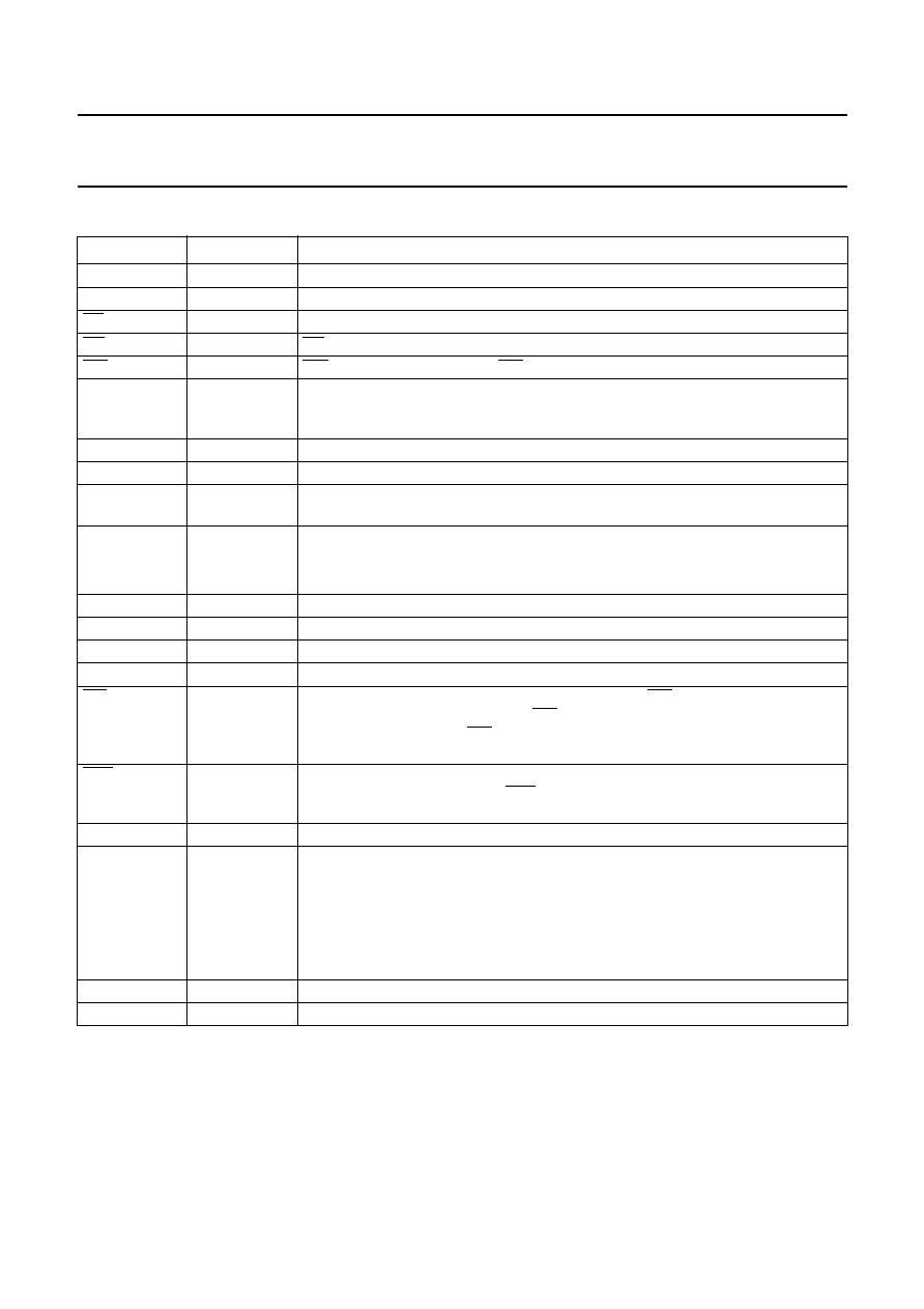
PINNING
Note
1. XTAL1 and XTAL2 pins should be connected to V
SS1
via 15 pF capacitors.
SYMBOL
PIN
DESCRIPTION
AD7 to AD0
2, 1, 28 to 23
multiplexed address/data bus
ALE/AS
3
ALE input signal (Intel mode), AS input signal (Motorola mode)
CS
4
chip select input, LOW level allows access to the SJA1000
RD/E
5
RD signal (Intel mode) or E enable signal (Motorola mode) from the microcontroller
WR
6
WR signal (Intel mode) or RD/WR signal (Motorola mode) from the microcontroller
CLKOUT
7
clock output signal produced by the SJA1000 for the microcontroller; the clock
signal is derived from the built-in oscillator via the programmable divider; the clock
off bit within the clock divider register allows this pin to disable
V
SS1
8
ground for logic circuits
XTAL1
9
input to the oscillator amplifier; external oscillator signal is input via this pin; note 1
XTAL2
10
output from the oscillator amplifier; the output must be left open-circuit when an
external oscillator signal is used; note 1
MODE
11
mode select input
1 = selects Intel mode
0 = selects Motorola mode
V
DD3
12
5 V supply for output driver
TX0
13
output from the CAN output driver 0 to the physical bus line
TX1
14
output from the CAN output driver 1 to the physical bus line
V
SS3
15
ground for output driver
INT
16
interrupt output, used to interrupt the microcontroller; INT is active LOW if any bit of
the internal interrupt register is set; INT is an open-drain output and is designed to
be a wired-OR with other INT outputs within the system; a LOW level on this pin will
reactivate the IC from sleep mode
RST
17
reset input, used to reset the CAN interface (active LOW); automatic power-on reset
can be obtained by connecting RST via a capacitor to V
SS
and a resistor to V
DD
(e.g. C = 1
µ
F; R = 50 k
)
V
DD2
18
5 V supply for input comparator
RX0, RX1
19, 20
input from the physical CAN-bus line to the input comparator of the SJA1000;
a dominant level will wake up the SJA1000 if sleeping; a dominant level is read, if
RX1 is higher than RX0 and vice versa for the recessive level; if the CBP bit (see
Table 49) is set in the clock divider register, the CAN input comparator is bypassed
to achieve lower internal delays if an external transceiver circuitry is connected to
the SJA1000; in this case only RX0 is active; HIGH is interpreted as recessive level
and LOW is interpreted as dominant level
V
SS2
21
ground for input comparator
V
DD1
22
5 V supply for logic circuits