Document Outline
- FEATURES
- DESCRIPTION
- QUICK REFERENCE DATA
- ORDERING INFORMATION
- PIN CONFIGURATION
- PIN DESCRIPTION
- TERMINAL CONFIGURATION
- TERMINAL DESCRIPTION
- BALL CONFIGURATION
- LOGIC DIAGRAM
- FUNCTION TABLE
- ABSOLUTE MAXIMUM RATINGS
- RECOMMENDED OPERATING CONDITIONS
- DC ELECTRICAL CHARACTERISTICS
- TIMING REQUIREMENTS
- SWITCHING CHARACTERISTICS
- OUTPUT BUFFER CHARACTERISTICS
- PARAMETER MEASUREMENT INFORMATION
- AC WAVEFORMS
- Data sheet status
- Definitions
- Disclaimers
Philips
Semiconductors
SSTV16859
2.5 V 13-bit to 26-bit SSTL_2
registered buffer for stacked DDR DIMM
Product data
2000 Dec 01
File under Integrated Circuits -- ICL03
2002 Feb 19
INTEGRATED CIRCUITS
Philips Semiconductors
Product data
SSTV16859
2.5 V 13-bit to 26-bit SSTL_2
registered buffer for stacked DDR DIMM
2
2002 Feb 19
853≠2233 27756
FEATURES
∑
Stub-series terminated logic for 2.5 V V
DD
(SSTL_2)
∑
Optimized for stacked DDR (Double Data Rate) SDRAM
applications
∑
Supports SSTL_2 signal inputs as per JESD 8≠9
∑
Flow-through architecture optimizes PCB layout
∑
ESD classification testing is done to JEDEC Standard JESD22.
Protection exceeds 2000 V to HBM per method A114.
∑
Latch-up testing is done to JEDEC Standard JESD78, which
exceeds 100 mA.
∑
Supports efficient low power standby operation
∑
Full DDR 200/266 solution for stacked DIMMs at 2.5 V when used
with PCKV857
∑
See SSTV16857 for JEDEC compliant register support in
unstacked DIMM applications
∑
See SSTV16856 for driver/buffer version with mode select.
DESCRIPTION
The SSTV16859 is a 13-bit to 26-bit SSTL_2 registered driver with
differential clock inputs, designed to operate between 2.3 V and
2.7 V. All inputs are compatible with the JEDEC standard for
SSTL_2 with V
REF
normally at 0.5*V
DD
, except the LVCMOS reset
(RESET) input. All outputs are SSTL_2, Class II compatible which
can be used for standard stub-series applications or capacitive
loads. Master reset (RESET) asynchronously resets all registers to
zero.
The SSTV16859 is intended to be incorporated into standard DIMM
(Dual In-Line Memory Module) designs defined by JEDEC, such as
DDR (Double Data Rate) SDRAM and SDRAM II Memory Modules.
Different from traditional SDRAM, DDR SDRAM transfers data on
both clock edges (rising and falling), thus doubling the peak bus
bandwidth. A DDR DRAM rated at 133 MHz will have a burst rate of
266 MHz.
The device data inputs consist of different receivers. One differential
input is tied to the input pin while the other is tied to a reference
input pad, which is shared by all inputs.
The clock input is fully differential (CK and CK) to be compatible with
DRAM devices that are installed on the DIMM. Data are registered
at the crossing of CK going high, and CK going low. However, since
the control inputs to the SDRAM change at only half the data rate,
the device must only change state on the positive transition of the
CK signal. In order to be able to provide defined outputs from the
device even before a stable clock has been supplied, the device has
an asynchronous input pin (RESET), which when held to the LOW
state, resets all registers and all outputs to the LOW state.
The device supports low-power standby operation. When RESET is
low, the differential input receivers are disabled, and undriven
(floating) data, clock, and reference voltage (V
REF
) inputs are
allowed. In addition, when RESET is low, all registers are reset, and
all outputs are forced low. The LVCMOS RESET input must always
be held at a valid logic high or low level.
To ensure defined outputs from the register before a stable clock
has been supplied, RESET must be held in the low state during
power-up.
In the DDR DIMM application, RESET is specified to be completely
asynchronous with respect to CK and CK. Therefore, no timing
relationship can be guaranteed between the two. When entering
RESET, the register will be cleared and the outputs will be driven
low. As long as the data inputs are low, and the clock is stable
during the time from the low-to-high transition of RESET until the
input receivers are fully enabled, the outputs will remain low.
Available in 64-pin plastic thin shrink small outline package.
QUICK REFERENCE DATA
GND = 0 V; T
amb
= 25
∞
C; t
r
= t
f
v
2.5 ns
SYMBOL
PARAMETER
CONDITIONS
TYPICAL
UNIT
t
PHL
/t
PLH
Propagation delay; CLK to Qn
C
L
= 30 pF; V
DD
= 2.5 V
2.4
ns
C
I
Input capacitance
V
CC
= 2.5 V
2.7
pF
NOTE:
1. C
PD
is used to determine the dynamic power dissipation (P
D
in
µ
W) P
D
= C
PD
◊
V
CC
2
◊
f
i
+
(C
L
◊
V
CC
2
◊
f
o
) where:
f
i
= input frequency in MHz; C
L
= output load capacity in pF; f
o
= output frequency in MHz; V
CC
= supply voltage in V;
(C
L
◊
V
CC
2
◊
f
o
) = sum of the outputs.
ORDERING INFORMATION
PACKAGES
TEMPERATURE RANGE
ORDER CODE
DWG NUMBER
64-Pin Plastic TSSOP
0 to +70
∞
C
SSTV16859DGG
SOT646AA1
96-Ball Plastic LFBGA
0 to +70
∞
C
SSTV16859EC
SOT536-1
56-Terminal Plastic HVQFN
0 to +70
∞
C
SSTV16859BS
SOT684-1
Philips Semiconductors
Product data
SSTV16859
2.5 V 13-bit to 26-bit SSTL_2
registered buffer for stacked DDR DIMM
2002 Feb 19
3
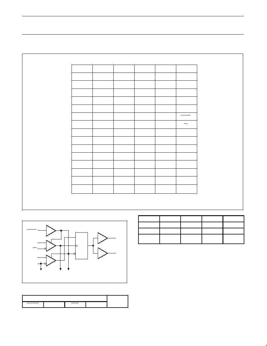
PIN CONFIGURATION
SW00749
1
2
3
4
5
6
7
8
9
10
11
12
53
54
55
56
57
58
59
60
61
62
63
64
Q13A
Q11A
Q10A
Q9A
V
DD
GND
Q8A
Q7A
Q6A
Q5A
V
DD
GND
D13
D12
V
DD
V
DD
GND
D10
D11
D9
GND
D8
Q4A
13
14
15
16
17
18
47
48
49
50
51
52
Q3A
Q2A
GND
Q1A
Q13B
D7
GND
RESET
CK
CK
V
DD
19
46
V
DD
Q12B
20
21
22
23
24
25
40
41
42
43
44
45
Q11B
Q10B
Q9B
Q8B
Q7B
V
DD
GND
V
REF
D5
D4
D3
Q6B
26
39 GND
GND
27
38 V
DD
V
DD
28
29
30
31
32
33
34
35
36
37
Q5B
Q4B
Q3B
Q2B
Q1B
V
DD
D1
GND
V
DD
Q12A
D2
D6
PIN DESCRIPTION
PIN NUMBER
SYMBOL
NAME AND FUNCTION
1, 2, 3, 4, 5, 8,
9, 10, 11, 12,
13, 14, 16
Q13A≠Q1A
Data output
17, 19, 20, 21,
22, 23, 24, 25,
28, 29, 30, 31,
32
Q13B≠Q1B
Data output
6, 18, 27, 33,
37, 38, 46, 47,
59, 60, 64
V
DD
Power supply voltage
7, 15, 26, 34,
39, 43, 50, 54,
58, 63
GND
Ground
35, 36, 40, 41,
42, 44, 52, 53,
55, 56, 57, 61,
62
D1≠D13
Data input: clocked in on the
crossing of the rising edge of CK
and the falling edge of CK
45
V
REF
Input reference voltage
48, 49
CK, CK
Positive and negative master
clock input
51
RESET
Asynchronous reset input:
resets registers and disables
data and clock differential input
receivers
Philips Semiconductors
Product data
SSTV16859
2.5 V 13-bit to 26-bit SSTL_2
registered buffer for stacked DDR DIMM
2002 Feb 19
4
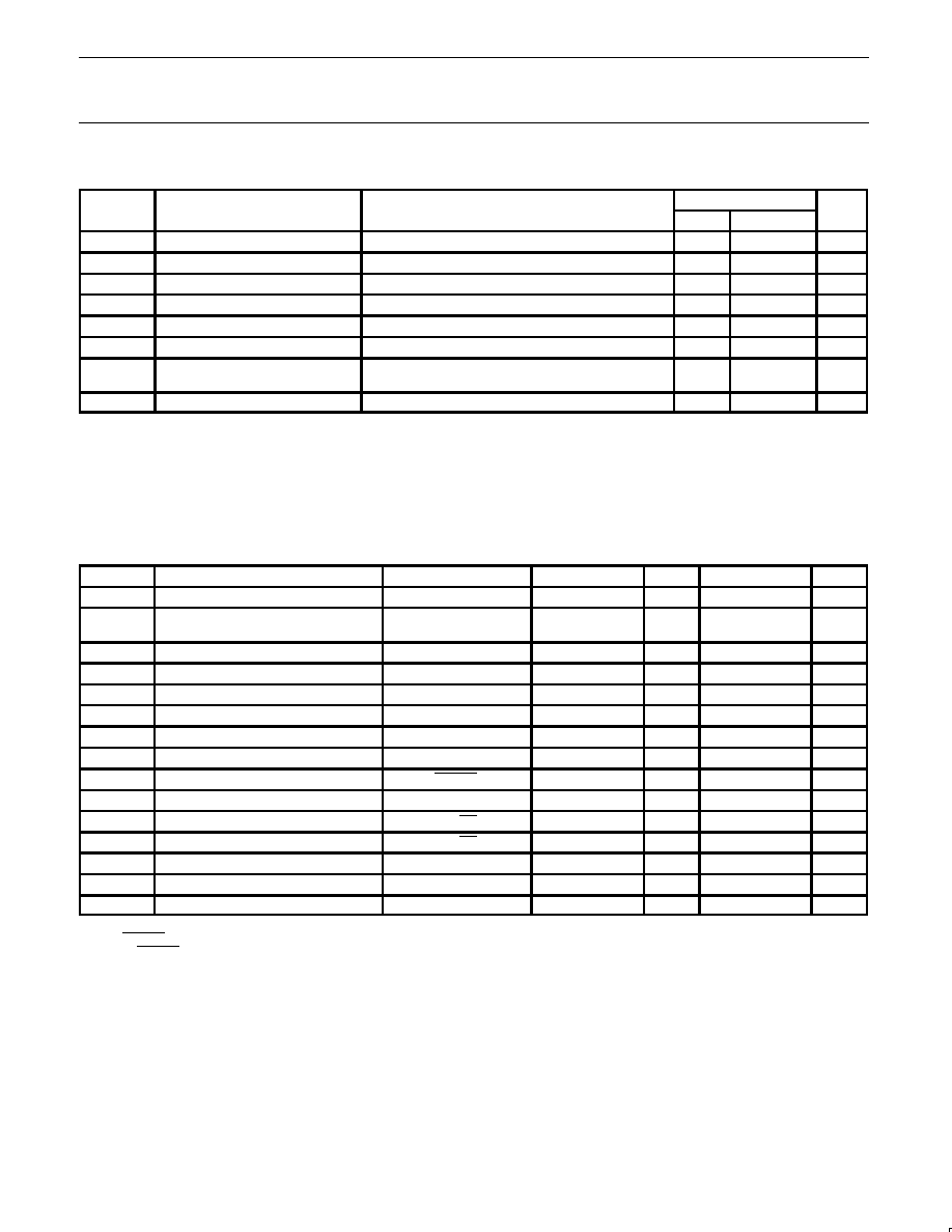
56-TERMINAL CONFIGURATION
14
13
12
11
10
1
2
3
4
5
6
7
8
9
56
55
54
53
52
51
50
49
48
47
46
45
44
43
29
30
31
32
33
42
41
40
39
38
37
36
35
34
15
16
17
18
19
20
21
22
23
24
25
26
27
28
Q7A
Q6A
Q5A
Q4A
Q3A
Q2A
Q1A
Q13B
V
DDQ
Q12B
Q11B
Q10B
Q9B
Q8B
Q7B
Q6B
V
Q5B
Q4B
Q3B
Q2B
Q1B
D1
D2
D3
DDQ
V
DDQ
V
DDI
V
DDQ
D10
D9
D8
D7
GND
CLK
D6
D5
D4
V
REF
V
DDI
V
DDQ
Q8B
Q9A
V
Q10A
Q1
1A
Q12A
Q13A
D13
D12
D1
1
DDQ
GND
V
DDQ
V
DDI
V
DDQ
SW01040
CLK
RESET
TERMINAL DESCRIPTION
TERMINAL
NUMBER
SYMBOL
NAME AND FUNCTION
1, 2, 3, 4, 5, 6,
7, 50, 51, 52,
53, 54, 56
Q13A≠Q1A
Data output
10, 11, 12, 13,
14, 15, 16, 18,
19, 20, 21, 22
Q13B≠Q1B
Data output
9, 17, 23, 27,
34, 44, 49, 55
V
DDQ
Power supply voltage
26, 33, 45
V
DDI
Power supply voltage
37, 48
GND
Ground
24, 25, 28, 29,
30, 31, 39, 40,
41, 42, 43, 46,
47
D1≠D13
Data input: clocked in on the
crossing of the rising edge of CK
and the falling edge of CK
32
V
REF
Input reference voltage
35, 36
CK, CK
Positive and negative master
clock input
51
RESET
Asynchronous reset input:
resets registers and disables
data and clock differential input
receivers
Philips Semiconductors
Product data
SSTV16859
2.5 V 13-bit to 26-bit SSTL_2
registered buffer for stacked DDR DIMM
2002 Feb 19
5
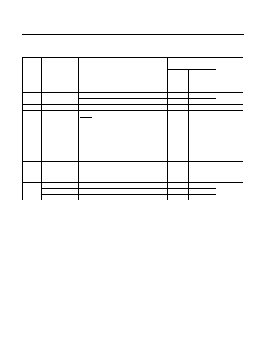
BALL CONFIGURATION
1
2
3
4
5
6
A
B
C
D
E
F
G
H
J
K
L
M
N
P
R
T
Q12A
Q10A
Q8A
Q6A
Q4A
Q2A
Q1A
Q12B
Q10B
Q8B
Q6B
Q4B
Q2B
Q13A
Q11A
Q9A
Q7A
Q5A
Q3A
Q13B
Q11B
Q9B
Q7B
Q5B
Q3B
Q1B
GND
GND
GND
GND
GND
GND
GND
GND
GND
GND
GND
GND
GND
V
DDQ
V
DDQ
V
DDQ
V
DDQ
V
DDQ
V
DDQ
V
DDQ
V
DDQ
V
DDQ
V
DDQ
V
DDQ
V
DDQ
D13
D11
D9
D7
D1
D3
D5
D2
D4
D6
D12
D10
D8
RESET
CK
CK
--
--
--
--
--
--
--
--
--
--
--
--
--
--
--
--
--
--
--
--
--
--
--
--
V
REF
--
--
--
--
SW00944
LOGIC DIAGRAM
SW00750
V
REF
45
D1
35
49
CK
48
CK
51
RESET
1D
C1
R
32
16
to 12 other channels
Q1A
Q1B
FUNCTION TABLE (each flip flop)
INPUTS
OUTPUT
RESET
CLK
CLK
D
Q
H
#
L
L
H
#
H
H
H
L or H
L or H
X
Q
0
L
X or
floating
X or
floating
X or
floating
L
H = High voltage level
L = Low voltage level
= High-to-Low transition
= Low-to-High transition
X = Don't care
Philips Semiconductors
Product data
SSTV16859
2.5 V 13-bit to 26-bit SSTL_2
registered buffer for stacked DDR DIMM
2002 Feb 19
6
ABSOLUTE MAXIMUM RATINGS
1
SYMBOL
PARAMETER
CONDITION
LIMITS
UNIT
SYMBOL
PARAMETER
CONDITION
MIN
MAX
UNIT
V
DD
Supply voltage range
≠0.5
+3.6
V
V
I
Input voltage range
Notes 2 and 3
≠0.5
V
DD
+ 0.5
V
V
O
Output voltage range
Notes 2 and 3
≠0.5
V
DD
+ 0.5
V
I
IK
Input clamp current
V
I
< 0 or V
I
> V
DD
--
±
50
mA
I
OK
Output clamp current
V
O
< 0 or V
O
> V
DD
--
±
50
mA
I
O
Continuous output current
V
O
= 0 to V
DD
--
±
50
mA
Continuous current through each
V
DD
or GND
--
±
100
mA
T
stg
Storage temperature range
≠65
+150
∞
C
NOTES:
1. Stresses beyond those listed under "absolute maximum ratings" may cause permanent damage to the device. These are stress ratings
only and functional operation of the device at these or any other conditions beyond those indicated under "recommended operating
conditions" is not implied. Exposure to absolute-maximum-rated conditions for extended periods may affect device reliability.
2. The input and output negative-voltage ratings may be exceeded if the input and output current ratings are observed.
3. This value is limited to 3.6 V maximum.
4. The performance capability of a high-performance integrated circuit in conjunction with its thermal environment can create junction
temperatures that are detrimental to reliability. The maximum junction temperature of this integrated circuit should not exceed 150
∞
C.
RECOMMENDED OPERATING CONDITIONS
1
SYMBOL
PARAMETER
CONDITIONS
MIN
TYP
MAX
UNIT
V
DD
Supply voltage
V
DD
--
2.7
V
V
REF
Reference voltage
(V
REF
= V
DD
/2)
1.15
1.25
1.35
V
V
TT
Termination voltage
V
REF
≠ 40 mV
V
REF
V
REF
+ 40 mV
V
V
I
Input voltage
0
--
V
DD
V
V
IH
AC HIGH-level input voltage
Data inputs
V
REF
+ 310 mV
--
--
V
V
IL
AC LOW-level input voltage
Data inputs
--
--
V
REF
≠ 310 mV
V
V
IH
DC HIGH-level input voltage
Data inputs
V
REF
+ 150 mV
--
--
V
V
IL
DC LOW-level input voltage
Data inputs
--
--
V
REF
≠ 150 mV
V
V
IH
HIGH-level input voltage
RESET
1.7
--
V
DD
V
V
IL
LOW-level input voltage
0.0
--
0.7
V
V
ICR
Common-mode input range
CK, CK
0.97
--
1.53
V
V
ID
Differential input voltage
CK, CK
360
--
--
mV
I
OH
HIGH-level output current
--
--
≠20
mA
I
OL
LOW-level output current
--
--
20
mA
T
amb
Operating free-air temperature range
0
--
+70
∞
C
NOTE:
1. The RESET input of the device must be held at V
DD
or GND to ensure proper device operation. The differential inputs must not be floating,
unless RESET is low.
Philips Semiconductors
Product data
SSTV16859
2.5 V 13-bit to 26-bit SSTL_2
registered buffer for stacked DDR DIMM
2002 Feb 19
7
DC ELECTRICAL CHARACTERISTICS
Over recommended operating conditions. Voltages are referenced to GND (ground = 0 V).
LIMITS
SYMBOL
PARAMETER
TEST CONDITIONS
T
amb
= 0 to +70
∞
C
UNIT
MIN
TYP
MAX
V
IK
I
I
= ≠18 mA, V
DD
= 2.3 V
--
--
≠1.2
V
V
O
I
OH
= ≠100
µ
A, V
DD
= 2.3 to 2.7 V
V
DD
≠ 0.2
--
--
V
V
OH
I
OH
= ≠16 mA, V
DD
= 2.3 V
1.95
--
--
V
V
O
I
OL
= 100
µ
A, V
DD
= 2.3 to 2.7 V
--
--
0.2
V
V
OL
I
OL
= 16 mA, V
DD
= 2.3 V
--
--
0.35
V
I
I
All inputs
V
I
= V
DD
or GND, V
DD
= 2.7 V
--
--
±
5
µ
A
Static standby
RESET = GND
--
--
0.01
I
DD
Static operating
RESET = V
DD
, V
I
= V
IH(AC)
or
V
IL(AC)
IO = 0, V
DD
= 2.7 V
--
--
45
mA
Dynamic operating ≠
clock only
RESET = V
DD
, V
I
= V
IH(AC)
or
V
IL(AC)
, CK and CK switching
50% duty cycle.
90
--
--
µ
A/ clock MHz
I
DDD
Dynamic operating ≠
per each data input
RESET = V
DD
, V
I
= V
IH(AC)
or
V
IL(AC)
, CK and CK switching
50% duty cycle. One data input
switching at half clock frequency,
50% duty cycle.
IO = 0, V
DD
= 2.7 V
20
--
--
µ
A/ clock MHz/
data input
r
OH
Output high
I
OH
= ≠20 mA, V
DD
= 2.3 to 2.7 V
7
--
20
r
OL
Output low
I
OL
= 20 mA, V
DD
= 2.3 to 2.7 V
7
--
20
r
O(
)
|r
OH
≠ r
OL
|
each separate bit
I
O
= 20 mA, T
amb
= 25
∞
C, V
DD
= 2.5 V
--
--
4
Data inputs
V
I
= V
REF
±
310 mV, V
DD
= 2.5 V
2.5
2.74
3.5
C
i
CK and CK
V
ICR
= 1.25 V, V
I(PP)
= 360 mV, V
DD
= 2.5 V
2.5
3.15
3.5
pF
RESET
V
I
= V
DD
or GND, V
DD
= 2.5 V
--
2.27
--
Philips Semiconductors
Product data
SSTV16859
2.5 V 13-bit to 26-bit SSTL_2
registered buffer for stacked DDR DIMM
2002 Feb 19
8
TIMING REQUIREMENTS
Over recommended operating conditions; T
amb
= 0 to +70
∞
C (unless otherwise noted) (see Figure 1)
LIMITS
SYMBOL
PARAMETER
TEST CONDITIONS
V
DD
= 2.5 V
±
0.2 V
UNIT
MIN
MAX
f
clock
Clock frequency
--
200
MHz
t
w
Pulse duration, CK, CK HIGH or LOW
2.5
--
ns
t
act
Differential inputs active time
Notes 1, 2
--
22
ns
t
inact
Differential inputs inactive time
Notes 1, 3
--
22
ns
t
Setup time, fast slew rate
(see Notes 4 and 6)
Data before CK
CK
0.75
ns
t
su
Setup time, slow slew rate
(see Notes 5 and 6)
Data before CK
, CK
0.9
ns
t
Hold time, fast slew rate
(see Notes 4 and 6)
Data after CK
CK
0.75
ns
t
h
Hold time, slow slew rate
(see Notes 5 and 6)
Data after CK
, CK
0.9
ns
t
SL
Output slew
1
6
V/ns
NOTES:
1. This parameter is not necessarily production tested.
2. Data inputs must be below a minimum time of t
act
max, after RESET is taken high.
3. Data and clock inputs must be held at valid levels (not floating) a minimum time of t
inact
max, after RESET is taken low.
4. For data signal input slew rate
1 V/ns.
5. For data signal input slew rate
0.5 V/ns and < 1 V/ns.
6. CK, CK signals input slew rates are
1 V/ns.
SWITCHING CHARACTERISTICS
Over recommended operating conditions; T
amb
= 0 to +70
∞
C; V
DD
= 2.3 ≠ 2.7 V
.
Class I, V
REF
= V
TT
= V
DD
◊
0.5 and C
L
= 10 pF (unless otherwise noted) (see Figure 1)
O
O
LIMITS
SYMBOL
FROM
(INPUT)
TO
(OUTPUT)
V
DD
= 2.5 V
±
0.2 V
UNIT
(INPUT)
(OUTPUT)
MIN
MAX
f
max
200
--
MHz
t
pd
CK and CK
Q
1.1
2.8
ns
t
PHL
RESET
Q
1.1
5
ns
Philips Semiconductors
Product data
SSTV16859
2.5 V 13-bit to 26-bit SSTL_2
registered buffer for stacked DDR DIMM
2002 Feb 19
9
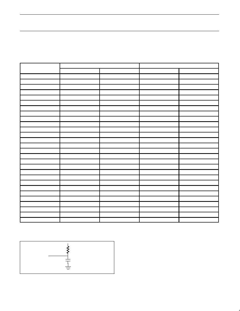
OUTPUT BUFFER CHARACTERISTICS
The following table describes output-buffer Voltage vs. Current (V/I) characteristics that are sufficient to meet the requirements of registered
DDR DIMM performance and timings. These characteristics are not necessarily production tested but can be guaranteed by design or
characterization. Compliance with these curves is not mandatory if it can be adequately demonstrated that alternate characteristics meet the
requirements of the registered DDR DIMM application.
VOLTAGE (V)
PULL-DOWN
PULL-UP
I (mA) MIN
I (mA) MAX
I (mA) MIN
I (mA) MAX
0.0
0
0
0
0
0.1
7
11
7
10
0.2
14
23
14
20
0.3
21
34
21
30
0.4
28
44
27
40
0.5
33
54
33
49
0.6
39
64
38
59
0.7
44
74
44
68
0.8
48
83
49
76
0.9
52
91
53
84
1.0
56
99
57
93
1.1
59
107
61
100
1.2
61
114
64
108
1.3
63
121
67
115
1.4
64
127
69
121
1.5
66
133
70
128
1.6
66
138
72
134
1.7
67
142
73
139
1.8
67
146
74
144
1.9
67
149
74
148
2.0
67
151
75
152
2.1
68
153
75
156
2.2
68
154
75
159
2.3
68
155
76
161
2.4
--
156
--
163
2.5
--
157
--
165
2.6
--
157
--
167
2.7
--
157
--
168
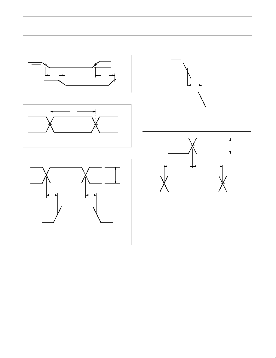
PARAMETER MEASUREMENT INFORMATION
TEST CIRCUIT
Test Point
From Output
C
L
= 30 pF
see Note 1
R
L
= 50
SW00751
Under Test
Figure 1. Load circuitry
NOTE:
1. C
L
includes probe and jig capacitance.
Philips Semiconductors
Product data
SSTV16859
2.5 V 13-bit to 26-bit SSTL_2
registered buffer for stacked DDR DIMM
2002 Feb 19
10
AC WAVEFORMS
SW00752
V
DD
/2
LVCMOS
RESET
10%
I
DD
t
inact
V
DD
V
DD
/2
t
act
90%
Waveform 1. Inputs active and inactive times (see Note 1)
V
REF
V
REF
V
IH
V
IL
INPUT
SW00753
t
W
Waveform 2. Pulse duration
SW00754
V
ICR
V
ICR
V
I(PP)
TIMING
INPUT
OUTPUT
t
PLH
t
PHL
V
TT
V
OH
V
OL
Waveform 3. Propagation delay times
Input
SW00755
V
IH
LVCMOS RESET
V
DD
/2
V
IL
V
OH
V
OL
V
TT
t
PHL
Output
Waveform 4. Propagation delay times
V
ICR
V
I(PP)
Timing input
SW00756
V
REF
V
REF
V
IL
Input
t
h
t
su
V
IH
Waveform 5. Setup and hold times
NOTES:
1. I
DD
tested with clock and data inputs held at V
DD
or GND, and I
O
= 0 mA.
2. All input pulses are supplied by generators having the following characteristics: PRR
10 MHz, Z
O
= 50
, input slew rate = 1 V/ns
±
20%
(unless otherwise specified).
3. The outputs are measured one at a time with one transition per measurement.
4. V
TT
= V
REF
= V
DD
/2
5. V
IH
= V
REF
+ 310 mV (ac voltage levels) for differential inputs. V
IH
= V
DD
for LVCMOS input.
6. V
IL
= V
REF
≠ 310 mV (ac voltage levels) for differential inputs. V
IL
= GND for LVCMOS input.
7. t
PLH
and t
PHL
are the same as t
pd
.
Philips Semiconductors
Product data
SSTV16859
2.5 V 13-bit to 26-bit SSTL_2
registered buffer for stacked DDR DIMM
2002 Feb 19
11
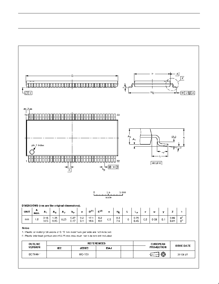
TSSOP64:
plastic thin shrink small outline package; 64 leads; body width 6.1 mm
SOT646-1
Philips Semiconductors
Product data
SSTV16859
2.5 V 13-bit to 26-bit SSTL_2
registered buffer for stacked DDR DIMM
2002 Feb 19
12
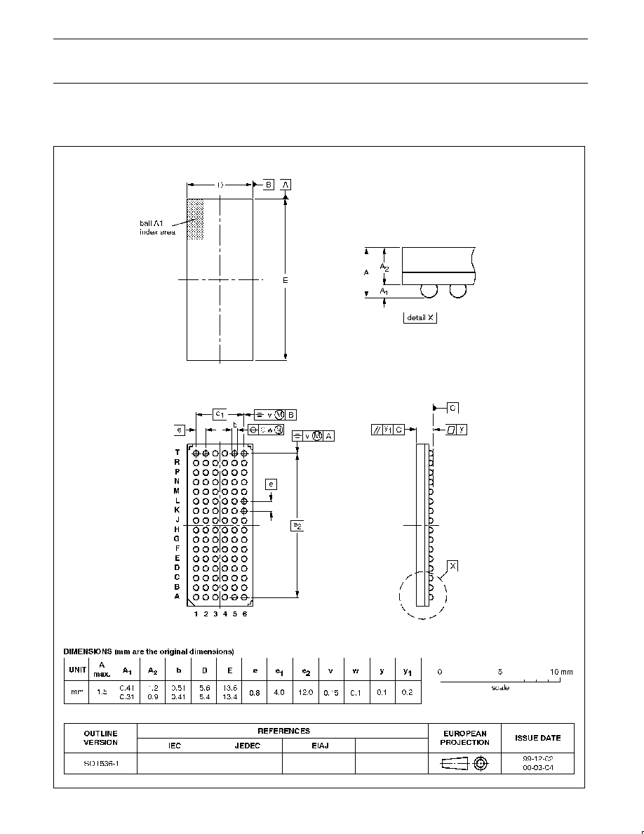
LFBGA96:
plastic low profile fine-pitch ball grid array package; 96 balls;
body 13.5 x 5.5 x 1.05 mm
SOT536-1
Philips Semiconductors
Product data
SSTV16859
2.5 V 13-bit to 26-bit SSTL_2
registered buffer for stacked DDR DIMM
2002 Feb 19
13
HVQFN56:
plastic, heatsink very thin quad flat package; no leads; 56 terminals;
body 8 x 8 x 0.85 mm
SOT684-1
Philips Semiconductors
Product data
SSTV16859
2.5 V 13-bit to 26-bit SSTL_2
registered buffer for stacked DDR DIMM
2002 Feb 19
14
Definitions
Short-form specification -- The data in a short-form specification is extracted from a full data sheet with the same type number and title. For
detailed information see the relevant data sheet or data handbook.
Limiting values definition -- Limiting values given are in accordance with the Absolute Maximum Rating System (IEC 60134). Stress above one
or more of the limiting values may cause permanent damage to the device. These are stress ratings only and operation of the device at these or
at any other conditions above those given in the Characteristics sections of the specification is not implied. Exposure to limiting values for extended
periods may affect device reliability.
Application information -- Applications that are described herein for any of these products are for illustrative purposes only. Philips
Semiconductors make no representation or warranty that such applications will be suitable for the specified use without further testing or
modification.
Disclaimers
Life support -- These products are not designed for use in life support appliances, devices or systems where malfunction of these products can
reasonably be expected to result in personal injury. Philips Semiconductors customers using or selling these products for use in such applications
do so at their own risk and agree to fully indemnify Philips Semiconductors for any damages resulting from such application.
Right to make changes -- Philips Semiconductors reserves the right to make changes, without notice, in the products, including circuits, standard
cells, and/or software, described or contained herein in order to improve design and/or performance. Philips Semiconductors assumes no
responsibility or liability for the use of any of these products, conveys no license or title under any patent, copyright, or mask work right to these
products, and makes no representations or warranties that these products are free from patent, copyright, or mask work right infringement, unless
otherwise specified.
Contact information
For additional information please visit
http://www.semiconductors.philips.com.
Fax: +31 40 27 24825
For sales offices addresses send e-mail to:
sales.addresses@www.semiconductors.philips.com.
©
Koninklijke Philips Electronics N.V. 2002
All rights reserved. Printed in U.S.A.
Date of release: 02-02
Document order number:
9397 750 09464
Philips
Semiconductors
Data sheet status
[1]
Objective data
Preliminary data
Product data
Product
status
[2]
Development
Qualification
Production
Definitions
This data sheet contains data from the objective specification for product development.
Philips Semiconductors reserves the right to change the specification in any manner without notice.
This data sheet contains data from the preliminary specification. Supplementary data will be
published at a later date. Philips Semiconductors reserves the right to change the specification
without notice, in order to improve the design and supply the best possible product.
This data sheet contains data from the product specification. Philips Semiconductors reserves the
right to make changes at any time in order to improve the design, manufacturing and supply.
Changes will be communicated according to the Customer Product/Process Change Notification
(CPCN) procedure SNW-SQ-650A.
Data sheet status
[1] Please consult the most recently issued data sheet before initiating or completing a design.
[2] The product status of the device(s) described in this data sheet may have changed since this data sheet was published. The latest information is available on the Internet at URL
http://www.semiconductors.philips.com.