
1997 Jul 15
2
Philips Semiconductors
Preliminary specification
Photodetector amplifiers and laser
supplies
TDA1300T; TDA1300TT
FEATURES
∑
Six input buffer amplifiers with low-pass filtering with
virtually no offset
∑
HF data amplifier with a high or low gain mode
∑
Two built-in equalizers for single or double speed mode
ensuring high playability in both modes
∑
Full automatic laser control including stabilization and
an on/off switch and containing a separate supply V
DDL
for power reduction
∑
Applicable with N-sub laser with N-sub or P-sub monitor
diode
∑
Adjustable laser bandwidth and laser switch-on current
slope
∑
Protection circuit preventing laser damage due to supply
voltage dip
∑
Optimized interconnect between pick-up detector and
TDA1301
∑
Wide supply voltage range
∑
Wide temperature range
∑
Low power consumption.
GENERAL DESCRIPTION
The TDA1300 is an integrated data amplifier and laser
supply for three beam pick-up detectors applied in a wide
range of mechanisms for Compact Disc (CD) and read
only optical systems. It offers 6 amplifiers which amplify
and filter the focus and radial diode signals adequately and
provides an equalized RF signal for single or double speed
mode which can be switched by means of the speed
control pin.
The device can handle astigmatic, single Foucault and
double Foucault detectors and is applicable with all N-sub
lasers and N-sub or P-sub monitor diode units.
After a single initial adjustment the circuit keeps control
over the laser diode current resulting in a constant light
output power independent of ageing. The chip is mounted
in a small SO24 or TSSOP24 package enabling mounting
close to the laser pick-up unit on the sledge.
QUICK REFERENCE DATA
ORDERING INFORMATION
SYMBOL
PARAMETER
CONDITIONS
MIN.
TYP.
MAX.
UNIT
V
DD
supply voltage
3
-
5.5
V
Diode current amplifiers (n = 1 to 6)
G
d(n)
diode current gain
1.43
1.55
1.67
I
O(d)
diode offset current
-
-
100
nA
B
3 dB bandwidth
I
i(d)
= 1.67
µ
A
50
-
-
kHz
RFE amplifier (built-in equalizer)
t
d(eq)
equalization delay
f
i
= 0.3 MHz
-
320
-
ns
t
d(f)
flatness delay
double speed
-
5
-
ns
Laser supply
I
o(L)
output current
V
DDL
= 3 V
-
-
-
100
mA
TYPE
NUMBER
PACKAGE
NAME
DESCRIPTION
VERSION
TDA1300T
SO24
plastic small outline package; 24 leads; body width 7.5 mm
SOT137-1
TDA1300TT
TSSOP24
plastic thin shrink small outline package; 24 leads; body width 4.4 mm
SOT355-1
1997 Jul 15
4
Philips Semiconductors
Preliminary specification
Photodetector amplifiers and laser
supplies
TDA1300T; TDA1300TT
PINNING
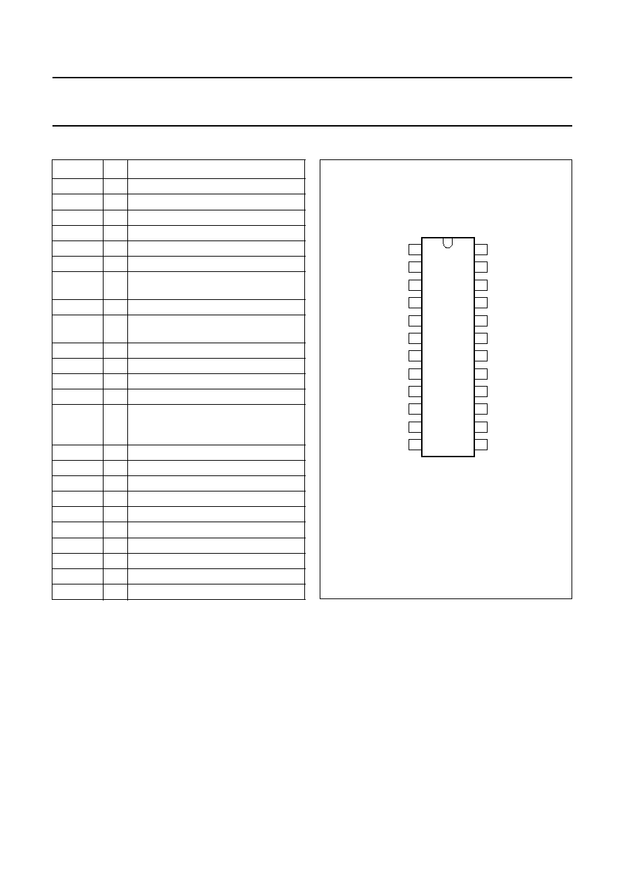
SYMBOL PIN
DESCRIPTION
O4
1
current amplifier 4 output
O6
2
current amplifier 6 output
O3
3
current amplifier 3 output
O1
4
current amplifier 1 output
O5
5
current amplifier 5 output
O2
6
current amplifier 2 output
LDON
7
control pin for switching the laser on
and off
V
DDL
8
laser supply voltage
RFE
9
equalized output voltage of sum signal
of amplifiers 1 to 4
RF
10
unequalized output
HG
11
control pin for gain switch
LS
12
control pin for speed switch
CL
13
external capacitor
ADJ
14
P-sub monitor (if connected via
resistor to GND);
N-sub monitor (if connected to V
DD
)
GND
15
ground (substrate connection)
LO
16
laser output; current output
MI
17
monitor diode input (laser)
V
DD
18
supply
I2
19
photo detector input 2 (central)
I5
20
photo detector input 5 (satellite)
I1
21
photo detector input 1 (central)
I3
22
photo detector input 3 (central)
I6
23
photo detector input 6 (satellite)
I4
24
photo detector input 4 (central)
Fig.2 Pin configuration.
handbook, halfpage
TDA1300T
1
2
3
4
5
6
7
8
9
10
11
12
O4
O6
O3
O1
O5
O2
LDON
VDDL
RFE
RF
HG
LS
I4
I6
I3
I1
I5
I2
VDD
MI
LO
GND
ADJ
CL
24
23
22
21
20
19
18
17
16
15
14
13
MBG472

1997 Jul 15
5
Philips Semiconductors
Preliminary specification
Photodetector amplifiers and laser
supplies
TDA1300T; TDA1300TT
FUNCTIONAL DESCRIPTION
The TDA1300T; TDA1300TT can be divided into two main
sections:
∑
Laser control circuit section
∑
Photo diode signal filter and amplification section.
Laser control circuit section
The main function of the laser control circuit is to control
the laser diode current in order to achieve a constant light
output power. This is done by monitoring the monitor
diode. There is a fixed relation between light output power
of the laser and the current of the monitor diode. The circuit
can handle P-sub or N-sub monitor diodes.
N-sub
MONITOR
In this event pin 14 (ADJ) must be connected to the
positive supply voltage V
DD
to select the N-sub mode. With
an adjustable resistor (R
ADJn
) across the diode the monitor
current can be adjusted (and so the laser light output
power) if one knows that the control circuit keeps the
monitor voltage V
mon
at a constant level of
approximately 150 mV.
P-sub
MONITOR
In this event pin 14 (ADJ) is connected via resistor R
ADJp
to ground. The P-sub mode is selected and pin 14 (ADJ)
acts as reference band gap voltage, providing together
with R
ADJp
an adjustable current l
ADJ
. Now the control
circuit keeps the monitor current at a level which is 10l
ADJ
.
The circuit is built up in three parts:
∑
The first part is the input stage which is able to switch
between both modes (N-sub or P-sub).
∑
The second part is the integrator part which makes use
of an external capacitor C
L
. This capacitor has two
different functions:
≠ During switch-on of the laser current, it provides a
current slope of typically:
(A/s)
≠ After switch-on it ensures that the bandwidth equals
(Hz)
in case of P-sub monitor or
I
o(L)
t
--------------
10
6
≠
C
L
-----------
B
P
K
G
ext
◊
90
9
≠
◊
10
◊
C
L
I
mon
◊
--------------------------------------------------
(Hz)
in case of N-sub monitor, where
G
ext
represents the AC gain of an extra loop amplifier,
if applied, and K =
I
mon
/
I
L
which is determined by
the laser/monitor unit. I
mon
is the average current
(pin 17) at typical light emission power of the laser
diode.
∑
The third part is the power output stage, its input being
the integrator output signal. This stage has a separate
supply voltage (V
DDL
), thereby offering the possibility of
reduced power consumption by supplying this pin with
the minimum voltage necessary.
It also has a laser diode protection circuit which comes into
action just before the driving output transistor will get
saturated due to a large voltage dip on V
DDL
. Saturation
will result in a lower current of the laser diode, which
normally is followed immediately by an increment of the
voltage of the external capacitor C
L
. This could cause
damage to the laser diode at the end of the dip.
The protection circuit prevents an increment of the
capacitor voltage and thus offers full protection to the laser
diode under these circumstances.
Photo diode signal filter and amplification section
This section has 6 identical current amplifiers.
Amplifiers 1 to 4 are designed to amplify the focus photo
diode signals. Each amplifier has two outputs: an
LF output and an internal RF output. Amplifiers 5 and 6
are used for the radial photo diode currents and only have
an LF output. All 6 output signals are low-pass filtered with
a corner frequency at 69 kHz. The internal RF output
signals are summed together and converted to a voltage
afterwards by means of a selectable transresistance.
This transresistance R
RF
can be changed between 140 k
(3.3 V application) or 240 k
(5 V application) in
combination with the P-sub monitor. In the event of the
N-sub monitor selection, R
RF
can be changed between
70 k
(3.3 V application) and 120 k
(5 V application).
The RF signal is available directly at pin 10 but there is
also an unfiltered signal available at pin 9.
The used equalization filter has 2 different filter curves:
∑
One for single-speed mode
∑
One for double-speed mode.
B
N
R
ADJn
C
L
---------------- K
G
ext
◊
870
9
≠
◊
10
◊

