Document Outline
- FEATURES
- APPLICATION
- GENERAL DESCRIPTION
- ORDERING INFORMATION
- QUICK REFERENCE DATA
- BLOCK DIAGRAM
- PINNING
- FUNCTIONAL DESCRIPTION
- LIMITING VALUES
- THERMAL CHARACTERISTICS
- QUALITY SPECIFICATION
- CHARACTERISTICS
- PACKAGE OUTLINE
- SOLDERING
- DEFINITIONS
- LIFE SUPPORT APPLICATIONS

DATA SHEET
Product specification
Supersedes data of 1996 Jun 04
File under Integrated Circuits, IC01
1996 Oct 21
INTEGRATED CIRCUITS
TDA1309H
Low-voltage low-power stereo
bitstream ADC/DAC

1996 Oct 21
2
Philips Semiconductors
Product specification
Low-voltage low-power stereo bitstream
ADC/DAC
TDA1309H
FEATURES
∑
Low power
∑
Low supply voltage (2.7 V)
∑
Integrated high-pass filter to cancel DC offset (ADC)
∑
Analog loop-through function
∑
Multiple digital input/output formats possible
∑
256f
s
system clock frequency
∑
Several power-down modes
∑
Digital de-emphasis (DAC)
∑
Overload detector to enable automatic recording level
adjustment (ADC)
∑
Input pads suitable for 5.5 V; low supply voltage
interfacing
∑
High dynamic range
∑
DAC requires only one capacitor for post-filtering
∑
Small 44-pin quad flat pack with 0.8 mm pitch
∑
256f
s
system clock frequency in Analog-to-Digital (AD)
and Digital-to-Analog (DA) mode
∑
Choice of three system clock frequencies
(192f
s
, 256f
s
or 384f
s
) in DA mode.
APPLICATION
∑
Portable digital audio equipment.
GENERAL DESCRIPTION
The TDA1309H is a single chip stereo analog-to-digital
and digital-to-analog converter employing bitstream
conversion techniques. The low voltage requirement
makes the device eminently suitable for use in low-voltage
low-power portable digital audio equipment which
incorporates recording and playback functions.
ORDERING INFORMATION
TYPE NUMBER
PACKAGE
NAME
DESCRIPTION
VERSION
TDA1309H
QFP44
plastic quad flat package; 44 leads (lead length 1.3 mm);
body 10
◊
10
◊
1.75 mm
SOT307-2

1996 Oct 21
3
Philips Semiconductors
Product specification
Low-voltage low-power stereo bitstream
ADC/DAC
TDA1309H
QUICK REFERENCE DATA
V
DDD
= V
DDA
= V
DDO
= V
DDD(F)
= 3 V; V
SSD
= V
SSA
= V
SSO
= V
SSD(F)
= 0 V; T
amb
= 25
∞
C; full scale sine wave input;
mode 1; f
i
= 1 kHz; 16-bit input data; conversion rate = 44.1 kHz; measurement bandwidth = 10 Hz to 20 kHz; unless
otherwise specified.
Notes
1. The input voltage for full scale digital output is a function of V
DDA(AD)
.
2. At full scale digital input; no de-emphasis; V
O(rms)
is a function of V
DDA(DA)
.
3. 18-bit input data.
SYMBOL
PARAMETER
CONDITIONS
MIN.
TYP.
MAX. UNIT
Supply
V
DDA(AD)
ADC analog supply voltage (pin 8)
2.7
3.0
4.0
V
V
DDA(DA)
DAC analog supply voltage (pin 25)
2.7
3.0
4.0
V
V
DDO
operational amplifiers supply voltage
(pin 19)
2.7
3.0
4.0
V
V
DDD
ADC and DAC digital supply voltage
(pin 28)
2.7
3.0
4.0
V
V
DDD(F)
digital filters supply voltage (pin 34)
2.7
3.0
4.0
V
I
DDA(AD)
ADC analog supply current (pin 8)
-
8
12.5
mA
I
DDA(DA)
DAC analog supply current (pin 25)
-
3.5
7
mA
I
DDO
operational amplifiers supply current
(pin 19)
-
12
18
mA
I
DDD
ADC and DAC digital supply current
(pin 28)
-
0.2
0.5
mA
I
DDD(F)
digital filters supply current (pin 34)
-
20
30
mA
I
PD(DA)
DAC power-down current
-
15
20
mA
I
PD(AD)
ADC power-down current
-
7
10
mA
T
amb
operating ambient temperature
-
20
-
+75
∞
C
Analog-to-digital converter
V
I(rms)
input voltage (RMS value)
note 1
-
0.5
0.54
V
(THD + N)/S total harmonic distortion plus
noise-to-signal ratio
at 0 dB
-
-
85
-
80
dB
at
-
60 dB; A-weighted
-
-
35
-
30
dB
S/N
idle channel signal-to-noise ratio
V
I
= 0 V; A-weighted
90
95
-
dB
cs
channel separation
-
90
-
dB
Digital-to-analog converter
V
O(rms)
output voltage (RMS value)
note 2
0.43
0.5
0.57
V
(THD + N)/S total harmonic distortion plus
noise-to-signal ratio
at 0 dB
-
-
90
-
82
dB
at
-
60 dB; A-weighted
-
-
38
-
34
dB
at
-
60 dB; A-weighted; note 3
-
-
44
-
dB
S/N
idle channel signal-to-noise ratio
code 0000H; A-weighted
-
104
-
dB
cs
channel separation
90
100
-
dB

1996 Oct 21
4
Philips Semiconductors
Product specification
Low-voltage low-power stereo bitstream
ADC/DAC
TDA1309H
BLOCK DIAGRAM
book, full pagewidth
MGE766
4.7 k
4.7 k
4.7 k
4.7 k
1.5 k
1.5 k
1.5 k
1.5 k
750
750
47
µ
F
0.22
µ
F
0.22
µ
F
47
µ
F
0.22
µ
F
2.2 nF
2.2 nF
330 pF
330 pF
27
k
10
µ
F
0.22
µ
F
Vm
Vm
DAC
DIGITAL
FILTER
DIGITAL
FILTER
DAC
DIGITAL
INTERFACE
DIGITAL
INTERFACE
MODE SELECT
ADC
ADC
CURRENT
REFERENCE
14
15
42
1
41
6
36
32
31
35
29
5
39
28
27
23
24
18
22
21
19
20
26
25
33
34
30
3
42
43
44
37
38
40
9
11
12
13
10
16
7
8
17
AD
ref
BAIR
BA
OR
O
VLO
AD
ADENB
AD
WS
ADBCK
ADSD
A
ADPON
ANLPTR
DA
W
S
D
ABCK
D
ASD
A
D
APON
V
SS(I/O)
V
DDD
V
SSD
DA
C
R
V
OR
analog output
V
OR
DA
ref
analog input
V
IR
V
OL
DACL
analog output
V
OL
V
SSO
V
DDO
V
SSA(DA)
V
DDA(DA)
V
SSD(F)
V
DDD(F)
DADEM
MODE0
MODE1
MODE2
CLKEDGE
TEST0
TEST1
SYSCLK
V
ref(neg)
V
ref(pos)
BAOL
BAIL
V
ref
V
DDA(AD)
analog input
V
IL
V
SSA(AD)
V
DDA(AD)
I ref
I DAC
TDA1309H
Supply decoupling on pins 19, 25, 28 and 34; 0.22
µ
F (ceramic), 47
µ
F (electrolytic).
Capacitance at pin 11 should be close to pins 11 and 9.
Fig.1 Block diagram.

1996 Oct 21
5
Philips Semiconductors
Product specification
Low-voltage low-power stereo bitstream
ADC/DAC
TDA1309H
PINNING
SYMBOL
PIN
DESCRIPTION
ADBCK
1
ADC input bit clock; 32f
s
or 64f
s
ADWS
2
ADC word select input at f
s
MODE0
3
ADC/DAC mode select input
ADENB
4
ADC serial data enable input (active HIGH)
OVLOAD
5
ADC output overload flag (active LOW)
ADPON
6
ADC power-on-mode input (active HIGH)
V
SSA(AD)
7
ADC analog ground supply voltage
V
DDA(AD)
8
ADC analog supply voltage
V
ref(neg)
9
ADC negative reference voltage input (ground)
V
ref
10
ADC decoupling capacitor
V
ref(pos)
11
ADC positive reference voltage decoupling capacitor
BAOL
12
ADC input amplifier output left
BAIL
13
ADC input amplifier virtual ground left
BAIR
14
ADC input amplifier virtual ground right
BAOR
15
ADC input amplifier output right
AD
ref
16
ADC decoupling capacitor
I
ref
17
ADC/DAC reference current resistor input
DA
ref
18
DAC decoupling capacitor
V
DDO
19
ADC/DAC operational amplifier supply voltage
V
SSO
20
ADC/DAC operational amplifier ground supply voltage
V
OL
21
DAC output voltage left
DACL
22
DAC output current left
DACR
23
DAC output current right
V
OR
24
DAC output voltage right
V
DDA(DA)
25
DAC analog supply voltage
V
SSA(DA)
26
DAC analog ground supply voltage
V
SSD
27
ADC/DAC digital ground supply voltage
V
DDD
28
ADC/DAC digital supply voltage
DAPON
29
DAC power-on-mode input (active HIGH)
DADEM
30
DAC digital de-emphasis input (active HIGH)
DABCK
31
DAC input bit clock; 32f
s
, 48f
s
or 64f
s
DAWS
32
DAC word select input at f
s
V
SSD(F)
33
ADC/DAC digital filters ground supply voltage
V
DDD(F)
34
ADC/DAC digital filters supply voltage
DASDA
35
DAC serial data input
ANLPTR
36
ADC/DAC analog loop-through input (active HIGH)
TEST0
37
ADC/DAC enable test mode 0 input (LOW is normal mode)
TEST1
38
ADC/DAC enable test mode 1 input (LOW is normal mode)
V
SS(I/O)
39
ADC/DAC digital input/output ground supply voltage
SYSCLK
40
ADC/DAC system clock input (f
sys
= 256f
s
; DAC also 192f
s
and 384f
s
)

1996 Oct 21
6
Philips Semiconductors
Product specification
Low-voltage low-power stereo bitstream
ADC/DAC
TDA1309H
ADSDA
41
ADC serial data output
MODE1
42
ADC/DAC mode 1 select input
MODE2
43
ADC/DAC mode 2 select input
CLKEDGE
44
ADC/DAC input bit clock rising/falling edge
SYMBOL
PIN
DESCRIPTION
Fig.2 Pin configuration.
handbook, full pagewidth
1
2
3
4
5
6
7
8
9
10
11
33
32
31
30
29
28
27
26
25
24
23
12
13
14
15
16
17
18
19
20
21
22
44
43
42
41
40
39
38
37
36
35
34
TDA1309H
MGE765
VSSD(F)
DAWS
DABCK
DADEM
VDDD
VSSD
VSSA(DA)
VDDA(DA)
VOR
DACR
ADBCK
ADWS
MODE0
ADENB
OVLOAD
ADPON
VDDA(AD)
Vref(neg)
Vref(pos)
DAPON
MODE2
MODE1
ADSDA
SYSCLK
V
SS(I/O)
TEST1
ANLPTR
DASDA
V
DDD(F)
CLKEDGE
TEST0
BAIL
BAIR
BAOR
AD
ref
I ref
DA
ref
V
SSO
V
OL
DACL
BAOL
V
DDO
VSSA(AD)
Vref

1996 Oct 21
7
Philips Semiconductors
Product specification
Low-voltage low-power stereo bitstream
ADC/DAC
TDA1309H
FUNCTIONAL DESCRIPTION
Figure 1 illustrates the various components of the
TDA1309H.
The analog-to-digital converter is a bitstream type
converter, both channels are sampled simultaneously.
The digital-to-analog converter is a BCC (Bitstream
Continuous Calibration) type converter. The digital filter for
the ADC is a bit serial IIR filter that produces a fairly linear
phase response up to 15 kHz. A high-pass filter is
incorporated in the down-sampling path to remove DC
offsets. An overload detection circuit is incorporated to
facilitate automatic recording level adjustment.
The digital up-sample filter for the DAC is partly IIR, with
virtual linear phase response up to 15 kHz, and partly FIR.
A switchable digital de-emphasis circuit is also
incorporated. Due to the BCC principle used, the DAC
needs only single pole post-filtering (one external
capacitor) to meet the out-of-band suppression
requirement.
The ADC and DAC channels have separate power-down
modes, to reduce power if one of them is not in use.
An analog loop-through function enables analog-input
analog-output mode without using the ADC and DAC
converters or filters, thereby switching them off to reduce
power consumption.
The digital interfaces accommodates, 16 and 18-bit,
I
2
S-bus and LSB justified formats. The ADC digital output
can be made 3-state by means of the ADENB signal, this
enables the use of a digital bus.
The TDA1309H interface accommodates slave mode only,
therefore, the system ICs must provide the system clock,
bit clock and word clock signals. For the DAC, the
TDA1309H accepts the data together with these clocks,
for the ADC it delivers the data in response to these clocks.
Within one stereo frame, the first sample always
represents the left channel. When sending data the
unused bit positions are set to zero, when receiving data
these bit positions are don't cares.
To accommodate the various interface formats and
system clock frequencies four control pins are provided,
MODE0 to MODE2 for mode selection and CLKEDGE
which selects the active edge of the BCK signal. Table 1
gives the interface mode selection, Fig.3 illustrates the
ADC/DAC data formats and Fig.5 the operating modes.
The section of the TDA1309H is designed to
accommodate two main modes:
1. The 256f
s
mode in which analog-to-digital and
digital-to-analog can be used
2. The 192f
s
or 384f
s
mode (digital-to-analog only).
Table 1
Interface mode selection
Note
1. Only digital-to-analog.
Table 2
Clock edge mode
DEVICE PIN
ADC/DAC FORMATS
MODE 2
MODE 1
MODE 0
TYPE
BITS
BCK
SYS; f
sys
FIGURE
0
0
0
LSB justified
16
32f
s
256f
s
3(a)
0
0
1
LSB justified
16
64f
s
256f
s
3(b)
0
1
0
LSB justified
16
48f
s
192f
s
(1)
4(a)
0
1
1
LSB justified
18
64f
s
256f
s
3(c)
1
0
0
I
2
S-bus
16
32f
s
256f
s
3(d)
1
0
1
I
2
S-bus
16
64f
s
256f
s
3(e)
1
1
0
I
2
S-bus
16
48f
s
384f
s
(1)
4(b)
1
1
1
I
2
S-bus
18
64f
s
256f
s
3(f)
CLKEDGE
VALID EDGE OF BCK
ADC
DAC
0
falling
rising
1
rising
falling

1996 Oct 21
8
Philips Semiconductors
Product specification
Low-voltage low-power stereo bitstream
ADC/DAC
TDA1309H
Fig.3 DAC and ADC data formats (continued in Fig.4).
handbook, full pagewidth
MGE767
BCK
WS
SDA
BCK
WS
SDA
BCK
WS
SDA
BCK
WS
SDA
BCK
WS
SDA
BCK
WS
SDA
LSB MSB
LEFT
LSB MSB
RIGHT
LEFT
RIGHT
LEFT
RIGHT
LEFT
RIGHT
LEFT
RIGHT
LEFT
RIGHT
LSB MSB
LSB MSB
LSB
MSB
LSB MSB
LSB
MSB
LSB
LSB
MSB
LSB
MSB
LSB
MSB
MSB
LSB
MSB
LSB
MSB
LSB
MSB
LSB
MSB
LSB
I
2
S 64fs 18-BIT
I
2
S 64fs 16-BIT
I
2
S 32fs 16-BIT
LSB JUSTIFIED 64fs 18-BIT
LSB JUSTIFIED 64fs 16-BIT
LSB JUSTIFIED 32fs 16-BIT
(a)
(b)
(c)
(d)
(e)
(f)
1996 Oct 21
9
Philips Semiconductors
Product specification
Low-voltage low-power stereo bitstream
ADC/DAC
TDA1309H
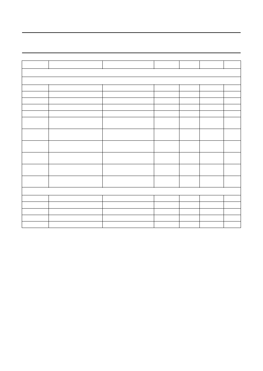
There are different modes in which the TDA1309H can operate. These modes can be selected as shown in Table 3 and
Fig.5. In mode a, the digital filters clock is switched off. Switching over to one of the ADC active modes (b, c or d) initiates
a reset sequence of the digital filters. This mode should be activated immediately after power-on for at least 2 clock
periods.
Table 3
Operating mode selection
Note
1. X = don't care.
MODE
DESCRIPTION
DEVICE PIN LOGIC
ANLPTR
ADPON
DAPON
a
not used
0
0
0
b
record and playback
0
1
1
c
record only
0
1
0
d
record and analog loop-through
1
1
0
e
analog loop-through
1
0
0
f
playback only
0
0
1
g and h
reserved
1
X
(1)
1
Fig.4 DAC and ADC data formats (continued from Fig.3).
handbook, full pagewidth
BCK
WS
SDA
BCK
WS
SDA
LSB
MSB
LSB
MSB
LSB
MSB
LSB
MSB
LSB
MSB
LEFT
LEFT
RIGHT
RIGHT
LSB JUSTIFIED 48fs 16-BIT
I
2
S 48fs 16-BIT
(a)
(b)
MGE768

1996 Oct 21
10
Philips Semiconductors
Product specification
Low-voltage low-power stereo bitstream
ADC/DAC
TDA1309H
Fig.5 Schematic diagram of operating modes.
handbook, full pagewidth
MGE771
MODE b
analog
input
ADC
ANALOG
ADC
DIGITAL
FILTER
ADC
ANALOG
ADC
DIGITAL
FILTER
ADC
ANALOG
ADC
DIGITAL
FILTER
analog
output
digital
input
DAC
ANALOG
DAC
DIGITAL
FILTER
DAC
ANALOG
DAC
DIGITAL
FILTER
MODE c
analog
input
digital
output
digital
output
MODE d
analog
input
analog
output
MODE e
analog
input
analog
output
MODE f
analog
output
digital
input
digital
output

1996 Oct 21
11
Philips Semiconductors
Product specification
Low-voltage low-power stereo bitstream
ADC/DAC
TDA1309H
LIMITING VALUES
In accordance with the Absolute Maximum Rating System (IEC 134).
Notes
1. Human body model: C = 100 pF; R = 1.5 k
; 3 zaps positive and 3 zaps negative.
2. Machine model: C = 200 pF; L = 0.5
µ
H; R = 10
; 3 zaps positive and 3 zaps negative.
THERMAL CHARACTERISTICS
QUALITY SPECIFICATION
In accordance with
"SNW-FQ-611E". The number of this quality specification can be found in the "Quality Reference
Handbook". The handbook can be ordered using the code 9397 750 00192.
SYMBOL
PARAMETER
CONDITIONS
MIN.
MAX.
UNIT
V
DDA(AD)
analog supply voltage (pin 8)
-
4.5
V
V
DDA(DA)
analog supply voltage (pin 25)
-
4.5
V
V
DDO
operational amplifiers supply voltage
(pin 19)
-
4.5
V
V
DDD
digital supply voltage (pin 28)
-
4.5
V
V
DDD(F)
digital filters supply voltage (pin 34)
-
4.5
V
V
DD
maximum supply voltage difference
-
100
mV
V
SS
maximum ground supply voltage
difference
-
100
mV
V
I
maximum input voltage
-
0.5
V
DD
+ 0.5
V
I
IK
DC clamp input diode current
V
I
<
-
0.5 V or
V
I
> V
DD
+ 0.5 V
-
±
10
mA
I
OK
DC output clamp diode current;
(output type 2 mA)
V
O
<
-
0.5 V or
V
O
> V
DD
+ 0.5 V
-
±
10
mA
T
stg
storage temperature
-
65
+150
∞
C
T
amb
operating ambient temperature
-
20
+75
∞
C
V
es
electrostatic handling
note 1
-
1500
+1500
V
note 2
-
300
+300
V
SYMBOL
PARAMETER
VALUE
UNIT
R
th j-a
thermal resistance from junction to ambient in free air
60
K/W

1996 Oct 21
12
Philips Semiconductors
Product specification
Low-voltage low-power stereo bitstream
ADC/DAC
TDA1309H
CHARACTERISTICS
V
DDD
= V
DDA
= V
DDO
= V
DDD(F)
= 3 V; V
SSD
= V
SSA
= V
SSO
= V
SSD(F)
= 0 V; T
amb
= 25
∞
C; full scale sine wave input;
mode 1; f
i
= 1 kHz; 16-bit input data; conversion rate = 44.1 kHz; measurement bandwidth = 10 Hz to 20 kHz; unless
otherwise specified.
SYMBOL
PARAMETER
CONDITIONS
MIN.
TYP.
MAX.
UNIT
Supply
V
DDA(AD)
ADC analog supply
voltage (pin 8)
2.7
3.0
4.0
V
V
DDA(DA)
DAC analog supply
voltage (pin 25)
2.7
3.0
4.0
V
V
DDO
operational amplifiers
supply voltage (pin 19)
2.7
3.0
4.0
V
V
DDD
ADC/DAC digital supply
voltage (pin 28)
2.7
3.0
4.0
V
V
DDD(F)
digital filters supply voltage
(pin 34)
2.7
3.0
4.0
V
I
DDA(AD)
ADC analog supply current
(pin 8)
-
8
12.5
mA
ADC power-down
-
0.3
1
mA
I
DDA(DA)
DAC analog supply current
(pin 25)
-
3.5
7
mA
DAC power-down
-
1.4
2
mA
I
DDO
operational amplifiers
supply current (pin 19)
-
12
18
mA
DAC power-down
-
5.5
9
mA
ADC power-down
-
7
11
mA
ADC/DAC power-down
-
0
-
mA
I
DDD
ADC/DAC digital supply
current (pin 28)
-
0.2
0.5
mA
I
DDD(F)
digital filters supply current
(pin 34)
-
20
30
mA
DAC power-down
-
15
20
mA
ADC power-down
-
7
10
mA
I
DDD(F)q
digital filters quiescent
current
-
-
100
µ
A

1996 Oct 21
13
Philips Semiconductors
Product specification
Low-voltage low-power stereo bitstream
ADC/DAC
TDA1309H
Analog-to-digital converter
V
I(rms)
input voltage (RMS value)
note 1
-
0.5
0.54
V
I
I
input current
(pins 13 and 14)
-
-
10
nA
V
O
unbalance between
channels
-
-
0.3
dB
RES
resolution
16-bit format
-
16
-
bits
18-bit format
-
18
-
bits
(THD + N)/S total harmonic distortion
plus noise-to-signal ratio
at 0 dB
-
-
85
-
80
dB
at
-
20 dB
-
-
75
-
dB
at
-
60 dB; A-weighted
-
-
35
-
30
dB
S/N
idle channel
signal-to-noise ratio
V
i
= 0 V; A-weighted
90
95
-
dB
cs
channel separation
-
90
-
dB
PSRR
power supply rejection ratio note 2
-
-
30
-
dB
Digital-to-analog converter
V
O(rms)
output voltage
(RMS value)
note 3
0.43
0.5
0.57
V
V
O
unbalance between
channels
-
0.1
-
dB
R
L
load resistance
5
-
-
k
C
L
load capacitance
note 4
-
-
200
pF
RES
resolution
16-bit format
-
16
-
bits
18-bit format
-
18
-
bits
(THD + N)/S total harmonic distortion
plus noise-to-signal ratio
at 0 dB
-
-
90
-
82
dB
at
-
20 dB
-
-
75
-
dB
at
-
60 dB; A-weighted
-
-
38
-
34
dB
at
-
60 dB; A-weighted;
note 5
-
-
44
-
dB
S/N
idle channel
signal-to-noise ratio
code 0000H; A-weighted
-
104
-
dB
cs
channel separation
90
100
-
dB
PSRR
power supply rejection ratio note 2
-
-
30
-
dB
Analog loop-through (mode e)
(THD + N)/S total harmonic distortion
plus noise-to-signal ratio
at 0 dB
-
-
85
-
dB
S/N
idle channel
signal-to-noise ratio
V
I
= 0 V; A-weighted
-
95
-
dB
G
ltr
loop-through gain
note 1
-
-
1.1
-
dB
E
os
DC offset error
-
1.0
-
mV
SYMBOL
PARAMETER
CONDITIONS
MIN.
TYP.
MAX.
UNIT

1996 Oct 21
14
Philips Semiconductors
Product specification
Low-voltage low-power stereo bitstream
ADC/DAC
TDA1309H
Analog-to-digital decimation filter
f
s(o)
output sample frequency
28
44.1
54
kHz
f
s(i)
input sample frequency
-
128f
s
-
f
sys
system clock frequency
256f
s
-
256f
s
B
signal bandwidth
f
s(o)
= 44.1 kHz
0.02
-
20
kHz
A
sup
aliasing suppression
f
s(o)
-
B < f
i
< 2f
s(o)
-
B;
note 6
60
-
-
dB
f
i
> 2f
s(o)
-
B; note 6
80
-
-
dB
frequency response
f
i
= 20 Hz to 20 kHz
-
0.2
-
+0.2
dB
OL
det
overload detection level
note 7
-
0.11
-
dB
Digital-to-analog interpolation filter
f
s(o)
output sample frequency
-
64f
s
-
f
s(i)
input sample frequency
28
44.1
54
kHz
f
sys
system clock frequency
256f
s
-
256f
s
B
signal bandwidth
f
s(i)
= 44.1 kHz
0.02
-
20
kHz
frequency response
f
i
= 20 Hz to 20 kHz
-
0.2
-
+0.2
dB
SUP
out-of-band suppression
40
50
-
dB
Digital part; note 8
I
NPUTS
(
PINS
1
TO
4, 6, 29
TO
32, 35
TO
38, 40
AND
42
TO
44)
V
IL
LOW level input voltage
-
0.5
-
0.3V
DDD
V
I
IL
LOW level input current
V
I
= V
SSD
-
-
10
µ
A
I
IH
HIGH level input current
V
I
= V
DDD
-
-
10
µ
A
C
I(max)
maximum input
capacitance
-
-
10
pF
I
NPUTS
(
PINS
1
TO
4, 6, 29
TO
32, 35
TO
38, 40
AND
42)
V
IH
HIGH level input voltage
0.7V
DDD
-
5.5
V
I
NPUTS
(
PINS
43
AND
44)
V
IH
HIGH level input voltage
0.7V
DDD
-
V
DDD
+ 0.5
V
O
UTPUTS
(
PINS
5
AND
41)
V
OL
LOW level output voltage
I
OL
= 2 mA
-
-
0.5
V
V
OH
HIGH level output voltage
I
OH
=
-
2 mA
V
DDD
-
0.5
-
-
V
I
OZ
3-state leakage current
V
O
= V
DDD
or V
SSD
-
-
10
µ
A
SYMBOL
PARAMETER
CONDITIONS
MIN.
TYP.
MAX.
UNIT
1996 Oct 21
15
Philips Semiconductors
Product specification
Low-voltage low-power stereo bitstream
ADC/DAC
TDA1309H
Notes
1. V
I
for full scale digital output is a function of V
DDA(AD)
, 0.5 V (RMS) (at 3 V the digital voltages are equivalent to
-
1.1 dB in the digital domain).
2. V
ripple
= 1% of the supply voltage and f
ripple
= 100 Hz.
3. At full scale digital input; no de-emphasis; V
O(rms)
is a function of V
DDA(DA)
.
4. For a load capacitance greater than 33 pF a series resistor of 200
is recommended.
5. 18 bits input data.
6. The aliasing suppression frequency is mirrored around 128f
s
.
7. V
DDA
= 3 V; indicated digital level is with respect to
-
1.1 dB (no overload).
8. All digital voltages = 2.7 to 4.0 V; all ground supply voltages = 0 V; T
amb
=
-
20 to +75
∞
C.
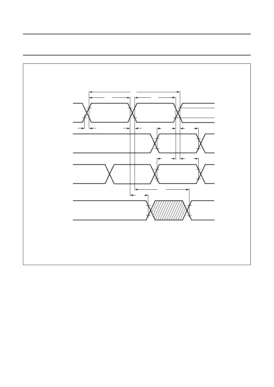
Timing
B
IT CLOCK
(BCK)
RELATED SIGNALS
(see Fig.6); CLKEDGE = 0
T
cy
clock period
300
-
-
ns
t
HC
clock HIGH time
100
-
-
ns
t
LC
clock LOW time
100
-
-
ns
t
r
rise time
-
-
20
ns
t
f
fall time
-
-
20
ns
t
suWS
set-up time WS to rising
edge of BCK
20
-
-
ns
t
hWS
hold time WS to rising edge
of BCK
0
-
-
ns
t
suDA
set-up time SDA (DAC) to
rising edge of BCK
20
-
-
ns
t
hDA
hold time SDA (DAC) to
rising edge of BCK
0
-
-
ns
t
hAD
hold time SDA (ADC) to
falling edge of BCK
0
-
-
ns
t
dAD
delay time SDA (ADC) to
falling edge of BCK
-
-
80
ns
S
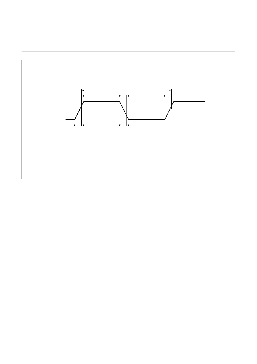
YSTEM CLOCK
(SYSCLK)
RELATED SIGNALS
(see Fig.7)
T
cy
clock period
72
-
-
ns
t
HC
clock HIGH time
22
-
-
ns
t
LC
clock LOW time
22
-
-
ns
t
r
rise time
-
-
10
ns
t
f
fall time
-
-
10
ns
SYMBOL
PARAMETER
CONDITIONS
MIN.
TYP.
MAX.
UNIT
1996 Oct 21
16
Philips Semiconductors
Product specification
Low-voltage low-power stereo bitstream
ADC/DAC
TDA1309H
Fig.6 Serial timing of BCK related signals.
handbook, full pagewidth
MGE769
tHC
tLC
Tcy
tr
tf
tsuWS
thWS
tsuDA
thDA
tdAD
thAD
VH
VL
CLKEDGE = 1
CLKEDGE = 0
BCK
WS (LRCK)
SDA (DAC)
SDA (ADC)
1996 Oct 21
17
Philips Semiconductors
Product specification
Low-voltage low-power stereo bitstream
ADC/DAC
TDA1309H
Fig.7 Serial timing of SYSCLK related signals.
handbook, full pagewidth
MGE770
tHC
tLC
Tcy
tr
tf
SYSCLK

1996 Oct 21
18
Philips Semiconductors
Product specification
Low-voltage low-power stereo bitstream
ADC/DAC
TDA1309H
PACKAGE OUTLINE
UNIT
A
1
A
2
A
3
b
p
c
E
(1)
e
H
E
L
L
p
Q
Z
y
w
v
REFERENCES
OUTLINE
VERSION
EUROPEAN
PROJECTION
ISSUE DATE
IEC
JEDEC
EIAJ
mm
0.25
0.05
1.85
1.65
0.25
0.40
0.20
0.25
0.14
10.1
9.9
0.8
1.3
12.9
12.3
0.85
0.75
1.2
0.8
10
0
o
o
0.15
0.1
0.15
DIMENSIONS (mm are the original dimensions)
Note
1. Plastic or metal protrusions of 0.25 mm maximum per side are not included.
0.95
0.55
SOT307-2
92-11-17
95-02-04
D
(1)
(1)
(1)
10.1
9.9
H
D
12.9
12.3
E
Z
1.2
0.8
D
e
E
B
11
c
E
H
D
ZD
A
Z E
e
v
M
A
X
1
44
34
33
23
22
12
y
A
1
A
L
p
Q
detail X
L
(A )
3
A
2
pin 1 index
D
H
v
M
B
b
p
b
p
w
M
w
M
0
2.5
5 mm
scale
QFP44: plastic quad flat package; 44 leads (lead length 1.3 mm); body 10 x 10 x 1.75 mm
SOT307-2
A
max.
2.10

1996 Oct 21
19
Philips Semiconductors
Product specification
Low-voltage low-power stereo bitstream
ADC/DAC
TDA1309H
SOLDERING
Introduction
There is no soldering method that is ideal for all IC
packages. Wave soldering is often preferred when
through-hole and surface mounted components are mixed
on one printed-circuit board. However, wave soldering is
not always suitable for surface mounted ICs, or for
printed-circuits with high population densities. In these
situations reflow soldering is often used.
This text gives a very brief insight to a complex technology.
A more in-depth account of soldering ICs can be found in
our
"IC Package Databook" (order code 9398 652 90011).
Reflow soldering
Reflow soldering techniques are suitable for all QFP
packages.
The choice of heating method may be influenced by larger
plastic QFP packages (44 leads, or more). If infrared or
vapour phase heating is used and the large packages are
not absolutely dry (less than 0.1% moisture content by
weight), vaporization of the small amount of moisture in
them can cause cracking of the plastic body. For more
information, refer to the Drypack chapter in our
"Quality
Reference Handbook" (order code 9398 510 63011).
Reflow soldering requires solder paste (a suspension of
fine solder particles, flux and binding agent) to be applied
to the printed-circuit board by screen printing, stencilling or
pressure-syringe dispensing before package placement.
Several techniques exist for reflowing; for example,
thermal conduction by heated belt. Dwell times vary
between 50 and 300 seconds depending on heating
method. Typical reflow temperatures range from
215 to 250
∞
C.
Preheating is necessary to dry the paste and evaporate
the binding agent. Preheating duration: 45 minutes at
45
∞
C.
Wave soldering
Wave soldering is not recommended for QFP packages.
This is because of the likelihood of solder bridging due to
closely-spaced leads and the possibility of incomplete
solder penetration in multi-lead devices.
If wave soldering cannot be avoided, the following
conditions must be observed:
∑
A double-wave (a turbulent wave with high upward
pressure followed by a smooth laminar wave)
soldering technique should be used.
∑
The footprint must be at an angle of 45
∞
to the
board direction and must incorporate solder
thieves downstream and at the side corners.
Even with these conditions, do not consider wave
soldering the following packages:
QFP52 (SOT379-1), QFP100 (SOT317-1),
QFP100 (SOT317-2), QFP100 (SOT382-1) or
QFP160 (SOT322-1).
During placement and before soldering, the package
must be fixed with a droplet of adhesive. The adhesive
can be applied by screen printing, pin transfer or syringe
dispensing. The package can be soldered after the
adhesive is cured.
Maximum permissible solder temperature is 260
∞
C, and
maximum duration of package immersion in solder is
10 seconds, if cooled to less than 150
∞
C within
6 seconds. Typical dwell time is 4 seconds at 250
∞
C.
A mildly-activated flux will eliminate the need for removal
of corrosive residues in most applications.
Repairing soldered joints
Fix the component by first soldering two diagonally-
opposite end leads. Use only a low voltage soldering iron
(less than 24 V) applied to the flat part of the lead.
Contact time must be limited to 10 seconds at up to
300
∞
C. When using a dedicated tool, all other leads can
be soldered in one operation within 2 to 5 seconds
between 270 and 320
∞
C.

1996 Oct 21
20
Philips Semiconductors
Product specification
Low-voltage low-power stereo bitstream
ADC/DAC
TDA1309H
DEFINITIONS
LIFE SUPPORT APPLICATIONS
These products are not designed for use in life support appliances, devices, or systems where malfunction of these
products can reasonably be expected to result in personal injury. Philips customers using or selling these products for
use in such applications do so at their own risk and agree to fully indemnify Philips for any damages resulting from such
improper use or sale.2
Data sheet status
Objective specification
This data sheet contains target or goal specifications for product development.
Preliminary specification
This data sheet contains preliminary data; supplementary data may be published later.
Product specification
This data sheet contains final product specifications.
Limiting values
Limiting values given are in accordance with the Absolute Maximum Rating System (IEC 134). Stress above one or
more of the limiting values may cause permanent damage to the device. These are stress ratings only and operation
of the device at these or at any other conditions above those given in the Characteristics sections of the specification
is not implied. Exposure to limiting values for extended periods may affect device reliability.
Application information
Where application information is given, it is advisory and does not form part of the specification.

1996 Oct 21
21
Philips Semiconductors
Product specification
Low-voltage low-power stereo bitstream
ADC/DAC
TDA1309H
NOTES

1996 Oct 21
22
Philips Semiconductors
Product specification
Low-voltage low-power stereo bitstream
ADC/DAC
TDA1309H
NOTES

1996 Oct 21
23
Philips Semiconductors
Product specification
Low-voltage low-power stereo bitstream
ADC/DAC
TDA1309H
NOTES

Internet: http://www.semiconductors.philips.com
Philips Semiconductors ≠ a worldwide company
© Philips Electronics N.V. 1996
SCA52
All rights are reserved. Reproduction in whole or in part is prohibited without the prior written consent of the copyright owner.
The information presented in this document does not form part of any quotation or contract, is believed to be accurate and reliable and may be changed
without notice. No liability will be accepted by the publisher for any consequence of its use. Publication thereof does not convey nor imply any license
under patent- or other industrial or intellectual property rights.
Netherlands: Postbus 90050, 5600 PB EINDHOVEN, Bldg. VB,
Tel. +31 40 27 82785, Fax. +31 40 27 88399
New Zealand: 2 Wagener Place, C.P.O. Box 1041, AUCKLAND,
Tel. +64 9 849 4160, Fax. +64 9 849 7811
Norway: Box 1, Manglerud 0612, OSLO,
Tel. +47 22 74 8000, Fax. +47 22 74 8341
Philippines: Philips Semiconductors Philippines Inc.,
106 Valero St. Salcedo Village, P.O. Box 2108 MCC, MAKATI,
Metro MANILA, Tel. +63 2 816 6380, Fax. +63 2 817 3474
Poland: Ul. Lukiska 10, PL 04-123 WARSZAWA,
Tel. +48 22 612 2831, Fax. +48 22 612 2327
Portugal: see Spain
Romania: see Italy
Russia: Philips Russia, Ul. Usatcheva 35A, 119048 MOSCOW,
Tel. +7 095 247 9145, Fax. +7 095 247 9144
Singapore: Lorong 1, Toa Payoh, SINGAPORE 1231,
Tel. +65 350 2538, Fax. +65 251 6500
Slovakia: see Austria
Slovenia: see Italy
South Africa: S.A. PHILIPS Pty Ltd., 195-215 Main Road Martindale,
2092 JOHANNESBURG, P.O. Box 7430 Johannesburg 2000,
Tel. +27 11 470 5911, Fax. +27 11 470 5494
South America: Rua do Rocio 220, 5th floor, Suite 51,
04552-903 S„o Paulo, S√O PAULO - SP, Brazil,
Tel. +55 11 821 2333, Fax. +55 11 829 1849
Spain: Balmes 22, 08007 BARCELONA,
Tel. +34 3 301 6312, Fax. +34 3 301 4107
Sweden: Kottbygatan 7, Akalla, S-16485 STOCKHOLM,
Tel. +46 8 632 2000, Fax. +46 8 632 2745
Switzerland: Allmendstrasse 140, CH-8027 ZÐRICH,
Tel. +41 1 488 2686, Fax. +41 1 481 7730
Taiwan: PHILIPS TAIWAN Ltd., 23-30F, 66,
Chung Hsiao West Road, Sec. 1, P.O. Box 22978,
TAIPEI 100, Tel. +886 2 382 4443, Fax. +886 2 382 4444
Thailand: PHILIPS ELECTRONICS (THAILAND) Ltd.,
209/2 Sanpavuth-Bangna Road Prakanong, BANGKOK 10260,
Tel. +66 2 745 4090, Fax. +66 2 398 0793
Turkey: Talatpasa Cad. No. 5, 80640 GÐLTEPE/ISTANBUL,
Tel. +90 212 279 2770, Fax. +90 212 282 6707
Ukraine: PHILIPS UKRAINE, 4 Patrice Lumumba str., Building B, Floor 7,
252042 KIEV, Tel. +380 44 264 2776, Fax. +380 44 268 0461
United Kingdom: Philips Semiconductors Ltd., 276 Bath Road, Hayes,
MIDDLESEX UB3 5BX, Tel. +44 181 730 5000, Fax. +44 181 754 8421
United States: 811 East Arques Avenue, SUNNYVALE, CA 94088-3409,
Tel. +1 800 234 7381
Uruguay: see South America
Vietnam: see Singapore
Yugoslavia: PHILIPS, Trg N. Pasica 5/v, 11000 BEOGRAD,
Tel. +381 11 625 344, Fax.+381 11 635 777
For all other countries apply to: Philips Semiconductors, Marketing & Sales Communications,
Building BE-p, P.O. Box 218, 5600 MD EINDHOVEN, The Netherlands, Fax. +31 40 27 24825
Argentina: see South America
Australia: 34 Waterloo Road, NORTH RYDE, NSW 2113,
Tel. +61 2 9805 4455, Fax. +61 2 9805 4466
Austria: Computerstr. 6, A-1101 WIEN, P.O. Box 213,
Tel. +43 1 60 101, Fax. +43 1 60 101 1210
Belarus: Hotel Minsk Business Center, Bld. 3, r. 1211, Volodarski Str. 6,
220050 MINSK, Tel. +375 172 200 733, Fax. +375 172 200 773
Belgium: see The Netherlands
Brazil: see South America
Bulgaria: Philips Bulgaria Ltd., Energoproject, 15th floor,
51 James Bourchier Blvd., 1407 SOFIA,
Tel. +359 2 689 211, Fax. +359 2 689 102
Canada: PHILIPS SEMICONDUCTORS/COMPONENTS,
Tel. +1 800 234 7381
China/Hong Kong: 501 Hong Kong Industrial Technology Centre,
72 Tat Chee Avenue, Kowloon Tong, HONG KONG,
Tel. +852 2319 7888, Fax. +852 2319 7700
Colombia: see South America
Czech Republic: see Austria
Denmark: Prags Boulevard 80, PB 1919, DK-2300 COPENHAGEN S,
Tel. +45 32 88 2636, Fax. +45 31 57 1949
Finland: Sinikalliontie 3, FIN-02630 ESPOO,
Tel. +358 9 615800, Fax. +358 9 61580/xxx
France: 4 Rue du Port-aux-Vins, BP317, 92156 SURESNES Cedex,
Tel. +33 1 40 99 6161, Fax. +33 1 40 99 6427
Germany: Hammerbrookstraþe 69, D-20097 HAMBURG,
Tel. +49 40 23 53 60, Fax. +49 40 23 536 300
Greece: No. 15, 25th March Street, GR 17778 TAVROS/ATHENS,
Tel. +30 1 4894 339/239, Fax. +30 1 4814 240
Hungary: see Austria
India: Philips INDIA Ltd, Shivsagar Estate, A Block, Dr. Annie Besant Rd.
Worli, MUMBAI 400 018, Tel. +91 22 4938 541, Fax. +91 22 4938 722
Indonesia: see Singapore
Ireland: Newstead, Clonskeagh, DUBLIN 14,
Tel. +353 1 7640 000, Fax. +353 1 7640 200
Israel: RAPAC Electronics, 7 Kehilat Saloniki St, TEL AVIV 61180,
Tel. +972 3 645 0444, Fax. +972 3 649 1007
Italy: PHILIPS SEMICONDUCTORS, Piazza IV Novembre 3,
20124 MILANO, Tel. +39 2 6752 2531, Fax. +39 2 6752 2557
Japan: Philips Bldg 13-37, Kohnan 2-chome, Minato-ku, TOKYO 108,
Tel. +81 3 3740 5130, Fax. +81 3 3740 5077
Korea: Philips House, 260-199 Itaewon-dong, Yongsan-ku, SEOUL,
Tel. +82 2 709 1412, Fax. +82 2 709 1415
Malaysia: No. 76 Jalan Universiti, 46200 PETALING JAYA, SELANGOR,
Tel. +60 3 750 5214, Fax. +60 3 757 4880
Mexico: 5900 Gateway East, Suite 200, EL PASO, TEXAS 79905,
Tel. +9-5 800 234 7381
Middle East: see Italy
Printed in The Netherlands
517021/1200/04/pp24
Date of release: 1996 Oct 21
Document order number:
9397 750 00879