Document Outline
- FEATURES
- GENERAL DESCRIPTION
- ORDERING INFORMATION
- QUICK REFERENCE DATA
- BLOCK DIAGRAM
- PINNING
- FUNCTIONAL DESCRIPTION
- LIMITING VALUES
- THERMAL RESISTANCE
- QUALITY SPECIFICATION
- CHARACTERISTICS
- APPLICATION INFORMATION
- Basic application example
- Attention to printed circuit board layout
- Interface examples
- Evaluation of audio parameters
- PACKAGE OUTLINES
- SOLDERING
- DEFINITIONS
- LIFE SUPPORT APPLICATIONS

DATA SHEET
Preliminary specification
Supersedes data of July 1993
File under Integrated Circuits, IC01
1995 Dec 18
INTEGRATED CIRCUITS
TDA1311A
Stereo Continuous Calibration DAC
(CC-DAC)
1995 Dec 18
2
Philips Semiconductors
Preliminary specification
Stereo Continuous Calibration DAC
(CC-DAC)
TDA1311A
FEATURES
∑
Voltage output
∑
Space saving packages SO8 or DIP8
∑
Low power consumption
∑
Wide dynamic range (16-bit resolution)
∑
Continuous Calibration (CC) concept
∑
Easy application:
≠ single 4 to 5.5 V rail supply
≠ output current and bias current are proportional to the
supply voltage
≠ integrated current-to-voltage converter
∑
Fast settling time permits 2, 4 and 8
◊
oversampling
(serial input) or double-speed operation at
4
◊
oversampling
∑
Internal bias current ensures maximum dynamic range
∑
Wide operating temperature range (
-
40
∞
C to +85
∞
C)
∑
Compatible with most current Japanese input formats:
time multiplexed, two's complement, TTL
∑
No zero-crossing distortion
∑
Cost efficient.
GENERAL DESCRIPTION
The TDA1311A; AT is a voltage-driven digital-to-analog
converter and is new generation of DAC devices which
embodies the innovative technique of Continuous
Calibration (CC). The largest bit-currents are repeatedly
generated by one single current reference source. This
duplication is based upon an internal charge storage
principle which has an accuracy insensitive to ageing,
temperature matching and process variations.
The TDA1311A; AT is fabricated in a 1.0
µ
m CMOS
process and features an extremely low-power dissipation,
small package size and easy application. Furthermore, the
accuracy of the intrinsic high coarse-current combined
with the implemented symmetrical offset decoding method
preclude zero-crossing distortion and ensures high quality
audio reproduction. Therefore, the CC-DAC is eminently
suitable for use in (portable) digital audio equipment.
ORDERING INFORMATION
TYPE
NUMBER
PACKAGE
NAME
DESCRIPTION
VERSION
TDA1311A
DIP8
plastic dual in-line package; 8 leads (300 mil)
SOT97-1
TDA1311AT
SO8
plastic small outline package; 8 leads; body width 3.9 mm
SOT96-1
1995 Dec 18
3
Philips Semiconductors
Preliminary specification
Stereo Continuous Calibration DAC
(CC-DAC)
TDA1311A
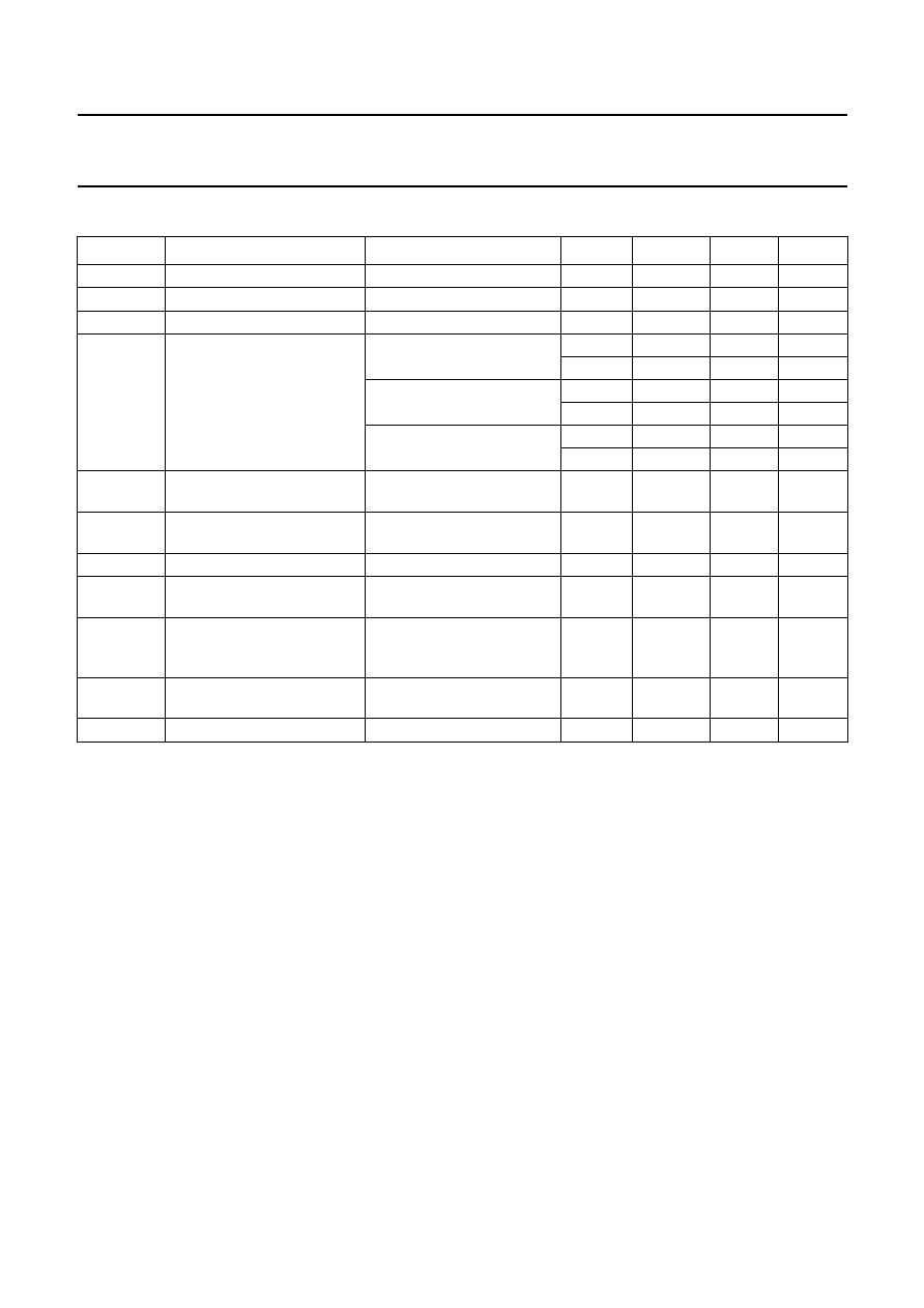
QUICK REFERENCE DATA
SYMBOL
PARAMETER
CONDITIONS
MIN.
TYP.
MAX.
UNIT
V
DD
supply voltage
4
5
5.5
V
I
DD
supply current
V
DD
= 5 V at code 0000H
-
3.4
6.0
mA
V
FS
full scale output voltage
V
DD
= 5 V
1.8
2.0
2.2
V
(THD+N)/S
total harmonic distortion
plus noise
at 0 dB signal level
-
-
68
-
63
dB
-
0.04
0.07
%
at
-
60 dB signal level
-
-
30
-
24
dB
-
3
6
%
at
-
60 dB signal level;
A-weighted
-
-
33
-
dB
-
2
-
%
S/N
signal-to-noise ratio at
bipolar zero
A-weighted at code 0000H
86
92
-
dB
t
cs
current settling time to
±
1
LSB
-
0.2
-
µ
s
BR
input bit rate at data input
-
-
18.4
Mbits/s
f
BCK
clock frequency at clock
input
-
-
18.4
MHz
TC
FS
full scale temperature
coefficient at analog outputs
(I
OL
; I
OR
)
-
±
400
-
ppm
T
amb
operating ambient
temperature
-
40
-
+85
∞
C
P
tot
total power dissipation
V
DD
= 5 V at code 0000H
-
17
30
mW
1995 Dec 18
4
Philips Semiconductors
Preliminary specification
Stereo Continuous Calibration DAC
(CC-DAC)
TDA1311A
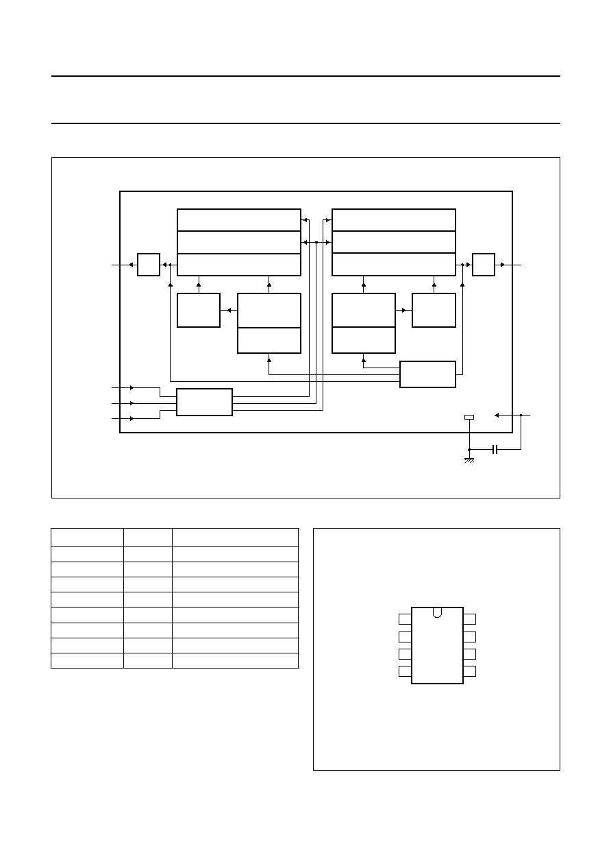
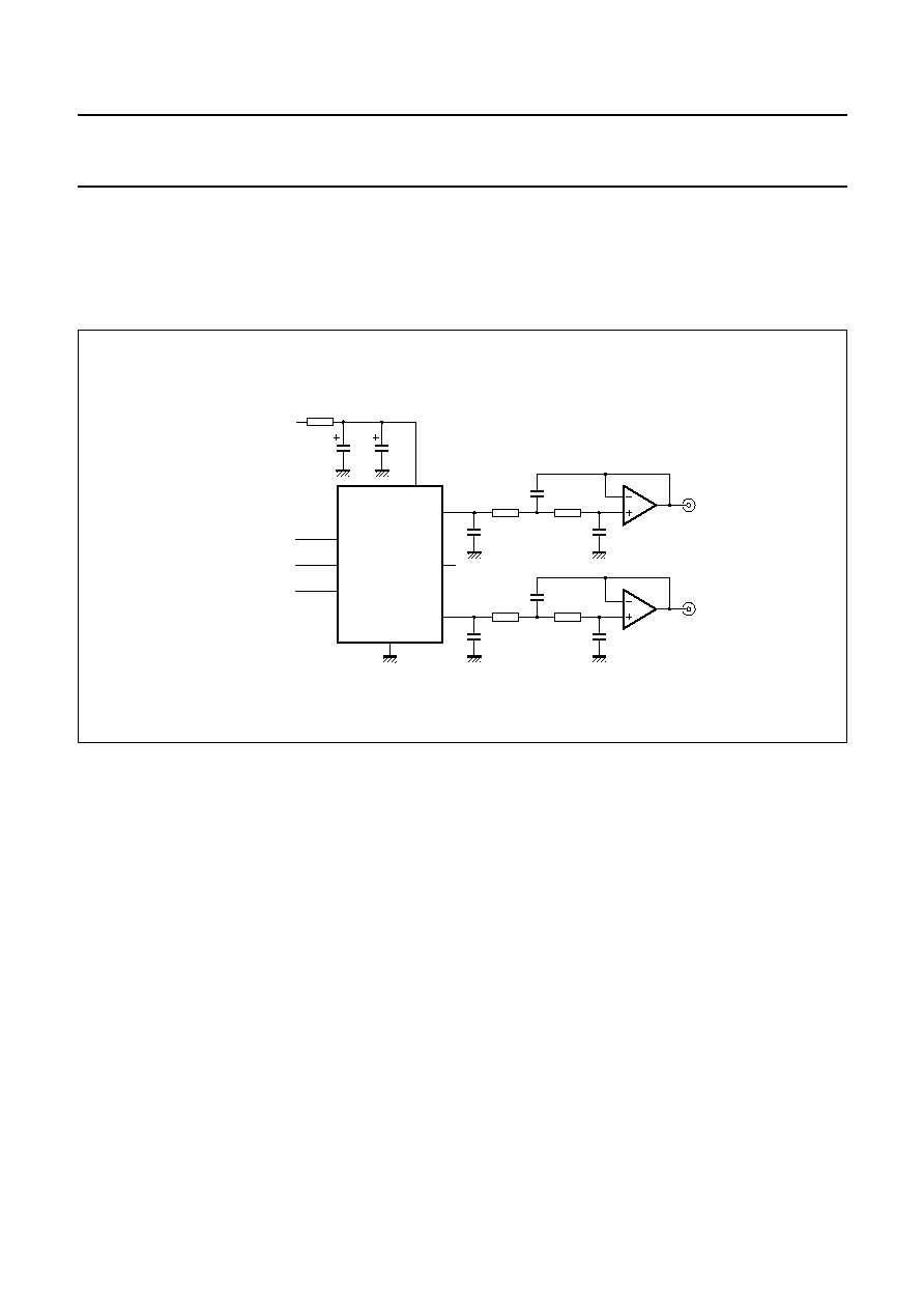
BLOCK DIAGRAM
Fig.1 Block diagram.
handbook, full pagewidth
MBG858
32 (5-BIT)
CALIBRATED
CURRENT
SOURCES
1 CALIBRATED
SPARE SOURCE
11-BIT
PASSIVE
DIVIDER
LEFT BIT SWITCHES
6
I/V
LEFT INPUT REGISTER
LEFT OUTPUT REGISTER
RIGHT BIT SWITCHES
RIGHT INPUT REGISTER
RIGHT OUTPUT REGISTER
8
I/V
32 (5-BIT)
CALIBRATED
CURRENT
SOURCES
1 CALIBRATED
SPARE SOURCE
11-BIT
PASSIVE
DIVIDER
REFERENCE
SOURCE
CONTROL
AND TIMING
1
2
3
5
4
C2
100 nF
VDD
VOR
IOR
GND
TDA1311A
TDA1311AT
VOL
BCK
WS
DATA
IOL
PINNING
SYMBOL
PIN
DESCRIPTION
BCK
1
bit clock input
WS
2
word select input
DATA
3
data input
GND
4
ground
V
DD
5
supply voltage
V
OL
6
left channel output
n.c.
7
not connected
V
OR
8
right channel output
Fig.2 Pin configuration.
handbook, halfpage
1
2
3
4
8
7
6
5
MBG859
TDA1311A
TDA1311AT
BCK
WS
DATA
GND
VDD
VOL
VOR
n.c.
1995 Dec 18
5
Philips Semiconductors
Preliminary specification
Stereo Continuous Calibration DAC
(CC-DAC)
TDA1311A
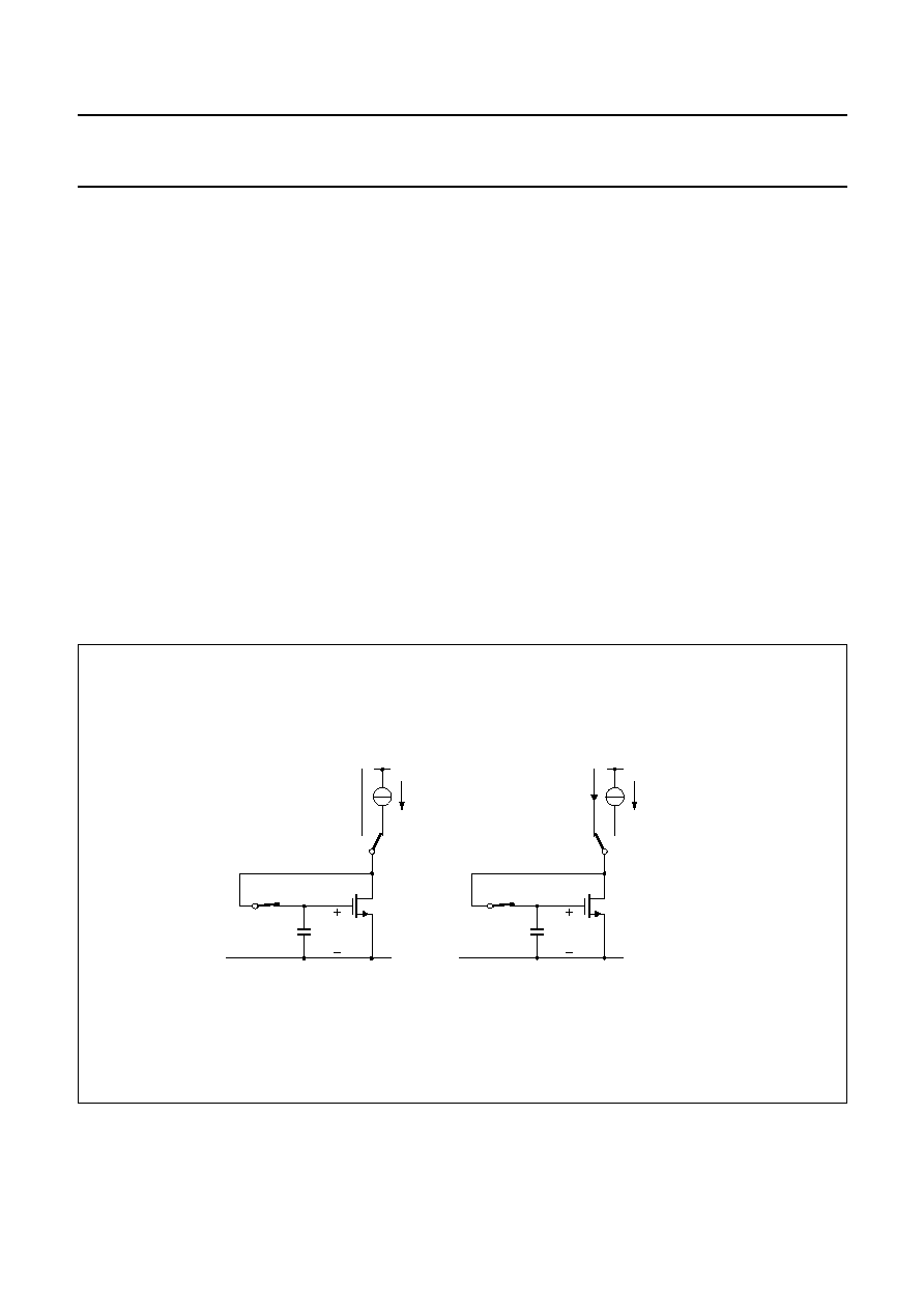
FUNCTIONAL DESCRIPTION
The basic operation of the continuous calibration DAC is
illustrated in Fig.3. The figure shows the calibration and
operation cycle. During calibration of the MOS current
source (see Fig.3a) transistor M1 is connected as a diode
by applying a reference current. The voltage V
gs
on the
intrinsic gate-source capacitance C
gs
of M1 is then
determined by the transistor characteristics. After
calibration of the drain current to the reference value I
REF
,
the switch S1 is opened and S2 is switched to the other
position (see Fig.3b). The gate-to-source voltage V
gs
of
M1 is not changed because the charge on C
gs
is
preserved. Therefore, the drain current of M1 will still be
equal to I
REF
and this exact duplicate of I
REF
is now
available at the OUT terminal.
The 32 current sources and the spare current source of the
TDA1311A; AT are continuously calibrated (see Fig.1).
The spare current source is included to allow continuous
converter operation. The output of one calibrated source is
connected to an 11-bit binary current divider consisting of
2048 transistors.
A symmetrical offset decoding principle is incorporated
that arranges the bit switching in such a way that the
zero-crossing is performed only by switching the LSB
currents.
The TDA1311A; AT (CC-DAC) accepts serial input data
formats of 16-bit word length. Left and right data words are
time multiplexed. The most significant bit (bit 1) must
always be first. The input data format is shown in Figs 4
and 5.
With a HIGH level on the word select input (WS), data is
placed in the left input register and with a LOW level on the
WS input, data is placed in the right input register (see
Fig.1). The data in the input registers are simultaneously
latched in the output registers which control the bit
switches.
An internal offset voltage V
OS
is added to the full scale
output voltage V
FS
; V
OS
and V
FS
are proportional to V
DD
:
V
DD1
/V
DD2
= V
FS1
/V
FS2
= V
OS1
/V
OS2
.
Fig.3 Calibration principle.
handbook, full pagewidth
MBG860
out
S2
S1
M1
Cgs
Vgs
Cgs
Vgs
out
S2
S1
M1
Iref
Iref
Iref
(a)
(b)
(a) = calibration.
(b) = operation.
1995 Dec 18
6
Philips Semiconductors
Preliminary specification
Stereo Continuous Calibration DAC
(CC-DAC)
TDA1311A
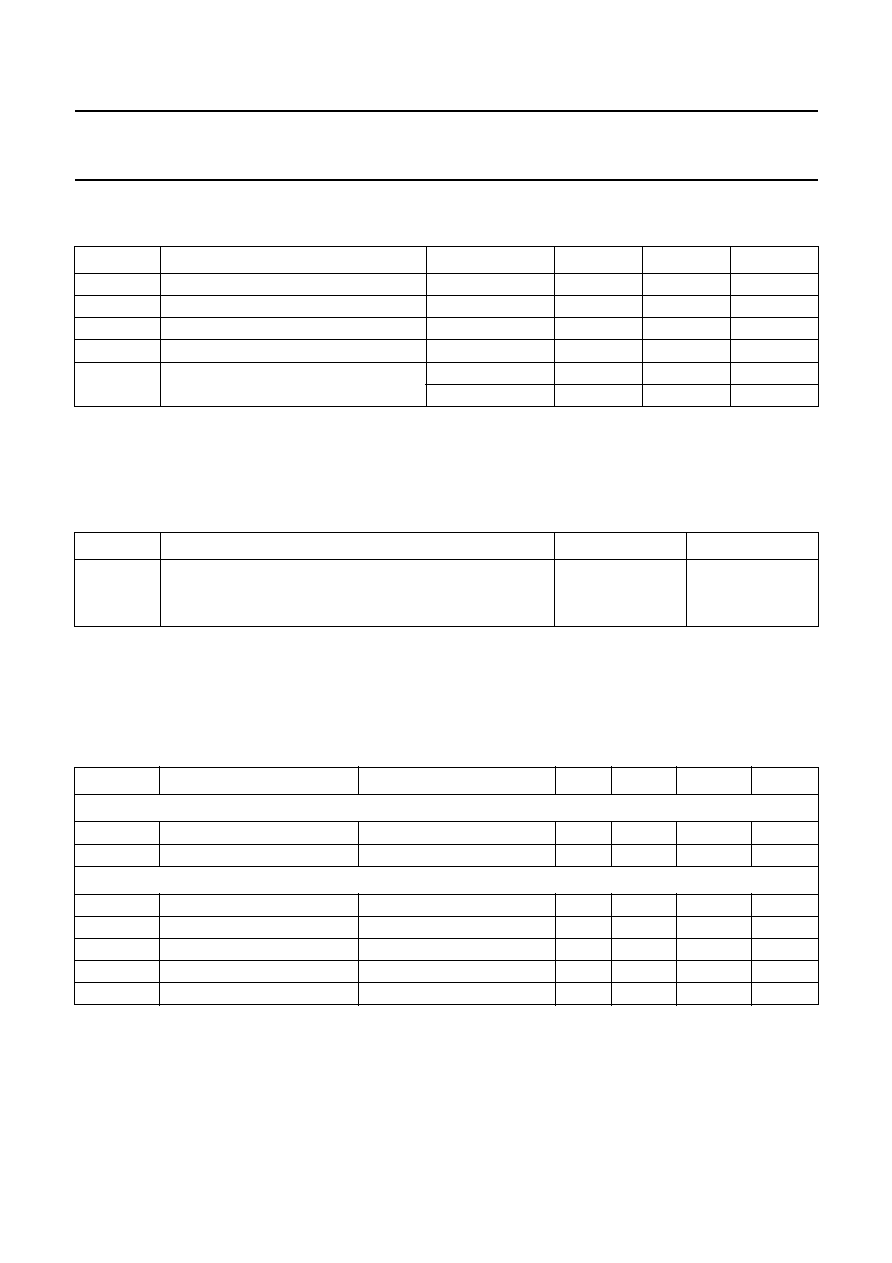
LIMITING VALUES
In accordance with the Absolute Maximum Rating System (IEC 134).
Note
1. Human body model: C = 100 pF, R = 1500
, 3 pulses positive and 3 pulses negative.
2. Machine model: C = 200 pF, L = 0.5
µ
H, R = 10
, 3 pulses positive and 3 pulses negative.
THERMAL RESISTANCE
QUALITY SPECIFICATION
In accordance with SNW-FQ-0611.
CHARACTERISTICS
V
DD
= 5 V; T
amb
= 25
∞
C; measured in Fig.1; unless otherwise specified.
SYMBOL
PARAMETER
CONDITIONS
MIN.
MAX.
UNIT
V
DD
supply voltage
-
6.0
V
T
stg
storage temperature
-
55
+150
∞
C
T
XTAL
maximum crystal temperature
-
+150
∞
C
T
amb
operating ambient temperature
-
40
+85
∞
C
V
es
electrostatic handling
note 1
-
2000
+2000
V
note 2
-
200
+200
V
SYMBOL
PARAMETER
VALUE
UNIT
R
th j-a
thermal resistance from junction to ambient in free air
DIL8
100
K/W
SO8
210
K/W
SYMBOL
PARAMETER
CONDITIONS
MIN.
TYP.
MAX.
UNIT
Supply
V
DD
supply voltage
4.0
5.0
5.5
V
I
DD
supply current
at code 0000H
-
3.4
6.0
mA
Digital inputs; pins WS, BCK and DATA
|
I
IL
|
input leakage current LOW
V
I
= 0.8 V
-
-
10
µ
A
|
I
IH
|
input leakage current HIGH
V
I
= 2.4 V
-
-
10
µ
A
f
BCK
clock frequency
-
-
18.4
MHz
BR
bit rate data input
-
-
18.4
Mbits/s
f
WS
word select input frequency
-
-
384
kHz
1995 Dec 18
7
Philips Semiconductors
Preliminary specification
Stereo Continuous Calibration DAC
(CC-DAC)
TDA1311A
Note
1. Measured with 1 kHz sinewave generated at sampling rate of 192 kHz.
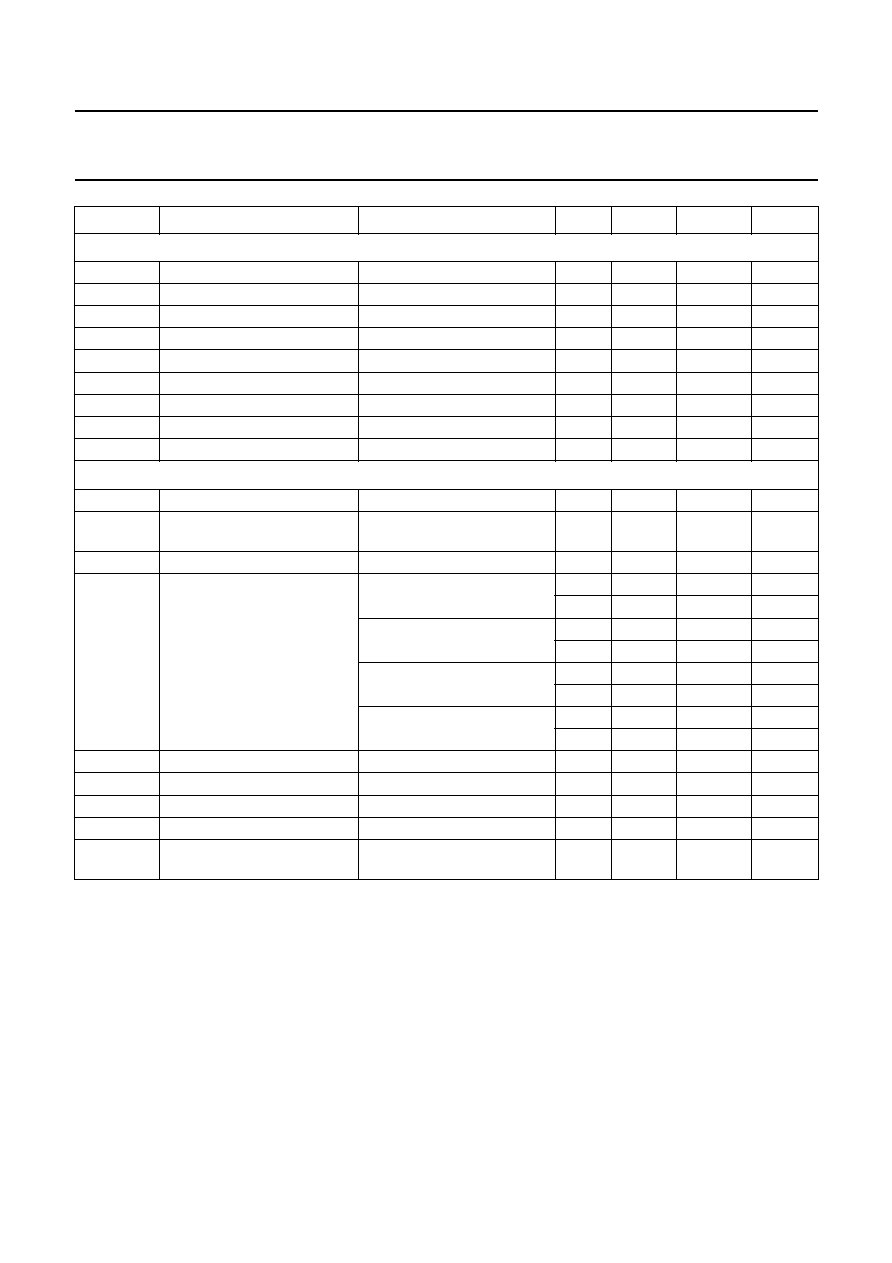
Timing (see Fig.4)
t
r
rise time
-
-
12
ns
t
f
fall time
-
-
12
ns
t
CY
bit clock cycle time
54
-
-
ns
t
BCKH
bit clock pulse width HIGH
15
-
-
ns
t
BCKL
bit clock pulse width LOW
15
-
-
ns
t
SU;DAT
data set-up time
12
-
-
ns
t
HD:DAT
data hold time to bit clock
2
-
-
ns
t
HD:WS
word select hold time
2
-
-
ns
t
SU;WS
word select set-up time
12
-
-
ns
Analog outputs; pins V
OL
and V
OR
V
FS
full-scale voltage
1.8
2.0
2.2
V
TC
FS
full-scale temperature
coefficient
-
±
400
-
ppm
V
os
offset voltage
V
DD
= V
OL/ORmax
0.45
0.50
0.55
V
(THD+N)/S
total harmonic distortion plus
noise
at 0 dB signal level; note 1
-
-
68
-
63
dB
-
0.04
0.07
%
at
-
60 dB signal level; note 1
-
-
30
-
24
dB
-
3
6
%
at
-
60 dB signal level;
A-weighted; note 1
-
-
33
-
dB
-
2
-
%
at 0 dB signal level; f = 20 Hz
to 20 kHz
-
-
65
-
61
dB
-
0.05
0.09
%
t
cs
current settling time to
±
1 LSB
-
0.2
-
µ
s
cs
channel separation
75
80
-
dB
|
I
O
|
unbalance between outputs
note 1
-
0.2
0.3
dB
|
t
d
|
time delay between outputs
-
±
0.2
-
µ
s
S/N
signal-to-noise ratio at
bipolar zero
A-weighted at code 0000H
86
92
-
dB
SYMBOL
PARAMETER
CONDITIONS
MIN.
TYP.
MAX.
UNIT
1995 Dec 18
8
Philips Semiconductors
Preliminary specification
Stereo Continuous Calibration DAC
(CC-DAC)
TDA1311A
Fig.4 Timing and input signals.
handbook, full pagewidth
MBG861
sample out
WS
BCK
DATA
RIGHT
LSB
MSB
LEFT
tHD; WS
tSU; WS
tSU; DAT
tHD; DAT
tBCKL
tBCKH
tf
tr
>
12
>
15
>
15
tCY
>
54
<
12
<
12
>
2
>
12
>
2
1995
Dec
18
9
Philips Semiconductors
Preliminary specification
Stereo Continuous Calibration DAC
(CC-DAC)
TDA131
1A
handbook, full pagewidth
MBG862
LSB
MSB
LSB
MSB
DATA
BCK
WS
LEFT
RIGHT
sample out
Fig.5 Format of input signals.
1995 Dec 18
10
Philips Semiconductors
Preliminary specification
Stereo Continuous Calibration DAC
(CC-DAC)
TDA1311A
APPLICATION INFORMATION
Basic application example
A typical example of a CD-application with the TDA1311A; AT is shown in Fig.6. It features typical decoupling
components and a third-order analog post-filter stage providing a line output.
Fig.6 Example of a 3rd order filter application.
handbook, full pagewidth
100 pF
22 k
420 pF
22 k
2.2 nF
TDA1311A
TDA1311AT
5
8
7
6
4
1
2
3
BCK
WS
DATA
100 pF
22 k
420 pF
22 k
2.2 nF
100
nF
47
µ
F
VDD
10
MBG863
Attention to printed circuit board layout
The TDA1311A and even more so the TDA1311AT offers
great ease in designing-in to printed-circuit boards due to
its small size and low pin count. The TDA1311A; AT being
a mixed-signal IC in CMOS, some attention needs to be
paid to layout and topology of the application PCB.
Following some basic rules will yield the desired
performance. The most important considerations are:
1. Supply: care should be taken to supply the
TDA1311A; AT with a clean, noiseless V
DD
, for a good
noise performance of the analog parts of the DAC.
Supply purity can easily be achieved by using an
RC-filtered supply.
2. Grounding: preferably a ground plane should be used,
in order to have a low-impedance return available at
any point in the layout. It is advantageous to make a
partitioning of the ground plane according to the nature
of the expected return currents (digital input returns
separate from supply returns and separate from the
analog section).
3. Topology: the capacitor decoupling high-frequency
supply interference from V
DD
to GND should be placed
as close as is physically possible to the IC body,
ensuring a low-inductance path to ground. The digital
input conductors may be shielded by ground leads
running alongside. The placement of a passive ground
plane underside the entire IC surface gives `free`
additional decoupling from the IC body to ground as
well as providing a shield between the digital input pins
and the analog output pins.
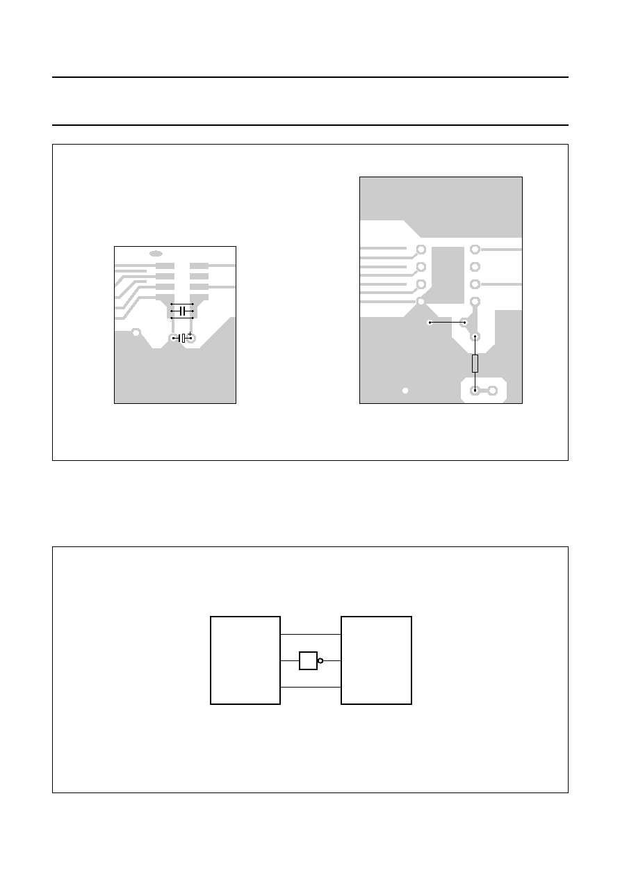
Figure 7 shows recommended layouts for printed-circuit
boards for the SO8 and DIL8 versions respectively. Both
layouts use a single-interconnect layer.
1995 Dec 18
11
Philips Semiconductors
Preliminary specification
Stereo Continuous Calibration DAC
(CC-DAC)
TDA1311A
Fig.7 Recommended printed-circuit board layouts.
handbook, full pagewidth
MSA739
V DD
R
V DD
C1
C2
Interface examples
The following figures (Figs 8 to 14) show examples of connections to commonly used decoder and digital filter ICs. The
digital interface part is shown only, for clarity. The diagrams are for guidance purposes only - no guarantee for industrial
exploitation is implied.
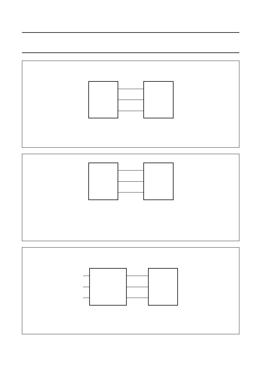
Fig.8 NPC SM5807 digital filter (4FS).
handbook, halfpage
SM5807
15
BCKO
14
LRCOn
12
DOUT
TDA1311A
TDA1311AT
1
BCK
2
WS
3
DATA
1
remark: SCSLn
-
signal SM5807 both "L" and "H" supported
by TDA1311A and TDA1311AT
MBG864
1995 Dec 18
12
Philips Semiconductors
Preliminary specification
Stereo Continuous Calibration DAC
(CC-DAC)
TDA1311A
Fig.9 NPC SM5840 digital filter (4FS).
handbook, halfpage
SM5840
(1)
14
DOL
13
DOR
12
BCKO
TDA1311A
TDA1311AT
1
BCK
2
WS
3
DATA
OMODn pin 19: "L" for 4FS operation
(1)
versions A/B/G
MBG865
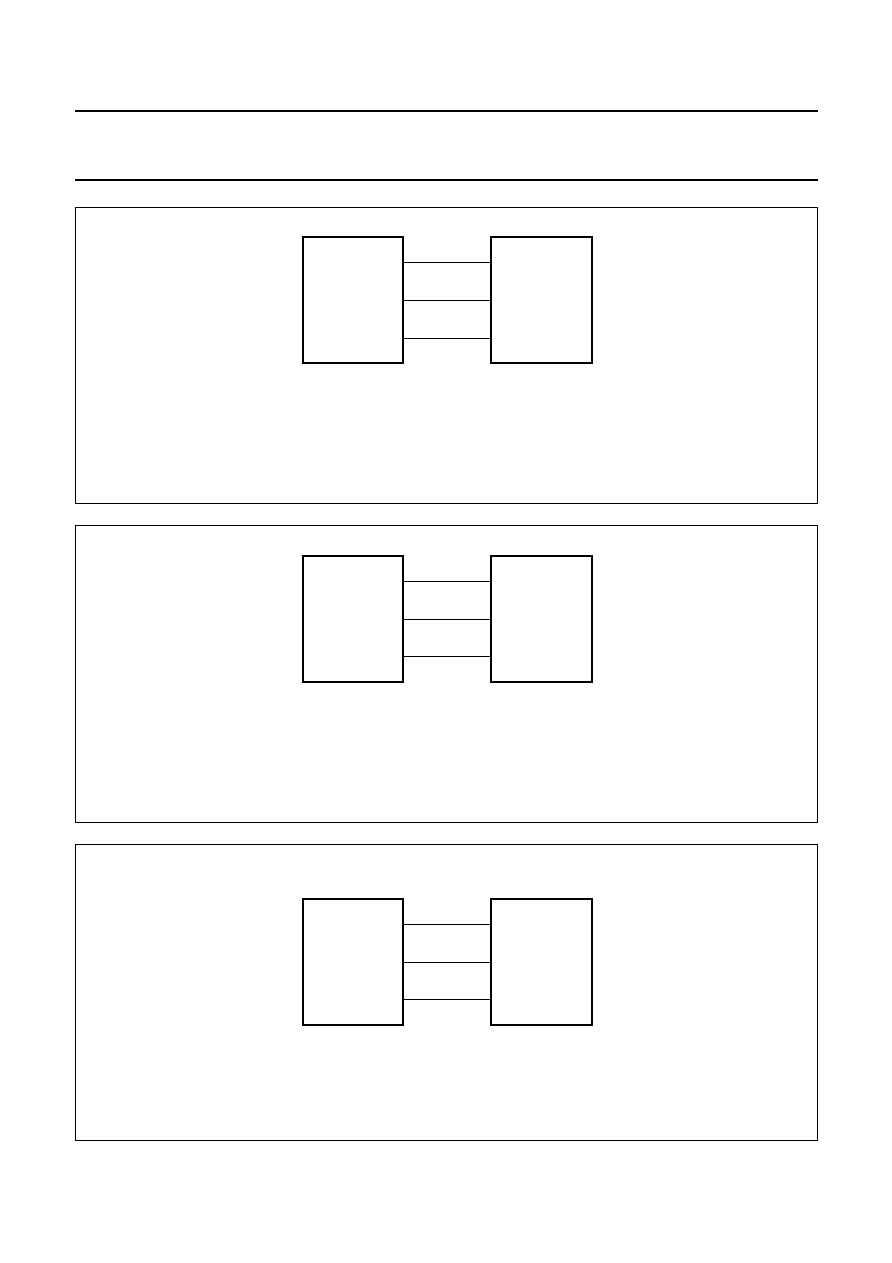
Fig.10 Sony CXD1125 decoder (1FS).
handbook, halfpage
CXD1125
76
C2IOn
80
LRCK
78
DATA
TDA1311A
TDA1311AT
1
BCK
2
WS
3
DATA
MODE SELECT:
MD1 pin 55: "L"
MD2 pin 56: "L" to use DOTX function
MD3 pin 57: "H"
PSSL pin 59: "L"
SLOB pin 58: "L"
MBG866
Fig.11 Sony CXD1162 digital filter (4FS).
handbook, halfpage
CXD1125
3
C2IOn
1
LRD
4
DATA
TDA1311A
TDA1311AT
1
BCK
2
WS
3
9
7
8
DATA
BCK
LRCK
DATA
remark: CXD1162 input connectable to CXD1125
in the same way as for TDA1311A; AT to CXD1125
MBG867
1995 Dec 18
13
Philips Semiconductors
Preliminary specification
Stereo Continuous Calibration DAC
(CC-DAC)
TDA1311A
Fig.12 Sony CXD1135 decoder (1FS) and digital filter (2FS).
handbook, halfpage
CXD1135
76
DA14
80
LRCK
78
DA16
TDA1311A
TDA1311AT
1
BCK
2
WS
3
DATA
MODE SELECT:
MD1 pin 55: "L"
MD2 pin 56: "L" to use DOTX function
MD3 pin 57: "H" for 1FS; "L" for 2FS
PSSL pin 59: "L"
SLOB pin 58: "L"
MBG868
Fig.13 Mitsubishi M50423 decoder (1FS) and digital filter (4FS).
handbook, halfpage
M50423
74
DSCK
75
LRCK
72
DO1
TDA1311A
TDA1311AT
1
BCK
2
WS
3
DATA
MODE SELECT:
DOBSEL pin 7: "L"
DASEL1 pin 8: "H"
DASEL2 pin 9: "L"
DASEL3 pin 10: "H"
DASEL4 pin 11: "L"
MBG869
Fig.14 Sanyo LC7863 decoder (1FS).
handbook, halfpage
LC7863
35
DACLK
30
LRCLK
34
DFOUT
TDA1311A
TDA1311AT
1
BCK
2
WS
3
DATA
MODE SELECT:
DFOFF pin 27: "L"
MSBF pin 38: "H"
MBG870
1995 Dec 18
14
Philips Semiconductors
Preliminary specification
Stereo Continuous Calibration DAC
(CC-DAC)
TDA1311A
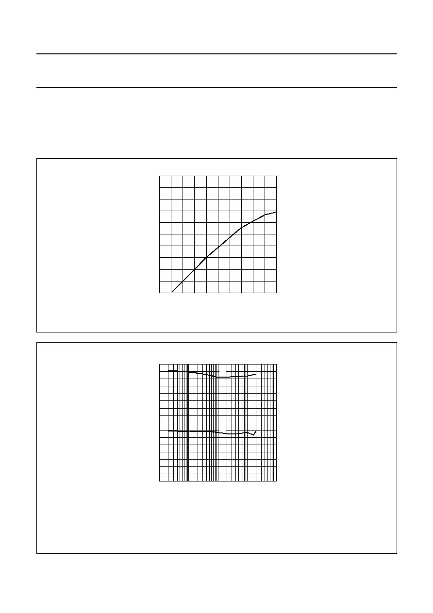
Evaluation of audio parameters
The following measurement graphs are performed on singular engineering samples; therefore no guarantee of typical
parameter values is implied. Measurement conditions are typical, as stated in the section Characteristics, unless
otherwise indicated. The normal measurement set-up includes a 20 kHz band-limiting filter for bandwidth definition, and
an A-weighting filter where indicated.
Fig.15 Total harmonic distortion plus noise as a function of signal level (4FS).
handbook, halfpage
-
100
-
80
-
60
-
40
-
20
0
THD
(dB)
signal level (dB)
-
100
-
80
-
60
-
40
-
20
0
MBG871
Fig.16 Total harmonic distortion plus noises as a function of frequency (4FS).
(1) Measured including all distortion plus noise at a signal level of
-
60 dB.
(2) Measured including all distortion plus noise at a signal level of 0 dB.
handbook, halfpage
MBG873
10
2
10
3
10
4
10
5
10
frequency (Hz)
THD
(dB)
THD
(%)
-
20
10
1
0.1
0.01
0.001
-
40
-
60
-
80
-
100
(1)
(2)
1995 Dec 18
15
Philips Semiconductors
Preliminary specification
Stereo Continuous Calibration DAC
(CC-DAC)
TDA1311A
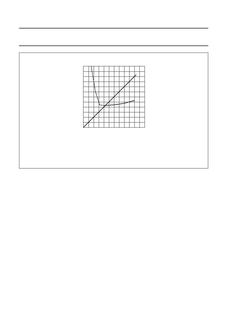
Fig.17 Total harmonic distortion plus noise as a function of supply voltage (4FS).
(1) Measured including all distortion plus noise within the specified operating supply voltage range.
(2) Measured including all distortion plus noise outside the specified operating supply voltage range.
(3) V
FS
relative to nominal.
handbook, halfpage
3
THD
(dB)
THD
(%)
4
6
VDD (V)
-
50
-
60
-
70
-
80
20
0
-
20
-
40
MBG872
5
(1)
(3)
(2)
1995 Dec 18
16
Philips Semiconductors
Preliminary specification
Stereo Continuous Calibration DAC
(CC-DAC)
TDA1311A
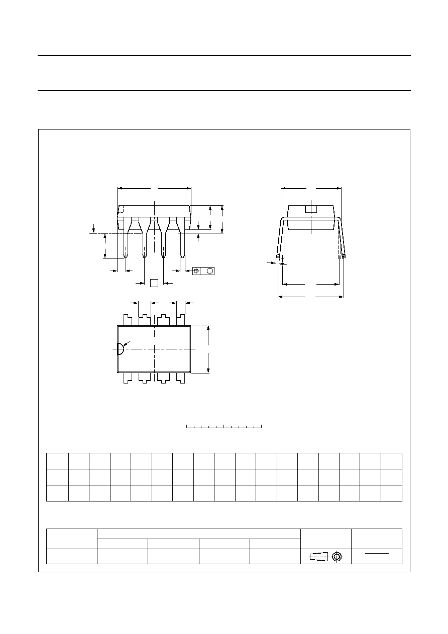
PACKAGE OUTLINES
REFERENCES
OUTLINE
VERSION
EUROPEAN
PROJECTION
ISSUE DATE
IEC
JEDEC
EIAJ
SOT97-1
92-11-17
95-02-04
UNIT
A
max.
1
2
b
1
(1)
(1)
(1)
b
2
c
D
E
e
M
Z
H
L
mm
DIMENSIONS (inch dimensions are derived from the original mm dimensions)
A
min.
A
max.
b
max.
w
M
E
e
1
1.73
1.14
0.53
0.38
0.36
0.23
9.8
9.2
6.48
6.20
3.60
3.05
0.254
2.54
7.62
8.25
7.80
10.0
8.3
1.15
4.2
0.51
3.2
inches
0.068
0.045
0.021
0.015
0.014
0.009
1.07
0.89
0.042
0.035
0.39
0.36
0.26
0.24
0.14
0.12
0.01
0.10
0.30
0.32
0.31
0.39
0.33
0.045
0.17
0.020
0.13
b
2
050G01
MO-001AN
M
H
c
(e )
1
M
E
A
L
seating plane
A
1
w
M
b
1
e
D
A
2
Z
8
1
5
4
b
E
0
5
10 mm
scale
Note
1. Plastic or metal protrusions of 0.25 mm maximum per side are not included.
pin 1 index
DIP8: plastic dual in-line package; 8 leads (300 mil)
SOT97-1
1995 Dec 18
17
Philips Semiconductors
Preliminary specification
Stereo Continuous Calibration DAC
(CC-DAC)
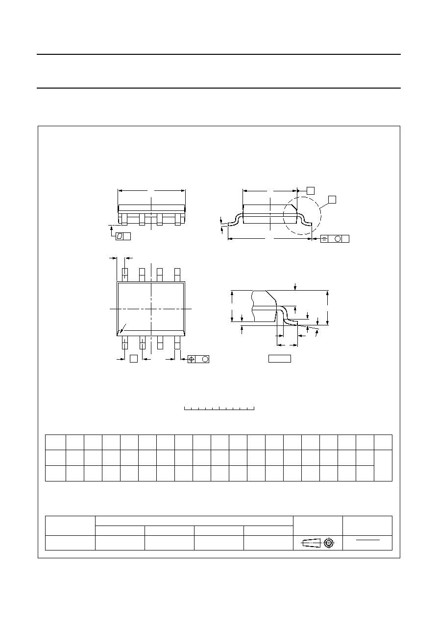
TDA1311A
UNIT
A
max.
A
1
A
2
A
3
b
p
c
D
(1)
E
(2)
(1)
e
H
E
L
L
p
Q
Z
y
w
v
REFERENCES
OUTLINE
VERSION
EUROPEAN
PROJECTION
ISSUE DATE
IEC
JEDEC
EIAJ
mm
inches
1.75
0.25
0.10
1.45
1.25
0.25
0.49
0.36
0.25
0.19
5.0
4.8
4.0
3.8
1.27
6.2
5.8
1.05
0.7
0.6
0.7
0.3
8
0
o
o
0.25
0.1
0.25
DIMENSIONS (inch dimensions are derived from the original mm dimensions)
Notes
1. Plastic or metal protrusions of 0.15 mm maximum per side are not included.
2. Plastic or metal protrusions of 0.25 mm maximum per side are not included.
1.0
0.4
SOT96-1
X
w
M
A
A
1
A
2
b
p
D
H
E
L
p
Q
detail X
E
Z
e
c
L
v
M
A
(A )
3
A
4
5
pin 1 index
1
8
y
076E03S
MS-012AA
0.069
0.010
0.004
0.057
0.049
0.01
0.019
0.014
0.0100
0.0075
0.20
0.19
0.16
0.15
0.050
0.244
0.228
0.028
0.024
0.028
0.012
0.01
0.01
0.041
0.004
0.039
0.016
0
2.5
5 mm
scale
SO8: plastic small outline package; 8 leads; body width 3.9 mm
SOT96-1
95-02-04
97-05-22

1995 Dec 18
18
Philips Semiconductors
Preliminary specification
Stereo Continuous Calibration DAC
(CC-DAC)
TDA1311A
SOLDERING
Introduction
There is no soldering method that is ideal for all IC
packages. Wave soldering is often preferred when
through-hole and surface mounted components are mixed
on one printed-circuit board. However, wave soldering is
not always suitable for surface mounted ICs, or for
printed-circuits with high population densities. In these
situations reflow soldering is often used.
This text gives a very brief insight to a complex technology.
A more in-depth account of soldering ICs can be found in
our
"IC Package Databook" (order code 9398 652 90011).
DIP
S
OLDERING BY DIPPING OR BY WAVE
The maximum permissible temperature of the solder is
260
∞
C; solder at this temperature must not be in contact
with the joint for more than 5 seconds. The total contact
time of successive solder waves must not exceed
5 seconds.
The device may be mounted up to the seating plane, but
the temperature of the plastic body must not exceed the
specified maximum storage temperature (T
stg max
). If the
printed-circuit board has been pre-heated, forced cooling
may be necessary immediately after soldering to keep the
temperature within the permissible limit.
R
EPAIRING SOLDERED JOINTS
Apply a low voltage soldering iron (less than 24 V) to the
lead(s) of the package, below the seating plane or not
more than 2 mm above it. If the temperature of the
soldering iron bit is less than 300
∞
C it may remain in
contact for up to 10 seconds. If the bit temperature is
between 300 and 400
∞
C, contact may be up to 5 seconds.
SO
R
EFLOW SOLDERING
Reflow soldering techniques are suitable for all SO
packages.
Reflow soldering requires solder paste (a suspension of
fine solder particles, flux and binding agent) to be applied
to the printed-circuit board by screen printing, stencilling or
pressure-syringe dispensing before package placement.
Several techniques exist for reflowing; for example,
thermal conduction by heated belt. Dwell times vary
between 50 and 300 seconds depending on heating
method. Typical reflow temperatures range from
215 to 250
∞
C.
Preheating is necessary to dry the paste and evaporate
the binding agent. Preheating duration: 45 minutes at
45
∞
C.
W
AVE SOLDERING
Wave soldering techniques can be used for all SO
packages if the following conditions are observed:
∑
A double-wave (a turbulent wave with high upward
pressure followed by a smooth laminar wave) soldering
technique should be used.
∑
The longitudinal axis of the package footprint must be
parallel to the solder flow.
∑
The package footprint must incorporate solder thieves at
the downstream end.
During placement and before soldering, the package must
be fixed with a droplet of adhesive. The adhesive can be
applied by screen printing, pin transfer or syringe
dispensing. The package can be soldered after the
adhesive is cured.
Maximum permissible solder temperature is 260
∞
C, and
maximum duration of package immersion in solder is
10 seconds, if cooled to less than 150
∞
C within
6 seconds. Typical dwell time is 4 seconds at 250
∞
C.
A mildly-activated flux will eliminate the need for removal
of corrosive residues in most applications.
R
EPAIRING SOLDERED JOINTS
Fix the component by first soldering two diagonally-
opposite end leads. Use only a low voltage soldering iron
(less than 24 V) applied to the flat part of the lead. Contact
time must be limited to 10 seconds at up to 300
∞
C. When
using a dedicated tool, all other leads can be soldered in
one operation within 2 to 5 seconds between
270 and 320
∞
C.

1995 Dec 18
19
Philips Semiconductors
Preliminary specification
Stereo Continuous Calibration DAC
(CC-DAC)
TDA1311A
DEFINITIONS
LIFE SUPPORT APPLICATIONS
These products are not designed for use in life support appliances, devices, or systems where malfunction of these
products can reasonably be expected to result in personal injury. Philips customers using or selling these products for
use in such applications do so at their own risk and agree to fully indemnify Philips for any damages resulting from such
improper use or sale.
Data sheet status
Objective specification
This data sheet contains target or goal specifications for product development.
Preliminary specification
This data sheet contains preliminary data; supplementary data may be published later.
Product specification
This data sheet contains final product specifications.
Limiting values
Limiting values given are in accordance with the Absolute Maximum Rating System (IEC 134). Stress above one or
more of the limiting values may cause permanent damage to the device. These are stress ratings only and operation
of the device at these or at any other conditions above those given in the Characteristics sections of the specification
is not implied. Exposure to limiting values for extended periods may affect device reliability.
Application information
Where application information is given, it is advisory and does not form part of the specification.

Philips Semiconductors ≠ a worldwide company
Argentina: IEROD, Av. Juramento 1992 - 14.b, (1428)
BUENOS AIRES, Tel. (541)786 7633, Fax. (541)786 9367
Australia: 34 Waterloo Road, NORTH RYDE, NSW 2113,
Tel. (02)805 4455, Fax. (02)805 4466
Austria: Triester Str. 64, A-1101 WIEN, P.O. Box 213,
Tel. (01)60 101-1236, Fax. (01)60 101-1211
Belgium: Postbus 90050, 5600 PB EINDHOVEN, The Netherlands,
Tel. (31)40-2783749, Fax. (31)40-2788399
Brazil: Rua do Rocio 220 - 5
th
floor, Suite 51,
CEP: 04552-903-S√O PAULO-SP, Brazil,
P.O. Box 7383 (01064-970),
Tel. (011)821-2333, Fax. (011)829-1849
Canada: PHILIPS SEMICONDUCTORS/COMPONENTS:
Tel. (800) 234-7381, Fax. (708) 296-8556
Chile: Av. Santa Maria 0760, SANTIAGO,
Tel. (02)773 816, Fax. (02)777 6730
China/Hong Kong: 501 Hong Kong Industrial Technology Centre,
72 Tat Chee Avenue, Kowloon Tong, HONG KONG,
Tel. (852)2319 7888, Fax. (852)2319 7700
Colombia: IPRELENSO LTDA, Carrera 21 No. 56-17,
77621 BOGOTA, Tel. (571)249 7624/(571)217 4609,
Fax. (571)217 4549
Denmark: Prags Boulevard 80, PB 1919, DK-2300
COPENHAGEN S, Tel. (45)32 88 26 36, Fax. (45)31 57 19 49
Finland: Sinikalliontie 3, FIN-02630 ESPOO,
Tel. (358)0-615 800, Fax. (358)0-61580 920
France: 4 Rue du Port-aux-Vins, BP317,
92156 SURESNES Cedex,
Tel. (01)4099 6161, Fax. (01)4099 6427
Germany: P.O. Box 10 51 40, 20035 HAMBURG,
Tel. (040)23 53 60, Fax. (040)23 53 63 00
Greece: No. 15, 25th March Street, GR 17778 TAVROS,
Tel. (01)4894 339/4894 911, Fax. (01)4814 240
India: Philips INDIA Ltd, Shivsagar Estate, A Block,
Dr. Annie Besant Rd. Worli, Bombay 400 018
Tel. (022)4938 541, Fax. (022)4938 722
Indonesia: Philips House, Jalan H.R. Rasuna Said Kav. 3-4,
P.O. Box 4252, JAKARTA 12950,
Tel. (021)5201 122, Fax. (021)5205 189
Ireland: Newstead, Clonskeagh, DUBLIN 14,
Tel. (01)7640 000, Fax. (01)7640 200
Italy: PHILIPS SEMICONDUCTORS S.r.l.,
Piazza IV Novembre 3, 20124 MILANO,
Tel. (0039)2 6752 2531, Fax. (0039)2 6752 2557
Japan: Philips Bldg 13-37, Kohnan 2 -chome, Minato-ku, TOKYO 108,
Tel. (03)3740 5130, Fax. (03)3740 5077
Korea: Philips House, 260-199 Itaewon-dong,
Yongsan-ku, SEOUL, Tel. (02)709-1412, Fax. (02)709-1415
Malaysia: No. 76 Jalan Universiti, 46200 PETALING JAYA,
SELANGOR, Tel. (03)750 5214, Fax. (03)757 4880
Mexico: 5900 Gateway East, Suite 200, EL PASO, TX 79905,
Tel. 9-5(800)234-7381, Fax. (708)296-8556
Netherlands: Postbus 90050, 5600 PB EINDHOVEN, Bldg. VB,
Tel. (040)2783749, Fax. (040)2788399
New Zealand: 2 Wagener Place, C.P.O. Box 1041, AUCKLAND,
Tel. (09)849-4160, Fax. (09)849-7811
Norway: Box 1, Manglerud 0612, OSLO,
Tel. (022)74 8000, Fax. (022)74 8341
Pakistan: Philips Electrical Industries of Pakistan Ltd.,
Exchange Bldg. ST-2/A, Block 9, KDA Scheme 5, Clifton,
KARACHI 75600, Tel. (021)587 4641-49,
Fax. (021)577035/5874546
Philippines: PHILIPS SEMICONDUCTORS PHILIPPINES Inc.,
106 Valero St. Salcedo Village, P.O. Box 2108 MCC, MAKATI,
Metro MANILA, Tel. (63) 2 816 6380, Fax. (63) 2 817 3474
Portugal: PHILIPS PORTUGUESA, S.A.,
Rua dr. AntÛnio Loureiro Borges 5, Arquiparque - Miraflores,
Apartado 300, 2795 LINDA-A-VELHA,
Tel. (01)4163160/4163333, Fax. (01)4163174/4163366
Singapore: Lorong 1, Toa Payoh, SINGAPORE 1231,
Tel. (65)350 2000, Fax. (65)251 6500
South Africa: S.A. PHILIPS Pty Ltd.,
195-215 Main Road Martindale, 2092 JOHANNESBURG,
P.O. Box 7430, Johannesburg 2000,
Tel. (011)470-5911, Fax. (011)470-5494
Spain: Balmes 22, 08007 BARCELONA,
Tel. (03)301 6312, Fax. (03)301 42 43
Sweden: Kottbygatan 7, Akalla. S-164 85 STOCKHOLM,
Tel. (0)8-632 2000, Fax. (0)8-632 2745
Switzerland: Allmendstrasse 140, CH-8027 ZÐRICH,
Tel. (01)488 2211, Fax. (01)481 77 30
Taiwan: PHILIPS TAIWAN Ltd., 23-30F, 66, Chung Hsiao West
Road, Sec. 1. Taipeh, Taiwan ROC, P.O. Box 22978,
TAIPEI 100, Tel. (886) 2 382 4443, Fax. (886) 2 382 4444
Thailand: PHILIPS ELECTRONICS (THAILAND) Ltd.,
209/2 Sanpavuth-Bangna Road Prakanong,
Bangkok 10260, THAILAND,
Tel. (66) 2 745-4090, Fax. (66) 2 398-0793
Turkey: Talatpasa Cad. No. 5, 80640 GÐLTEPE/ISTANBUL,
Tel. (0 212)279 27 70, Fax. (0212)282 67 07
Ukraine: Philips UKRAINE, 2A Akademika Koroleva str., Office 165,
252148 KIEV, Tel. 380-44-4760297, Fax. 380-44-4766991
United Kingdom: Philips Semiconductors LTD.,
276 Bath Road, Hayes, MIDDLESEX UB3 5BX,
Tel. (0181)730-5000, Fax. (0181)754-8421
United States: 811 East Arques Avenue, SUNNYVALE,
CA 94088-3409, Tel. (800)234-7381, Fax. (708)296-8556
Uruguay: Coronel Mora 433, MONTEVIDEO,
Tel. (02)70-4044, Fax. (02)92 0601
Internet: http://www.semiconductors.philips.com/ps/
For all other countries apply to: Philips Semiconductors,
International Marketing and Sales, Building BE-p,
P.O. Box 218, 5600 MD EINDHOVEN, The Netherlands,
Telex 35000 phtcnl, Fax. +31-40-2724825
SCD47
© Philips Electronics N.V. 1995
All rights are reserved. Reproduction in whole or in part is prohibited without the
prior written consent of the copyright owner.
The information presented in this document does not form part of any quotation
or contract, is believed to be accurate and reliable and may be changed without
notice. No liability will be accepted by the publisher for any consequence of its
use. Publication thereof does not convey nor imply any license under patent- or
other industrial or intellectual property rights.
Printed in The Netherlands
513061/50/02/pp20
Date of release: 1995 Dec 18
Document order number:
9397 750 00532