 | –≠–ª–µ–∫—Ç—Ä–æ–Ω–Ω—ã–π –∫–æ–º–ø–æ–Ω–µ–Ω—Ç: TDA1388 | –°–∫–∞—á–∞—Ç—å:  PDF PDF  ZIP ZIP |
Document Outline
- FEATURES
- Multiple format input interface
- Extensive channel manipulation features
- Digital sound processing
- Advanced audio output configuration
- General
- GENERAL DESCRIPTION
- ORDERING INFORMATION
- QUICK REFERENCE DATA
- BLOCK DIAGRAM
- PINNING
- FUNCTIONAL DESCRIPTION
- System clock
- Multiple format input interface
- Input mode
- Flat/min/max setting selection
- Channel manipulation modes
- De-emphasis
- Volume control
- Bass boost
- Treble
- Soft mute
- Oversampling and noise shaper
- Continuous calibration DAC
- Stereo line driver
- Stereo headphone driver
- LIMITING VALUES
- THERMAL CHARACTERISTICS
- DC CHARACTERISTICS
- AC CHARACTERISTICS (ANALOG)
- AC CHARACTERISTICS (DIGITAL)
- TEST AND APPLICATION INFORMATION
- PACKAGE OUTLINES
- SOLDERING
- DEFINITIONS
- LIFE SUPPORT APPLICATIONS

DATA SHEET
Objective specification
Supersedes data of 1995 Dec 08
File under Integrated Circuits, IC01
1996 Jul 17
INTEGRATED CIRCUITS
TDA1388
Bitstream continuous calibration
filter-DAC for CD-ROM audio
applications

1996 Jul 17
2
Philips Semiconductors
Objective specification
Bitstream continuous calibration filter-DAC
for CD-ROM audio applications
TDA1388
FEATURES
Multiple format input interface
∑
I
2
S-bus and LSB-justified input format compatible
∑
1f
s
input format data rate.
Extensive channel manipulation features
∑
Separate soft mute on left and right channel
∑
Channel interchange function (left to right and right to
left)
∑
Monaural function (left to right or right to left)
∑
True mono function
1
/
2
(left plus right).
Digital sound processing
∑
Separate digital volume control for left and right
channels
∑
Digital tone control, bass boost and treble
∑
dB-linear volume and tone control (low microcontroller
load)
∑
Digital de-emphasis
∑
Soft mute.
Advanced audio output configuration
∑
Stereo line output (under microcontroller volume
control)
∑
Stereo headphone output (under 5-tap potentiometer
volume control)
∑
Line output independent of headphone output volume
∑
Power on/off click prevention circuitry
∑
High linearity, dynamic range, low distortion.
General
∑
Integrated digital filter plus DAC plus headphone driver
∑
No analog post filter required
∑
Easy application
∑
Functions controllable by static pins or by
microcontroller interface
∑
5 V power supply
∑
Low power consumption
∑
Small package size (SO28 and SSOP28).
GENERAL DESCRIPTION
The TDA1388 CMOS digital-to-analog bitstream converter
incorporates an up-sampling digital filter and noise shaper,
unique signal processing features and integrated line and
headphone drivers. The digital processing features are of
high sound quality due to the wide dynamic range of the
bitstream conversion technique.
The TDA1388 supports the I
2
S-bus data input mode with
word lengths of up to 20 bits and the LSB justified serial
data input format with word lengths of 16, 18 and 20 bits.
Two cascaded half-band filters and a sample-and-hold
function increase the oversampling rate from 1f
s
to 64f
s
.
A 2nd-order noise shaper converts this oversampled data
to a bitstream for the 5-bit continuous calibration
Digital-to-Analog Converters (DACs).
On board amplifiers convert the output current to a voltage
signal capable of driving a line output. The signal is also
used to feed the integrated headphone amplifiers.
The volume of the headphone is controlled by an external
potentiometer.
The TDA1388 has special sound processing features for
use in CD-ROM audio applications, which can be
controlled by static pins or microcontroller interface.
These functions are de-emphasis, volume, bass boost,
treble, soft mute and the channel manipulation functions
needed for ATAPI-compliant functionality in CD-ROM
audio processing.
1996 Jul 17
3
Philips Semiconductors
Objective specification
Bitstream continuous calibration filter-DAC
for CD-ROM audio applications
TDA1388
ORDERING INFORMATION
QUICK REFERENCE DATA
Notes
1. All V
DD
and V
SS
pins must be connected to the same supply or ground respectively.
2. Measured at input code 00000H and V
DD
= 5 V.
TYPE
NUMBER
PACKAGE
NAME
DESCRIPTION
VERSION
TDA1388T
SO28
plastic small outline package; 28 leads; body width 7.5 mm.
SOT136-1
TDA1388M
SSOP28
plastic shrink small outline package; 28 leads; body width 5.3 mm.
SOT341-1
SYMBOL
PARAMETER
CONDITIONS
MIN.
TYP.
MAX.
UNIT
Supply
V
DD
supply voltage
note 1
4.5
5.0
5.5
V
I
DD
supply current
note 2
-
22
-
mA
V
FS(rms)
full-scale output voltage
(RMS value)
V
DD
= 5 V
0.9
1.0
1.1
V
(THD+N)/S
total harmonic distortion plus
noise as a function of signal for
the line output
0 dB signal;
R
L
= 5 k
-
-
85
-
80
dB
-
0.006
0.013
%
-
60 dB signal;
R
L
= 5 k
-
-
35
-
30
dBA
-
1.8
3.2
%
total harmonic distortion plus
noise as a function of signal for
the headphone output
0 dB signal;
R
L
= 16
-
-
65
-
dB
-
0.056
-
%
0 dB signal;
R
L
= 32
-
-
70
-
dB
-
0.032
-
%
-
60 dB signal;
R
L
= 16
or R
L
= 32
-
-
35
-
30
dBA
-
1.8
3.2
%
S/N
signal-to-noise ratio
A-weighted;
at code 00000H
90
95
-
dBA
BR
input bit rate at data input
f
sys
= 256f
s
-
64f
s
-
bits
f
sys
= 384f
s
-
48f
s
-
bits
f
sys
system clock frequency
8.192
-
18.432
MHz
T
amb
operating ambient temperature
-
20
-
+70
∞
C

1996 Jul 17
4
Philips Semiconductors
Objective specification
Bitstream continuous calibration filter-DAC
for CD-ROM audio applications
TDA1388
BLOCK DIAGRAM
Fig.1 Block diagram.
+
-
VDDA
VSSD
VDDD
TC
20
12
13
VDDO
28
VSSO1
VSSO2
1
21
VDDA
22
VSSA
23
APPL1
17
APPL2
18
ACP
WS
19
10
BCK
9
DATA
11
IF2
8
IF1
7
15
14
APPL0
16
4fs
64fs
5
4
6
3
30 k
30 k
30 k
30 k
2
VOL
Vref
FILTCL
RCONV1
RCONV2
HPINL
HPOUTL
TDA1388
27
HPOUTR
25
VOR
24
FILTCR
MGD015
+
-
26
HPINR
+
-
+
-
16 (4-BIT)
CALIBRATED
CURRENT
SOURCES
16 (4-BIT)
CALIBRATED
CURRENT
SINKS
LEFT OUTPUT
SWITCHES
16 (4-BIT)
CALIBRATED
CURRENT
SOURCES
16 (4-BIT)
CALIBRATED
CURRENT
SINKS
RIGHT OUTPUT
SWITCHES
2nd-ORDER
NOISE
SHAPER
DATA
ENCODER
SAMPLE-AND-HOLD
16
◊
OVERSAMPLING
FILTER STAGE 1 + 2
SOFT MUTE
BASS BOOST AND TREBLE
VOLUME CONTROL
DE-EMPHASIS
CHANNEL INTERCHANGE
SERIAL DATA INPUT
2nd-ORDER
NOISE
SHAPER
DATA
ENCODER
REFERENCE
SOURCE
REFERENCE
SOURCE
FEATURE
CONTROL
UNIT
TIMING
SYSCLK
SYSSEL

1996 Jul 17
5
Philips Semiconductors
Objective specification
Bitstream continuous calibration filter-DAC
for CD-ROM audio applications
TDA1388
PINNING
SYMBOL
PIN
DESCRIPTION
V
SSO1
1
operational amplifier ground 1
HPOUTL
2
left headphone output voltage
HPINL
3
left headphone input voltage
V
OL
4
left channel audio voltage output
FILTCL
5
capacitor for left channel 1st-order
filter function, should be connected
between this pin and V
OL
(pin 4)
V
ref
6
internal reference voltage
IF1
7
input format selection 1
IF2
8
input format selection 2
BCK
9
bit clock input
WS
10
word selection input
DATA
11
data input
V
DDD
12
digital supply voltage
V
SSD
13
digital ground
SYSCLK
14
system clock 256f
s
or 384f
s
SYSSEL
15
system clock selection
APPL0
16
application mode 0 input
APPL1
17
application mode 1 input
APPL2
18
application mode 2 input
ACP
19
application control input
TC
20
test control
V
SSO2
21
operational amplifier ground 2
V
DDA
22
analog supply voltage
V
SSA
23
analog ground
FILTCR
24
capacitor for right channel 1st-order
filter function, should be connected
between this pin and V
OR
(pin 25)
V
OR
25
right channel audio voltage output
HPINR
26
right headphone input voltage
HPOUTR
27
right headphone output voltage
V
DDO
28
operational amplifier supply voltage
Fig.2 Pin configuration.
handbook, halfpage
TDA1388
MGD014
1
2
3
4
5
6
7
8
9
10
11
12
13
14
VSSO1
VSSO2
Vref
HPOUTL
HPINL
VOL
FILTCL
IF1
IF2
BCK
WS
DATA
VDDD
VSSD
SYSCLK
VDDO
HPOUTR
HPINR
VOR
FILTCR
VSSA
VDDA
TC
ACP
APPL2
APPL1
APPL0
SYSSEL
28
27
26
25
24
23
22
21
20
19
18
17
16
15

1996 Jul 17
6
Philips Semiconductors
Objective specification
Bitstream continuous calibration filter-DAC
for CD-ROM audio applications
TDA1388
FUNCTIONAL DESCRIPTION
The TDA1388 CMOS DAC incorporates an up-sampling
digital filter, a sample-and-hold register, a noise shaper,
continuously calibrated current sources, line amplifiers
and headphone amplifiers. The 1f
s
input data is increased
to an oversampled rate of 64f
s
. This high-rate
oversampling, together with the 5-bit DAC, enables the
filtering required for waveform smoothing and out-of-band
noise reduction to be achieved by simple 1st-order analog
post-filtering.
System clock
The TDA1388 accommodates slave mode only, this
means that in all applications the system devices must
provide the system clock. The system frequency is
selectable. The options are 256f
s
and 384f
s
. The system
clock must be locked in frequency to the I
2
S-bus input
signals.
Table 1
System clock selection
Multiple format input interface
The TDA1388 supports the following data input formats;
∑
I
2
S-bus with data word length of up to 20 bits.
∑
LSB justified serial format with data word length of
16, 18 or 20 bits.
SYSSEL
DESCRIPTION
0
256f
s
1
384f
s
Table 2
Data input formats
The input formats are illustrated in Fig.3. Left and right
data-channel words are time multiplexed.
Input mode
The TDA1388 has two input modes, a static-pin mode and
a microcontroller mode. In the static-pin mode, the digital
sound processing features such as mute left, mute right
and de-emphasis are controlled by external pins.
The other digital sound processing features have a default
value. In the microcontroller mode, all the digital sound
processing features can be controlled by the
microcontroller. The controllable features are:
∑
De-emphasis
∑
Volume left channel
∑
Volume right channel
∑
Flat/min/max switch
∑
Bass boost
∑
Treble
∑
Channel manipulation modes.
The selection of one of the two modes is controlled by the
ACP pin. When this pin is at logic 0 then the static pin
mode will be selected. When the pin is at logic 1 then the
microcontroller mode will be selected.
IF1
IF2
FORMAT
0
0
I
2
S-bus
0
1
LSB-justified, 16 bits
1
0
LSB-justified, 18 bits
1
1
LSB-justified, 20 bits
Table 3
Selectable values of the digital sound processing features
FEATURES
STATIC-PIN MODE
MICROCONTROLLER MODE
De-emphasis
0 Hz or 44.1 kHz
0 Hz or 44.1 kHz
Volume left channel
0 dB (fixed)
0 dB to
-
dB
Volume right channel
0 dB (fixed)
0 dB to
-
dB
Flat/min/max switch
flat (fixed)
flat/min/max
Bass boost
flat set (fixed)
flat, min or max set
Treble
flat set (fixed)
flat, min or max set
Mute left channel
external pin
selectable (see Table 4)
Mute right channel
external pin
selectable (see Table 4)
Channel manipulation modes
L_CHANNEL = L (fixed)
selectable (see Table 10)
R_CHANNEL = R (fixed)

1996 Jul 17
7
Philips Semiconductors
Objective specification
Bitstream continuous calibration filter-DAC
for CD-ROM audio applications
TDA1388
S
TATIC
-
PIN MODE
In the static-pin mode most of the features have a default
value (see Table 3). The features that are controlled by the
external pins are, mute left channel, mute right channel
and de-emphasis.
Table 4
External pin feature control in the static-pin
mode
M
ICROCONTROLLER MODE
The exchange of data and control information between the
microcontroller and the TDA1388 is accomplished through
a serial hardware interface comprising the following pins:
APPL0: microcontroller interface data line.
APPL1: microcontroller interface mode line.
APPL2: microcontroller interface clock line.
Information transfer through the microcontroller bus is
organized in accordance with the so-called `L3' format, in
which two different modes of operation can be
distinguished; address mode and data transfer mode
(see Figs 4 and 5).
The address mode is required to select a device
communicating via the L3-bus and to define the
destination registers for the data transfer mode.
Data transfer for the TDA1388 can only be in one direction,
input to the TDA1388 to program its sound processing and
other functional features.
Address mode
The address mode is used to select a device for
subsequent data transfer and to define the destination
registers. The address mode is characterized by APPL1
being LOW and a burst of 8 pulses on APPL2,
accompanied by 8 data bits. The fundamental timing is
shown in Fig.4. Data bits 0 to 1 indicate the type of the
subsequent data transfer as shown in Table 5.
PIN
FEATURE
APPL0
mute left channel
APPL1
mute right channel
APPL2
de-emphasis
Table 5
Selection of data transfer
Data bits 7 to 2 represent a 6-bit device address, with bit 7
being the MSB and bit 2 the LSB. The address of the
TDA1388 is 000101 (bit 7 to bit 2). In the event that the
TDA1388 receives a different address, it will deselect its
microcontroller interface logic.
Data transfer mode
The selection preformed in the address mode remains
active during subsequent data transfers, until the
TDA1388 receives a new address command.
The fundamental timing of data transfers is essentially the
same as in the address mode, shown in Fig.4.
The maximum input clock and data rate is 64f
s
. All
transfers are bitwise, i.e. they are based on groups of
8 bits. Data will be stored in the TDA1388 after the eighth
bit of a byte has been received. A multibyte transfer is
illustrated in Fig.6.
Programming the sound processing and other features
The sound processing and other feature values are stored
in independent registers. The first selection of the registers
is achieved by the choice of data type that is transferred.
This is performed in the address mode, BIT 1 and BIT 0
(see Table 5). The second selection is performed by the
2 MSBs of the data byte (BIT 7 and BIT 6). The other bits
in the data byte (BIT 5 to BIT 0) is the value that is placed
in the selected registers.
When the data transfer of type `data' is selected, the
features VOLUME_R, VOLUME_L, BASS BOOST and
TREBLE can be controlled. When the data transfer of type
`status' is selected, the features MODE, DE-EMPHASIS,
CHANNEL_MANIP_R and CHANNEL_MANIP_L can be
controlled.
BIT 1
BIT 0
TRANSFER
0
0
data (volume left, volume right, bass
boost and treble)
0
1
not used
1
0
status (de-emphasis, mode and
channel-manipulation)
1
1
not used
Table 6
Data transfer of type `status'
BIT 7
BIT6
BIT 5
BIT 4
BIT 3
BIT 2
BIT 1
BIT 0
REGISTER SELECTED
0
M1
M0
DE
OR1
OR0
OL1
OL0
MODE (1 : 0), DEEMPHASIS, CHANNEL_MA-
NIP_R (1 : 0), CHANNEL_MANIP_L (1 : 0)

1996 Jul 17
8
Philips Semiconductors
Objective specification
Bitstream continuous calibration filter-DAC
for CD-ROM audio applications
TDA1388
Table 7
Data transfer of type `data'
Note
1. X = don't care.
BIT 7
BIT 6
BIT 5
BIT 4
BIT 3
BIT 2
BIT 1
BIT 0
REGISTER SELECTED
0
0
VR5
VR4
VR3
VR2
VR1
VR0
VOLUME_R (5 : 0)
0
1
VL5
VL4
VL3
VL2
VL1
VL0
VOLUME_L (5 : 0)
1
0
X
(1)
BB4
BB3
BB2
BB1
BB0
BASS BOOST (4 : 0)
1
1
X
(1)
TR4
TR3
TR2
TR1
TR0
TREBLE (4 : 0)
MODE: a 2-bit value to program the mode of the sound
processing filters of Bass Boost and Treble. There are
three modes: flat, min and max.
Table 8
The flat/min/max switch
MODE 1
MODE 0
FUNCTION
0
0
flat
0
1
min
1
0
min
1
1
max
DE-EMPHASIS: a 1-bit value to enable the digital
de-emphasis filter.
Table 9
De-emphasis
DEEM
FUNCTION
0
no de-emphasis
1
de-emphasis, 44.1 kHz
CHANNEL_MANIP_R and CHANNEL_MANIP_L: both are a 2 bit value to program the right or left channel manipulation.
Table 10 Channel manipulation modes
CHANNEL_MANIP_L<1 : 0>
CHANNEL_MANIP_R<1 : 0>
L_CHANNEL
R_CHANNEL
00
00
MUTE
MUTE
00
01
MUTE
R
00
10
MUTE
L
00
11
MUTE
1
/
2
(L + R)
01
00
R
MUTE
01
01
R
R
01
10
R
L
01
11
R
1
/
2
(L + R)
10
00
L
MUTE
10
01
L
R
10
10
L
L
10
11
L
1
/
2
(L + R)
11
00
1
/
2
(L + R)
MUTE
11
01
1
/
2
(L + R)
R
11
10
1
/
2
(L + R)
L
11
11
1
/
2
(L + R)
1
/
2
(L + R)

1996 Jul 17
9
Philips Semiconductors
Objective specification
Bitstream continuous calibration filter-DAC
for CD-ROM audio applications
TDA1388
VOLUME_R: a 6-bit value to program the right channel volume attenuation (VR5 to VR0). The range is 0 dB to
-
dB in
steps of 1 dB.
Table 11 Volume right settings
VOLUME_L: a 6-bit value to program the left channel volume attenuation (VL5 to VL0). The range is 0 dB to
-
dB in
steps of 1 dB.
Table 12 Volume left settings
VR5
VR4
VR3
VR2
VR1
VR0
VOLUME (dB)
0
0
0
0
0
0
0
0
0
0
0
0
1
0
0
0
0
0
1
0
-
1
0
0
0
0
1
1
-
2
...
...
...
...
...
...
...
1
1
1
0
0
0
-
55
1
1
1
0
0
1
-
1
1
1
0
1
0
-
1
1
1
0
1
1
-
1
1
1
1
0
0
-
1
1
1
1
0
1
-
1
1
1
1
1
0
-
1
1
1
1
1
1
-
VR5
VR4
VR3
VR2
VR1
VR0
VOLUME (dB)
0
0
0
0
0
0
0
0
0
0
0
0
1
0
0
0
0
0
1
0
-
1
0
0
0
0
1
1
-
2
...
...
...
...
...
...
...
1
1
1
0
0
0
-
55
1
1
1
0
0
1
-
1
1
1
0
1
0
-
1
1
1
0
1
1
-
1
1
1
1
0
0
-
1
1
1
1
0
1
-
1
1
1
1
1
0
-
1
1
1
1
1
1
-

1996 Jul 17
10
Philips Semiconductors
Objective specification
Bitstream continuous calibration filter-DAC
for CD-ROM audio applications
TDA1388
BASS BOOST: a 5-bit value to program the bass boost setting. The used set depends on the MODE bits.
Table 13 Bass boost settings
BB4
BB3
BB2
BB1
BB0
BASS BOOST
FLAT SET (dB)
MIN SET (dB)
MAX SET (dB)
0
0
0
0
0
0
0
0
0
0
0
0
1
0
0
0
0
0
0
1
0
0
2
2
0
0
0
1
1
0
4
4
0
0
1
0
0
0
6
6
0
0
1
0
1
0
8
8
0
0
1
1
1
0
10
10
0
0
1
1
0
0
12
12
0
1
0
0
1
0
14
14
0
1
0
0
0
0
16
16
0
1
0
1
1
0
18
18
0
1
0
1
0
0
18
20
0
1
1
0
1
0
18
22
0
1
1
0
0
0
18
24
0
1
1
1
1
0
18
24
0
1
1
1
0
0
18
24
1
0
0
0
0
0
18
24
1
0
0
0
1
0
18
24
1
0
0
1
0
0
18
24
1
0
0
1
1
0
18
24
1
0
1
0
0
0
18
24
1
0
1
0
1
0
18
24
1
0
1
1
1
0
18
24
1
0
1
1
0
0
18
24
1
1
0
0
1
0
18
24
1
1
0
0
0
0
18
24
1
1
0
1
1
0
18
24
1
1
0
1
0
0
18
24
:
:
:
:
:
:
:
:
1
1
1
1
0
0
18
24

1996 Jul 17
11
Philips Semiconductors
Objective specification
Bitstream continuous calibration filter-DAC
for CD-ROM audio applications
TDA1388
TREBLE: a 5-bit value to program the treble setting. The used set depends on the MODE bits.
Table 14 Treble settings
TR4
TR3
TR2
TR1
TR0
TREBLE
FLAT SET (dB)
MIN SET (dB)
MAX SET (dB)
0
0
0
0
0
0
0
0
0
0
0
0
1
0
0
0
0
0
0
1
0
0
2
2
0
0
0
1
1
0
2
2
0
0
1
0
0
0
4
4
0
0
1
0
1
0
4
4
0
0
1
1
1
0
6
6
0
0
1
1
0
0
6
6
0
1
0
0
1
0
6
6
0
1
0
0
0
0
6
6
0
1
0
1
1
0
6
6
0
1
0
1
0
0
6
6
0
1
1
0
1
0
6
6
0
1
1
0
0
0
6
6
0
1
1
1
1
0
6
6
0
1
1
1
0
0
6
6
:
:
:
:
:
:
:
:
1
1
1
1
0
0
6
6
Flat/min/max setting selection
In the TDA1388 has three setting for the digital sound
features bass boost and treble. The possible settings are
called `flat', `min' and `max'. The flat setting has no
influence on the audio signal, the minimum setting has a
small influence on the audio signal and the maximum
setting has a large influence on the audio signal. In the
static-pin mode, the flat setting is used for the bass boost
and treble filters. In the microcontroller mode, all three
settings can by controlled by a register.
Channel manipulation modes
In the TDA1388 there is a channel manipulation function
implemented. This function has a fixed value in the
static-pin mode, the left signal on the left channel and the
right signal on the right channel. In the microcontroller
mode several option are possible.
The different modes are as follows:
∑
Normal stereo output
∑
Left/right reverse output
∑
Mono left/right output:
1
/
2
(L + R)
∑
Output muting with soft mute.
De-emphasis
De-emphasis is controlled by an external pin in the
static-pin mode and by a register in the microcontroller
mode.The digital de-emphasis filter is dimensioned to
produce the de-emphasis frequency characteristics for the
sample rate 44.1 kHz. With its 18-bit dynamic range, the
digital de-emphasis filter of the TDA1388 is a convenient
and component saving alternative to analog de-emphasis.
De-emphasis is synchronized to the sample clock, so that
operation always takes place on complete samples.

1996 Jul 17
12
Philips Semiconductors
Objective specification
Bitstream continuous calibration filter-DAC
for CD-ROM audio applications
TDA1388
Volume control
The volume of the left and right channels are controlled by
a fixed value (0 dB) in the static-pin mode and by separate
registers in the microcontroller mode. In the
microcontroller mode the values of both channels can
vary, independent of each other, from 0 dB to
-
dB.
Since there is no headroom included into the sound control
section, the volume control precedes the sound control.
Full volume and neutral setting (flat) of the sound control
results in full-scale output. Any tone boost will directly
cause clipping, which can be avoided by reduction of the
volume setting.
Bass boost
A strong bass boost effect, which is useful in
compensating for poor response of portable headphone
sets, is implemented digitally in the TDA1388 and can be
controlled in the microcontroller mode. In the static-pin
mode, the flat setting is fixed. In the microcontroller mode,
valid settings range from flat (no influence on audio) to
+18 dB with step sizes of 2 dB in minimum and to +24 dB
with step sizes of 2 dB in maximum. The programmable
bass boost filter is a 2nd-order shelving type with a fixed
corner frequency of 130 Hz for the minimum setting and a
fixed corner frequency of 230 Hz for the maximum setting
and has a Butterworth characteristic. Because of the
exceptional amount of programmable gain, bass boost
should be used with adequate prior attenuation, using the
volume control.
Treble
A treble effect is implemented digitally in the TDA1388 and
can be controlled in the microcontroller mode. In the
static-pin mode, the flat setting is fixed. In the
microcontroller mode, valid settings range from flat (no
influence on audio) to +6 dB with step sizes of 2 dB in
minimum and to +6 dB with step sizes of 2 dB in
maximum. The programmable treble filter is a 1st-order
shelving type with a fixed corner frequency of 2.8 kHz for
the minimum setting and a fixed corner frequency of
5.0 kHz for the maximum setting. Because of the
exceptional amount of programmable gain, treble should
be used with adequate prior attenuation, using the volume
control.
Soft mute
Soft mute is controlled by external pins, for each channel
one, in the static-pin mode and by the channel
manipulation modes of left or right in the microcontroller
mode.
When the mute is active for a channel, the value of the
sample is decreased smoothly to zero following a raised
cosine curve. 32 coefficients are used to step down the
value of the data, each one being used 32 times before
stepping on to the next. This amounts to a mute transition
of 23 ms at f
s
= 44.1 kHz. When the mute is released, the
samples are returned to the full level again following a
raised cosine curve with the same coefficients being used
in the reverse order. The mute, on the left or right channel,
is synchronized to the sample clock, so that operation
always takes place on complete samples.
Oversampling and noise shaper
The digital filter is four times oversampling filter. It consists
of two sections which each increase the sample rate by 2.
The 2nd-order noise shaper operates at 64f
s
. It shifts
in-band quantization noise to frequencies well above the
audio band. This noise shaping technique used in
combination with a sign-magnitude coding enables high
signal-to-noise ratios to be achieved. The noise shaper
outputs a 5-bit PDM bitstream signal to the DAC.
Continuous calibration DAC
The dual 5-bit DAC uses the continuous calibration
technique. This method, based on charge storage,
involves exact duplication of a single reference current
source. In the TDA1388, 32 such current sources plus
1 spare source are continuously calibrated. The spare
source is included to allow continuous convertor operation.
The DAC receives a 5-bit data bitstream from the noise
shaper. This data is converted so that no current is
switched to the output during digital silence
(input 00000H). In this way very high signal-to-noise
performance is achieved.
Stereo line driver
High precision, low-noise amplifiers together with the
internal conversion resistor R
CONV1
and R
CONV2
convert
the converter output current to a voltage capable of driving
a headphone. The voltage is available at V
OL
and V
OR
(pins 4 and 25).
Stereo headphone driver
High precision, low-noise amplifiers are capable of driving
a headphone load. The voltage is available at HPOUTL
and HPOUTR (pins 2 and 27).

1996 Jul 17
13
Philips Semiconductors
Objective specification
Bitstream continuous calibration filter-DAC
for CD-ROM audio applications
TDA1388
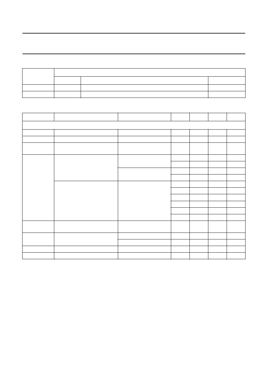
handbook, full pagewidth
LSB-JUSTIFIED FORMAT 16 BITS
LSB-JUSTIFIED FORMAT 18 BITS
LSB-JUSTIFIED FORMAT 20 BITS
INPUT FORMAT I
2
S-BUS
WS
LEFT
LEFT
LEFT
LEFT
RIGHT
RIGHT
RIGHT
RIGHT
3
2
2
2
15
16
17
18
1
15
16
1
1
3
2
1
MSB
B2
MSB
LSB
LSB
MSB
B2
MSB
LSB
B2
MSB
B2
B3
B4
B15
LSB
B17
2
15
16
17
18
1
MSB
B2
B3
B4
LSB
B17
2
15
16
17
18
19
20
1
MSB
B2
B3
B4
B5
B6
LSB
B19
MGD019
2
15
16
17
18
19
20
1
MSB
B2
B3
B4
B5
B6
LSB
B19
2
15
16
1
MSB
LSB
B2
B15
>=8
>=8
BCK
DATA
WS
BCK
DATA
WS
BCK
DATA
WS
BCK
DATA
Fig.3 Input formats.
1996 Jul 17
14
Philips Semiconductors
Objective specification
Bitstream continuous calibration filter-DAC
for CD-ROM audio applications
TDA1388
Fig.4 Timing address mode.
handbook, full pagewidth
t h;MA
t s;MA
t h;DAT
t s;DAT
Tcy
BIT 0
L3MODE
L3CLK
L3DATA
BIT 7
MGD016
tLC
tHC
t s;MA
t h;MA
Fig.5 Timing for data transfer mode.
handbook, full pagewidth
thalt
t s;MT
t EN;DAT
t h;DAT
t s;DAT
t h;DAT
t 3;DAT
thalt
t h;MT
MGD017
Tcy
BIT 0
L3MODE
L3CLK
L3DATA
write
BIT 7
tLC
tHC
1996 Jul 17
15
Philips Semiconductors
Objective specification
Bitstream continuous calibration filter-DAC
for CD-ROM audio applications
TDA1388
LIMITING VALUES
In accordance with the Absolute Maximum Rating System (IEC 134). All voltages referenced to ground,
V
DDD
= V
DDA
= V
DDO
= 5 V; T
amb
= 25
∞
C, unless otherwise specified.
Notes
1. All V
DD
and V
SS
connections must be made to the same power supply.
2. Equivalent to discharging a 100 pF capacitor via a 1.5 k
series resistor.
3. Equivalent to discharging a 200 pF capacitor via a 2.5
µ
H series inductor.
SYMBOL
PARAMETER
CONDITIONS
MIN.
MAX.
UNIT
V
DD
supply voltage
note 1
-
7.0
V
T
xtal(max)
maximum crystal temperature
-
150
∞
C
T
stg
storage temperature
-
65
+125
∞
C
T
amb
operating ambient temperature
-
20
+70
∞
C
V
es
electrostatic handling
note 2
-
3000
+3000
V
note 3
-
300
+300
V
Fig.6 Multibyte transfer.
handbook, full pagewidth
thalt
address
L3DATA
L3CLK
L3MODE
address
data byte #1
data byte #2
MGD018

1996 Jul 17
16
Philips Semiconductors
Objective specification
Bitstream continuous calibration filter-DAC
for CD-ROM audio applications
TDA1388
THERMAL CHARACTERISTICS
DC CHARACTERISTICS
V
DDD
= V
DDA
= V
DDO
= 5 V; T
amb
= 25
∞
C; R
L
= 5 k
; all voltages referenced to ground (pins 1, 13, 21 and 23);
unless otherwise specified
.
Notes
1. All power supply pins (V
DD
and V
SS
) must be connected to the same external power supply unit.
2. No operational amplifier load resistor.
3. Load capacitance larger than 50 pF, a 22
µ
H inductor in parallel with a 270
resistor must be inserted between the
load and the operational amplifier output (line output only).
SYMBOL
PARAMETER
VALUE
UNIT
R
th j-a
thermal resistance from junction to ambient in free air
SOP28
60
K/W
SSOP28
80
K/W
SYMBOL
PARAMETER
CONDITIONS
MIN.
TYP.
MAX.
UNIT
V
DDD
digital supply voltage
note 1
4.5
5.0
5.5
V
V
DDA
analog supply voltage
note 1
4.5
5.0
5.5
V
V
DDO
operational amplifier supply
voltage
note 1
4.5
5.0
5.5
V
I
DDD
digital supply current
at digital silence
-
7.0
-
mA
I
DDA
analog supply current
at digital silence
-
5.0
-
mA
I
DDO
operational amplifier supply
current
at digital silence
-
10
-
mA
P
tot
total power dissipation
note 2
-
110
-
mW
Digital input pins
V
IH
HIGH level input voltage
0.7V
DDD
-
V
DDD
+ 0.5 V
V
IL
LOW level input voltage
-
-
0.3V
DDD
V
|
I
LI
|
input leakage current
-
-
10
µ
A
C
in
input capacitance
-
-
10
pF
Analog audio pins
V
ref
reference voltage
with respect to V
SSA
0.45V
DDA
0.5V
DDA
0.55V
DDA
V
R
out(ref)
output reference resistance
-
3
-
k
R
CONV
current-to-voltage
conversion resistor
-
2.7
-
k
I
o(max)
maximum output current
(THD+N)/S < 0.1%
R
L
= 32
-
88
-
mA
(THD+N)/S < 0.1%
R
L
= 16
-
44
-
mA
C
L
output load capacitance
note 3
-
-
50
pF

1996 Jul 17
17
Philips Semiconductors
Objective specification
Bitstream continuous calibration filter-DAC
for CD-ROM audio applications
TDA1388
AC CHARACTERISTICS (ANALOG)
V
DDD
= V
DDA
= V
DDO
= 5 V; f
i
= 1 kHz; T
amb
= 25
∞
C; R
L
= 5 k
all voltages referenced to ground
(pins 1, 13, 21 and 23); unless otherwise specified
.
Notes
1. Proportional to V
DDA
.
2. One output digital silence, the other maximum volume.
SYMBOL
PARAMETER
CONDITIONS
MIN.
TYP.
MAX.
UNIT
RES
resolution
-
-
18
bits
V
FS(rms)
output voltage swing
(RMS value)
note 1
0.9
1.0
1.1
V
V
DC(os)
output voltage DC offset with
respect to reference voltage
level V
ref
-
20
-
mV
SVRR
supply voltage ripple rejection
V
DDA
and V
DDO
f
ripple
= 1 kHz;
V
ripple(p-p)
= 100 mV;
C
pin
= 10
µ
F
-
40
-
dB
V
o
unbalance between the 2 DAC
voltage outputs
maximum volume
-
0.1
-
dB
ct
crosstalk between the 2 DAC
voltage outputs for line outputs
R
L
= 5 k
, note 2
-
90
-
dB
crosstalk between the 2 DAC
voltage outputs for headphone
outputs
R
L
= 16
, note 2
-
60
-
dB
R
L
= 32
, note 2
-
65
-
dB
(THD+N)/S
total harmonic distortion plus
noise as a function of signal for
the line output
0 dB signal;
R
L
= 5 k
-
-
85
-
80
dB
-
0.006
0.013
%
-
60 dB signal;
R
L
= 5 k
-
-
35
-
30
dBA
-
1.8
3.2
%
total harmonic distortion plus
noise as a function of signal for
the headphone output
0 dB signal;
R
L
= 16
-
-
65
-
dB
-
0.056
-
%
0 dB signal;
R
L
= 32
-
-
70
-
dB
-
0.032
-
%
-
60 dB signal;
R
L
= 16
or R
L
= 32
-
-
35
-
30
dBA
-
1.8
3.2
%
S/N
signal-to-noise ratio at bipolar
zero
A weighting;
at code 00000H
90
95
-
dBA
1996 Jul 17
18
Philips Semiconductors
Objective specification
Bitstream continuous calibration filter-DAC
for CD-ROM audio applications
TDA1388
AC CHARACTERISTICS (DIGITAL)
V
DDD
= V
DDA
= V
DDO
= 4.5 to 5.5 V; T
amb
=
-
20 to +70
∞
C; R
L
= 5 k
; all voltages referenced to ground
(pins 1, 13, 21 and 23); unless otherwise specified
.
SYMBOL
PARAMETER
CONDITIONS
MIN.
TYP.
MAX
UNIT
T
cy
clock cycle
f
sys
= 256f
s
81.3
88.6
122
ns
f
sys
= 384f
s
54.2
59.1
81.3
ns
t
CWL
f
sys
LOW level pulse width
22
-
-
ns
t
CWH
f
sys
HIGH level pulse width
22
-
-
ns
Serial input data timing (see Fig.7)
BR
clock input = data input rate
f
sys
= 256f
s
-
64f
s
-
f
sys
= 384f
s
-
48f
s
-
f
sys
system clock frequency
8.192
-
18.432
MHz
f
WS
word selection input frequency
-
44.1
48
kHz
t
r
rise time
-
-
20
ns
t
f
fall time
-
-
20
ns
t
BCK(H)
bit clock HIGH time
55
-
-
ns
t
BCK(L)
bit clock LOW time
55
-
-
ns
t
s;DAT
data set-up time
10
-
-
ns
t
h;DAT
data hold time
20
-
-
ns
t
s;WS
word selection set-up time
20
-
-
ns
t
h;WS
word selection hold time
10
-
-
ns
Fig.7 Timing and input signals.
handbook, full pagewidth
MGD567
WS
BCK
DATA
RIGHT
LSB
MSB
LEFT
ts;WS
th;WS
ts;DAT
th;DAT
tBCK(H)
tBCK(L)
Tcy
tr
tr
1996 Jul 17
19
Philips Semiconductors
Objective specification
Bitstream continuous calibration filter-DAC
for CD-ROM audio applications
TDA1388
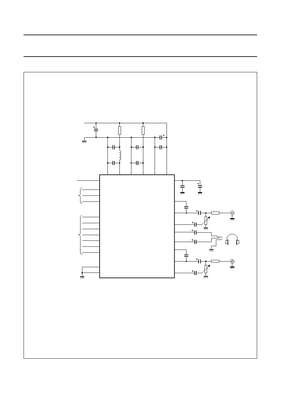
TEST AND APPLICATION INFORMATION
Fig.8 Application diagram.
(1) Optional.
(2) Chip inductor BLM32A07.
handbook, full pagewidth
Vref
APPL0/DA
APPL1/MO
TC
ACP
APPL2/CL
DATA
WS
BCK
19
14
SYSCLK
SYSSEL
15
7
IF1
IF2
8
13
VSSD VDDD
12
5
TDA1388
4
23
18
11
10
9
16
17
22
3
28
1
6
2
27
24
R
L
25
26
VSSO1
VSSA
VDDO
VDDA
100
100
µ
F
10
µ
F
100 nF
100 nF
330
µ
F
100 nF
100 nF
100 nF
FILTCL
HPINL
HPOUTR
HPOUTL
VOL
1
nF
100
µ
F
4.7
4.7
+
5 V
I
2
S-BUS OR
LSB-JUSTIFIED
SERIAL INPUT DATA
SYSTEM
CLOCK
INPUT
L3
(1)
(2)
(1)
from
MICROCONTROLLER
20
21
47
µ
F
4.7
µ
F
330
µ
F
330
µ
F
R1
10 k
MGD152
100
FILTCR
HPINR
VOR
VSSO2
1
nF 47
µ
F
4.7
µ
F
R1
10 k

1996 Jul 17
20
Philips Semiconductors
Objective specification
Bitstream continuous calibration filter-DAC
for CD-ROM audio applications
TDA1388
PACKAGE OUTLINES
UNIT
A
max.
A
1
A
2
A
3
b
p
c
D
(1)
E
(1)
(1)
e
H
E
L
L
p
Q
Z
y
w
v
REFERENCES
OUTLINE
VERSION
EUROPEAN
PROJECTION
ISSUE DATE
IEC
JEDEC
EIAJ
mm
inches
2.65
0.30
0.10
2.45
2.25
0.49
0.36
0.32
0.23
18.1
17.7
7.6
7.4
1.27
10.65
10.00
1.1
1.0
0.9
0.4
8
0
o
o
0.25
0.1
DIMENSIONS (inch dimensions are derived from the original mm dimensions)
Note
1. Plastic or metal protrusions of 0.15 mm maximum per side are not included.
1.1
0.4
SOT136-1
91-08-13
95-01-24
X
14
28
w
M
A
A
1
A
2
b
p
D
H
E
L
p
Q
detail X
E
Z
c
L
v
M
A
e
15
1
(A )
3
A
y
0.25
075E06
MS-013AE
pin 1 index
0.10
0.012
0.004
0.096
0.089
0.019
0.014
0.013
0.009
0.71
0.69
0.30
0.29
0.050
1.4
0.055
0.42
0.39
0.043
0.039
0.035
0.016
0.01
0.25
0.01
0.004
0.043
0.016
0.01
0
5
10 mm
scale
SO28: plastic small outline package; 28 leads; body width 7.5 mm
SOT136-1

1996 Jul 17
21
Philips Semiconductors
Objective specification
Bitstream continuous calibration filter-DAC
for CD-ROM audio applications
TDA1388
UNIT
A
1
A
2
A
3
b
p
c
D
(1)
E
(1)
(1)
e
H
E
L
L
p
Q
Z
y
w
v
REFERENCES
OUTLINE
VERSION
EUROPEAN
PROJECTION
ISSUE DATE
IEC
JEDEC
EIAJ
mm
0.21
0.05
1.80
1.65
0.38
0.25
0.20
0.09
10.4
10.0
5.4
5.2
0.65
1.25
7.9
7.6
0.9
0.7
1.1
0.7
8
0
o
o
0.13
0.1
0.2
DIMENSIONS (mm are the original dimensions)
Note
1. Plastic or metal protrusions of 0.20 mm maximum per side are not included.
1.03
0.63
SOT341-1
MO-150AH
93-09-08
95-02-04
X
w
M
A
A
1
A
2
b
p
D
H
E
L
p
Q
detail X
E
Z
e
c
L
v
M
A
(A )
3
A
1
14
28
15
0.25
y
pin 1 index
0
2.5
5 mm
scale
SSOP28: plastic shrink small outline package; 28 leads; body width 5.3 mm
SOT341-1
A
max.
2.0

1996 Jul 17
22
Philips Semiconductors
Objective specification
Bitstream continuous calibration filter-DAC
for CD-ROM audio applications
TDA1388
SOLDERING
Introduction
There is no soldering method that is ideal for all IC
packages. Wave soldering is often preferred when
through-hole and surface mounted components are mixed
on one printed-circuit board. However, wave soldering is
not always suitable for surface mounted ICs, or for
printed-circuits with high population densities. In these
situations reflow soldering is often used.
This text gives a very brief insight to a complex technology.
A more in-depth account of soldering ICs can be found in
our
"IC Package Databook" (order code 9398 652 90011).
Reflow soldering
Reflow soldering techniques are suitable for all SO and
SSOP packages.
Reflow soldering requires solder paste (a suspension of
fine solder particles, flux and binding agent) to be applied
to the printed-circuit board by screen printing, stencilling or
pressure-syringe dispensing before package placement.
Several techniques exist for reflowing; for example,
thermal conduction by heated belt. Dwell times vary
between 50 and 300 seconds depending on heating
method. Typical reflow temperatures range from
215 to 250
∞
C.
Preheating is necessary to dry the paste and evaporate
the binding agent. Preheating duration: 45 minutes at
45
∞
C.
Wave soldering
SO
Wave soldering techniques can be used for all SO
packages if the following conditions are observed:
∑
A double-wave (a turbulent wave with high upward
pressure followed by a smooth laminar wave) soldering
technique should be used.
∑
The longitudinal axis of the package footprint must be
parallel to the solder flow.
∑
The package footprint must incorporate solder thieves at
the downstream end.
SSOP
Wave soldering is not recommended for SSOP packages.
This is because of the likelihood of solder bridging due to
closely-spaced leads and the possibility of incomplete
solder penetration in multi-lead devices.
If wave soldering cannot be avoided, the following
conditions must be observed:
∑
A double-wave (a turbulent wave with high upward
pressure followed by a smooth laminar wave)
soldering technique should be used.
∑
The longitudinal axis of the package footprint must
be parallel to the solder flow and must incorporate
solder thieves at the downstream end.
Even with these conditions, only consider wave
soldering SSOP packages that have a body width of
4.4 mm, that is SSOP16 (SOT369-1) or
SSOP20 (SOT266-1).
M
ETHOD
(SO
AND
SSOP)
During placement and before soldering, the package must
be fixed with a droplet of adhesive. The adhesive can be
applied by screen printing, pin transfer or syringe
dispensing. The package can be soldered after the
adhesive is cured.
Maximum permissible solder temperature is 260
∞
C, and
maximum duration of package immersion in solder is
10 seconds, if cooled to less than 150
∞
C within
6 seconds. Typical dwell time is 4 seconds at 250
∞
C.
A mildly-activated flux will eliminate the need for removal
of corrosive residues in most applications.
Repairing soldered joints
Fix the component by first soldering two diagonally-
opposite end leads. Use only a low voltage soldering iron
(less than 24 V) applied to the flat part of the lead. Contact
time must be limited to 10 seconds at up to 300
∞
C. When
using a dedicated tool, all other leads can be soldered in
one operation within 2 to 5 seconds between
270 and 320
∞
C.

1996 Jul 17
23
Philips Semiconductors
Objective specification
Bitstream continuous calibration filter-DAC
for CD-ROM audio applications
TDA1388
DEFINITIONS
LIFE SUPPORT APPLICATIONS
These products are not designed for use in life support appliances, devices, or systems where malfunction of these
products can reasonably be expected to result in personal injury. Philips customers using or selling these products for
use in such applications do so at their own risk and agree to fully indemnify Philips for any damages resulting from such
improper use or sale.
Data sheet status
Objective specification
This data sheet contains target or goal specifications for product development.
Preliminary specification
This data sheet contains preliminary data; supplementary data may be published later.
Product specification
This data sheet contains final product specifications.
Limiting values
Limiting values given are in accordance with the Absolute Maximum Rating System (IEC 134). Stress above one or
more of the limiting values may cause permanent damage to the device. These are stress ratings only and operation
of the device at these or at any other conditions above those given in the Characteristics sections of the specification
is not implied. Exposure to limiting values for extended periods may affect device reliability.
Application information
Where application information is given, it is advisory and does not form part of the specification.

Internet: http://www.semiconductors.philips.com/ps/
(1)
TDA1388_2 June 26, 1996 11:51 am
Philips Semiconductors ≠ a worldwide company
© Philips Electronics N.V. 1996
SCA50
All rights are reserved. Reproduction in whole or in part is prohibited without the prior written consent of the copyright owner.
The information presented in this document does not form part of any quotation or contract, is believed to be accurate and reliable and may be changed
without notice. No liability will be accepted by the publisher for any consequence of its use. Publication thereof does not convey nor imply any license
under patent- or other industrial or intellectual property rights.
Netherlands: Postbus 90050, 5600 PB EINDHOVEN, Bldg. VB,
Tel. +31 40 27 83749, Fax. +31 40 27 88399
New Zealand: 2 Wagener Place, C.P.O. Box 1041, AUCKLAND,
Tel. +64 9 849 4160, Fax. +64 9 849 7811
Norway: Box 1, Manglerud 0612, OSLO,
Tel. +47 22 74 8000, Fax. +47 22 74 8341
Philippines: Philips Semiconductors Philippines Inc.,
106 Valero St. Salcedo Village, P.O. Box 2108 MCC, MAKATI,
Metro MANILA, Tel. +63 2 816 6380, Fax. +63 2 817 3474
Poland: Ul. Lukiska 10, PL 04-123 WARSZAWA,
Tel. +48 22 612 2831, Fax. +48 22 612 2327
Portugal: see Spain
Romania: see Italy
Russia: Philips Russia, Ul. Usatcheva 35A, 119048 MOSCOW,
Tel. +7 095 926 5361, Fax. +7 095 564 8323
Singapore: Lorong 1, Toa Payoh, SINGAPORE 1231,
Tel. +65 350 2538, Fax. +65 251 6500
Slovakia: see Austria
Slovenia: see Italy
South Africa: S.A. PHILIPS Pty Ltd., 195-215 Main Road Martindale,
2092 JOHANNESBURG, P.O. Box 7430 Johannesburg 2000,
Tel. +27 11 470 5911, Fax. +27 11 470 5494
South America: Rua do Rocio 220, 5th floor, Suite 51,
04552-903 S„o Paulo, S√O PAULO - SP, Brazil,
Tel. +55 11 821 2333, Fax. +55 11 829 1849
Spain: Balmes 22, 08007 BARCELONA,
Tel. +34 3 301 6312, Fax. +34 3 301 4107
Sweden: Kottbygatan 7, Akalla, S-16485 STOCKHOLM,
Tel. +46 8 632 2000, Fax. +46 8 632 2745
Switzerland: Allmendstrasse 140, CH-8027 ZÐRICH,
Tel. +41 1 488 2686, Fax. +41 1 481 7730
Taiwan: PHILIPS TAIWAN Ltd., 23-30F, 66,
Chung Hsiao West Road, Sec. 1, P.O. Box 22978,
TAIPEI 100, Tel. +886 2 382 4443, Fax. +886 2 382 4444
Thailand: PHILIPS ELECTRONICS (THAILAND) Ltd.,
209/2 Sanpavuth-Bangna Road Prakanong, BANGKOK 10260,
Tel. +66 2 745 4090, Fax. +66 2 398 0793
Turkey: Talatpasa Cad. No. 5, 80640 GÐLTEPE/ISTANBUL,
Tel. +90 212 279 2770, Fax. +90 212 282 6707
Ukraine: PHILIPS UKRAINE, 2A Akademika Koroleva str., Office 165,
252148 KIEV, Tel. +380 44 476 0297/1642, Fax. +380 44 476 6991
United Kingdom: Philips Semiconductors Ltd., 276 Bath Road, Hayes,
MIDDLESEX UB3 5BX, Tel. +44 181 730 5000, Fax. +44 181 754 8421
United States: 811 East Arques Avenue, SUNNYVALE, CA 94088-3409,
Tel. +1 800 234 7381, Fax. +1 708 296 8556
Uruguay: see South America
Vietnam: see Singapore
Yugoslavia: PHILIPS, Trg N. Pasica 5/v, 11000 BEOGRAD,
Tel. +381 11 825 344, Fax.+381 11 635 777
For all other countries apply to: Philips Semiconductors, Marketing & Sales Communications,
Building BE-p, P.O. Box 218, 5600 MD EINDHOVEN, The Netherlands, Fax. +31 40 27 24825
Argentina: see South America
Australia: 34 Waterloo Road, NORTH RYDE, NSW 2113,
Tel. +61 2 9805 4455, Fax. +61 2 9805 4466
Austria: Computerstr. 6, A-1101 WIEN, P.O. Box 213,
Tel. +43 1 60 101, Fax. +43 1 60 101 1210
Belarus: Hotel Minsk Business Center, Bld. 3, r. 1211, Volodarski Str. 6,
220050 MINSK, Tel. +375 172 200 733, Fax. +375 172 200 773
Belgium: see The Netherlands
Brazil: see South America
Bulgaria: Philips Bulgaria Ltd., Energoproject, 15th floor,
51 James Bourchier Blvd., 1407 SOFIA,
Tel. +359 2 689 211, Fax. +359 2 689 102
Canada: PHILIPS SEMICONDUCTORS/COMPONENTS,
Tel. +1 800 234 7381, Fax. +1 708 296 8556
China/Hong Kong: 501 Hong Kong Industrial Technology Centre,
72 Tat Chee Avenue, Kowloon Tong, HONG KONG,
Tel. +852 2319 7888, Fax. +852 2319 7700
Colombia: see South America
Czech Republic: see Austria
Denmark: Prags Boulevard 80, PB 1919, DK-2300 COPENHAGEN S,
Tel. +45 32 88 2636, Fax. +45 31 57 1949
Finland: Sinikalliontie 3, FIN-02630 ESPOO,
Tel. +358 615 800, Fax. +358 615 80920
France: 4 Rue du Port-aux-Vins, BP317, 92156 SURESNES Cedex,
Tel. +33 1 40 99 6161, Fax. +33 1 40 99 6427
Germany: Hammerbrookstraþe 69, D-20097 HAMBURG,
Tel. +49 40 23 52 60, Fax. +49 40 23 536 300
Greece: No. 15, 25th March Street, GR 17778 TAVROS,
Tel. +30 1 4894 339/911, Fax. +30 1 4814 240
Hungary: see Austria
India: Philips INDIA Ltd, Shivsagar Estate, A Block, Dr. Annie Besant Rd.
Worli, MUMBAI 400 018, Tel. +91 22 4938 541, Fax. +91 22 4938 722
Indonesia: see Singapore
Ireland: Newstead, Clonskeagh, DUBLIN 14,
Tel. +353 1 7640 000, Fax. +353 1 7640 200
Israel: RAPAC Electronics, 7 Kehilat Saloniki St, TEL AVIV 61180,
Tel. +972 3 645 0444, Fax. +972 3 648 1007
Italy: PHILIPS SEMICONDUCTORS, Piazza IV Novembre 3,
20124 MILANO, Tel. +39 2 6752 2531, Fax. +39 2 6752 2557
Japan: Philips Bldg 13-37, Kohnan 2-chome, Minato-ku, TOKYO 108,
Tel. +81 3 3740 5130, Fax. +81 3 3740 5077
Korea: Philips House, 260-199 Itaewon-dong, Yongsan-ku, SEOUL,
Tel. +82 2 709 1412, Fax. +82 2 709 1415
Malaysia: No. 76 Jalan Universiti, 46200 PETALING JAYA, SELANGOR,
Tel. +60 3 750 5214, Fax. +60 3 757 4880
Mexico: 5900 Gateway East, Suite 200, EL PASO, TEXAS 79905,
Tel. +1 800 234 7381, Fax. +1 708 296 8556
Middle East: see Italy
Printed in The Netherlands
517021/50/02/pp24
Date of release: 1996 Jul 17
Document order number:
9397 750 00965