
DATA SHEET
Product specification
File under Integrated Circuits, IC01
February 1991
INTEGRATED CIRCUITS
TDA1541A
Stereo high performance 16-bit
DAC

February 1991
2
Philips Semiconductors
Product specification
Stereo high performance 16-bit DAC
TDA1541A
FEATURES
∑
High sound quality
∑
High performance: low noise and distortion, wide
dynamic range
∑
4
◊
or 8
◊
oversampling possible
∑
Selectable two-channel input format
∑
TTL compatible inputs.
GENERAL DESCRIPTION
The TDA1541A is a stereo 16-bit digital-to-analog
converter (DAC). The ingenious design of the electronic
circuit guarantees a high performance and superior sound
quality. The TDA1541A is therefore extremely suitable for
use in top-end hi-fi digital audio equipment such as high
quality Compact Disc players or digital amplifiers.
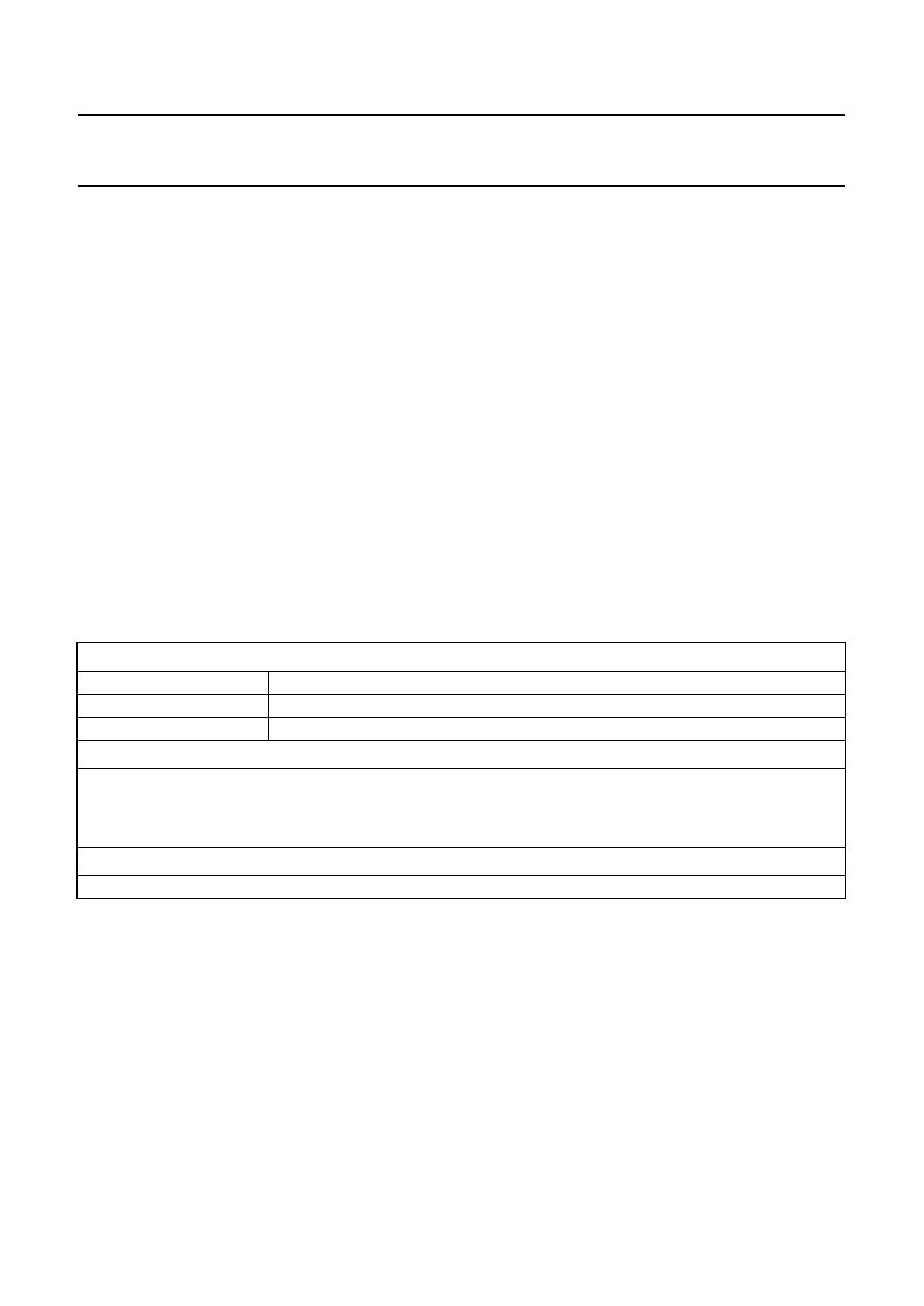
ORDERING INFORMATION
Note
1. SOT117; SOT117-1; 1996 August 09.
QUICK REFERENCE DATA
EXTENDED TYPE
NUMBER
PACKAGE
PINS
PIN POSITION
MATERIAL
CODE
TDA1541A
(1)
28
DIL
plastic
SOT117
SYMBOL
PARAMETER
CONDITIONS
MIN.
TYP.
MAX.
UNIT
V
DD
supply voltage; pin 28
4.5
5.0
5.5
V
-
V
DD1
supply voltage; pin 26
4.5
5.0
5.5
V
-
V
DD2
supply voltage; pin 15
14.0
15.0
16.0
V
I
DD
supply current; pin 28
-
27
40
mA
-
I
DD1
supply current; pin 26
-
37
50
mA
-
I
DD2
supply current; pin 15
-
25
35
mA
THD
total harmonic distortion
including noise
-
-
95
-
90
dB
at 0 dB
-
0.0018
0.0032
%
THD
total harmonic distortion
including noise
-
-
42
-
dB
at
-
60 dB
-
0.79
-
%
NL
non-linearity
at T
amb
=
-
20 to
+
85
∞
C
-
0.5
1.0
LSB
t
cs
current settling time to
±
1LSB
-
0.5
-
µ
s
BR
input bit rate at data input;
(pin 3 and 4)
-
-
6.4
Mbits/s
f
BCK
clock frequency at clock input
-
-
6.4
MHz
TC
FS
full scale temperature coefficient
at analog
(AOL;AOR)
-
±
200
◊
10
-6
-
K
-1
T
amb
operating ambient temperature range
-
40
-
+85
∞
C
P
tot
total power dissipation
-
700
-
mW

February 1991
3
Philips Semiconductors
Product specification
Stereo high performance 16-bit DAC
TDA1541A
Fig.1 Block diagram.
(1) TDA1542.
(2) 2
◊
NE5534 or equivalent.
February 1991
4
Philips Semiconductors
Product specification
Stereo high performance 16-bit DAC
TDA1541A
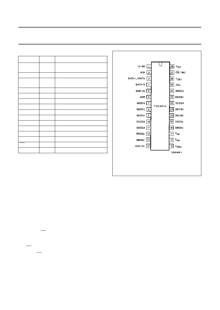
PINNING
Note
1. See Table 1 data selection input.
SYMBOL
PIN
DESCRIPTION
LE/WS
(1)
1
latch enable input/ word select
input
BCK
(1)
2
bit clock input
DATA L
/DATA
(1)
3
data left channel input/ data
input (selected format)
DATA R
(1)
4
data right channel input
GND(A)
5
analog ground
AOR
6
right channel output
DECOU
7 to 13
decoupling
GND (D)
14
digital ground
V
DD2
15
-
15 V supply voltage
COSC
16,17
oscillator
DECOU
18 to 24 decoupling
AOL
25
left channel output
V
DD1
26
-
5 V supply voltage
OB/TWC
(1)
27
mode select input
V
DD
28
+5 V supply voltage
Fig.2 Pin configuration
FUNCTIONAL DESCRIPTION
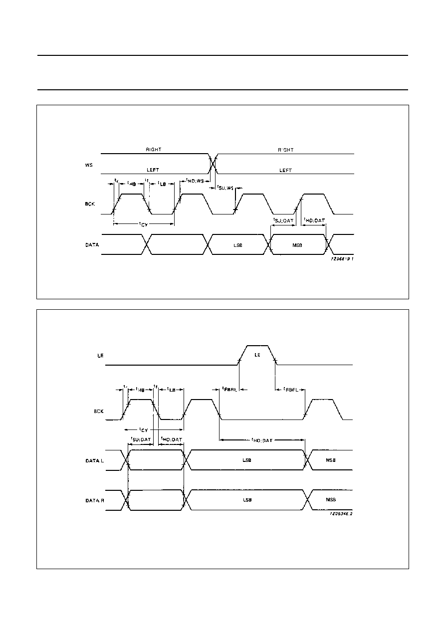
The TDA1541A accepts input sample formats in time multiplexed mode or simultaneous mode up to 16-bit word length.
The most significant bit (MSB) must always be first. The flexible input data format allows easy interfacing with signal
processing chips such as interpolation filters, error correction circuits, pulse code modulation adaptors and audio signal
processors (ASP).
The high maximum input bit-rate and fast setting facilitates application in 8
◊
oversampling systems
(44.1 kHz to 352.8 kHz or 48 kHz to 384 kHz) with the associated simple analog filtering function (low order, linear phase
filter).
Input data selection (see also Table 1)
With the input OB/TWC connected to ground, data input (offset binary format) must be in time multiplexed mode. It is
accompanied with a word select (WS) and a bit clock input (BCK) signal. The converted samples appear at the output,
at the first positive going transition of the bit clock signal after a negative going transition of the word select signal.
With OB/TWC connected to V
DD
the mode is the same but the data format must be in the two's complement.
When input OB/TWC input is connected to V
DD1
the two channels of data (L/R) are input simultaneously via DATA L and
DATA R, accompanied with BCK and a latch-enable input (LE). With this mode selected the data must be in offset binary.
The converted samples appear at the output at the positive going transition of the latch enable signal.
The format of the data input signals is shown in Fig.5 and 6.

February 1991
5
Philips Semiconductors
Product specification
Stereo high performance 16-bit DAC
TDA1541A
True 16-bit performance is achieved by each channel using three 2-bit active dividers, operating on the dynamic element
matching principle, in combination with a 10-bit passive current divider, based on emitter scaling. All digital inputs are
TTL compatible.
Table 1
Input data selection
Where:
LIMITING VALUES
In accordance with the Absolute Maximum System (IEC 134)
* Equivalent to discharging a 100 pF capacitor through a 1.5 k
series resistor.
THERMAL RESISTANCE
OB/TWC
MODE
PIN 1
PIN 2
PIN 3
PIN 4
-
5 V
simultaneous
LE
BCK
DATA L
DATA R
0 V
time MUX OB
WS
BCK
DATA OB
not used
+5 V
time MUX TWC
WS
BCK
DATA TWC
not used
LE
= latch enable
WS
= word select,
LOW = left channel;
HIGH = right channel
BCK
= bit clock
DATA L
= data left
DATA R
= data right
DATA OB
= data offset binary
DATA TWC
= data two's complement
MUX OB
= mulitplexed offset binary
MUX TWC
= multiplexed two's
complement = I
2
S- format
SYMBOL
PARAMETER
CONDITIONS
MIN.
MAX.
UNIT
V
DD
supply voltage; pin 28
0
7
V
-
V
DD1
supply voltage; pin 26
0
7
V
-
V
DD2
supply voltage; pin 15
0
17
V
T
stg
storage temperature range
-
55
+150
∞
C
T
amb
operating ambient temperature range
-
40
+85
∞
C
V
es
electrostatic handling*
-
1000
+1000
V
SYMBOL
PARAMETER
TYP.
UNIT
R
th j-a
from junction to ambient
30
K/W

February 1991
6
Philips Semiconductors
Product specification
Stereo high performance 16-bit DAC
TDA1541A
CHARACTERISTICS
V
DD
= 5 V;
-
V
DD1
= 5 V;
-
V
DD2
= 15 V; T
amb
= +25
∞
C; mea sured in the circuit of Fig.1; unless otherwise specified
SYMBOL
PARAMETER
CONDITIONS
MIN.
TYP.
MAX.
UNIT
Supply
V
DD
supply voltage; pin 28
4.5
5.0
5.5
V
-
V
DD1
supply voltage; pin 26
4.5
5.0
5.5
V
-
V
DD2
supply voltage; pin 15
14.0
15.0
16.0
V
V
GND(A)
-
V
GND(D)
voltage difference between
analog and digital ground
-
0.3
0
+0.3
V
I
DD
supply current; pin 28
-
27
40
mA
-
I
DD1
supply current; pin 26
-
37
50
mA
-
I
DD2
supply current; pin 15
-
25
35
mA
Inputs
input current pins (1, 2, 3 and 4)
-
I
IL
digital inputs LOW
V
I
= 0.8 V
-
-
0.4
mA
I
IH
digital inputs HIGH
V
I
= 2.0 V
-
-
20
µ
A
Digital input currents (pin 27)
I
OB/TWC
+5 V
-
-
1
µ
A
I
OB/TWC
0 V
-
-
20
µ
A
I
OB/TWC
-
5 V
-
-
40
µ
A
input frequency/bit rate
f
BCK
clock input pin 2
-
-
6.4
MHz
BR
bit rate data input pin 3 and 4
-
-
6.4
Mbits/s
f
WS
word select input pin 2
-
-
200
kHz
f
LE
latch enable input 1
-
-
200
kHz
C
I
input capacitance of digital inputs
-
12
-
pF
Analog outputs (AOL;AOR; see note 1)
Res
resolution
-
16
-
bits
I
FS
full scale current
3.4
4.0
4.6
mA
I
ZS
zero scale current
-
25
50
nA
T
CFS
full scale temperature coefficient
T
amb
=
-
20 to +85
∞
C
-
±
200
◊
10
-
6
-
K
-
1
Analog outputs (V
ref
)
E
L
integral linearity error
T
amb
= 25
∞
C
-
0.5
1.0
LSB
E
L
integral linearity error
T
amb
=
-
20 to +85
∞
C
-
-
1.0
LSB
E
dL
differential linearity error
T
amb
= 20
∞
C,
note 2
-
0.5
1.0
LSB
E
dL
differential linearity error
T
amb
=
-
20 to
+
85
∞
C
-
-
1.0
LSB
THD
total harmonic distortion
at 0 dB; note 3
-
100
-
-
dB
-
0.0010
-
%

February 1991
7
Philips Semiconductors
Product specification
Stereo high performance 16-bit DAC
TDA1541A
Notes to the characteristics
1. To ensure no performance losses, permitted output voltage compliance is
±
25 mV maximum.
2. Selections have been made with respect to the maximum differential linearity error (E
dL
):
TDA1541A/N2
bit 1-16
E
dL
< 1 LSB
TDA1541A/N2/R1
bit 1-16
E
dL
< 2 LSB
TDA1541A/N2/S1
bit 1-7
E
dL
< 0.5 LSB
bit 8-15
E
dL
< 1 LSB
bit 16
E
dL
< 0.75 LSB
THD
total harmonic distortion
including noise
at 0 dB;
note 3, Fig. 3, 4
-
-
-
95
0.0018
-
90
0.0032
dB
%
THD
total harmonic distortion
including noise
at
-
60 dB;
note 3, Fig. 3, 4
-
-
-
42
0.79
-
-
dB
%
t
cs
settling time
±
1 LSB
-
0.5
-
µ
s
channel separation
90
98
-
dB
|d
IO
|
unbalance between outputs
note 4
-
< 0.1
0.3
dB
|t
d
|
time delay between outputs
-
-
0.2
µ
s
SSVR
supply voltage ripple rejection
V
DD
= +5 V;
note 4
-
-
76
-
dB
SSVR
supply voltage ripple rejection
V
DD1
=
-
5 V;
note 4
-
-
84
-
dB
SSVR
supply voltage ripple rejection
V
DD2
=
-
15 V;
note 4
-
-
58
-
dB
S/N
signal-to-noise ratio
at bipolar zero
-
110
-
dB
S/N
signal-to-noise ratio
at full scale
98
104
-
dB
Timing (Fig. 5 and 6)
t
r
rise time
-
-
32
ns
t
f
fall time
-
-
32
ns
t
CY
bit clock cycle time
156
-
-
ns
t
HB
bit clock HIGH time
46
-
-
ns
t
LB
bit clock LOW time
46
-
-
ns
t
FBRL
bit clock fall time to latch enable
rise time
0
-
-
ns
t
RBFL
bit clock rise time to latch enable
fall time
0
-
-
ns
t
SU;DAT
data set-up time
32
-
-
ns
t
HD;DAT
data hold time to bit clock
0
-
-
ns
t
HD;WS
word select hold time
0
-
-
ns
t
SU;WS
word select set-up time
32
-
-
ns
SYMBOL
PARAMETER
CONDITIONS
MIN.
TYP.
MAX.
UNIT
February 1991
8
Philips Semiconductors
Product specification
Stereo high performance 16-bit DAC
TDA1541A
The S1 version has been specially selected to achieve extremely good performance even for small signals.
3. Measured using a 1 kHz sinewave generated at a sampling rate of 176.4 kHz.
4. V
ripple
= 100 mV and f
ripple
= 100 Hz.
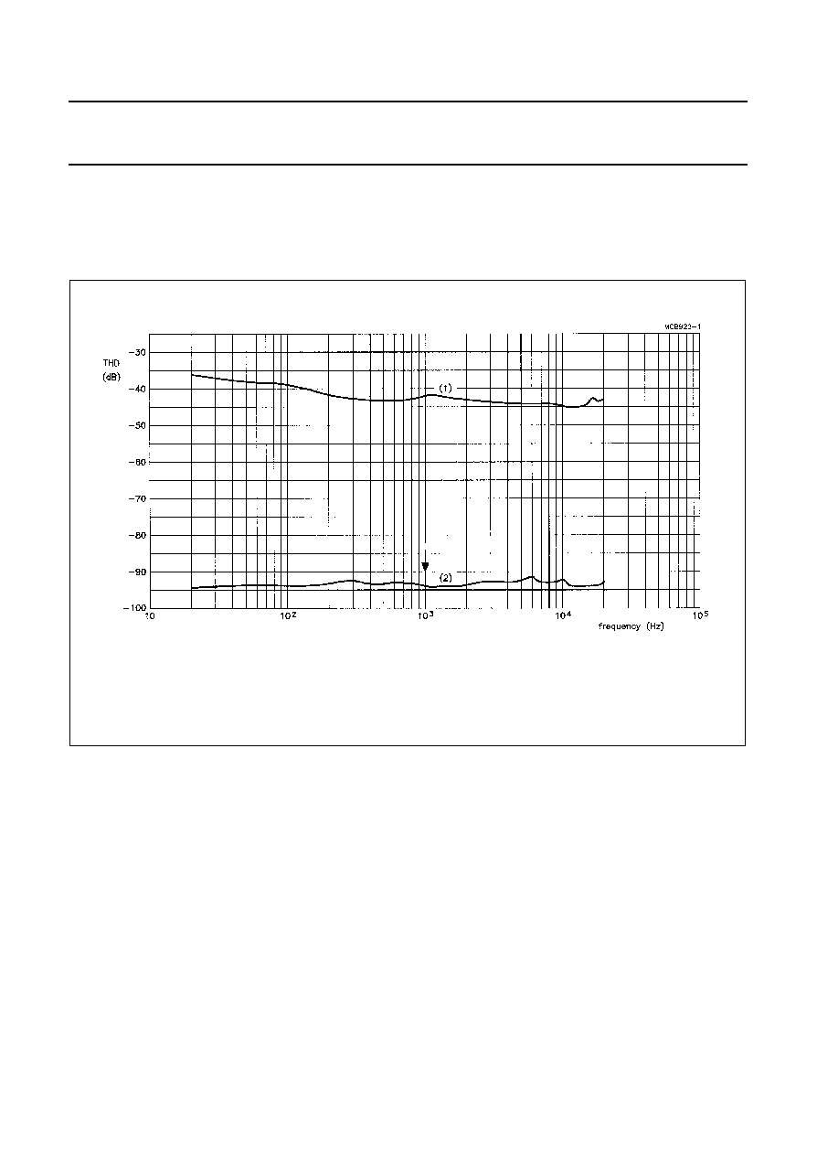
Notes to Fig.3
∑
The sample frequency 4FS: 176.4 kHz.
∑
Ref: 0 dB is the output level of a full scale digital sine wave stimulus.
(1) Measured including all distortion plus noise at a signal level of
-
60 dB.
(2) Measured including all distortion plus noise at a signal level of
-
0 dB.
Fig.3 Distortion as a function of frequency (4FS).
February 1991
9
Philips Semiconductors
Product specification
Stereo high performance 16-bit DAC
TDA1541A
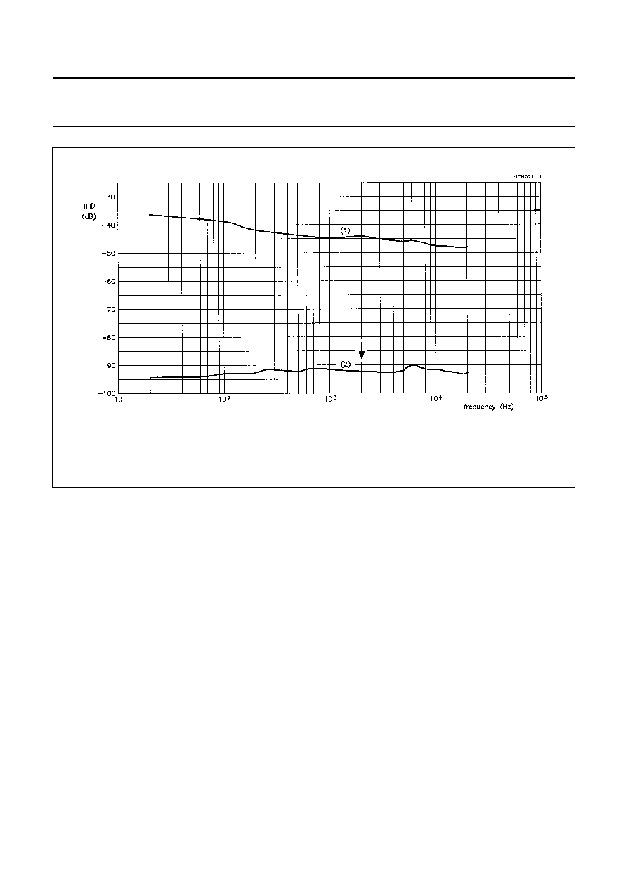
Notes to Fig.4
∑
The sample frequency 8FS: 352.8 kHz.
∑
Ref: 0 dB is the output level of a full scale digital sine wave stimulus.
Fig.4 Distortion as a function of frequency (8FS).
(1) Measured including all distortion plus noise at a signal level of
-
60 dB.
(2) Measured including all distortion plus noise at a signal level of
-
0 dB.
February 1991
10
Philips Semiconductors
Product specification
Stereo high performance 16-bit DAC
TDA1541A
Fig.5 Format of input signals; time multiplexed (I
2
S format).
Fig.6 Format of input signals; simultaneous data.

February 1991
11
Philips Semiconductors
Product specification
Stereo high performance 16-bit DAC
TDA1541A
PACKAGE OUTLINE
UNIT
A
max.
1
2
b
1
(1)
(1)
(1)
c
D
E
w
e
M
H
L
REFERENCES
OUTLINE
VERSION
EUROPEAN
PROJECTION
ISSUE DATE
IEC
JEDEC
EIAJ
mm
inches
DIMENSIONS (inch dimensions are derived from the original mm dimensions)
SOT117-1
92-11-17
95-01-14
A
min.
A
max.
b
Z
max.
M
E
e
1
1.7
1.3
0.53
0.38
0.32
0.23
36.0
35.0
14.1
13.7
3.9
3.4
0.25
2.54
15.24
15.80
15.24
17.15
15.90
1.7
5.1
0.51
4.0
0.066
0.051
0.020
0.014
0.013
0.009
1.41
1.34
0.56
0.54
0.15
0.13
0.01
0.10
0.60
0.62
0.60
0.68
0.63
0.067
0.20
0.020
0.16
051G05
MO-015AH
M
H
c
(e )
1
M
E
A
L
seating plane
A
1
w
M
b
1
e
D
A
2
Z
28
1
15
14
b
E
pin 1 index
0
5
10 mm
scale
Note
1. Plastic or metal protrusions of 0.25 mm maximum per side are not included.
handbook, full pagewidth
DIP28: plastic dual in-line package; 28 leads (600 mil)
SOT117-1
February 1991
12
Philips Semiconductors
Product specification
Stereo high performance 16-bit DAC
TDA1541A
SOLDERING
Introduction
There is no soldering method that is ideal for all IC
packages. Wave soldering is often preferred when
through-hole and surface mounted components are mixed
on one printed-circuit board. However, wave soldering is
not always suitable for surface mounted ICs, or for
printed-circuits with high population densities. In these
situations reflow soldering is often used.
This text gives a very brief insight to a complex technology.
A more in-depth account of soldering ICs can be found in
our
"IC Package Databook" (order code 9398 652 90011).
Soldering by dipping or by wave
The maximum permissible temperature of the solder is
260
∞
C; solder at this temperature must not be in contact
with the joint for more than 5 seconds. The total contact
time of successive solder waves must not exceed
5 seconds.
The device may be mounted up to the seating plane, but
the temperature of the plastic body must not exceed the
specified maximum storage temperature (T
stg max
). If the
printed-circuit board has been pre-heated, forced cooling
may be necessary immediately after soldering to keep the
temperature within the permissible limit.
Repairing soldered joints
Apply a low voltage soldering iron (less than 24 V) to the
lead(s) of the package, below the seating plane or not
more than 2 mm above it. If the temperature of the
soldering iron bit is less than 300
∞
C it may remain in
contact for up to 10 seconds. If the bit temperature is
between 300 and 400
∞
C, contact may be up to 5 seconds.
DEFINITIONS
LIFE SUPPORT APPLICATIONS
These products are not designed for use in life support appliances, devices, or systems where malfunction of these
products can reasonably be expected to result in personal injury. Philips customers using or selling these products for
use in such applications do so at their own risk and agree to fully indemnify Philips for any damages resulting from such
improper use or sale.
Data sheet status
Objective specification
This data sheet contains target or goal specifications for product development.
Preliminary specification
This data sheet contains preliminary data; supplementary data may be published later.
Product specification
This data sheet contains final product specifications.
Limiting values
Limiting values given are in accordance with the Absolute Maximum Rating System (IEC 134). Stress above one or
more of the limiting values may cause permanent damage to the device. These are stress ratings only and operation
of the device at these or at any other conditions above those given in the Characteristics sections of the specification
is not implied. Exposure to limiting values for extended periods may affect device reliability.
Application information
Where application information is given, it is advisory and does not form part of the specification.