DATA SHEET
Product specification
File under Integrated Circuits, IC01
July 1994
INTEGRATED CIRCUITS
TDA1552Q
2 x 22 W BTL stereo car radio
power amplifier

July 1994
2
Philips Semiconductors
Product specification
2 x 22 W BTL stereo car radio power
amplifier
TDA1552Q
GENERAL DESCRIPTION
The TDA1552Q is an integrated class-B output amplifier in a 13-lead single-in-line (SIL) plastic power package.
The circuit contains 2 x 22 W amplifiers in Bridge Tied Load (BTL) configuration. The device is primarily developed for
car radio applications.
Features
∑
Requires very few external components
∑
High output power
∑
Low offset voltage at outputs
∑
Fixed gain
∑
Good ripple rejection
∑
Mute/stand-by switch
∑
Load dump protection
∑
AC and DC short-circuit-safe to ground and V
P
∑
Thermally protected
∑
Reverse polarity safe
∑
Capability to handle high energy on outputs (V
P
= 0 V)
∑
Protected against electrostatic discharge
∑
No switch-on/switch-off plop
∑
Low thermal resistance
∑
Flexible leads.
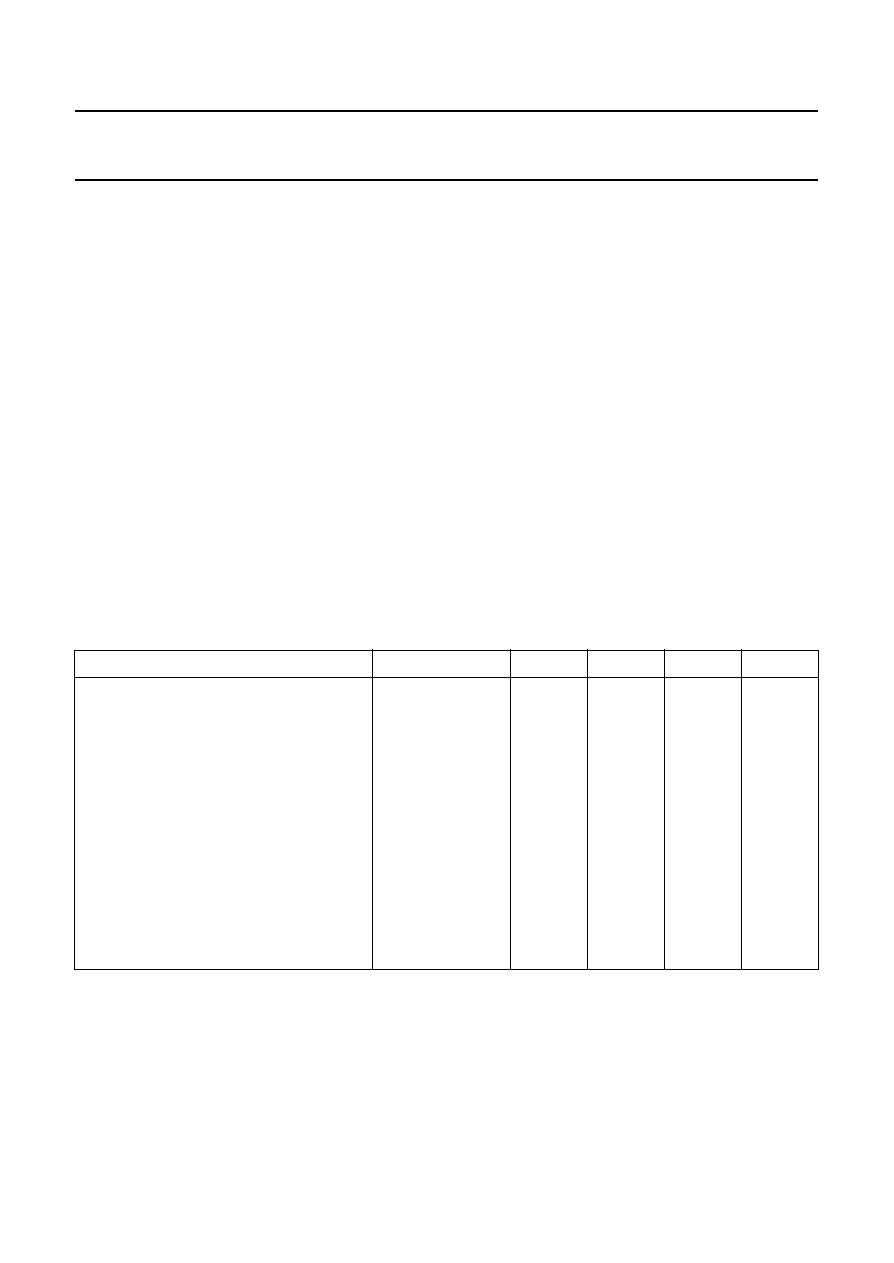
QUICK REFERENCE DATA
PACKAGE OUTLINE
13-lead SIL-bent-to-DIL; plastic power (SOT141R); SOT 141-6; 1996 July 23.
PARAMETER
CONDITIONS
SYMBOL
MIN.
TYP.
MAX.
UNIT
Supply voltage range
operating
V
P
6.0
14.4
18.0
V
non-operating
V
P
-
-
30
V
load dump protected
V
P
-
-
45
V
Repetitive peak output
current
I
ORM
-
-
4
A
Total quiescent current
I
tot
-
80
160
mA
Stand-by current
I
sb
-
0.1
100
µ
A
Switch-on current
I
sw
-
-
60
µ
A
Input impedance
|Z
I
|
50
60
75
k
Junction temperature
T
j
-
-
150
∞
C
Stereo application
Output power
R
L
= 4
; THD = 10% P
o
20
22
-
W
Supply voltage ripple
rejection
R
S
= 0
f = 100 Hz to 10 kHz
RR
48
-
-
dB
DC output offset voltage
|
V
O
|
-
-
150
mV
Channel separation
40
-
-
dB
Channel unbalance
|
G
v
|
-
-
1
dB
July 1994
4
Philips Semiconductors
Product specification
2 x 22 W BTL stereo car radio power
amplifier
TDA1552Q
PINNING
FUNCTIONAL DESCRIPTION
The TDA1552Q contains two identical amplifiers with differential input stages and can be used for bridge applications.
The gain of each amplifier is fixed at 26 dB. A special feature of this device is:
Mute/stand-by switch
∑
low stand-by current (< 100
µ
A)
∑
low mute/stand-by switching current (low cost supply switch)
∑
mute facility.
RATINGS
Limiting values in accordance with the Absolute Maximum System (IEC 134)
1
IP1
input 1
8
GND2
power ground 2 (substrate)
2
GND
ground (signal)
9
OUT2B
output 2B
3
V
P1
positive supply voltage 1
10
V
P2
positive supply voltage 2
4
OUT1A
output 1A
11
M/SS
mute/stand-by switch
5
GND1
power ground 1 (substrate)
12
n.c.
not connected
6
OUT1B
output 1B
13
IP2
input 2
7
OUT2A
output 2A
PARAMETER
CONDITIONS
SYMBOL
MIN.
MAX.
UNIT
Supply voltage
operating
V
P
-
18
V
non-operating
V
P
-
30
V
load dump protected
during 50 ms;
t
r
2.5 ms
V
P
-
45
V
Non-repetitive peak output current
I
OSM
-
6
A
Repetitive peak output current
I
ORM
-
4
A
Storage temperature range
T
stg
-
55
+
150
∞
C
Junction temperature
T
j
-
150
∞
C
AC and DC short-circuit-safe voltage
V
PSC
-
18
V
Energy handling capability at outputs
V
P
= 0 V
-
200
mJ
Reverse polarity
V
PR
-
6
V
Total power dissipation
see Fig.2
P
tot
-
60
W

