1.
General description
The TDA1566 is a car audio power amplifier with a complementary output stage realized
in BCDMOS technology. The TDA1566 has two Bridge Tied Load (BTL) output stages and
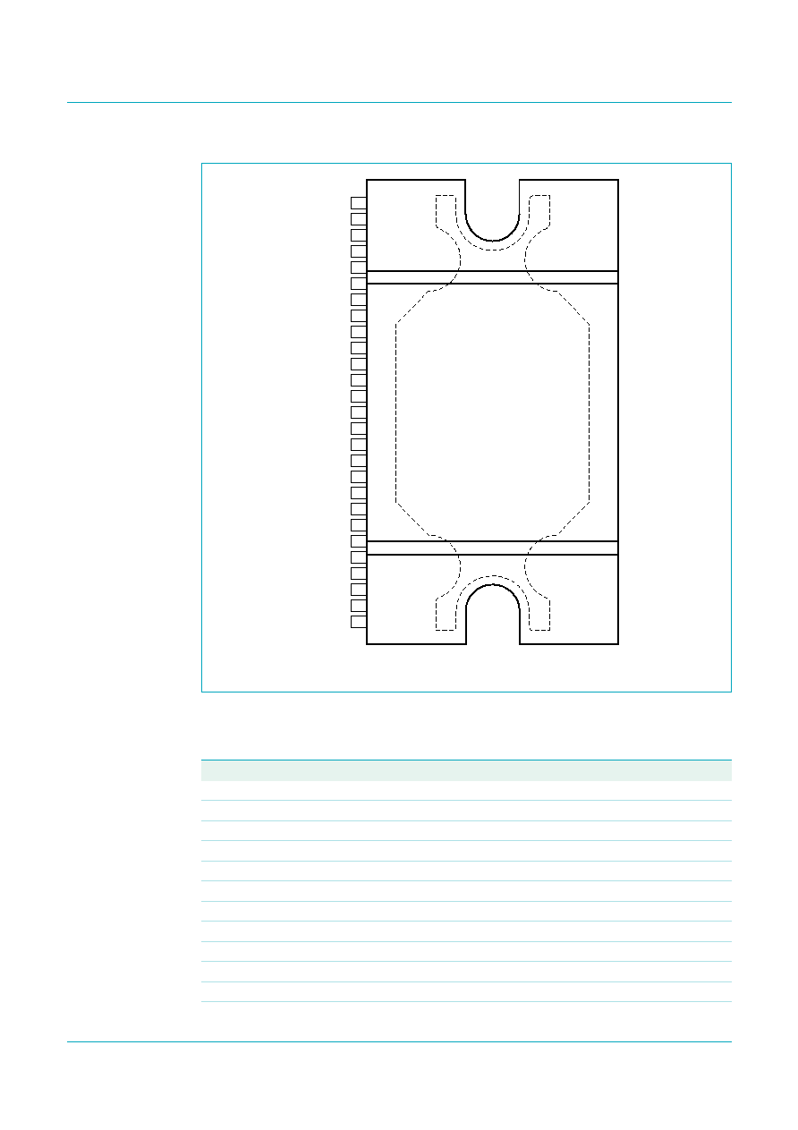
comes in a HSOP24 or DBS27P package.
The TDA1566 can be controlled with or without I
2
C-bus. With I
2
C-bus control gain settings
per channel and diagnostic trigger levels can be selected. Failure conditions as well as
load identification can be read with I
2
C-bus. The load identification detects whether the
outputs of a BTL channel are connected with a DC or AC load and discriminates between
a speaker load, a line driver load and an open (unconnected) load.
The TDA1566 can be configured in a single BTL mode and drive a 1
load. For the single
BTL mode it is necessary to connect on the Printed-Circuit Board (PCB) the outputs of
both BTL channels in parallel.
2.
Features
I
Operates in I
2
C-bus mode and non-I
2
C-bus mode
I
TH version: four I
2
C-bus addresses controlled by two pins; J version: two I
2
C-bus
addresses controlled by one pin
I
Two 4
or 2
capable BTL channels or one 1
capable BTL channel
I
Low offset
I
Pop free off/standby/mute/operating mode transitions
I
Speaker fault detection
I
Selectable gain (26 dB and 16 dB)
I
In I
2
C-bus mode:
N
DC load detection: open, short and speaker or line driver present
N
AC load (tweeter) detection
N
Programmable trigger levels for DC and AC load detection
N
Per channel programmable gain (26 dB and 16 dB, selectable per channel)
N
Selectable diagnostic levels for clip detection and thermal pre-warning
N
Selectable information on the DIAG pin for clip information of each channel
separately and independent enabling of thermal-, offset- or load fault
I
Independent short-circuit protection per channel
I
Loss of ground and open V
P
safe
I
All outputs short-circuit proof to V
P
, GND and across the load
I
All pins short-circuit proof to ground
I
Temperature controlled gain reduction at high junction temperatures
TDA1566
I
2
C-bus controlled dual channel 46 W/2
, single channel
92 W/1
amplifier with load diagnostic features
Rev. 01 -- 5 April 2006
Product data sheet
TDA1566_1
� Koninklijke Philips Electronics N.V. 2006. All rights reserved.
Product data sheet
Rev. 01 -- 5 April 2006
2 of 45
Philips Semiconductors
TDA1566
I
2
C-bus controlled dual channel/single channel amplifier
I
Fault condition diagnosis per channel: short to ground, short to supply, shorted lead
and speaker fault (wrongly connected)
I
Low battery voltage detection
I
TH version: pin compatible with the TDA8566TH1
3.
Ordering information
4.
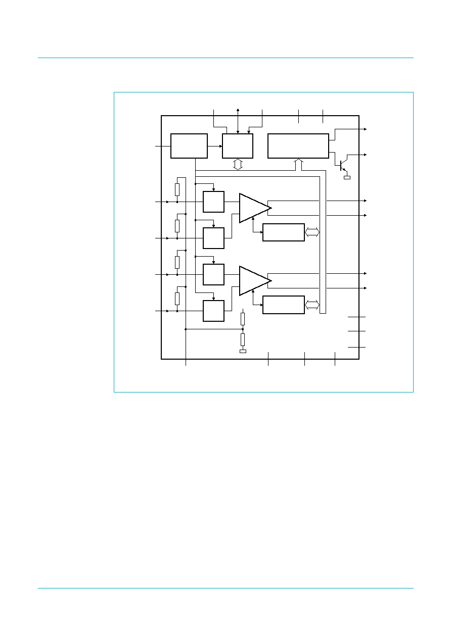
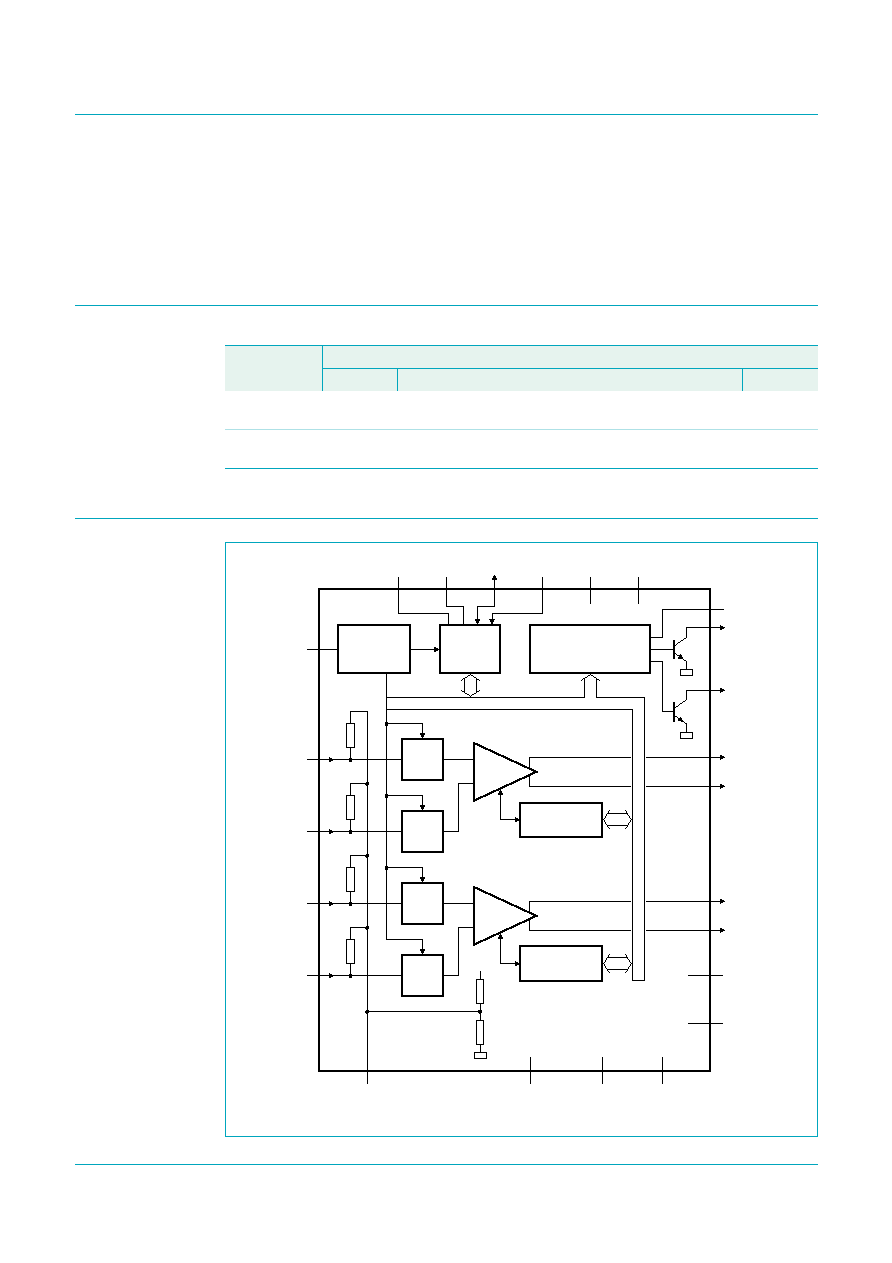
Block diagram
Table 1.
Ordering information
Type number
Package
Name
Description
Version
TDA1566TH
HSOP24
plastic heatsink small outline package; 24 leads; low
stand-off height
SOT566-3
TDA1566J
DBS27P
plastic DIL-bent-SIL (special bent) power package;
27 leads; lead length 6.8 mm
SOT827-1
Fig 1.
Block diagram (TDA1566TH)
001aac999
I
2
C-BUS
TDA1566TH
ADS1
SDA
SCL
V
P1
V
P2
ADS2
EN
9
6
5
14
23
8
7
IN1
+
IN1
-
10
11
IN2
+
2
IN2
-
3
26 dB/
16 dB
V
P
MODE
SELECT
SELECT DIAGNOSTIC
/CLIP DETECT
PROTECTION
/DIAGNOSTIC
4
SVR
SGND
PGND1
PGND2
12
17
20
24
TAB
15
1OHM
21
OUT2
-
OUT2
+
19
18
OUT1
-
OUT1
+
16
PROG
22
CLIP
13
DIAG
1
MUTE
MUTE
26 dB/
16 dB
PROTECTION
/DIAGNOSTIC
MUTE
MUTE
TDA1566_1
� Koninklijke Philips Electronics N.V. 2006. All rights reserved.
Product data sheet
Rev. 01 -- 5 April 2006
5 of 45
Philips Semiconductors
TDA1566
I
2
C-bus controlled dual channel/single channel amplifier
5.2 Pin description
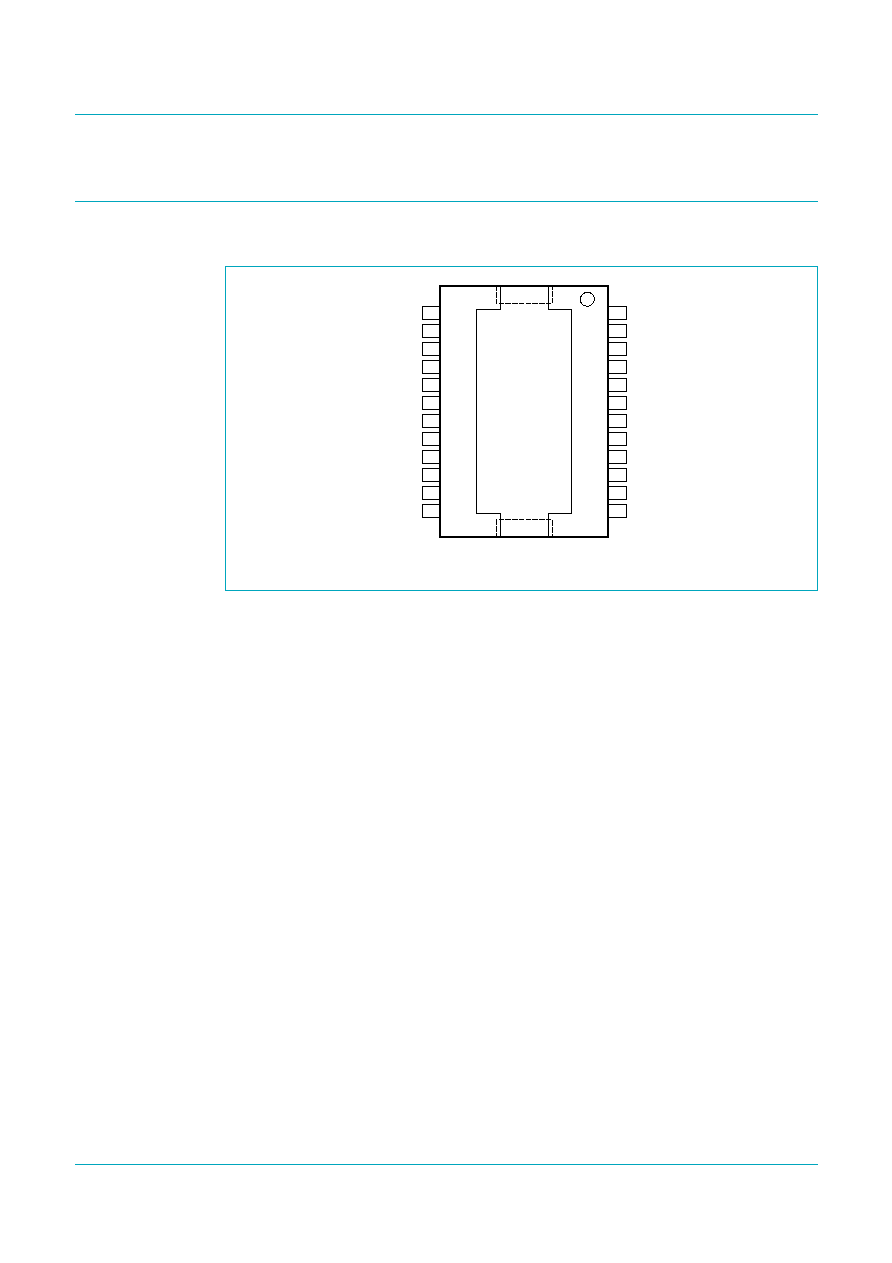
Fig 4.
Pin configuration for non mounting base TDA1566J (front)
TDA1566J
001aad007
EN
ADS1
IN1
+
IN1
-
SGND
DIAG
V
P1
1OHM
n.c.
OUT1
+
n.c.
PGND1
OUT1
-
n.c.
OUT2
+
PGND2
n.c.
OUT2
-
n.c.
PROG
V
P2
IN2
+
IN2
-
SVR
SCL
SDA
TAB
1
2
3
4
5
6
7
8
9
10
11
12
13
14
15
16
17
18
19
20
21
22
23
24
25
26
27
Table 2.
Pin description TDA1566TH
Symbol
Pin
Description
DIAG
1
diagnostic output
IN2+
2
positive input channel 2
IN2
-
3
negative input channel 2
SVR
4
supply voltage ripple decoupling
SCL
5
I
2
C-bus clock input
SDA
6
I
2
C-bus data input/output
EN
7
enable input
ADS2
8
I
2
C-bus address select bit 2
ADS1
9
I
2
C-bus address select bit 1
IN1+
10
positive input channel 1
IN1
-
11
negative input channel 1
SGND
12
signal ground