 | –≠–ª–µ–∫—Ç—Ä–æ–Ω–Ω—ã–π –∫–æ–º–ø–æ–Ω–µ–Ω—Ç: TDA2614 | –°–∫–∞—á–∞—Ç—å:  PDF PDF  ZIP ZIP |

DATA SHEET
Product specification
File under Integrated Circuits, IC01
July 1994
INTEGRATED CIRCUITS
TDA2614
6 W hi-fi audio power amplifier
July 1994
2
Philips Semiconductors
Product specification
6 W hi-fi audio power amplifier
TDA2614
FEATURES
∑
Requires very few external components
∑
No switch-on/switch-off clicks
∑
Input mute during switch-on and switch-off
∑
Low offset voltage between output and ground
∑
Hi-fi in accordance with IEC 268 and DIN 45500
∑
Short-circuit proof and thermal protected
∑
Mute possibility.
GENERAL DESCRIPTION
The TDA2614 is a power amplifier in a 9-lead single-in-line
(SIL9) plastic medium power package. It has been
especially designed for mains fed applications, such as TV
and radio.
QUICK REFERENCE DATA
ORDERING INFORMATION
Note
1. SOT110-1; 1996 August 21.
SYMBOL
PARAMETER
CONDITIONS
MIN.
TYP.
MAX.
UNIT
V
P
positive supply voltage range
15
-
42
V
P
O
output power
V
S
= 24 V; THD = 0.5%
-
6.5
-
W
G
v
internal voltage gain
-
30
-
dB
SVRR
supply voltage ripple rejection
-
45
-
dB
V
no
noise output voltage
-
70
-
µ
V
EXTENDED TYPE
NUMBER
PACKAGE
PINS
PIN POSITION
MATERIAL
CODE
TDA2614
9
SIL
plastic
SOT110
(1)

July 1994
3
Philips Semiconductors
Product specification
6 W hi-fi audio power amplifier
TDA2614
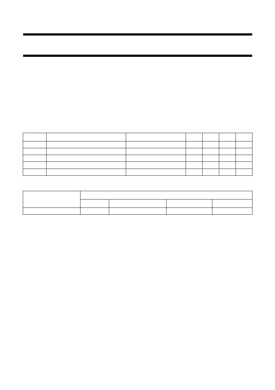
handbook, full pagewidth
MCD371 - 1
5
voltage
comparator
4 k
10 k
P
≠ V
THERMAL
PROTECTION
5 k
10 k
VA
B
V
P
+ V
ref1
V
ref3
V
ref2
+ V
ref2
≠ V
P
+ V
CM
20 k
VA
B
V
P
≠ V
680
20 k
ref1
V
6
P
GND / V
8
9
3
2
substrate
TDA2614
P
+ V
7
MUTE
1/2 V / GND
INV
INV
n.c.
n.c.
1
4
OUT
P
Fig.1 Block diagram.
July 1994
4
Philips Semiconductors
Product specification
6 W hi-fi audio power amplifier
TDA2614
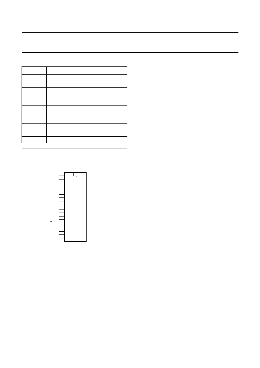
PINNING
SYMBOL
PIN
DESCRIPTION
n.c.
1
not connected
MUTE
2
mute input
1/2V
P
/GND
3
1/2 supply (or ground at
symmetrical power supplies)
n.c.
4
not connected
GND/
-
V
P
5
ground (or negative supply rail at
symmetrical power supplies)
OUT
6
output
V
P
7
supply voltage
INV
8
inverting input
-
INV
9
non-inverting input
Fig.2 Pin configuration.
handbook, halfpage
MCD367 - 1
1
2
3
4
5
6
7
8
9
P
V
OUT
MUTE
INV
TDA2614
/ GND
P
GND / ≠ V
n.c.
≠ INV
n.c.
P
1/2 V
FUNCTIONAL DESCRIPTION
The TDA2614 is a hi-fi power amplifier designed for mains
fed applications, such as radio and TV. The circuit is
optimally designed for asymmetrical power supplies, but is
also well-suited to symmetrical power supply systems.
An output power of 6 W (THD = 0.5%) can be delivered
into an 8
load with a supply of 24 V. The gain is internally
fixed at 30 dB, thus offering a low gain spread.
A special feature is the input mute circuit. This circuit
disconnects the non-inverting input when the supply
voltage drops below 10 V, while the amplifier still retains its
DC operating adjustment. The circuit features suppression
of unwanted signals at the input, during switch-on and
switch-off.
The mute circuit can also be activated via pin 2. When a
current at 300
µ
A is present at pin 2, the circuit is in the
mute condition.
The device is provided with two thermal protection circuits.
One circuit measures the average temperature of the
crystal and the other measure the momentary temperature
of the power transistors. These control circuits attack at
temperatures in excess of 150
∞
C, so a crystal operating
temperature of max. 150
∞
C can be used without extra
distortion.
With the derating value of 8 K/W, the heatsink can be
calculated as follows:
at R
L
= 8
and V
S
= 24 V, dissipation is 4.1 W.
With a maximum ambient temperature of 60
∞
C, the
thermal resistance of the heatsink is:
R
th
150
60
≠
4.1
----------------------
8
≠
14 K/W.
=
=
July 1994
5
Philips Semiconductors
Product specification
6 W hi-fi audio power amplifier
TDA2614
LIMITING VALUES
In accordance with the Absolute maximum System (IEC 134).
Note to the limiting values
1. For asymmetrical power supplies (with the load short-circuited), the maximum unloaded supply voltage is limited to
V
P
= 28 V, and with an internal supply resistance of R
S
4
, the maximum unloaded supply voltage is limited to
32 V (with the load short-circuited). For symmetrical power supplies, the circuit is short-circuit-proof up to
V
P
=
±
21 V.
SYMBOL
PARAMETER
CONDITIONS
MIN.
MAX.
UNIT
V
P
positive supply voltage
-
42
V
I
OSM
non-repetitive peak output current
-
4
A
P
tot
total power dissipation
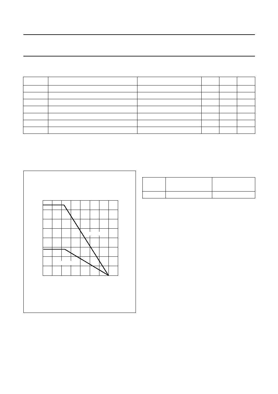
see Fig.3
-
15
W
T
stg
storage temperature range
-
55
+
150
∞
C
T
XTAL
crystal temperature
-
+
150
∞
C
T
amb
ambient operating temperature range
-
25
+
150
∞
C
t
sc
short circuit time
short circuit to ground; note 1
-
1
h
Fig.3 Power derating curve.
handbook, halfpage
≠ 25
0
50
150
16
12
4
0
8
MGA091 - 2
100
T ( C)
o
amb
P
(W)
tot
infinite heatsink
R = 14 K/W
th-hs
THERMAL RESISTANCE
SYMBOL
PARAMETER
THERMAL
RESISTANCE
R
th j-c
from junction to case
8 K/W